
Submitted:
12 May 2025
Posted:
12 May 2025
You are already at the latest version
Abstract
High-current electron beams can significantly enhance the productivity of variety of applications including medical radioisotope (RI) production and wastewater purification. High-power superconducting radio frequency (SRF) linacs are capable of producing such high-current electron beams due to the key advantage to operate in continuous wave (CW) mode. However, this requires an injector capable of generating electron bunches with high repetition rate and in CW mode, while minimizing beam losses to avoid damage to SRF cavities due to quenching. RF gating to the grid of a thermionic electron gun is a promising solution, as it ensures CW bunch generation at the repetition rate same as the fundamental or sub-harmonics of the accelerating RF frequency, with minimal beam loss. This paper presents the simulation results for the electron gun with RF gating generating high-current beam.
Keywords:
thermionic gridded electron gun
; RF gating
; SRF electron linac
; high average current
; CW
; short pulse electron generation
1. Introduction
High power, more specifically high-average-current electron linear accelerators (linacs) have the potential to revolutionize multiple fields, from medical radioisotope production [1,2] to environmental remediation [3,4]. In particular, for wastewater purification with electron linacs, there are many advantages, such as high productivity, reduced operating costs, and environmentally friendly operation with minimal waste [5,6]. To achieve higher average currents in e-linacs, it is more effective to use superconducting RF accelerating (SRF) cavities than normal-conducting ones. Since the heating caused by the RF power input in a normal-conducting RF cavites limit the ability to increase RF duty. On the other hand, if a high frequency superconducting RF cavity such as 1.3 GHz is used, cavity cooling with liquid helium is required which make the system impractical for most of the industrial applications including wastewater purification.
A promising solution is the integration of conduction cooled Nb3Sn based SRF [7,8,9] technology. It enhances the performance of e-linac by enabling continuous wave (CW) operation without requiring liquid helium for cooling. Neverthless, the full potential of SRF e-linacs, particularly for high-average-current operation, can only be realized if the injector system is capable of generating high-quality electron bunches with high repetition rate in CW mode. While significant progress has been made in high-peak-current injectors with pulse-mode operation, high-average-current injectors remain limited. As a result, despite significant advances in cavity material and shape, the lack of suitable injectors remains a major obstacle to fully exploiting the capabilities of SRF accelerators.
Our research aims to address this gap by developing a CW, high average current injector system optimized for SRF linacs. For stable operation of the SRF accelerator, the electron injector system should provide a properly shaped short bunches without tails and halo [10]. While RF photoinjectors [11] are commonly used to meet these requirements, they depend on complex drive lasers, which introduce additional costs, complexity, and maintenance challenges. In contrast, thermionic emission [12] offers a simpler, cost-effective alternative, providing high current density with benefits such as low maintenance and structural simplicity. However, the inherent challenge with thermionic emission i.e. the generation of continuous beam necessitates precise bunching mechanisms to achieve compatibility with SRF linac operation.
This issue can be solved using a cathode grid of electron gun which controls the temporal structure of the electrons emitted from cathode to produce a bunched beam. Additionally, a carefully designed bunching system is essential to compress the bunches into a suitable time profile for smooth injection and acceleration in the SRF cavities. To meet these requirements, we have designed an injector using KUCODE [13] that combines a thermionic gridded electron gun with a conduction cooled 1.3 GHz 3-cell buncher [14]. Our initial target is to generate a 10 mA beam, requiring approximately 8 pC per bunch at a 1.3 GHz repetition rate, with plans to achieve higher currents in future improvements. By this design, we introduce a novel buncher, which can compress the electron bunches of full width (FW) ≤ 400 ps to the suitable longitudinal bunch profile ensuring the seamless injection to the main accelerator linac. This indicates that generating electron bunches of FW ≤ 400 ps with the repetition rate of 1.3 GHz and in a CW mode from the electron gun is crucial for this design.
While alternative electron gating approaches exist, using available grid pulsers such as FETs [15] and avalanche pulsers [16]. They have significant limitations. FET pulsers produce MHz repetition rate but are limited to produce ~170 ps RMS (FW >> 400 ps) bunches, while avalanche pulsers can achieve short bunches of ~ 60 ps RMS (FW ~ 400 ps) but only at kHz rates. We found an effective solution to this challenge which is applying RF gating to the grid of the thermionic electron gun. Previous studies on RF gating for thermionic guns have demonstrated the feasibility of generating electron bunches with the required parameters [17,18,19]. Additionally, RF gating approach not only gates the electrons effectively to produce a short bunched beam but also allows the generation at the desired repetition rate of 1.3 GHz with minimal beam loss.
This paper presents the theoretical basis, simulation outcomes validating the RF gating method. By resolving the limitations of high-average-current injectors and leveraging the benefits of thermionic emission, this work marks a significant step forward in advancing SRF electron linac technology for high-power applications.
2. Thermionic Gridded Electron Gun
Electron gun [20] was developed based on the existing thermionic gridded gun at our facility, using a commercially available cathode (Y646B, diameter 8 mm) from CPI Inc. [21]. Grid in front of the cathode has a gap of 0.16 mm with the grid wire specifications as shown in Figure 1 (a). The Wehnelt electrode has an angle of 60°. The anode, featuring a bore diameter of 9 mm, is positioned 28.5 mm from wehnelt as shown in Figure 1 (b). The system is currently in use at the test bench of our facility. In this paper, simulations performed for RF gating, consider the same geometry and the arrangement of the cathode and anode of the electron gun system.
3. Theoretical Model and Simulation Setup for RF Gating
3.1. RF Gating Mechanism
In RF gating mechanism [17,18,19], the emitted electron beam is modulated by combination of RF and DC bias voltages for short bunch generation. This is achieved by using electron gun assembly where DC high voltage (HV) is applied between anode and cathode with HV power supply, RF waves generated from RF source are fed in between cathode and grid space using coaxial structure. Additionally, a small negative DC bias voltage is applied across the cathode and grid using a bias power supply, as illustrated (roughly) in Figure 2(a). The resultant potential difference between the cathode and grid is described by Eq. 1 and shown in Figure 2(b):
Where is the total grid voltage, is the small DC biasing voltage, and is the amplitude and the frequency of the RF waves respectively, and () is the half bunch-length. is the offset emission voltage caused by leakage of the HV electric field through the grid. Due to the leakage field, electron emission occurs for a slightly longer duration than the intended emission area, as shown by the red line in Figure 2(b). The bunch repetition rate in this mechanism is determined by the RF wave frequency which in our case is 1.3 GHz.
Since a thermal energy of the electrons is usually of the order of millivolts (mV) and the negative applied to the grid is of the order of volts (V), electrons from the cathode are allowed to emit and move towards grid only when . The condition satisfies for and leads to the Eq. 2 at the extremes.
Assuming a linear relationship between the emitted current and the applied grid voltage, as supported by prior work [17,18,19], the emitted current can be expressed as:
Where represents the transconductance of the gun i.e. the emission capability of the gun. By integrating the current over the emission area, the total bunch-charge can be calculated as given by Eq. 4.
This equation demonstrates that depends on , , and . By adjusting the and , the emission area () can be controlled and thereby tuning both the bunch-length () and bunch-charge ().
The longitudinal properties of the electron bunch in the RF gating mechanism are thus entirely governed by the applied grid voltages. As a result, operating the gun in the space-charge-limited regime is preferred, as it allows for complete manipulation of the beam by adjustuting the grid voltages, enabling precise control over the electron emission.
3.2. Simulation setup for RF gating in KUCODE
The principle of the RF gating described in the previous section does not account for factors such as space charge effects, effect due to the emission of electrons from different transverse distance from the axis, and beam dynamics between the grid and anode. To address these aspects, we analysed the performance of the electron gun with RF gating using KUCODE with the simulation setup as shown in Figure 3.
KUCODE being a 2.5-dimensional particle tracking code posed limitations in modelling the grid as a mesh structure. Therefore, we approximated the grid as an imaginary, perfectly conducting plate with a thickness of 20 µm (same as actual grid wire thickness shown in Figure 1(a)), positioned 160 µm from the cathode surface (). While this plate is physically invisible to the electrons, it allows for the application of DC bias voltage in the simulation. With this approximation, two issues arose. First, no field rigion within the grid metal plate of 20 µm, causing an unnecessary pulse lengthening whereas in practice, there is no such region. To address this issue, a thin grid metal plate of 1 nm is considered. Second, as KUCODE does not model the grid as a mesh structure, which limits its ability to account for leakage fields i.e. cutoff effect due to the high voltage (HV), thus the effect is ignored ().
To drive the grid with the RF voltage, we modeled a capacitvely loaded coaxial cavity resonating at an eigenfrequency of 1.3 GHz. The parameters of this cavity are as shown in Figure 4 and given in Table 1.
Electron emission from the cathode surface in the simulations is uniform in both radial and longitudinal directions, with an initial monoenergetic energy of 0 eV and current density of 0.2 A/cm². This current density corresponding to a total DC emission current of 100 mA which can be easily achieved using Y-646B cathode with a nominal heater voltage in our experimental setup. Thus, simulation parameter considered for this study is consistent with our experimental setup.
To be compatible with the designed 3-cell buncher in Ref. [14], the generated electron bunch must achieve β = 0.5. Given this requirement, the accelerating voltage between the cathode and the anode in this study is set at 80 kV. To apply RF voltage, we estimated the maximum achievable based on the available RF amplifier in our facility. The amplifier delivers a maximum power () of 96 W and with an impedance () of approximately 45 Ω (measured using a network analyzer) between the cathode and the grid in our gun, the maximum is calculated to be of approximately 65 V using the relation: . Consequently, in the KUCODE simulations, was fixed at 65 V, while was varied from 0 to -65 V to evaluate the gun’s performance under different operating conditions. The primary objective of the simulations was to estimate as the function of and , and to confirrm that the bunch of and with 1.3 GHz pulse repetition (), can be produce. Results of this study has been discussed in detail in the following section.
5. Results and Discussion
5.1. Performance of the RF Gated Gun (Cathode – Grid Space)
The bunch characteristics, specifically the full width () and charge (), are analyzed at two positions: near cathode (z = 5 µm) and at the grid (z = 160 µm). is calculated with the threshold of 0.01% of the peak value of . The dependence of these parameters on the absolute value of biasing voltage i.e. with a fixed (65 V) is presented in Figure 5.
Results indicate that for the same , both and are smaller at grid (z = 160 µm) compared to near cathode (z = 5 µm). To discuss this calculation outcome, we analyse the longitudinal phase space distribution as shown by Figure 6. In RF gating, electrons are emitted within (Figure 2 (b)), which corresponds to the emission at different phase of the RF field, as illustrated in Figure 6(a). Due to the phase difference, electrons emitted within i.e. the front part of the bunch, gain energy more than those emitted within i.e. the tail part of the bunch while moving from cathode to grid. Consequently, at the grid, energy of the front part of the bunch is higher than that of the tail part, as shown in Figure 6(b). In this process, the electrons emitted from cathode at time close to do not gain sufficient energy to cross the cathode-grid gap. As a result, these electrons fail to reach the grid, contributing to the reduction in both and , which explains why are smaller at the grid than near the cathode.
.
Figure 5 further shows that both and continue to decrease with increasing , eventually dropping to zero for . This trend is a fundamental characteristic of the RF gating mechanism. Since the emission area represented by reduces with increasing explaining the reason for reduction in both parameters. However, to further understand why drops to zero for , we examined the electron transit time and the electron acceleration time. Where, the electron acceleration time corresponds to the time in which electrons emit from cathode and accelerate towards grid. The electron acceleration time is therefore same as the emission time . The transit time on the other hand represents an average time required for an electron to cross the cathode-grid gap () under the effect of time varying . is determined through the Eq. (5), (6), (7) and (8) given below. The equations consider the integrated RF field as given in Eq. (7), experience by the emitted electrons over the duration of the emission area and calculates as follows:
Where : rest mass of electron, : Lorentz factor, and : velocity of electron. The results of transit time and acceleration time calculations are presented in Figure 7. For , exceeds the acceleration time , indicating insufficient energy imparted to emitted electron to cross the cathode-grid gap within the available acceleration time. Consequently, electrons fail to reach the grid and return to the cathode, causing and to drop to zero. The longitudinal phase space distribution for in Figure 6 confirms this behavior. Figure 6(a) shows electron emission, while Figure 6(b) demonstrates no electrons reaching the grid.
.
Lastly, Figure 5(a) and (b) showing and at grid, helps to determine the optimal for achieving the required (~ 8 pC) and smallest achievable . This is because, electrons reaching the grid do not loss further downstream. Furthermore, the discussion on transit time and acceleration time suggests that the smallest achievable occurs at , since beyond this , electrons could not reach the grid to form bunch. However, the corresponding is only ~5 pC as seen in Figure 5(b). This can be resolved by increasing the emission current density from cathode. with higher emission current density is as shown in Figure 8. It indicates that with , ≥ 8 pC can be achieved, if the current density is increased from 0.2 (earlier setting) to 0.4 A/cm². This higher current density can also be achieved easily by slightly increasing the heater voltage. Thus, both conditions of minimum and required is satisfied. As expected, there is no significant difference in obtained with these two current densities at the grid, illustrated by Figure 8.
Therefore, a detailed analysis of the bunch evolution, including its behavior within the cathode-grid gap and further downstream to the buncher position, is performed for and current density of 0.4 A/cm2 in the following sections. For this analysis, longitudinal phase space distribution is presented as Δ vs time where with : kinematic energy of individual electron and mean kinematic energy of the bunch.
While analyzing the evolution of longitudinal phase space distribution of the bunch from cathode to grid for (Figure 9), we observed that the density of the bunch head is higher than the tail. Careful analysis suggests that this comes from the interplay between time-dependent electron emission and . At (Figure 2 (b)), electron emission begins and gradually experience the high accelerating field. Subsequently, the electrons accelerated by the high accelerating field can catch up with the emitted electrons before them. This causes longitudinal compression of the electrons emitted in this region, giving higher density at the bunch head. Electrons emitted in the later region can no longer catch up the earlier emitted electrons. This leads to a more uniform density distribution in the remaining part of the bunch until falls below the emission threshold and the density drops to zero, as depicted by Figure 9 (a). This asymmetric electron distribution from the initial emission time plays a crucial role in shaping the bunch evolution downstream of the grid. As shown in Figure 9 (b), the distribution remains unchanged at the grid i.e. high current density at bunch head. The further evolution downstream the grid is discussed in the following sections.
5.2. Performance of the RF Gated Gun (Grid – Anode Space)
and obtained for different at z = 40 mm i.e. 2 mm downstream the anode is as shown in Figure 10 (a) and (b) respectively. As expected, downstream the anode (z= 40 mm) remains same as at grid (z= 160 µm) indicating no loss of between the grid and the anode. However, increases as bunch moves from grid to anode for the same .
To understand the increase of and the evolution of bunch downstream the grid up to the anode, the longitudinal phase space distribution is analysed for as shown in Figure 11. The result reveals an energy spread within the bunch. To investigate the origine of this spread, simulations were conducted both with and without the space charge effect. The results of the simulation without space charge effects are shown in Figure 12. The comparison of Figure 11(c) and Figure 12(c) clearly demonstrates that the high energy of the bunch head is primarily due to the space charge effect. Space charge effect is more pronounced at the bunch head than at bunch tail. The reason is an asymmetric temporal distribution of the bunch i.e. high density at bunch head whose origin is described in previous section. As a result, a stronger accelerating force due to space charge on the bunch head compared to the decelerating force on the bunch tail is present. This explains both the high energy of the bunch head and the longitudinal expansion of the bunch giving longer at z = 40 mm than at z = 160 µm. However, the energy spread observed after the grid i.e. at z= 0.5 mm, as visible in Figure 11 (a) and Figure 12 (a), is not attributable to the space charge effect. A detailed analysis revealed that this spread arises from the difference in the HV field experienced by electrons at different transverse positions. Figure 13 illustrates the HV field along the axis i.e. at r = 0 and at r = 4mm. As a result, electrons along the axis gain higher energy compared to those at the outer positions, resulting in an energy spread within the bunch at this position of z= 0.5 mm.
5.3. Performance of the RF Gated Gun (Anode – Buncher Space)
obtained for different at the buncher position (z = 500 mm) is shown in Figure 14 (a). The optimal case of produces the smallest of approximately 148 ps and Q = 8.96 pC. The corresponding longitudinal phase space distribution for this optimal configuration is presented in Figure 14 (b). The transverse slice emittance of the electron bunch is illustrated in Figure 15. While the calculated emittance remains below 20 mm-mrad—a value typically considered favourable for SRF injection—this parameter is not the primary concern for our aimed application of wastewater purification.
This overall analysis demonstrates that the design requirement of a ≤ 400 ps can be achieved using RF gating. Since the calculations do not account for cutoff effects, a safety margin is necessary. Nevertheless, the smallest achievable with the required Q obtained at is significantly shorter than the 400 ps requirement. We anticipate this will remain within acceptable limits even when accounting for cutoff effects. Additionally, the energy spread for the bunch at buncher position is approximately 6 %; however, our 3-cell buncher design is not sensitive to energy spread. To verify this, we propagated this bunch through our 3-cell buncher using KUCODE and the result is as shown in Figure 16. obtained after 3-cell is suitable to pass through the main accelerator cavity with = 10 ps and mean kinematic energy 1.2 MeV.
5.5. Other ways to Reduce the Bunch-Length Further
For smallest , previous section finalizes with which gives , where , shown in Figure 2(b). However, can also be achieved with other combinitions of and . We therefore investigated the effect of other combinitions as shown in Figure 17. While the current RF amplifier at our facility restricts us to , future improvements may allow for higher values. In this study, we therfore considered the combinition of with higher also.
Our analysis reveals that combinations with higher values produce shorter bunch-lengths. This relation can be understood from Figure 18, which demonstrates how the emission area for different and combinations (all yielding ) become sharper with increasing and , resulting in shorter . However, Figure 17 also demonstrates that increasing voltages lead to significant reduction in . This creates a critical trade-off between achieving shorter and maintaining sufficient . The simulations performed in this section indicate that with would yield the required and < 148 ps but require and RF power more than 100W.
The test bench to validate the simulation study is currently under developement at our facility. Simulations suggest that our current setup with available 1.3 GHz RF amplifier (100W giving ) satisfies the requirements adequately ( 400 ps). Therefore, the immediate investment in higher-capacity RF amplifiers is not considered for our test bench.
6. Conclusions
This study presents a comprehensive analysis of an RF-gated electron gun system, demonstrating its capability to produce electron bunches with characteristics suitable for our experimental requirements. Through detailed simulations using KUCODE, we established that the optimal operating parameters of with yield a bunch-length of approximately 148 ps with bunch-charge of 8.96 pC, comfortably meeting our design requirement of ≤ 400 ps and ≥ 8 pC. The analysis reveals fundamental physical mechanisms governing bunch formation, including space charge effects and field interactions. While further performance improvements are theoretically possible with higher values, the current configuration provides an effective balance between performance and practical implementation constraints. These findings establish a solid foundation for the operational deployment of the RF-gated electron gun in our experimental setup.
Author Contributions
A.K., T.M. and S.K. conceived the physics concept and simulations; K.M contributed to code development and numerical validation. I.N., K.-i.N., K.S., and K.T. proposed the test bench framework; F.H., H.Y., P.K., K.K, and H.A. performed proofreading & editing; H.H. supervised the overall study; A.K. and S.K. wrote the paper. All authors have read and agreed to the published version of the manuscript.
Funding
This work is partially supported by JSPS KAKENHI Grant Numbers 23H00101, Grant-in-Aid for Scientific Research(A).
Data Availability Statement
Not applicable.
Conflicts of Interest
The authors declare no conflict of interest.
References
- Diamond, W. T., and C. K. Ross. "Actinium-225 production with an electron accelerator." Journal of Applied Physics 129.10 (2021). [CrossRef]
- Starovoitova, Valeriia N., Lali Tchelidze, and Douglas P. Wells. "Production of medical radioisotopes with linear accelerators." Applied Radiation and Isotopes 85 (2014): 39-44. [CrossRef]
- Chmielewski, Andrzej G., and Bumsoo Han. "Electron beam technology for environmental pollution control." Applications of radiation chemistry in the fields of industry, biotechnology and environment (2016): 37-66. [CrossRef]
- Borrely, S. I., et al. "Radiation processing of sewage and sludge. A review." Progress in Nuclear Energy 33.1-2 (1998): 3-21. [CrossRef]
- Londhe, Kaushik, et al. "Energy evaluation of electron beam treatment of perfluoroalkyl substances in water: a critical review." ACS ES&T Engineering 1.5 (2021): 827-841. [CrossRef]
- Trojanowicz, Marek, et al. "Gamma-ray, X-ray and electron beam based processes." Advanced oxidation processes for waste water treatment. Academic Press, 2018. 257-331. [CrossRef]
- H. Hama, S. Miura, “Toward Superconducting Electron Accelerators for Various Applications.”, physica status solidi (a) 218, 2000294 (2021). [CrossRef]
- Y. S. Pavlov, V. V. Petrenko, P. A. Alekseev, P. A. Bystrov, O. V. Souvorova, “Trends and opportunities for the development of electron-beam energy-intensive technologies”, Radiation Physics and Chemistry 198, 110199 (2022). [CrossRef]
- G. Ciovati, J. Anderson, B. Coriton, J. Guo, F. Hannon, L. Holland, M. LeSher, F. Marhauser, J. Rathke, R. Rimmer, T. Schultheiss, and V. Vylet, “Design of a cw, low-energy, high-power superconducting linac for environmental applications.”, Phy. Rev. Acc. and Beams 21, 091601 (2018). [CrossRef]
- I Gonin, S Kazakov, R Kephart, T Khabiboulline, T Nicol, N Solyak, J Thangaraj, V Yakovlev, “Built-in thermionic electron source for an SRF linacs”, IPAC2021 (Brazil, 2021) THPAB156. [CrossRef]
- Asaka, Takao, et al. "Low-emittance radio-frequency electron gun using a gridded thermionic cathode." Physical Review Accelerators and Beams 23.6 (2020): 063401. [CrossRef]
- Sprangle, Phillip, et al. "High average current electron guns for high-power free electron lasers." Physical Review Special Topics—Accelerators and Beams 14.2 (2011): 020702. [CrossRef]
- K Masuda, Development of Numerical Simulation Codes and Application to Klystron Efficiency Enhancement, Ph. D Thesis, Dept. of Engineering, Kyoto Univ. (1998).
- Kavar, A. B., et al. "NUMERICAL STUDY OF 5 MeV SRF ELECTRON LINAC FOR WASTEWATER PURIFICATION." 32nd Linear Accelerator Conference, LINAC 2024. JACoW Publishing, 2024.
- N. Nishimori, R. Nagai, R. Hajima, T. Shizuma, E.J. Minehara, EPAC2000 (Vienna, 2000), MOP5A06.
- S. G. Sheng, G. Q. Lin, Q. Gu, D. M. Li, Proceedings of the second Aasia Particle Accelerator Conference (APAC’01) (China, 2001), TUBU04.
- R. J. Bakker, C. A. J. van der Geer, A. F. G. van der Meer, P. W. van Amersfoort, W. A. Gillespie, G. Saxon, Nucl. Instr. Meth. Phys. Research A 307, 543 (1991). [CrossRef]
- Gold, S. H., et al. "Development of a high average current rf linac thermionic injector." Physical Review Special Topics—Accelerators and Beams 16.8 (2013): 083401. [CrossRef]
- Zhang, Liang, et al. "Electron injector based on thermionic RF-modulated electron Gun for particle accelerator applications." IEEE Transactions on Electron Devices 67.1 (2019): 347-353. [CrossRef]
- Kavar, Anjali B., et al. "Numerical Study of a High Current Thermionic Electron Gun for a Superconducting Radio Frequency Linac." e-J. Surf. Sci. Nanotechnol.22,212–219 (2024). [CrossRef]
- https://www.cpii.com/product.cfm/9/22/131.
Figure 1.
(a) Assembly of EIMAC Y646B thermionic gridded cathode (b) Electron gun geometry.
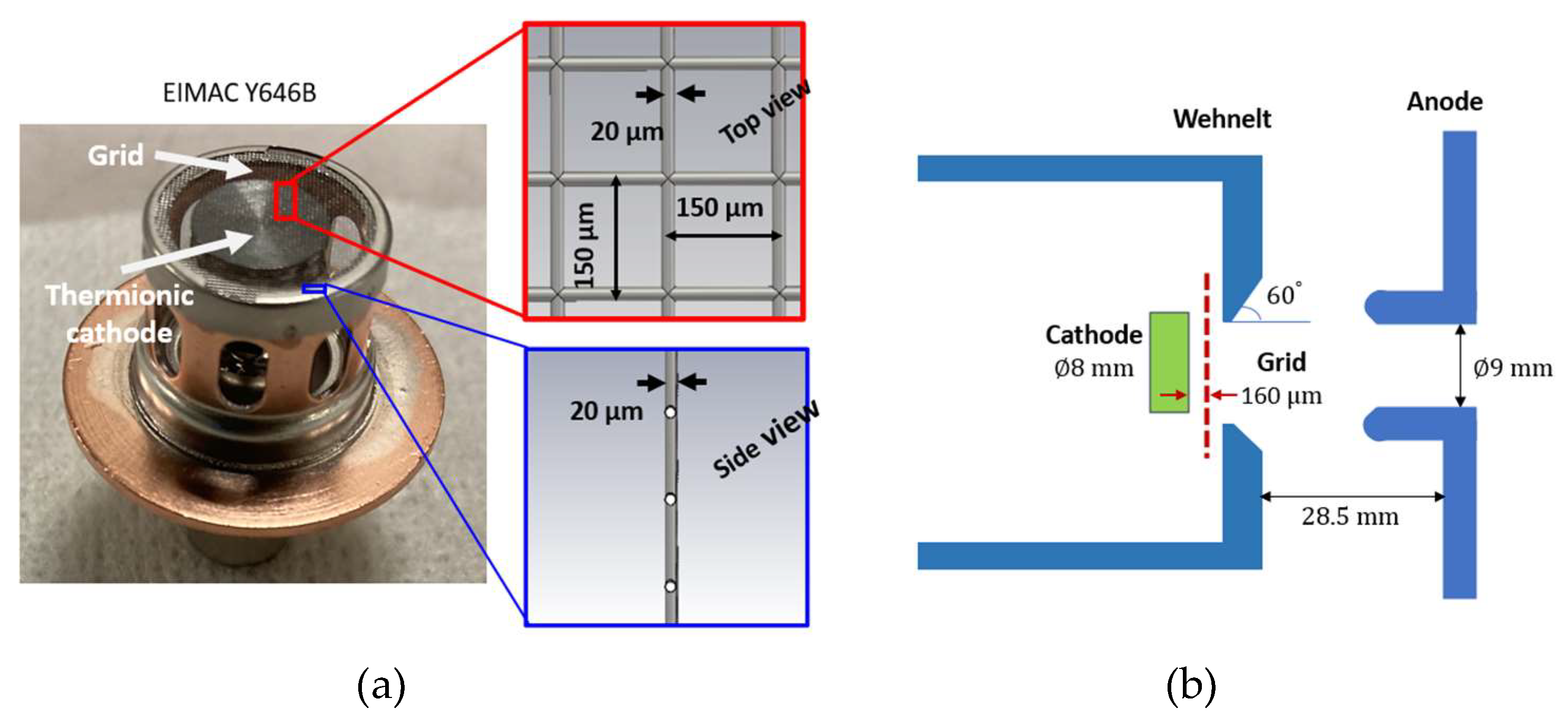
Figure 2.
(a) RF and DC voltages applied between the electrodes of electron gun. (b) Resultant potential difference between cathode and grid with the emission area shown by red shading.
Figure 2.
(a) RF and DC voltages applied between the electrodes of electron gun. (b) Resultant potential difference between cathode and grid with the emission area shown by red shading.
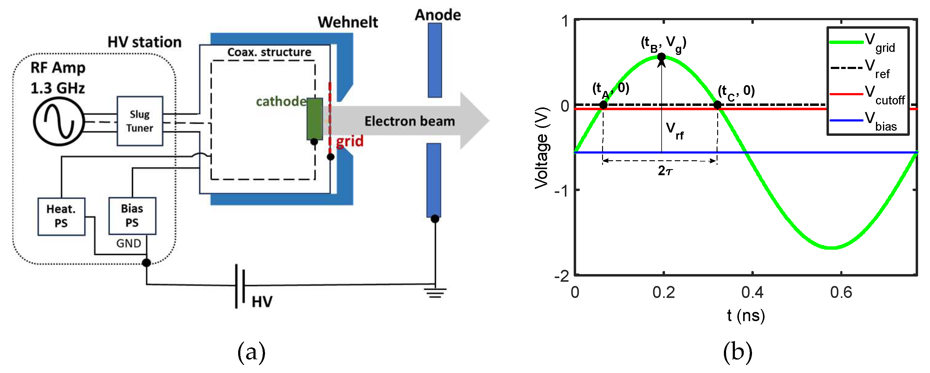
Figure 3.
Simulation set for RF gating study in KUCODE.
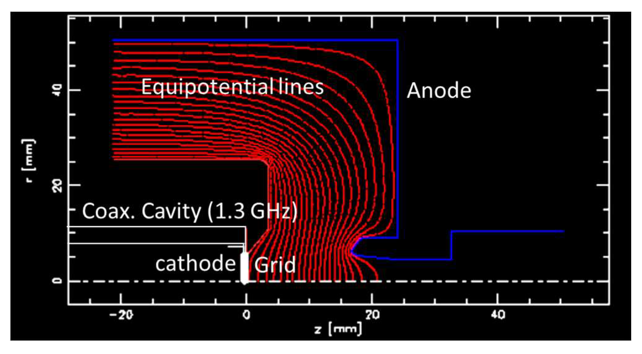
Figure 4.
1.3 GHz coaxial cavity and dimensions.
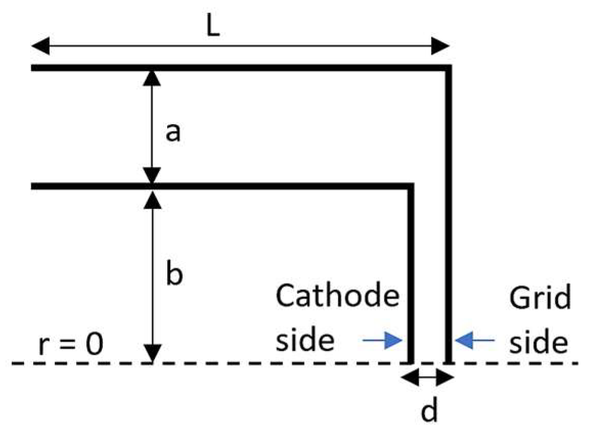
Figure 5.
(a) bunch-length and (b) bunch-charge near cathode (z = 5 µm) and at the grid (z = 160 µm).
Figure 5.
(a) bunch-length and (b) bunch-charge near cathode (z = 5 µm) and at the grid (z = 160 µm).
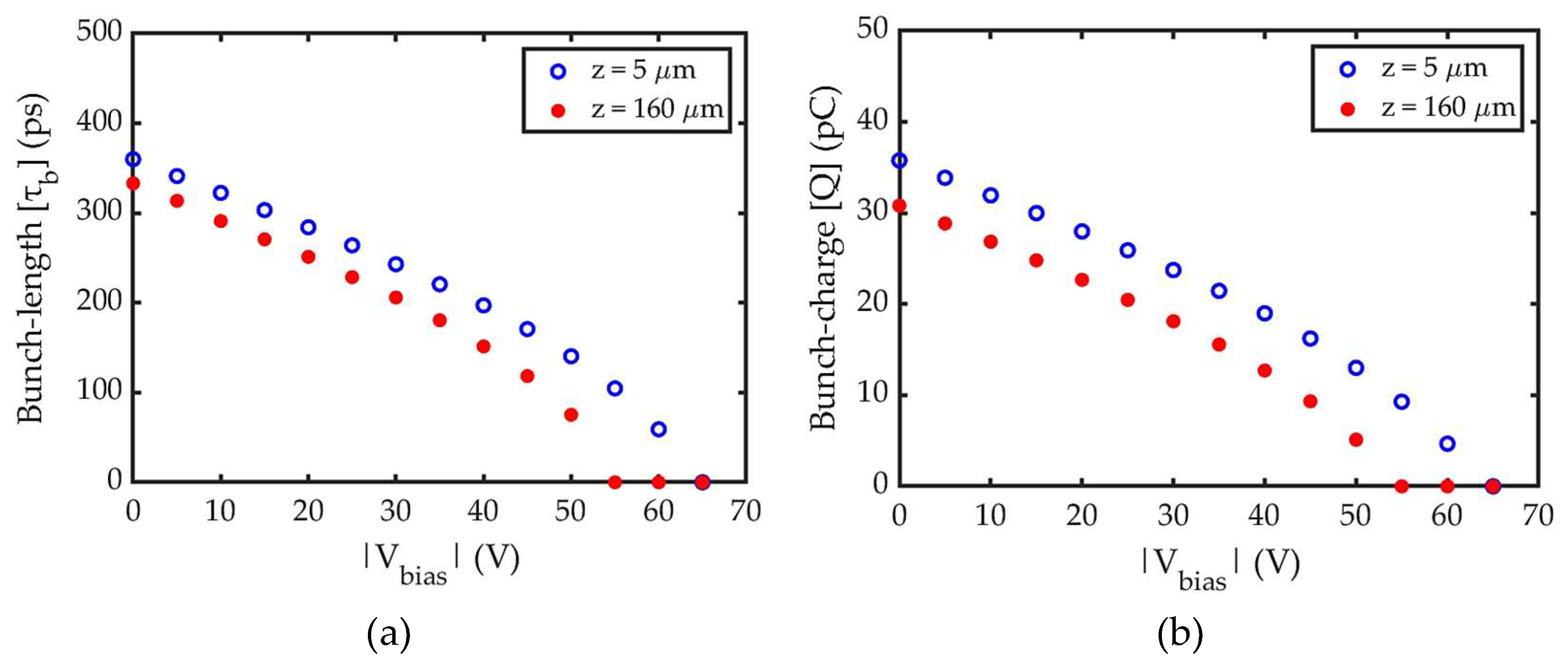
Figure 6.
longitudinal phase space distribution (kinematic energy of the bunch vs time) (a) near cathode (z = 5 µm) and (b) at the grid (z = 160 µm) for different .
Figure 6.
longitudinal phase space distribution (kinematic energy of the bunch vs time) (a) near cathode (z = 5 µm) and (b) at the grid (z = 160 µm) for different .
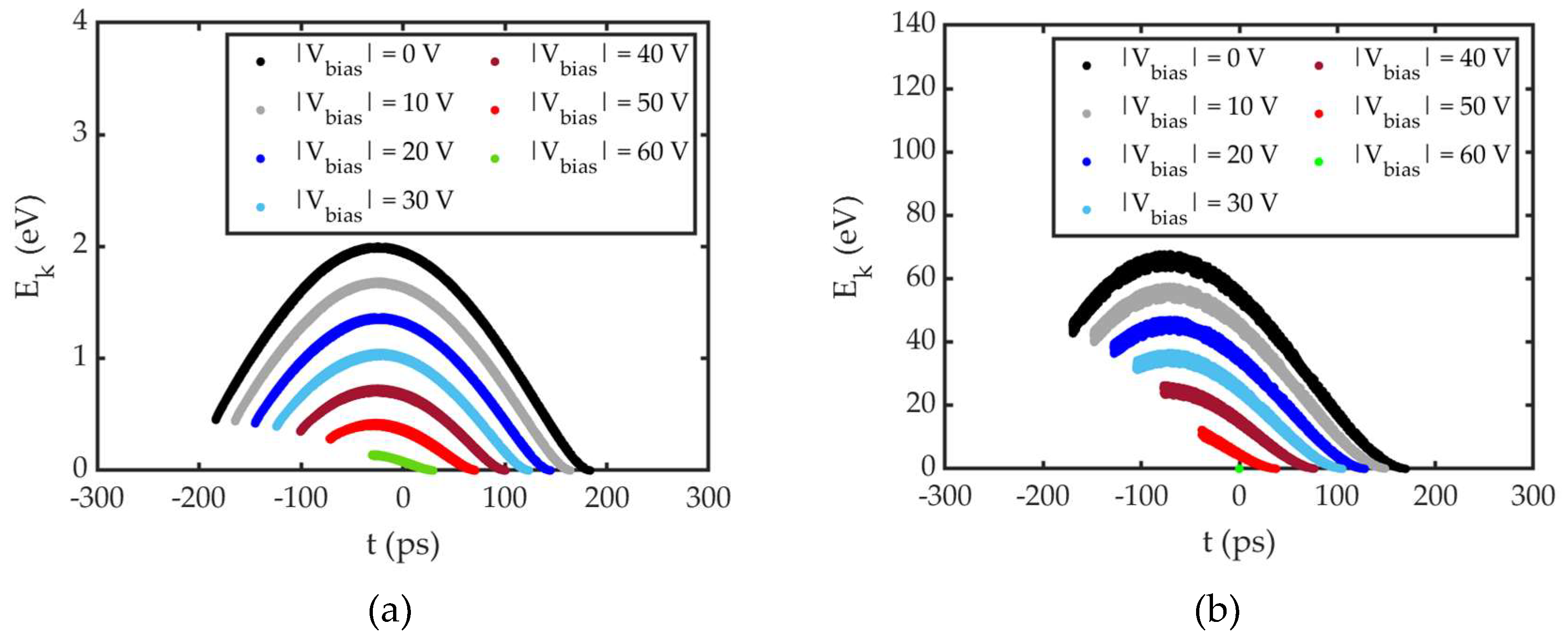
Figure 7.
Electron acceleration time and the transit time for different .
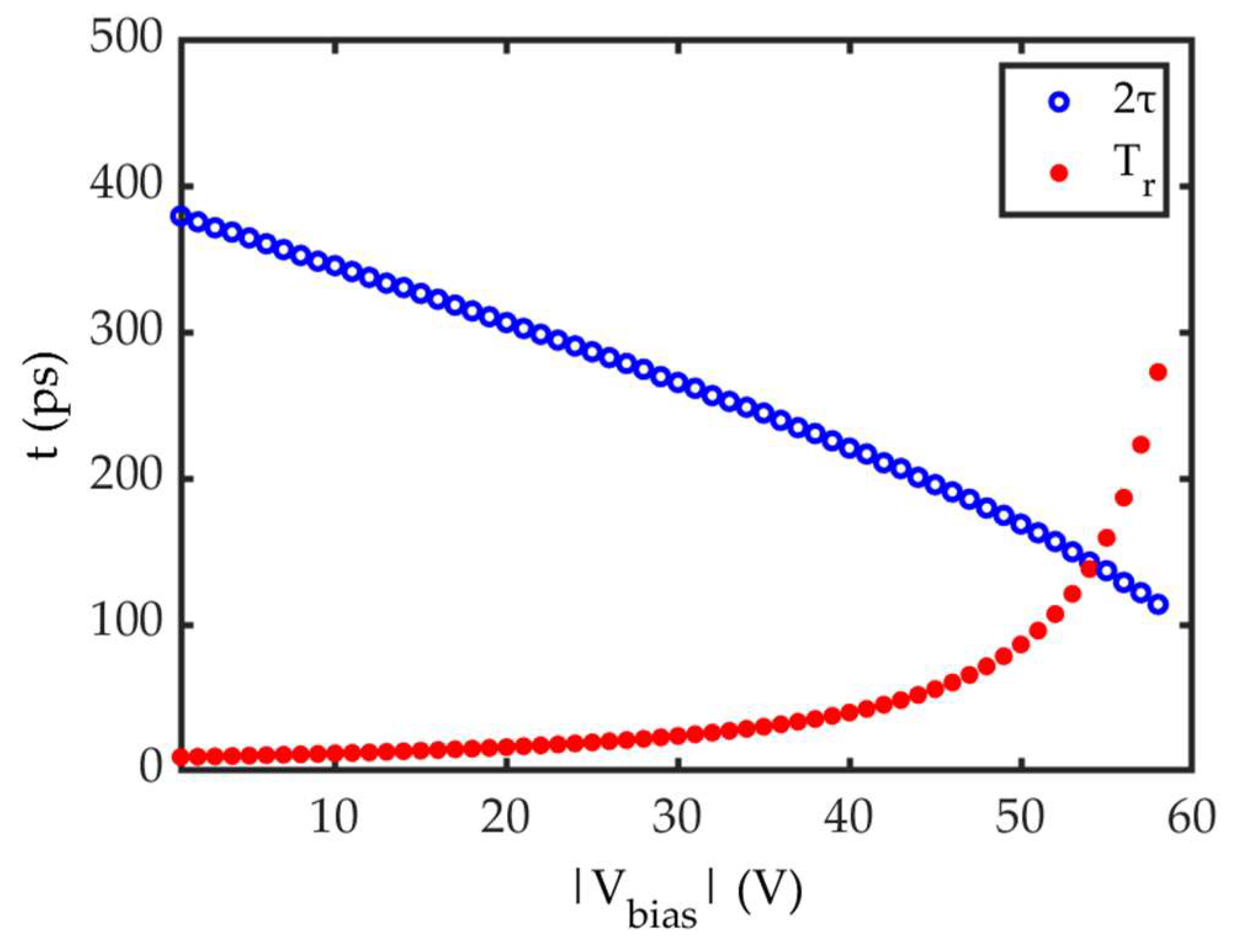
Figure 8.
Bunch-charge and Bunch-length as a function of different emission current density of the cathode at .
Figure 8.
Bunch-charge and Bunch-length as a function of different emission current density of the cathode at .
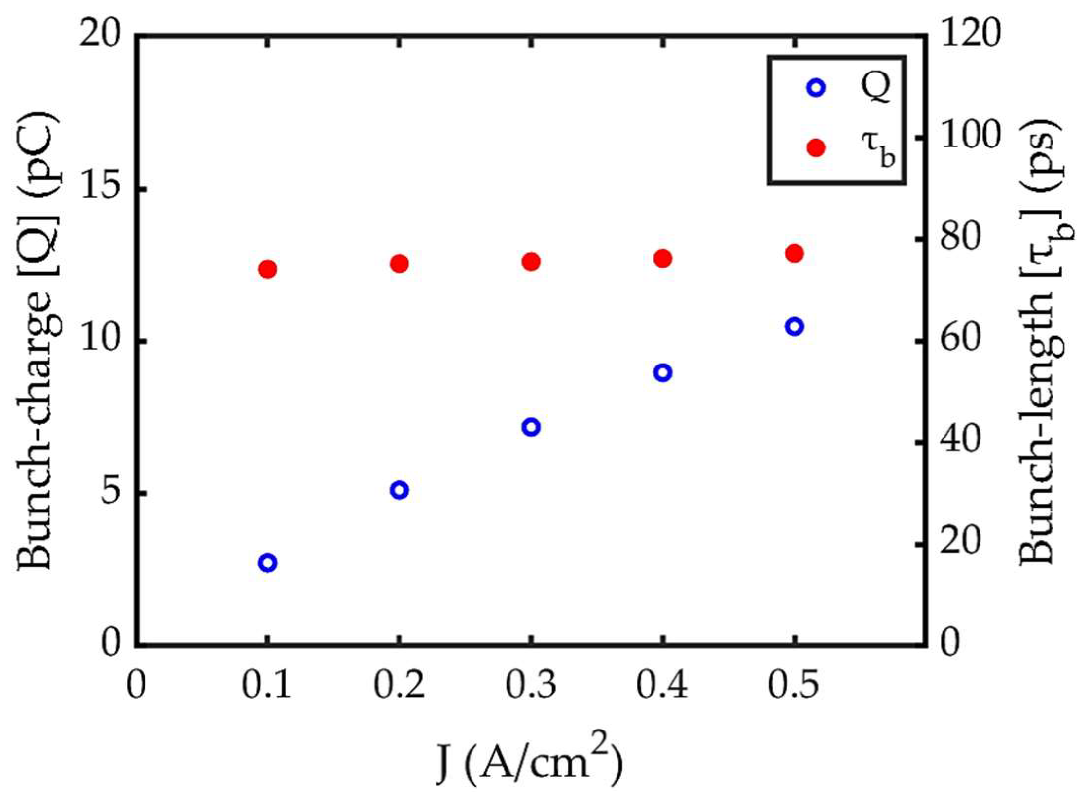
Figure 9.
Longitudinal phase space distribution (a) near cathode (z = 5 µm), and (b) at the grid (z = 160 µm) for
Figure 9.
Longitudinal phase space distribution (a) near cathode (z = 5 µm), and (b) at the grid (z = 160 µm) for
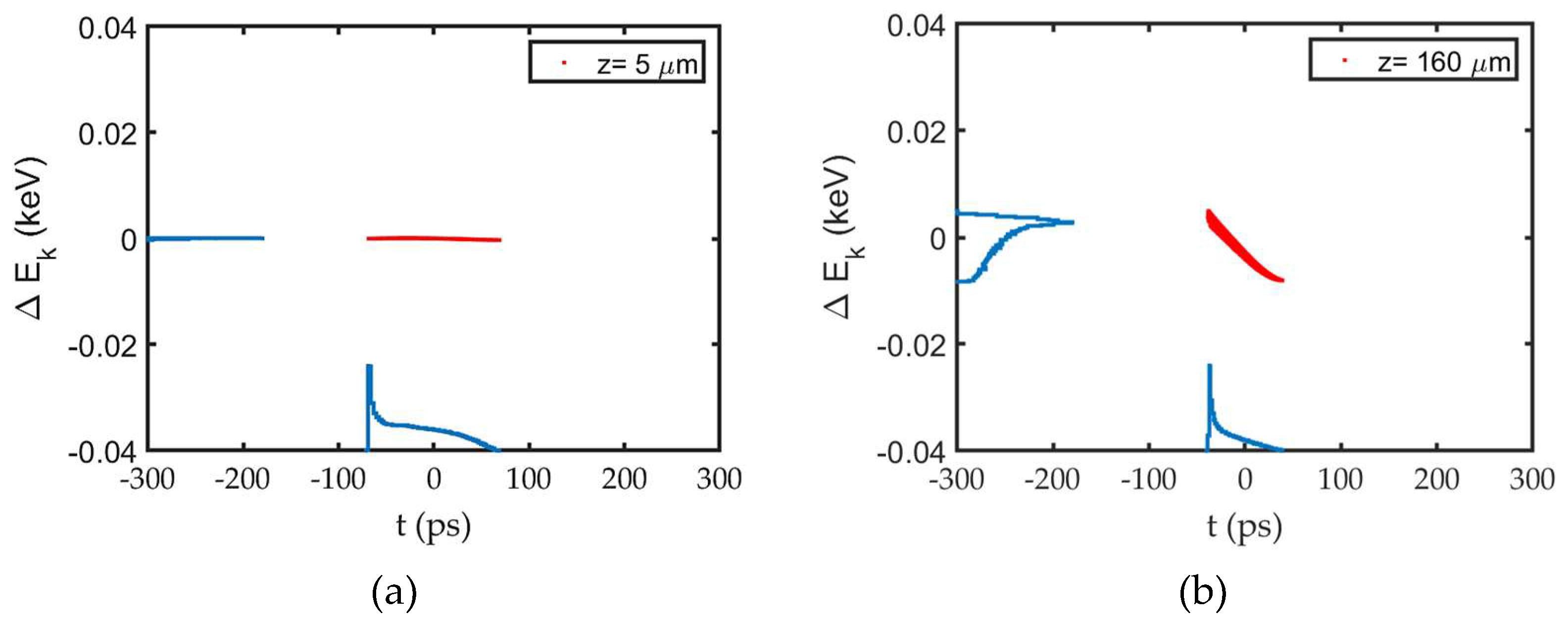
Figure 10.
(a) Bunch-length and (b) bunch-charge at the grid (z = 160 µm) and downstream the anode (z = 40 mm) for different
Figure 10.
(a) Bunch-length and (b) bunch-charge at the grid (z = 160 µm) and downstream the anode (z = 40 mm) for different
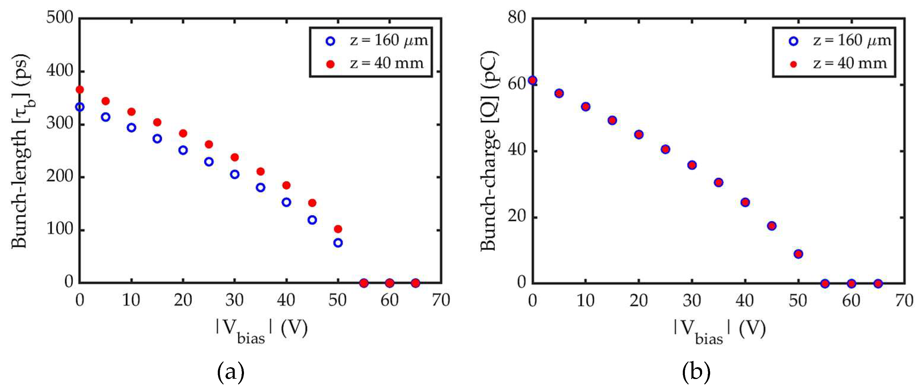
Figure 11.
Longitudinal phase space distribution for with Q =8.96 pC i.e. with space charge at (a) wehnelt position (z = 0.5 mm), (b) middle of the gun geometry (z = 20 mm) and (c) downstream the anode (z = 40 mm).
Figure 11.
Longitudinal phase space distribution for with Q =8.96 pC i.e. with space charge at (a) wehnelt position (z = 0.5 mm), (b) middle of the gun geometry (z = 20 mm) and (c) downstream the anode (z = 40 mm).
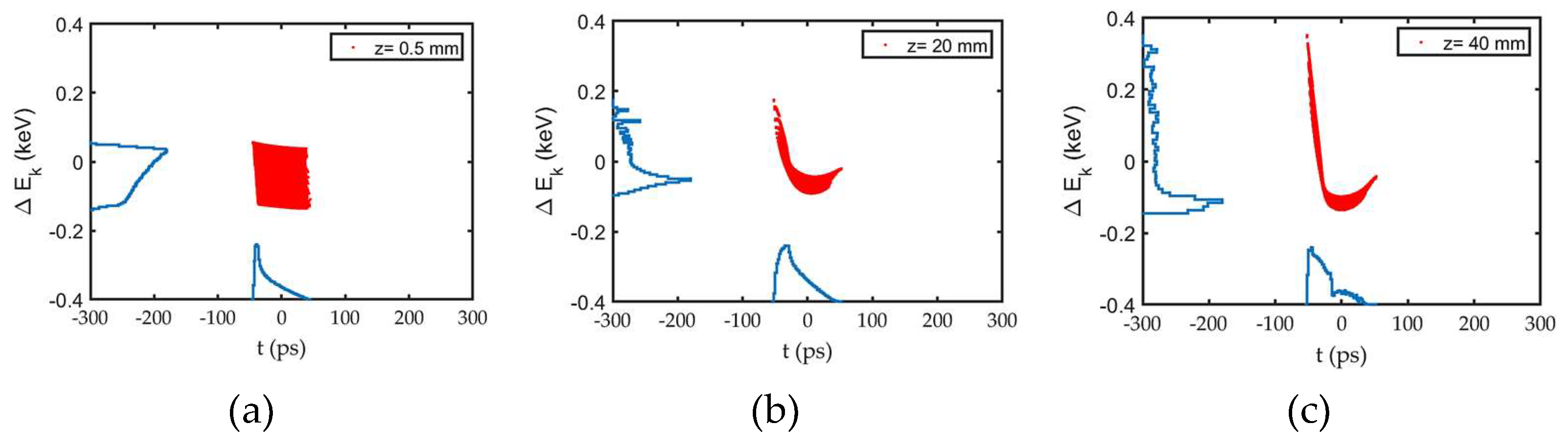
Figure 12.
Longitudinal phase space distribution for without space charge at (a) wehnelt position (z = 0.5 mm), (b) middle of the gun geometry (z = 20 mm) and (c) downstream the anode (z = 40 mm)
Figure 12.
Longitudinal phase space distribution for without space charge at (a) wehnelt position (z = 0.5 mm), (b) middle of the gun geometry (z = 20 mm) and (c) downstream the anode (z = 40 mm)
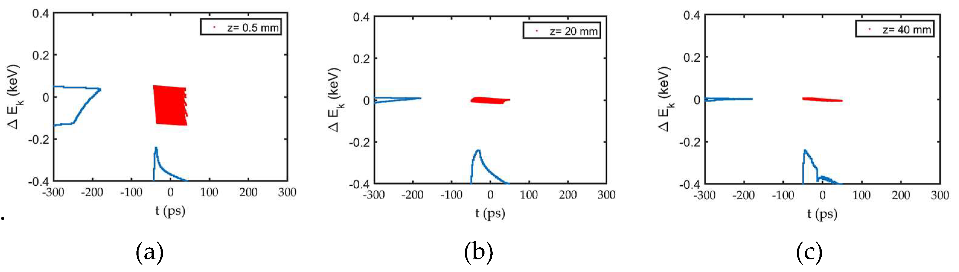
Figure 13.
Longitudinal electric field due to HV along the axis and the along the transverse position of 4mm.
Figure 13.
Longitudinal electric field due to HV along the axis and the along the transverse position of 4mm.
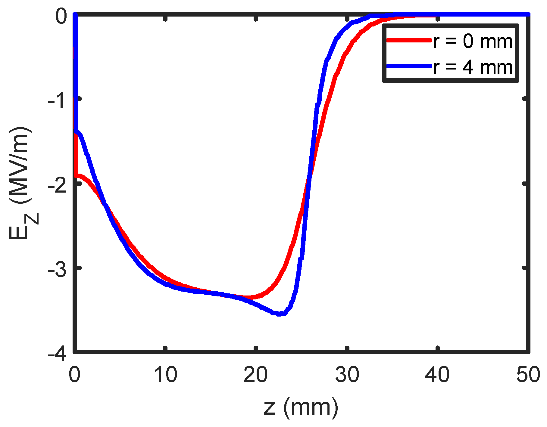
Figure 14.
(a) bunch-length obtained at buncher position (z= 500 mm) for different and (b) longitudinal phase space distribution for the optimal .
Figure 14.
(a) bunch-length obtained at buncher position (z= 500 mm) for different and (b) longitudinal phase space distribution for the optimal .
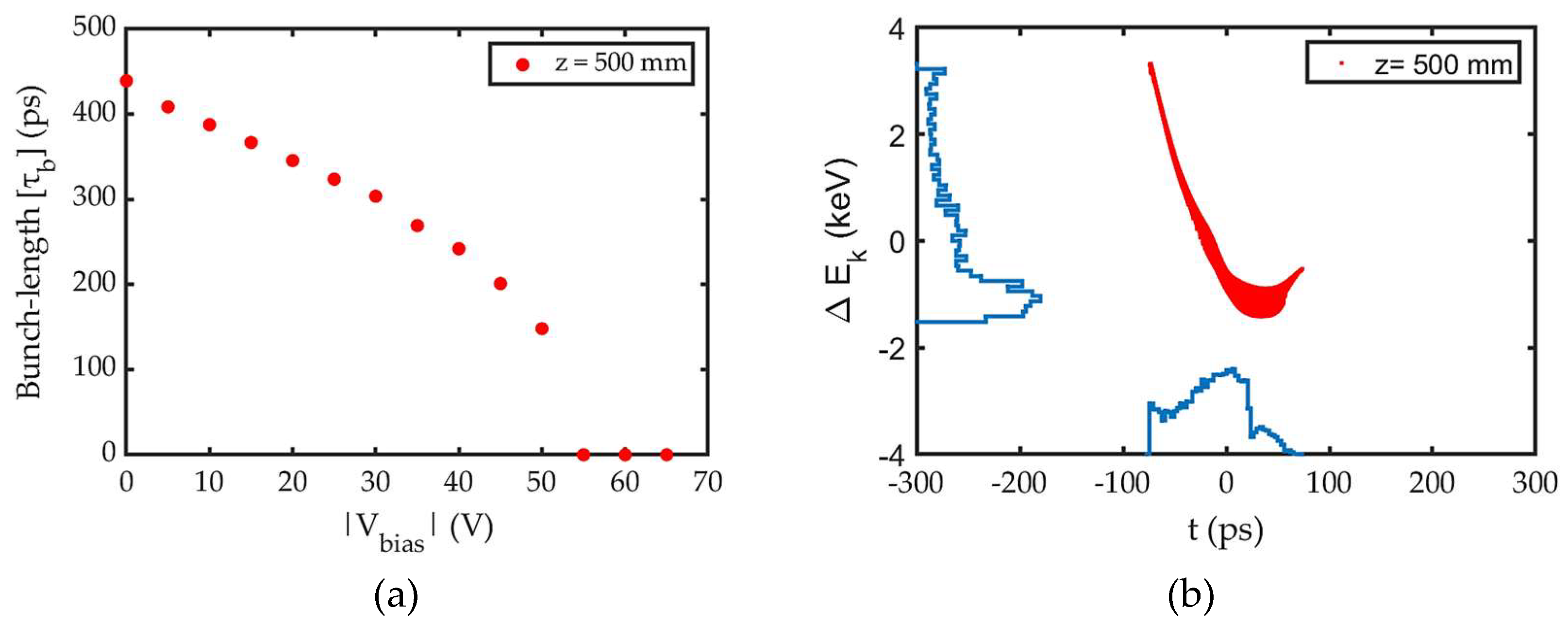
Figure 15.
Transverse slice emittance (red) of the bunch and the distribution of bunch-charge (blue) within the bunch.
Figure 15.
Transverse slice emittance (red) of the bunch and the distribution of bunch-charge (blue) within the bunch.
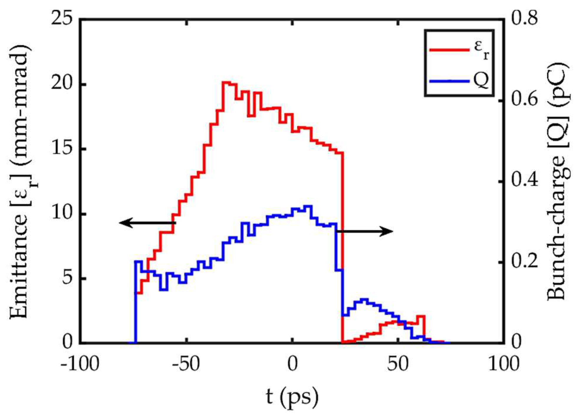
Figure 16.
Longitudinal phase space distribution of the bunch for downstream the 3-cell buncher.
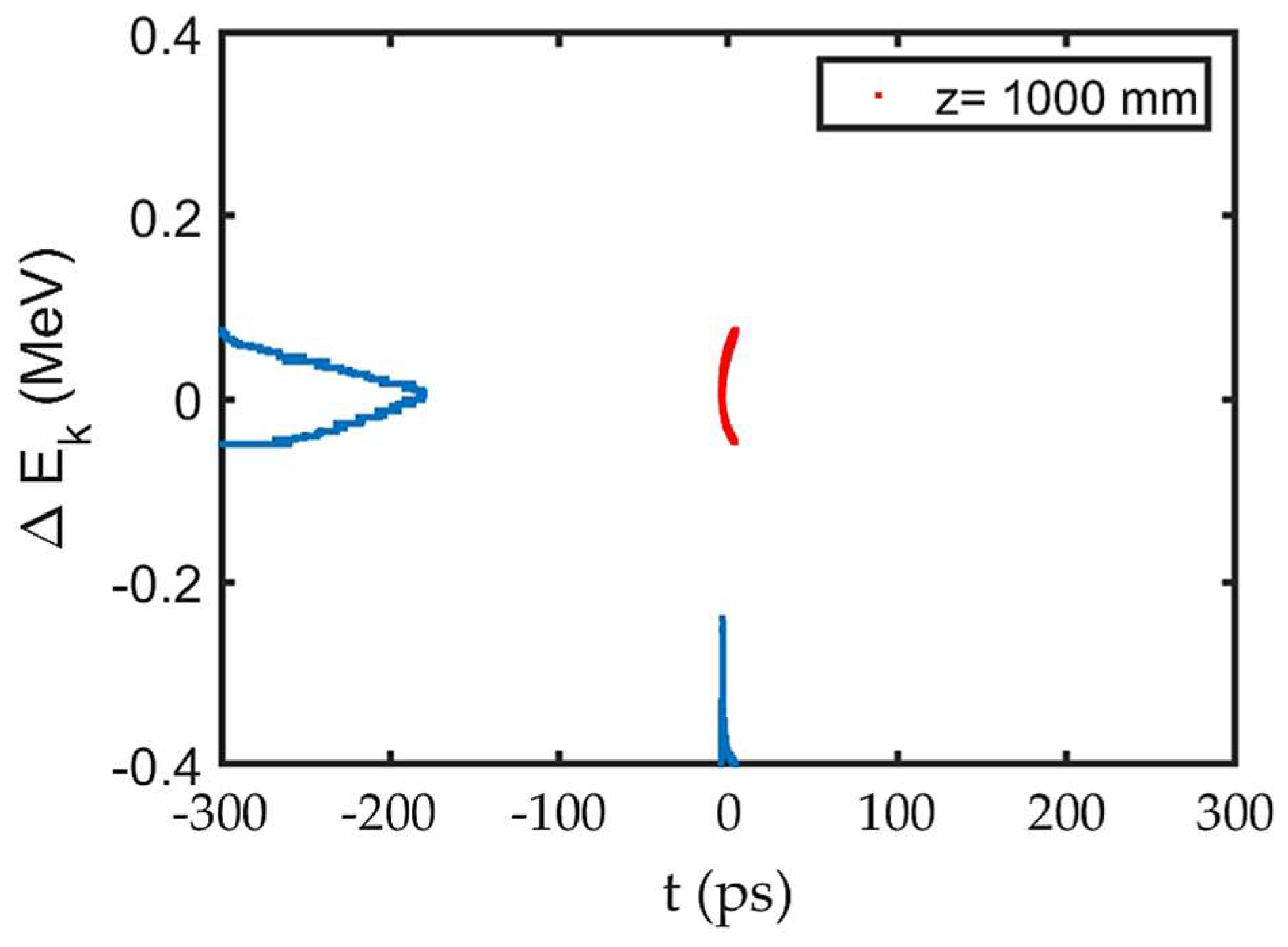
Figure 17.
bunch-length and bunch-charge for different combinition of and resulting into .
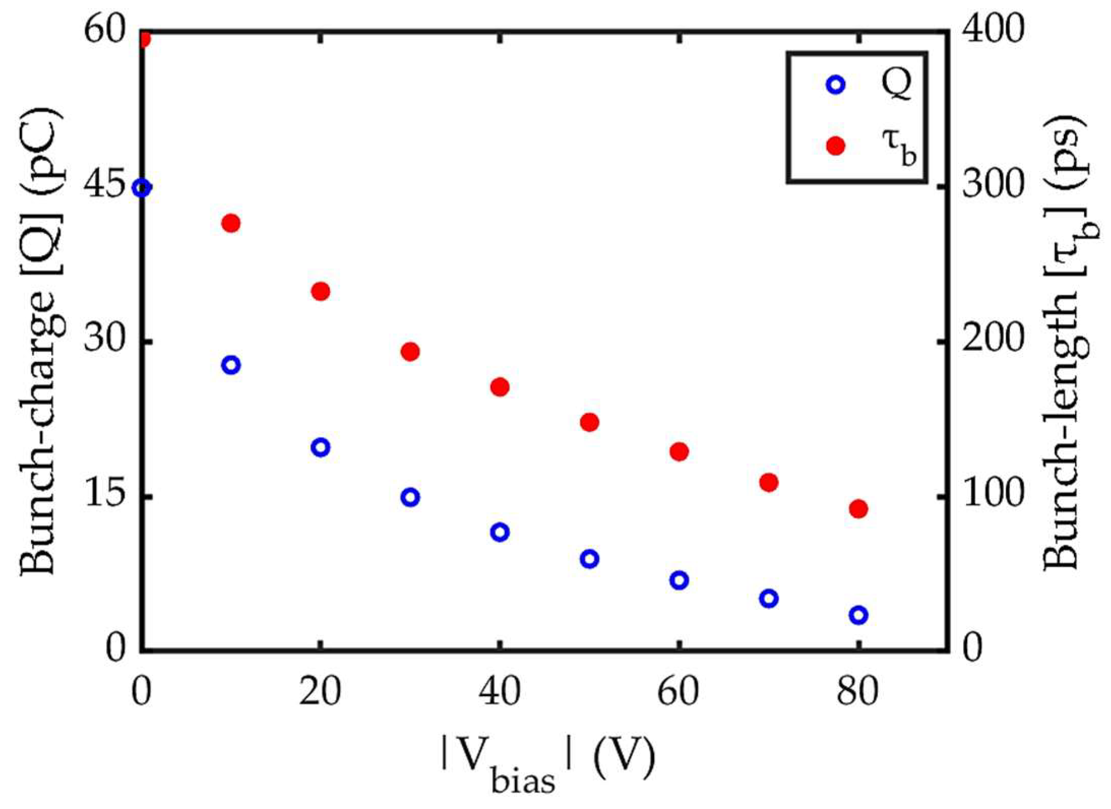
Figure 18.
Emission area for different combinition of and resulting into .
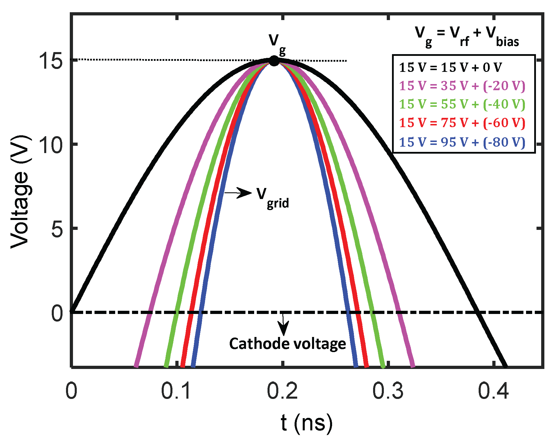

Table 1.
specifications of 1.3 GHz coaxial cavity.
| L | 72.54355 mm |
| a | 4.455 mm |
| d | 160 µm |
Disclaimer/Publisher’s Note: The statements, opinions and data contained in all publications are solely those of the individual author(s) and contributor(s) and not of MDPI and/or the editor(s). MDPI and/or the editor(s) disclaim responsibility for any injury to people or property resulting from any ideas, methods, instructions or products referred to in the content. |
© 2025 by the authors. Licensee MDPI, Basel, Switzerland. This article is an open access article distributed under the terms and conditions of the Creative Commons Attribution (CC BY) license (http://creativecommons.org/licenses/by/4.0/).
Copyright: This open access article is published under a Creative Commons CC BY 4.0 license, which permit the free download, distribution, and reuse, provided that the author and preprint are cited in any reuse.


