
Submitted:
07 May 2025
Posted:
08 May 2025
You are already at the latest version
Abstract
SnSe2, as a prominent member of post-transition metal dichalcogenides, exhibits many intriguing physical phenomena and excellent thermoelectric properties, calling for both fundamental study and potential application in 2D devices. In this article, we realized the molecular beam epitaxial growth of SnSe2 films on √3×√3-Sn reconstructed Si(111) surface. The analysis of reflection high-energy electron diffraction reveal the in-plane lattice orientation as SnSe2[110]//√3-Sn[112]//Si[110]. Besides, the flat morphology of SnSe2 film was identified by scanning tunneling microscopy (STM), implying the relatively strong adsorption effect of √3-Sn/Si(111) substrate to the SnSe2 adsorbates. Subsequently, the interfacial charge transfer was observed by X-ray photoemission spectroscopy. Afterwards, the direct characterization of electronic structures was obtained via angle-resolved photoemission spectroscopy. In addition to proving the presence of interfacial charge transfer again, a new relatively flat in-gap band was found in monolayer and few-layer SnSe2, which was disappeared in multi-layer SnSe2. The interface strain induced partial structural phase transition of thin SnSe2 films is presumed to be the reason. Our results provide important information on characterization and effective modulation of electronic structures of SnSe2 grown on √3-Sn/Si(111), paving the way for the further study and application of SnSe2 in 2D electronic devices.
Keywords:
SnSe2
; electronic structures
; molecular beam epitaxy
; structural phase transition
; angle-resolved photoemission spectroscopy
1. Introduction
Post-transition metal dichalcogenides (PTMCs), composed of III-VA metal elements (Ga, In, Sn, Bi, etc) and chalcogen elements (S, Se, Te), is a new class of layered two-dimensional (2D) materials that intrigued extensive studies recently. In addition to the highly anisotropic lattice structure and unique electronic structures, many outstanding electrochemical, thermoelectric, and optoelectronic properties were observed in PTMCs. Therefore, PTMCs have been applied in many fields like electrochemistry [1,2], electronics [3,4,5], optoelectronics [6,7] and gas sensing [8]. As a prominent member of PTMCs, SnSe2 is an intrinsic layered semiconductor, exhibiting considerable bandgap and excellent thermoelectric properties like ultra-low thermal conductivity and high carrier mobility [9,10]. Together with high abundance and low toxicity of Sn, SnSe2 shows potential applications in optoelectronics [11,12], thermoelectric devices [13], lithium-ion batteries [14] and phase change memory [15].
Besides, intriguing physical properties like charge density wave (CDW), superconductivity, and interfacial polarons were observed in SnSe2 from previous works [1][17,18]. The interface properties of monolayer (ML) SnSe2 could be effectively tuned by choosing different substrates. For examples, a recent study showed that ML and bilayer SnSe2 films grown on Si(111) undergoes a commensurate CDW transition at TC ~ 78 K driven by Fermi surface nesting between symmetry inequivalent electron pockets, forming a corresponding (2×2) superlattice[18]. In addition, the formation of interfacial polarons induced by charge accumulation and electron-phonon coupling between SrTiO3 and SnSe2 was evidenced [17]. Besides, the superconductivity in SnSe2, which can be modulated by cation intercalation [19] and dielectric gating techniques [20], was reported to be enhanced in the epitaxial SnSe2 on graphitized SiC(0001) substrate [16]. However, there are only a few studies on SnSe2 film grown on Si(111), especially the study on direct characterization of band structures is still lacking. In this paper, we synthesize SnSe2 films on Si(111) by molecular beam epitaxy (MBE), and employ in-situ reflection high energy electron diffraction (RHEED), scanning tunneling microscopy (STM), X-ray photoemission spectroscopic (XPS) and angle-resolved photoemission spectroscopy (ARPES) to characterize the atomic and electronic structures of them. We found that the SnSe2 shows layer-by-layer growth mode on -Sn/Si(111) substrate with high-quality of flatness. The interfacial charge transfer effect is observed in the SnSe2 film grown on -Sn/Si(111) substrate. Moreover, an emerging band above the original valence band of bulk SnSe2 is found in the SnSe2 thin film, resulting the reduction of the indirect band gap. This emerging band is suggested to be induced by the interfacial strain driven structural phase transition of the grown SnSe2. Our results provide important information for the further applications of SnSe2 film in 2D electronic devices.
2. Materials and Methods
All the experiments were performed in a combined MBE-STM-ARPES ultra-high vacuum (UHV) system with a base pressure of ~ 2 × 10⁻¹⁰ mbar. At first, to get a clean Si(111)-(7×7) reconstructed surface, a Si(111) substrate (n-doped by P) was initially degassed at , followed by flash-annealing to ~ for 20 cycles. To passivate the dangling bonds of Si(111)-(7×7) surface and enhance the surface diffusion for the growth of SnSe2, we evaporated monolayer of Sn on Si(111)-(7×7) surface at , leading to a well-ordered -Sn recontruction surface on Si(111) (-Sn/Si(111) in the following) surface. Next, the SnSe2 films were grown by co-depositing high-purity Sn (99.99%) and Se (99.99%) from standard Knudsen cells separately, onto the -Sn/Si(111) substrate at . The temperatures of the Sn and Se sources were maintained at and , respectively, keeping the flux ratio at Sn:Se ~1:20. During the film growth, an in-situ RHEED was used for real time monitor and surface structural characterization. After growth, the surface morphology was further characterized by an in-situ room-temperature STM (RT-STM). Subsequently, to investigate the electronic structures, the in-situ low temperature (~10 K) XPS and ARPES were performed by a shared DA30 analyzer (Scienta Omicron AB, Uppsala, Sweden). The monochromatic X-ray of XPS and the ultraviolet light source of ARPES were generated from an Al electrode excitation source (Al Kα, 1486.7 eV) and a Helium lamp with a monochromator (He I, 21.218 eV), respectively.
3. Results and Discussion
The lattice structure of -Sn/Si(111) surface is illustrated in Figure 1a, showing an in-plane 30° rotation and reconstruction of a Sn layer relative to Si(111) surface. Each Sn atom is back-bonded to three Si atoms beneath, with a remaining dangling bond at the surface. Figure 1b presents the lattice structure of T-phase SnSe2 (T-SnSe2). As a typical MX2 of PTMCs, single layer T-SnSe2 consists of two layers of chalcogenides and a layer of transition metal sandwiched between them, presenting a Se-Sn-Se sandwich-like structure. Within the layer, covalent bonding is achieved through Se-Sn, while interlayer stacking is achieved through Se-Se van der Waals interactions, presenting the lattice constants as and [21].
Figure 1c-e present the RHEED patterns of an annealed Si(111)-(7×7) surface, a -Sn/Si(111) surface and a ML SnSe2 film along the Si direction, respectively. Corresponding RHEED patterns along the Si direction are also obtained by 30° rotating the sample in-plane, as shown in Figure 1f-h. From Figure 1c,f, we can see the clearly (7×7) reconstructed patterns of annealed Si surface, which are disappeared and displaced by a new pair of (1×1) diffraction stripes after the -Sn passivation , as shown in Figure 1d,g. Subsequently, from the Figure 1e,h, we can see the new (1×1) diffraction stripes from epitaxial SnSe2 film, which are very clear and sharp, implying the high-quality crystallization.
By performing Lorentz fittings on the corresponding RHEED patterns, we can accurately obtain the (1×1) main diffraction stripe spacings of both substrates and the SnSe2 films (see Figure S1 of the Supplementary Materials for details), on which we can conduct more detailed analysis and calculations. The orientation of the -Sn buffer layer is in-plane rotated by 30° relative to the Si(111), with the calculated lattice constant as , approximately equal to times of . This result is consistent with the previous reports [22,23]. Subsequently, the epitaxial SnSe2 film is rotated by 30° again relative to -Sn/Si surface, resulting in the same in-plane orientation with the Si(111) substrate. Furthermore, the in-plane lattice constant of ML SnSe2 is also obtained as , which is in agreement with the previous report [21].
After growth, we utilized the in-situ STM to investigate the surface morphology of ML SnSe2 grown on -Sn/Si(111), as shown in Figure 1i. Different from three-dimensional island growth mode on graphene substrates [24], the SnSe2 grown on -Sn/Si(111) tends to be layer-by-layer growth mode, which provides the better film flatness. The different growth modes of SnSe2 on two substrates may be attributed to the larger local density of states of -Sn/Si(111) than that of graphene substrate, leading to an increased interface adsorption ability [25,26]. The height of ML SnSe2 is ~0.62 Å [Figure 1j], which is consistent with the previous report [21].
Having determined the lattice structure, we then investigated the chemical states of the SnSe2 film via in-situ XPS. The full XPS spectra of Si(111), -Sn/Si(111) and SnSe2 are shown in the Supplementary Materials Figure S2. Figure 2a presents the Si 2p core-level spectra of the Si(111)-(7×7) surface, -Sn/Si(111) and ML SnSe2 film. For Si(111)-(7×7) surface, the core levels of Si 2p1/2 and Si 2p3/2 orbitals are located at 99.7 eV and 99.1 eV, in accordance with the previous literature [27]. The peaks red-shift by about 0.1 eV compared to the core levels of Si 2p1/2 (99.6 eV) and Si 2p3/2 (99.0 eV) orbitals of the -Sn/Si(111), indicating a charge transfer effect from Sn to Si upon the surface Sn-Si bond formation, which is reasonable since the electronegativity of Si is stronger than that of Sn. Besides, after the growth of ML SnSe2, the core levels of Si 2p1/2 (99.8 eV) and Si 2p3/2 (99.2 eV) again shift toward higher binding energies, which suggests interfacial charge transfer from -Sn/Si(111) substrate to ML SnSe2.
Subsequently, in Figure 2b, the core levels of Sn 3d3/2 (493.3 eV) and 3d5/2 (484.9 eV) orbitals of -Sn/Si(111) exhibit obvious blue-shift compared to the core levels of Sn 3d3/2 (494.6 eV) and 3d5/2 (486.2 eV) orbitals of ML SnSe2. This shift can be explained by the much stronger bond polarity of Sn-Se than that of Sn-Si, which leads to the weakened screening to the Coulomb potential created by the positive core of Sn, and finally resulting in the higher binding energies of the remaining electrons. Besides, in Figure 2c the core levels of Se 3d orbitals of ML SnSe2 split into two sets, Se1 3d3/2 (54.6 eV), Se1 3d5/2 (53.7 eV) and Se2 3d3/2 (55.0 eV), Se2 3d5/2 (54.2 eV), respectively. The splitting of Se 3d orbitals implies the presence of two nonequivalent chemical environments of Se atoms in ML SnSe2. This can be attributed to that the bottom layer of Se atoms is adjacent to √3-Sn surface, while the top layer of Se atoms is located at the top surface of SnSe2.
To further investigate the interface effect, we characterized the electronic structures of SnSe2/-Sn/Si(111) system via in-situ ARPES. Figure 3 shows the electronic structures of Si(111)-(7×7) and -Sn/Si(111) surface. The constant energy mappings near the Fermi level of the Si(111)-(7×7) and -Sn/Si(111) surface clearly display the six-fold symmetry and the relative 30° rotation with respect to each other [Figure 3b,c], in accordance with the corresponding schematic of Brillouin zone (BZ) illustrated in Figure 3(a). The band structure of Si(111)-(7×7) surface is shown in Figure 3d, with the intensity enhanced zoom-in spectra plotted at the bottom panel of Figure 3e for more detailed observation. Three surface states marked as S1, S2 and S3 can be clearly observed, in agreement with the previous literature [28]. The S3 is induced by the back bonds of the (7×7) reconstruction, showing the obvious band dispersion with its maximum located at about −1.8 eV. The nearly flat S2, induced by the rest-atoms, is located at about −0.9 eV, while the S1, induced by the adatoms of the surface reconstruction, lying near the Fermi level.
The band structure of -Sn/Si(111) surface and its zoom-in spectra with enhanced intensity are plotted in Figure 3f and the top panel of Figure 3e, respectively. The surface states S2' is located at −1~−2 eV, and the minimum of surface states S1' is located at −0.7 eV. The S2’ and S1’ are attributed to the three back bonds with Si and the one remaining dangling bond of each Sn adatom, respectively [29,30]. Our results indicate the well processed substrate, on which the SnSe2 films can be grown with high-quality of flatness and crystallization.
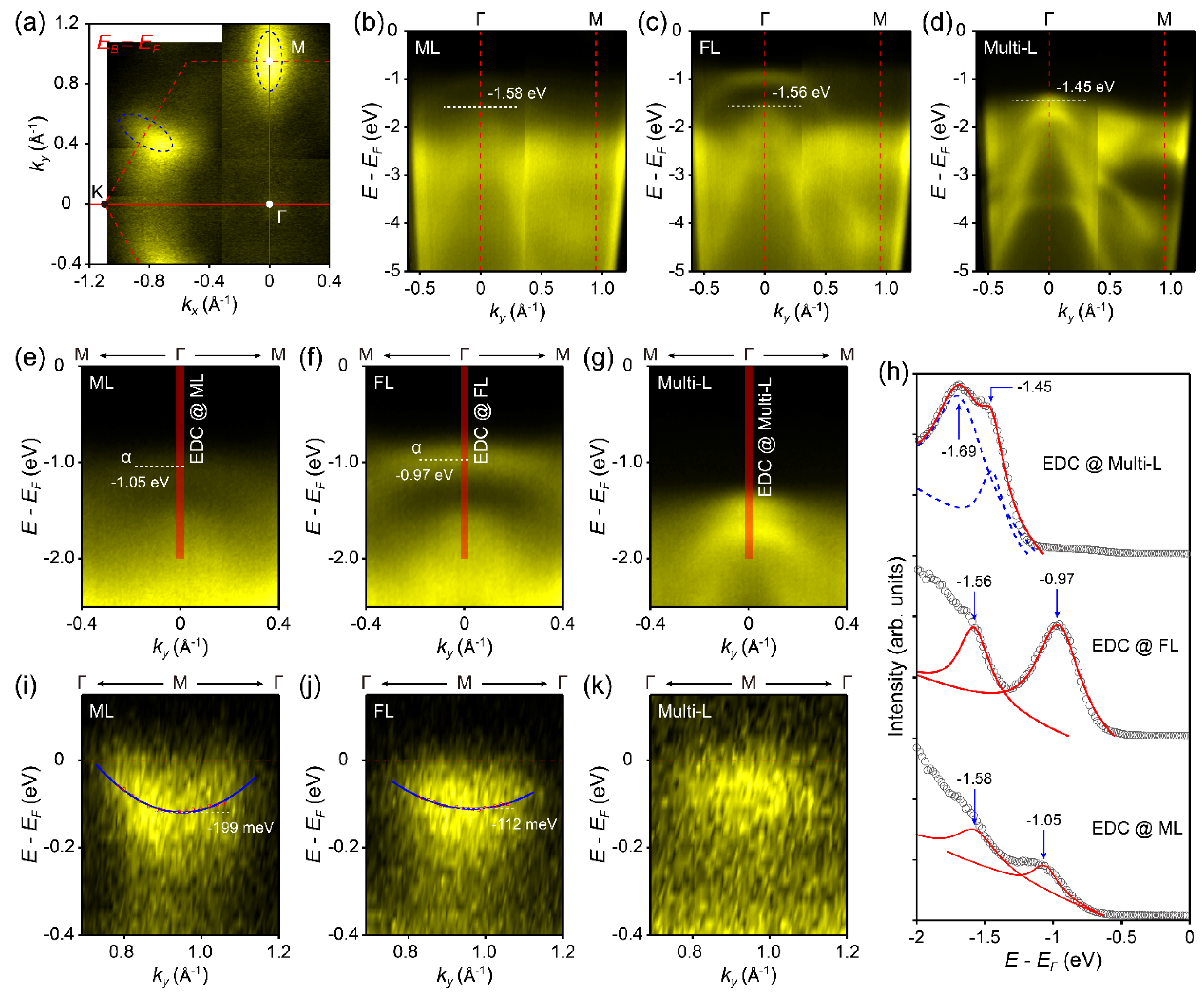
Finally, we investigated the electronic structures of SnSe2 films grown on -Sn/Si(111) surface, as shown in Figure 4. Recent first-principles calculations and ARPES study of SnSe2 showed that bulk SnSe2 possesses an indirect band gap of ~1.07 eV, whose conduction band minimum (CBM) and valence band maximum (VBM) are located along the M-L and Γ-M (K) directions, respectively [31,32]. In contrast, ML SnSe2 film exhibits an indirect band gap of ~1.69 eV, with CBM and VBM located at the M and Γ points, respectively [32]. The increased band gap of ML SnSe2 is attributed to quantum confinement of electrons in quasi-2D samples and the reduction of the screening. The CBM of both ML and bulk SnSe2 are higher than Fermi level, making it difficult to be characterized directly via ARPES in pristine SnSe2.
Figure 4a is the constant energy mapping taken near the Fermi level of ML SnSe2, presenting clear sixfold symmetry, with electron pockets centered at the M points of BZ. It is quite similar to that of the potassium(K)-doped SnSe2 single crystals, suggesting the charge transfer from the -Sn/Si(111) substrate to the grown SnSe2 film. Besides, the CBM of different layers of SnSe2 are obtained from energy distribution curve (EDC) fittings, as shown in Figure S3. It can be clearly seen that all the CBM features appear near the Fermi level at the M point, shifting from −199 meV in ML SnSe2 to −112 meV in few-layer (FL) SnSe2 (the thickness of FL SnSe2 is estimated to be ~3 ML), and finally to the edge of the Fermi level in multi-layer (Multi-L, the estimated thickness is about ~6 ML) SnSe2 [Figure 4i-k]. The upward shift of CBM with the increase of layers again confirms the interfacial charge transfer scenario.
Furthermore, the ARPES spectra of ML, FL and Mult-L SnSe2 along the Γ-M direction are plotted in Figure 4b-d, respectively. The VBM are all located at the Γ point. For more detailed observation, the zoom-in ARPES spectra near the VBM around the Γ point and corresponding EDCs along the red lines are illustrated in Figure 4e-g,h. Intriguingly, we note that a new band α above the original VBM of bulk SnSe2 emerges in the ML and FL SnSe2 films, which disappears in the Mult-L SnSe2. The emerging α band can be better resolved in the second-derivative spectra, as shown in Figure S4. From the EDC fittings in Figure 4h, the maximum of the α band is located at −1.05 eV and −0.97 eV in ML and FL SnSe2, respectively, leading to the reduced band gaps as 0.85 eV in both of them. The position as well as the relatively flat dispersion of α band are quite similar to the top valence band of H phase SnSe2 (H-SnSe2), which was characterized and marked as ‘7/8’ band in a previous literature [33]. Moreover, a recent first-principle calculation showed a reduced band gap of H-SnSe2 compared to T-SnSe2, in accordance with our ARPES results[34]. Therefore, we believe that the newly emerged energy band α would be attributed to the presence of a small amount of H-SnSe2 formed in ML and FL SnSe2. Indeed, a pressure induced structural phase transition to H-SnSe2 was reported before[35]. Therefore, we assume that the interfacial strain from -Sn/Si(111) substrate would be the main reason for the emergence of H-SnSe2, which vanishes gradually as the film become thicker. Furthermore, the indistinct band structures of ML and FL SnSe2, contrary to the clear band structures in Multi-L SnSe2, also provides evidence for our assumption, since the band structures of both T-SnSe2 and H-SnSe2 can be detected by ARPES and eventually overlap together in the spectra, as shown in Figure 4b,c.
4. Conclusions
In summary, we have realized the MBE growth of SnSe2 films on -Sn passivated Si(111) substrate. The analysis of RHEED patterns demonstrate the successful growth and the same in-plane lattice orientation of the grown SnSe2 with Si(111) substrate, whereas the Sn buffer layer conducts a reconstruction with in-plane rotation by 30° relative to both Si(111) and SnSe2. Besides, the layer-by-layer growth mode of SnSe2 identified by STM indicates the relatively strong adsorption effect of -Sn/Si(111) on SnSe2 adsorbates. Subsequently, from the XPS measurements, we observed the interfacial charge transfer from substrate to SnSe2, which was further confirmed in the ARPES measurements. Moreover, a new valence band α located above the original VBM of bulk SnSe2 emerges in the ML and FL SnSe2 films, which disappears in the Multi-layer SnSe2 film. We attribute it to the partial T→H structural phase transition of thin SnSe2 films grown on -Sn/Si(111) substrate, probably driven by the interfacial strain. The direct characterizations of electronic structures of SnSe2 films, as well as the layer-dependent structural transition, along with the effective band modulation, provide significant and important information for the further applications of SnSe2 films in 2D electronic devices.
Supplementary Materials
The following supporting information can be downloaded at the website of this paper posted on Preprints.org., A. Method for calculating lattice constants from RHEED patterns; B. Full XPS spctra; C. EDCs fitting for determining the CBMs; D. Second-derivative ARPES spectra.
Author Contributions
Conceptualization, Y.Z.; methodology, Z.L., Q.T., K.W., Y.M., Z.F., X.Q., Q.M., C.W., and Y.Z.; software, Y.Z.; validation, Z.L., Q.T., K.W., Y.M. and Y.Z.; formal analysis, Z.L., Q.T., K.W., Y.M. and Y.Z.; investigation, Z.L. and Q.T.; resources, Y.Z.; data curation, Z.L., Q.T., K.W., Y.M. and Y.Z.; writing—original draft preparation, Z.L.; writing—review and editing, Y.Z.; visualization, Z.L., Q.T., K.W. and Y.M.; supervision, C.W. and Y.Z.; project administration, Y.Z.; funding acquisition, Y.Z.. All authors have read and agreed to the published version of the manuscript.
Funding
This research was funded by the National Natural Science Foundation of China (No. 92165205), the Fundamental Research Funds for the Central University (No. 0204/14380228), the Fundamental Research Program of Natural Science Foundation of Jiangsu Province (BK20243011), and the Natural Science Foundation of Hunan Province of China (No. 2024jj6009).
Institutional Review Board Statement
Not applicable.
Informed Consent Statement
Not applicable.
Data Availability Statement
Dataset available on request from the authors.
Conflicts of Interest
The authors declare no conflicts of interest.
Abbreviations
The following abbreviations are used in this manuscript:
| PTMCs | Post-transition metal dichalcogenides |
| CDW | Charge density wave |
| ML | Monolayer |
| MBE | Molecular beam epitaxy |
| RHEED | Reflection high energy electron diffraction |
| XPS | X-ray photoemission spectroscopy |
| ARPES | Angle-resolved photoemission spectroscopy |
| UHV | Ultra-high-vacuum |
| BZ | Brillouin zone |
| CBM | Conduction band minimum |
| VBM | Valence band maximum |
| EDC | Energy distribution curve |
| FL | Few-layer |
| Multi-L | Multi-layer |
References
- Tan, S.M.; Chua, C.K.; Sedmidubský, D.; Sofer, Z.B.; Pumera, M. Electrochemistry of layered GaSe and GeS: Applications to ORR, OER and HER. Physical Chemistry Chemical Physics 2016, 18, 1699. [Google Scholar] [CrossRef] [PubMed]
- Wang, Y.; Szökölová, K.; Nasir, M.Z.M.; Sofer, Z.; Pumera, M. Electrochemistry of Layered Semiconducting AIIIBVI Chalcogenides: Indium Monochalcogenides (InS, InSe, InTe). ChemCatChem 2019, 11, 2634. [Google Scholar] [CrossRef]
- Sucharitakul, S.; Goble, N.J.; Kumar, U.R.; Sankar, R.; Bogorad, Z.A.; Chou, F.C.; Chen, Y.T.; Gao, X.P.A. Intrinsic Electron Mobility Exceeding 103 cm2/(V s) in Multilayer InSe FETs. Nano Letters 2015, 15, 3815. [Google Scholar] [CrossRef]
- Xu, K.; Yin, L.; Huang, Y.; Shifa, T.A.; Chu, J.; Wang, F.; Cheng, R.; Wang, Z.; He, J. Synthesis, properties and applications of 2D layered MIIIXVI (M = Ga, In; X = S, Se, Te) materials. Nanoscale 2016, 8, 16802. [Google Scholar] [CrossRef] [PubMed]
- Sucharitakul, S.; Goble, N.J.; Kumar, U.R.; Sankar, R.; Bogorad, Z.A.; Chou, F.-C.; Chen, Y.-T.; Gao, X.P.A. Intrinsic Electron Mobility Exceeding 103 cm2/(Vs) in Multilayer InSe FETs. Nano Letters 2015, 15, 3815. [Google Scholar] [CrossRef]
- Hu, P.; Wen, Z.; Wang, L.; Tan, P.; Xiao, K. Synthesis of few-layer GaSe nanosheets for high performance photodetectors. ACS Nano 2012, 6, 5988. [Google Scholar] [CrossRef]
- Hu, P.; Zhang, J.; Yoon, M.; Qiao, X.-F.; Zhang, X.; Feng, W.; Tan, P.; Zheng, W.; Liu, J.; Wang, X.; Idrobo, J.C.; Geohegan, D.B.; Xiao, K. Highly sensitive phototransistors based on two-dimensional GaTe nanosheets with direct bandgap. Nano Research 2014, 7, 694. [Google Scholar] [CrossRef]
- Marvan, P.; Mazánek, V.; Sofer, Z. Shear-force exfoliation of indium and gallium chalcogenides for selective gas sensing applications. Nanoscale 2019, 11, 4310. [Google Scholar] [CrossRef]
- Li, G.; Ding, G.; Gao, G. Thermoelectric properties of SnSe2 monolayer. Journal of Physics: Condensed Matter 2017, 29, 015001. [Google Scholar]
- Shafique, A.; Samad, A.; Shin, Y.-H. Ultra low lattice thermal conductivity and high carrier mobility of monolayer SnS2 and SnSe2: a first principles study. Physical Chemistry Chemical Physics 2017, 19, 20677. [Google Scholar] [CrossRef]
- Huang, Y.; Xu, K.; Wang, Z.; Shifa, T.A.; Wang, Q.; Wang, F.; Jiang, C.; He, J. Designing the shape evolution of SnSe2 nanosheets and their optoelectronic properties. Nanoscale 2015, 7, 17375. [Google Scholar] [CrossRef]
- Zhou, X.; Gan, L.; Tian, W.; Zhang, Q.; Jin, S.; Li, H.; Bando, Y.; Golberg, D.; Zhai, T. Ultrathin SnSe2 Flakes Grown by Chemical Vapor Deposition for High-Performance Photodetectors. Advanced Materials 2015, 27, 8035. [Google Scholar] [CrossRef] [PubMed]
- Luo, Y.; Zheng, Y.; Luo, Z.; Hao, S.; Du, C.; Liang, Q.; Li, Z.; Khor, K.A.; Hippalgaonkar, K.; Xu, J.; Yan, Q.; Wolverton, C.; Kanatzidis, M.G. n-Type SnSe2 Oriented-Nanoplate-Based Pellets for High Thermoelectric Performance. Advanced Energy Materials 2018, 8, 1702167. [Google Scholar] [CrossRef]
- Choi, J.; Jin, J.; Jung, I.G.; Kim, J.M.; Kim, H.J.; Son, S.U. SnSe2 nanoplate–graphene composites as anode materials for lithium ion batteries. Chemical Communications 2011, 47, 5241. [Google Scholar] [CrossRef] [PubMed]
- Wang, R.Y.; Caldwell, M.A.; Jeyasingh, R.G.D.; Aloni, S.; Shelby, R.M.; Wong, H.S.P.; Milliron, D.J. Electronic and optical switching of solution-phase deposited SnSe2 phase change memory material. Journal of Applied Physics 2011, 109, 113506. [Google Scholar] [CrossRef]
- Zhang, Y.-M.; Fan, J.-Q.; Wang, W.-L.; Zhang, D.; Wang, L.; Li, W.; He, K.; Song, C.-L.; Ma, X.-C.; Xue, Q.-K. Observation of interface superconductivity in a SnSe2 epitaxial graphene van der Waals heterostructure. Physical Review B 2018, 98, 220508. [Google Scholar] [CrossRef]
- Mao, Y.; Ma, X.; Wu, D.; Lin, C.; Shan, H.; Wu, X.; Zhao, J.; Zhao, A.; Wang, B. Interfacial Polarons in van der Waals Heterojunction of Monolayer SnSe2 on SrTiO3 (001). Nano Letters 2020, 20, 8067. [Google Scholar] [CrossRef]
- Wang, S.-Z.; Zhang, Y.-M.; Fan, J.-Q.; Ren, M.-Q.; Song, C.-L.; Ma, X.-C.; Xue, Q.-K. Charge density waves and Fermi level pinning in monolayer and bilayer SnSe2. Physical Review B 2020, 102, 241408. [Google Scholar] [CrossRef]
- Wu, H.; Li, S.; Susner, M.; Kwon, S.; Kim, M.; Haugan, T.; Lv, B. Spacing dependent and cation doping independent superconductivity in intercalated 1T 2D SnSe2. 2D Materials 2019, 6, 045048. [Google Scholar] [CrossRef]
- Zeng, J.; Liu, E.; Fu, Y.; Chen, Z.; Pan, C.; Wang, C.; Wang, M.; Wang, Y.; Xu, K.; Cai, S.; Yan, X.; Wang, Y.; Liu, X.; Wang, P.; Liang, S.-J.; Cui, Y.; Hwang, H.Y.; Yuan, H.; Miao, F. Gate-Induced Interfacial Superconductivity in 1T-SnSe2. Nano Letters 2018, 18, 1410. [Google Scholar] [CrossRef]
- Schlüter, M.; Cohen, M.L. Valence-band density of states and chemical bonding for several non-transition-metal layer compounds: SnSe2, PbI2, BiI3, and GaSe. Physical Review B 1976, 14, 424. [Google Scholar] [CrossRef]
- Zhachuk, R.A.; Rogilo, D.I.; Petrov, A.S.; Sheglov, D.V.; Latyshev, A.V.; Colonna, S.; Ronci, F. Atomic structure of a single step and dynamics of Sn adatoms on the Si(111)-√3×√3-Sn surface. Physical Review B 2021, 104, 125437. [Google Scholar] [CrossRef]
- Wu, X.; Ming, F.; Smith, T.S.; Liu, G.; Ye, F.; Wang, K.; Johnston, S.; Weitering, H.H. Superconductivity in a Hole-Doped Mott-Insulating Triangular Adatom Layer on a Silicon Surface. Physical Review Letters 2020, 125, 117001. [Google Scholar] [CrossRef] [PubMed]
- Zhang, Y.; Wang, C.; Tian, Q.; Meng, Q.; Zong, J.; Zhang, Y. Epitaxial Growth of Monolayer SnSe2 Films on Gd-Intercalated Quasi-Free-Standing Monolayer Graphene with Enhanced Interface Adsorption. The Journal of Physical Chemistry C 2022, 126, 5751. [Google Scholar] [CrossRef]
- Jiang, P.; Ma, X.; Ning, Y.; Song, C.; Chen, X.; Jia, J.-F.; Xue, Q.-K. Quantum Size Effect Directed Selective Self-Assembling of Cobalt Phthalocyanine on Pb(111) Thin Films. Journal of the American Chemical Society 2008, 130, 7790. [Google Scholar] [CrossRef] [PubMed]
- Huttmann, F.; Martínez-Galera, A.J.; Caciuc, V.; Atodiresei, N.; Schumacher, S.; Standop, S.; Hamada, I.; Wehling, T.O.; Blügel, S.; Michely, T. Tuning the van der Waals Interaction of Graphene with Molecules via Doping. Physical Review Letters 2015, 115, 236101. [Google Scholar] [CrossRef]
- Barr, T.L. An XPS study of Si as it occurs in adsorbents, catalysts, and thin films. Applications of Surface Science 1983, 15, 1. [Google Scholar] [CrossRef]
- Sheverdyaeva, P.M.; Mahatha, S.K.; Ronci, F.; Colonna, S.; Moras, P.; Satta, M.; Flammini, R. Signature of surface periodicity in the electronic structure of Si(1 1 1)-(7 × 7). Journal of physics. Condensed matter : an Institute of Physics journal 2017, 29, 215001. [Google Scholar] [CrossRef]
- Kinoshita, T.; Kono, S.; Sagawa, T. Angle-resolved photoelectron-spectroscopy study of the Si(111) √3×√3-Sn surface: Comparison with Si(111) √3×√3-Al, -Ga, and -In surfaces. Physical Review B 1986, 34, 3011. [Google Scholar] [CrossRef]
- Lobo, J.; Tejeda, A.; Mugarza, A.; Michel, E.G. Electronic structure of Sn/Si(111)-√3×√3R30° as a function of Sn coverage. Physical Review B 2003, 68, 235332. [Google Scholar] [CrossRef]
- Lochocki, E.B.; Vishwanath, S.; Liu, X.; Dobrowolska, M.; Furdyna, J.; Xing, H.G.; Shen, K.M. Electronic structure of SnSe2 films grown by molecular beam epitaxy. Applied Physics Letters 2019, 114, 091602. [Google Scholar] [CrossRef]
- Gonzalez, J.M.; Oleynik, I.I. Layer-dependent properties of ${\mathbf{SnS}}_{2}$ and ${\mathbf{SnSe}}_{2}$ two-dimensional materials. Physical Review B 2016, 94, 125443. [Google Scholar] [CrossRef]
- Bertrand, Y.; Solal, F.; Levy, F. Experimental band structure of 2H-SnSe2 by synchrotron radiation photoemission spectroscopy. Journal of Physics C: Solid State Physics 1984, 17, 2879. [Google Scholar] [CrossRef]
- Brizolla, G.M.S.; Chaves, A.J.; Teles, L.K.; Guilhon, I.; Junior, J.M.P. Electrically controlled charge qubit in van der Waals heterostructures: From ab initio calculation to tight-binding models. Physical Review B 2024, 109, 125416. [Google Scholar] [CrossRef]
- Ge, B.; Li, C.; Lu, W.; Ye, H.; Li, R.; He, W.; Wei, Z.; Shi, Z.; Kim, D.; Zhou, C.; Zhu, M.; Wuttig, M.; Yu, Y. Dynamic Phase Transition Leading to Extraordinary Plastic Deformability of Thermoelectric SnSe2 Single Crystal. Advanced Energy Materials 2023, 13, 2300965. [Google Scholar] [CrossRef]
Figure 1.
a) Top-view lattice structure of -Sn/Si(111) reconstruction. (b) Top-view lattice structure of a ML T-SnSe2. (c-e) RHEED patterns of (c) Si(111)-(7×7) surface, (d) -Sn/Si(111) surface and (e) ML SnSe2 film along the Si direction, respectively. (f-h) RHEED patterns of (f) Si(111)-(7×7) surface, (g) -Sn/Si(111) surface and (h) ML SnSe2 film along the Si direction, respectively. (i, j) (i) STM topography of ML SnSe2 film and (j) the corresponding height profiles along the green line in (i).
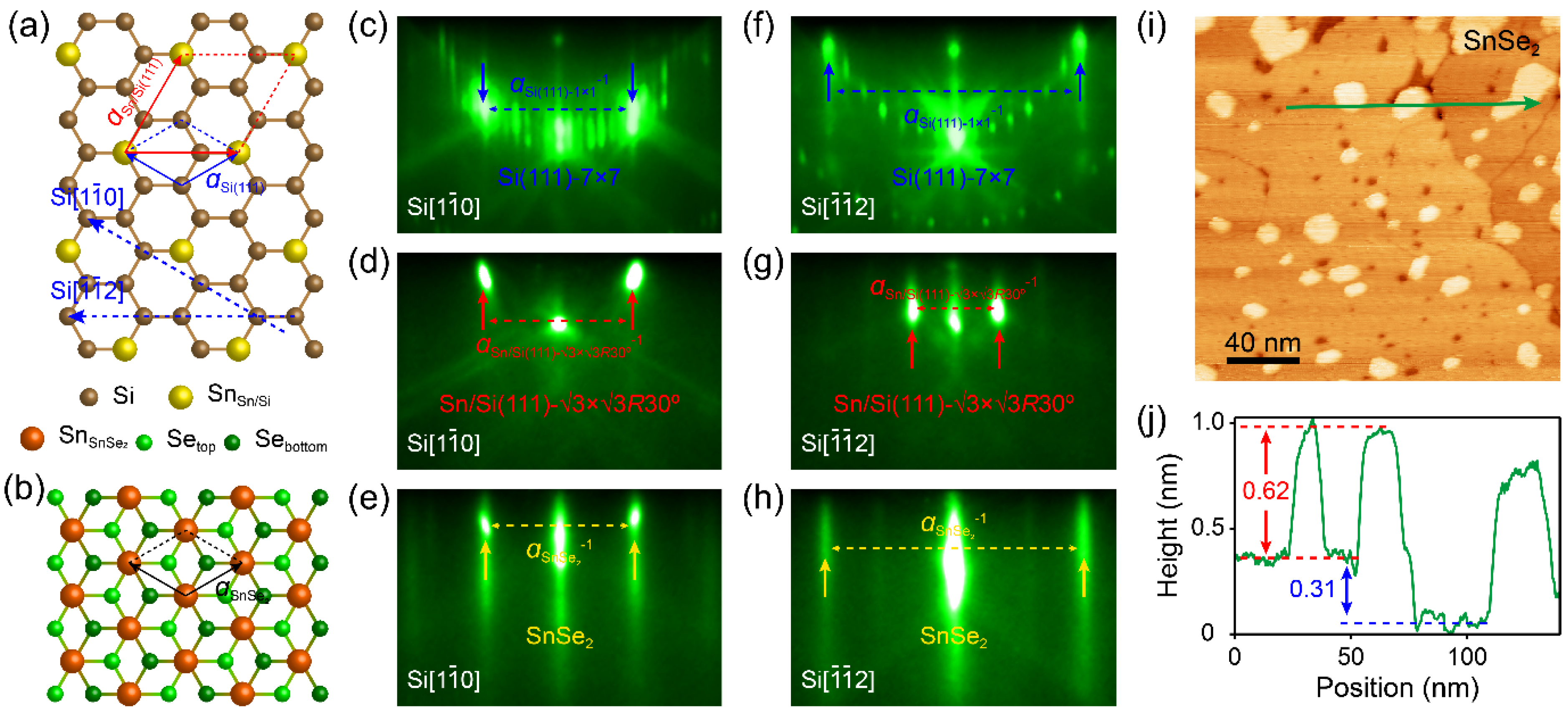
Figure 2.
(a) XPS spectra around Si 2p orbitals of the Si(111)-(7×7) surface, -Sn/Si(111), and ML SnSe2. (b) XPS spectra around Sn 3d orbitals of the -Sn/Si(111) and ML SnSe2. (c) XPS spectra around Se 3d orbitals of the ML SnSe2.
Figure 2.
(a) XPS spectra around Si 2p orbitals of the Si(111)-(7×7) surface, -Sn/Si(111), and ML SnSe2. (b) XPS spectra around Sn 3d orbitals of the -Sn/Si(111) and ML SnSe2. (c) XPS spectra around Se 3d orbitals of the ML SnSe2.
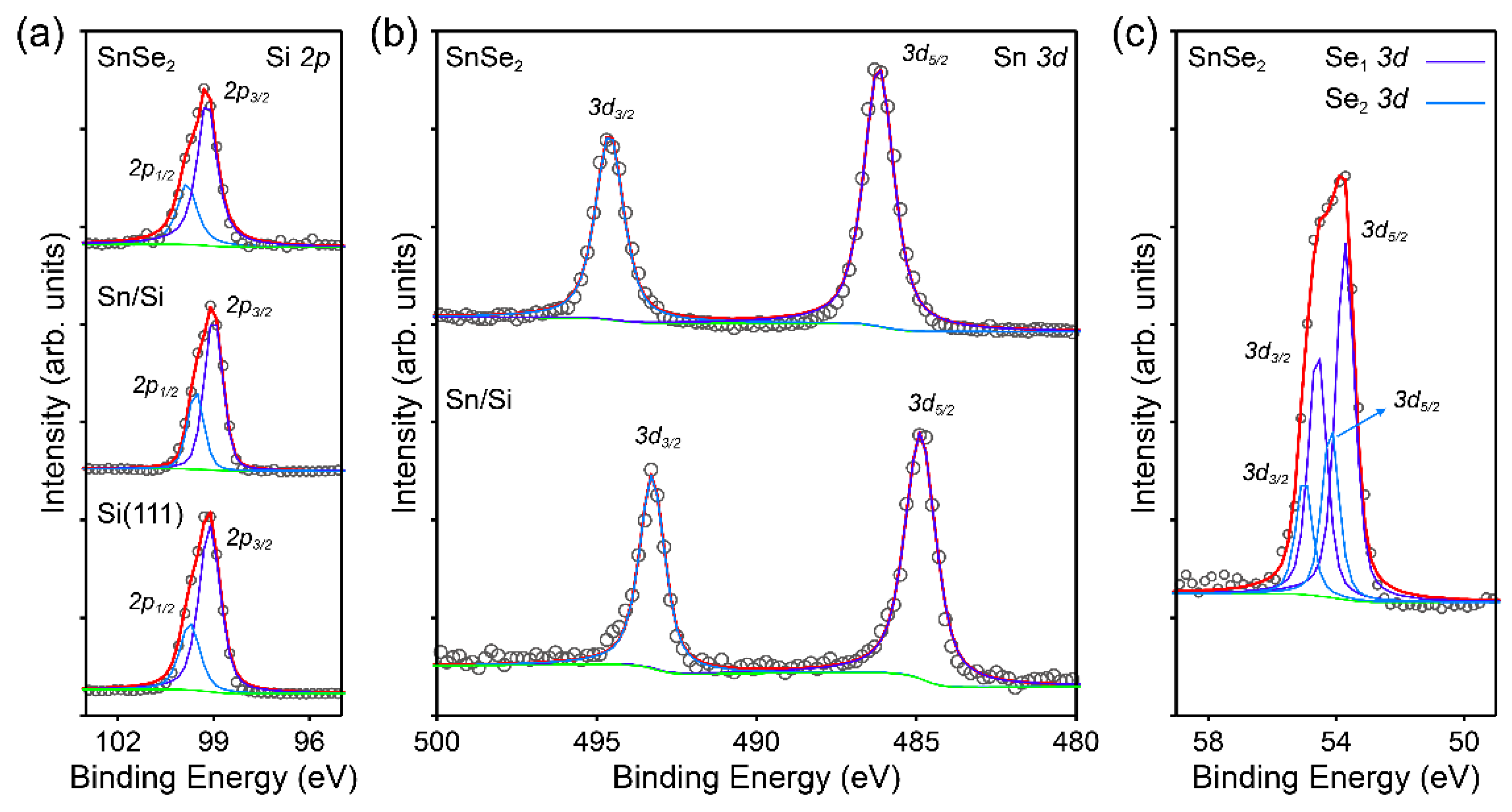
Figure 3.
(a) Schematic illustration of the 2D BZs of Si(111)-(1×1) (blue solid line) and -Sn/Si(111) (red dashed lines) surfaces. (b)&(c) Constant energy mappings taken near the Fermi level of (b) Si(111) and (c) -Sn/Si(111) surface, respectively. The blue and red dashed lines indicate the BZs of Si(111) and -Sn/Si(111). (d) ARPES spectra of Si(111) along the K’-Γ’-M’ direction. (e) Zoom-in ARPES spectra near the Fermi level of -Sn/Si(111) (upper panel) and Si(111) (bottom panel). (f) ARPES spectra of -Sn/Si(111) along the Γ”-M”-Γ”-K”-M” direction.
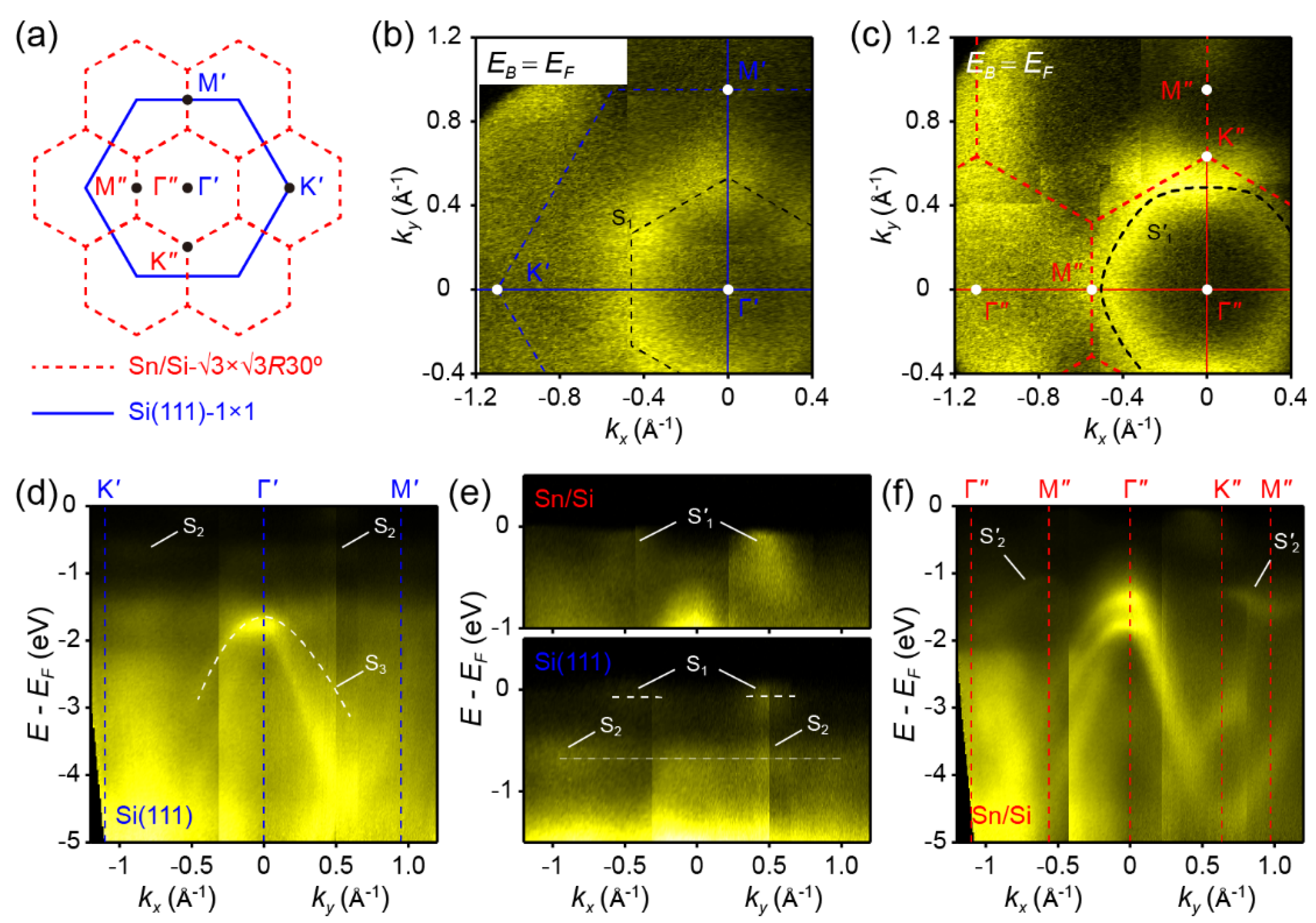
Figure 4.
(a) Constant energy mapping taken near the Fermi level of ML SnSe2. The red dashed lines indicate the 2D BZ of SnSe2. (b-d) ARPES spectra of (b) ML, (c) FL and (d) Multi-L SnSe2 along the Γ-M direction, respectively. (e-g) Zoom-in ARPES spectra near the VBM of (e) ML, (f) FL and (g) Multi-L SnSe2 around the Γ point. (h) EDCs along the red lines in (e-g). The red curves are the Lorentzian fittings to the EDCs. (i-k) Zoom-in ARPES spectra near the CBM of (i) ML, (j) FL and (k) Multi-L SnSe2 around the M point, respectively.
Disclaimer/Publisher’s Note: The statements, opinions and data contained in all publications are solely those of the individual author(s) and contributor(s) and not of MDPI and/or the editor(s). MDPI and/or the editor(s) disclaim responsibility for any injury to people or property resulting from any ideas, methods, instructions or products referred to in the content. |
© 2025 by the authors. Licensee MDPI, Basel, Switzerland. This article is an open access article distributed under the terms and conditions of the Creative Commons Attribution (CC BY) license (http://creativecommons.org/licenses/by/4.0/).
Copyright: This open access article is published under a Creative Commons CC BY 4.0 license, which permit the free download, distribution, and reuse, provided that the author and preprint are cited in any reuse.


