Submitted:
05 May 2025
Posted:
08 May 2025
You are already at the latest version
Abstract
This paper proposes a simple self-oscillating bidirectional buck boost converter circuit design for arbitrary unstable and unpredictable input and output voltage sources. It has built-in abilities to generate switching signals by itself and does not use any integrated circuits. It also can automatically stop itself when over voltage occurs. Both the input and output voltage sources are grounded and isolated from each other.
Keywords:
self-oscillating
; buck-boost converter
; switched mode power supply
1. Introduction
Bidirectional buck boost converters are used in many fields such as electric vehicles, energy systems, mobile electronic devices, etc. [1,2,3,4,5,6,7,8,9,10,11,12,13] It is a kind of switched mode power converter that works by periodically flipping some switches in the circuit on and off. Most switched mode power converter circuit designs in literature are not complete solutions because they do not provide the designs of the additional control circuits needed to generate switching signals, with only a few exceptions [14]. There exists a kind of switched mode power converter that has built-in abilities to generate switching signals and does not use any integrated circuits [15,16,17,18,19,20,21,22,23,24,25,26,27,28,29,30,31]. These circuits are often called self-oscillating converters. The advantages of such circuits are low costs, high reliability, low component count, and not using any integrated circuits. Self-oscillating converters are inherently more suitable for unstable and unpredictable voltage sources because they do not use integrated circuits which typically need a stable power supply to function. As far as this paper knows, there has not been a self-oscillating bidirectional converter in the literature before. This paper will propose a design of a tunable self-oscillating bidirectional buck boost converter circuit to work with arbitrary unstable and unpredictable input and output voltage sources. It will be able to change power flow direction because it is a symmetric design while the power rate will also be adjustable. It has an additional ability to automatically stop if the output voltage has exceeded certain values to protect the voltage sources. Both the input and output voltage sources are connected to the ground. It does not use any integrated circuits and has very low component counts. This circuit can work with direct current voltage sources right away and can also be made to work with alternating current voltage sources by adding rectifiers and inverters. Compared to other self-oscillating converter circuits, the merits of this proposed circuit are that it is bidirectional, has over voltage protection and does not use capacitors so that it will be easier to adjust power rate.
2. Circuit Description
Figure 1 shows the circuits of the proposed bidirectional buck booster converter circuits with intrinsic switching mechanisms. Four slightly different variants are proposed because they will have different characteristics and may suit different situations better. Although they are drawn with bipolar junction transistors later in this paper a simple method will be provided to convert them to use metal–oxide–semiconductor field-effect transistors instead. The principle of the first variant shown in Figure 1 (a) is as follows.
- At the center of the circuit are four coupled inductors which together form a four winding transformer. The inductors L1 and L2 are the main inductors while L3 and L4 are much smaller auxiliary inductors whose purpose is to generate switching signals and the magnetic fields they generated throughout the operations will be insignificant so that they will never affect the operating status of the two main inductors. When the converter circuit is first connected to the direct current voltage source V1, currents will first flow from V1 through resistor R3, R1 and the bipolar junction transistor Q1 to the ground. The current will not flow through L3 and the Zener diode Z3 at this stage because the resistance in this path direction is larger. This will turn Q1 on to be conducting. However, the resistance of R3 is very large so Q1 will be only slightly conducting. This will be enough to turn on L1 and the current across L1 will now rise steadily from zero. The rising magnetic field produced by L1 will then induce an electric potential across L3 so now L3 will act like a voltage source and current will flow from L3 to R1, Q1, Z3 and then back to L3. This current will be much larger than the current flowing through R3 because R3 resistance is super large. So R3 can be ignored at this stage. Because of this current, Q1 will now be fully turned on and fully conducting. And the current through L1 will keep rising until it reaches the saturation point of Q1.
- At this point the current across L1 can no longer increase and as a result the induced electric potential across L3 will drop to zero. This in turn will significantly reduce the current flow from R1 to Q1 to nearly zero. As a result, the saturation point of Q1 is now reduced to nearly zero so that most of the current flowing across L1 cannot flow through Q1 now. In a desperate attempt to maintain the current level at L1, the voltage across L1 will now reverse sign to fall below zero to try to force its current through Q1. But this will also induce a negative electric potential across L3 which will completely deprive R1 of any currents and all the remaining current flowing to R1 will now flow to L3 instead. So now Q1 will be completely shut off and no current from L1 can flow through it. It is at this point that the right half of the circuit will be turned on. Because at this same time, an electric potential will also be induced across L2 which will be just enough to generate a current to flow from ground to V2 via D2 and L2 to maintain the magnetic field level in the transformer core. This current will steadily decrease until it reaches zero. Meanwhile the right half side of this circuit is completely symmetrical to the left half side so by using the same reasonings as previously one can see that Q2 is now fully turned on and ready to conduct currents. When the current flowing through L2 decreases to zero, it will reverse the flow direction and increase again. So now the current will flow from V2 to L2 and then through Q2 to reach the ground until the saturation point of Q2 is reached.
- At this point the right half of the circuit will turn off due to reasons given previously and the left half side of the circuit will turn on again. So, a new cycle will begin. This completes the operating cycle description of this circuit. R1 and R2 are adjustable so the saturation level of Q1 and Q2 are adjustable. Depending on the set saturation levels, the net power flow direction can be made to flow from V1 to V2 or vice versa. Thus, this is a bidirectional converter circuit. Finally, this circuit can prevent overcharging the voltage sources. If the voltage of V2 has increased to beyond the breakdown voltage of Zener diode Z1, then Q5 will turn on which will in turn permanently shut off Q1 until the voltage of V2 drops back below threshold again.
The second circuit variant depicted in Figure 1 (b) replaces L3 and L4 with two additional transistors Q3 and Q4. In the beginning of the operation cycle, R3 will give a small kickstart to Q3 by providing a small current to its base terminal. This will turn on Q1 and L1. After L1 is turned on, a relatively larger current will flow from R5 to Q3 to fully turn on the Q3 and Q1. When the saturation point of Q1 is reached, the voltage across L1 will reverse sign which will deprive the base terminal of Q1 of all currents because now the remaining current will flow from R3 to L1 via D3. The circuit operation will then transition to the right half of the circuit to repeat the above cycles. The saturation point of Q3 during the conducting phase will be large enough to give R1 a reasonable adjust range.
The third circuit variant shown in Figure 1(c) works similarly to the second circuit variant. At first there will be no current through R5 and Q3 because the inductor L1 will prevent the current from changing abruptly. So, then a current will flow from R1 to Q1 to make it fully conducting to allow the current across L1 to increase steadily. During this period Q3 will remain shut off because there will be no electric potential across R5 and Q3. When the saturation point of Q1 is reached, a current will then flow from R5 to Q3 to make it conducible which will cause the current flowing from R1 to Q1 to bypass Q1 and go to Q3 instead.
The fourth variant shown in Figure 1 (d) replaces L1 and L2 with a single inductor L0. It will be slightly different from the previous three variants in that it will be inverting and non-isolating. The operating principle will be similar to that of the second variant except that Q5 will work slightly differently. When V2 drops below the threshold voltage of Z1, the current that was flowing from R3 or R5 to Q3 will go to Q5 instead to deprive Q3 of any currents.
The circuits in Figure 1 use bipolar junction transistors only. However, it will not be difficult to convert those circuits to use metal–oxide–semiconductor field-effect transistors instead. To do so the following structure (Figure 2) can be used to systematically replace the bipolar junction transistors in the circuits in Figure 1. The source terminal of the field effect transistor in the structure will take place of the emitter terminal of the bipolar junction transistor while the drain terminal will take place of the collector terminal and the gate terminal will take place of the base terminal.
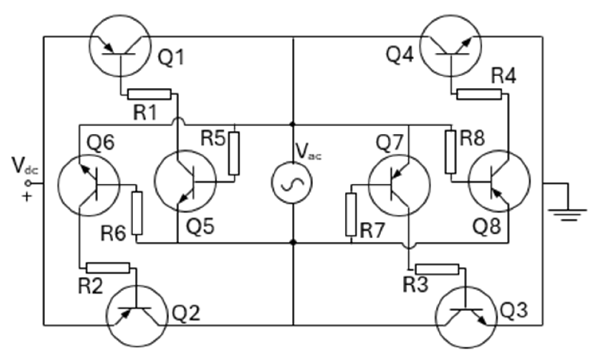
The above power converter circuits will work with dc voltage sources directly. To work with ac voltage sources, rectifiers and inverters will be needed. For alternating current voltage sources with varying and unpredictable frequencies, an inverter that can automatically change its frequency is needed. Figure 3 shows the circuit design of such an automatic inverter. In this circuit, transistor Q5 controls whether Q1 is on or off while Q7 controls Q3 and likewise for the other transistor pairs. When the direction of the ac voltage source Vac is in the up direction, Q5 and Q7 will be turned on while Q2 and Q4 are off so that the main current coming from Vdc will flow from Q1 to Q3. And when Vac is in the downward direction, the current will flow from Q2 to Q4 instead. So, energy will always flow into Vac no matter what its direction is.
3. Circuit Analysis
Finally, the waveforms and other properties of this proposed power converter are analyzed. The waveform of the current flowing into or out of either one of the voltage sources will be a semi sawtooth wave if both input and output voltages are constant. Take V1 for example, at the beginning of the cycle, first a current will flow into V1. Then this current will decrease linearly to zero and then increase linearly in another flow direction. When the current flowing out of V1 increases to a certain value it will suddenly drop to zero and stay zero for a certain period. After that a current will suddenly begin to flow into V1 again to begin a new cycle. The instantaneous power waveform will be of the same shape as the current waveform because the voltages are assumed to be constant here. The waveform shape will also depend on the winding ratios of the transformer in the circuit.
In practice, to achieve optimal efficiency either one of the R1 and R2 should be set to close to infinity depending on which voltage source is the input. In such cases the average power of the converter circuit will increase linearly with the saturation current level of either Q1 or Q2. And the period of the waveform will also increase linearly with the saturation current level. But the waveform will not change linearly with the input or output voltages. If the active phase of input voltage source is much longer than the idle phase, then the average input power will approximately increase with the square of the input voltage while approximately increase linearly with the output voltage and vice versa. So, for general cases the average power will be somewhere between the power of one and two of the voltages.
4. Discussion
The proposed bidirectional buck boost converter circuits can be further simplified if not all functions are needed. For example, Q5 and Z1 can be omitted if there are no over voltage concerns. And most of the right half side of the circuits except D2 and L2 can be omitted if only a unidirectional converter is required. So overall only one transistor is essential to make a functioning buck boost converter. R3 is only used to ensure successful startup of the circuit and may not really be necessary in practice because the idle state is an unstable state and electrical noises in the circuit may already be sufficient to start the circuit.
The proposed four variants of circuits have different advantages. The first variant may be the most efficient but it requires a four winding transformer which in practice may not be easy to obtain. The second variant solves this problem by only needing a standard transformer but has the added complexity of needing more transistors. The third variant uses only a single type of transistor which may be advantageous in practice. The fourth variant only needs a single inductor thus has the greatest flexibility in components but it will no longer be an isolated design. The first three variants are of isolated flyback design. This will make them safe for high voltage applications.
The proposed circuits can be used for a variety of applications. It can be used for electric motors because it can accept unstable and unpredictable output voltages and has regenerative braking abilities. It can be used for low-cost LED lights because of its low-cost design. It can also be used for battery chargers because it can automatically stop itself once the output voltage exceeds certain values.
5. Conclusion
This paper has proposed a kind of self-oscillating buck boost converter that can work with arbitrary unstable and unpredictable voltage sources without using any integrated circuits. An automatic inverter circuit is also provided to work with unpredictable alternating current voltage sources.
Funding
There was no funding.
Data availability
No new data was generated in this paper.
Conflicts of interests
The authors declare no conflicts of interest.
References
- Chiu, Yi-Ching, et al. "Two-Phase Hybrid Buck-Boost Converter With Coupled-Inductors Under ZVS Operation for USB PD Bidirectional Conversion." IEEE Transactions on Circuits and Systems I: Regular Papers (2024).
- Dodda, Satish R, and Srinivasa R. Sandepudi. "Control of three-level bidirectional buck-boost converter for battery energy storage system in bi-polar DC microgrid. Energy Storage 2024, 6, e582. [CrossRef]
- Nimitti, Fabiano Gonzales, and António Manuel Santos Spencer Andrade. "Stacked bidirectional DC-DC converter based on classical boost/buck converter for uninterruptible power supply applications. International Journal of Circuit Theory and Applications 2024, 52, 5338–5356. [CrossRef]
- González-Castaño, Catalina, et al. "A composite DC–DC converter based on the versatile buck–boost topology for electric vehicle applications. Sensors 2022, 22, 5409. [CrossRef]
- Ham, Seok-Hyeong, et al. "High-efficiency Bidirectional Buck–Boost Converter for Residential Energy Storage System. Energies 2019, 12, 3786. [CrossRef]
- Chen, Xi, et al. "Ultra-highly efficient low-power bidirectional cascaded buck-boost converter for portable PV-battery-devices applications. IEEE Transactions on Industry Applications 2019, 55, 3989–4000. [CrossRef]
- Muchina, Eliud G., Lebogang Masike, and Michael Njoroge Gitau. "High boost-ratio bidirectional converter for interfacing low-voltage battery energy storage system to a DC bus. IET Power Electronics 2019, 12, 2372–2381. [CrossRef]
- Satyakar Veeramallu, V. K. , Shunmugam Porpandiselvi, and B. L. Narasimharaju. "Analysis and implementation of soft-switched bidirectional buck-boost DC-DC converter for solar PV-fed LED street lighting systems." International Journal of Circuit Theory & Applications (2019): 47.
- Viswanatha, V. "Microcontroller based bidirectional buck–boost converter for photo-voltaic power plant. " Journal of Electrical Systems and Information Technology 2018, 5, 745–758. [Google Scholar]
- Lee, Hyeon-Seok, and Jae-Jung Yun. "High-efficiency bidirectional buck–boost converter for photovoltaic and energy storage systems in a smart grid. IEEE Transactions on Power Electronics 2018, 34, 4316–4328.
- Wang, Chun, et al. "Efficiency analysis of a bidirectional DC/DC converter in a hybrid energy storage system for plug-in hybrid electric vehicles. Applied energy 2016, 183, 612–622. [CrossRef]
- Elserougi, Ahmed A., et al. "Bidirectional buck-boost inverter-based HVDC transmission system with AC-side contribution blocking capability during DC-side faults. IEEE transactions on power delivery 2014, 29, 1249–1261. [CrossRef]
- Gomis-Bellmunt, Oriol, et al. "Sliding mode control based buck-boost bidirectional converter to drive piezoelectric loads. Electrical Engineering 2007, 90, 115–125. [CrossRef]
- Jung, Hyun Jun, Saman Nezami, and Soobum Lee. "Power supply switch circuit for intermittent energy harvesting. Electronics 2019, 812, 1446.
- Kim, Dongmin, Jongyoon Chae, Ki-Bum Park, and Gun-Woo Moon. "A self-oscillated feedback network for push–pull resonant power converters. IEEE Transactions on Power Electronics 2023, 3811, 14249–14261.
- Rosa, William G., Lucas M. Ilha, Jonas Roberto Tibola, Maikel Fernando Menke, Fábio E. Bisogno, and Álysson R. Seidel. "A control actuation concept for self-oscillating resonant converters. IEEE Journal Of Emerging And Selected Topics In Power Electronics 2021, 103, 3170–3181.
- Zaikin, Denys Igorovych. "Self-oscillating isolated-buck (fly-buck) converter. The Journal of Engineering 2021, 20219, 517–533.
- Lin, Ray-Lee, and Shih-Ho Hsu. "Design and implementation of self-oscillating flyback converter with efficiency enhancement mechanisms. IEEE Transactions on Industrial Electronics 2015, 6211, 6955–6964.
- Chen, Yi, Yurong Nan, Qinggang Kong, and Siheng Zhong. "An input-adaptive self-oscillating boost converter for fault-tolerant LED driving with wide-range ultralow voltage input. IEEE transactions on power electronics 2014, 305, 2743–2752.
- Marvi, Mohammad, Ali Fotowat-Ahmady, Siavash Kananian, and Alireza Zabetian. "A low-distortion self-oscillating power factor correction circuit for low-cost applications. IEEE Transactions on Industrial Electronics 2014, 6111, 6050–6060.
- Suntio, Teuvo. "Average and small-signal modeling of self-oscillating flyback converter with applied switching delay. IEEE transactions on power electronics 2006, 212, 479–486.
- Chen, Feng-Yin, Tsorng-Juu Liang, R-L. Lin, and Jiann-Fuh Chen. "A novel self-oscillating, boost-derived DC-DC converter with load regulation. IEEE transactions on power electronics 2005, 201, 65–74.
- Yang, Yueh-Ru. "A BJT Self-Oscillating Buck-Boost Converter for Battery-Power LED Flashlights." In 2020 IEEE 29th International Symposium on Industrial Electronics (ISIE), pp. 595-600. IEEE, 2020.
- Taeda, Keita, and Hirotaka Koizumi. "A bipolar self-Start up boost converter for thermoelectric energy harvesting." In 2017 IEEE Energy Conversion Congress and Exposition (ECCE), pp. 4747-4752. IEEE, 2017.
- Pedersen, Jeppe A., Mickey P. Madsen, Arnold Knott, and Michael AE Andersen. "Self-oscillating galvanic isolated bidirectional very high frequency dc-dc converter." In 2015 IEEE Applied Power Electronics Conference and Exposition (APEC), pp. 1974-1978. IEEE, 2015.
- Juárez, Mario A., P. R. Martinez, Gerardo Vázquez, José M. Sosa, and Mario Ponce. "Analysis and design for self-oscillating LED driver with high frequency pulsating output current." In IECON 2015-41st Annual Conference of the IEEE Industrial Electronics Society, pp. 003992-003996. IEEE, 2015.
- Venturini, W. A., E. A. Bitencourt, M. E. Schlittler, M. F. da Silva, R. N. do Prado, and F. E. Bisogno. "Analysis and design methodology of a self-oscillating system based on integrated sepic half-bridge for LED lightning applications." In 2013 Brazilian Power Electronics Conference, pp. 1120-1127. IEEE, 2013.
- Sá, E. Mineiro, K. C. A. de Souza, R. P. Coutinho, F. L. M. Antunes, and A. J. Perin. "Self-oscillating buck driver for power LEDs." In 2013 Brazilian Power Electronics Conference, pp. 1128-1133. IEEE, 2013.
- Degrenne, Nicolas, François Buret, Florent Morel, Salah-Eddine Adami, Denis Labrousse, Bruno Allard, and Abderrahime Zaoui. "Self-starting DC: DC boost converter for low-power and low-voltage microbial electric generators." In 2011 IEEE Energy Conversion Congress and Exposition, pp. 889-896. IEEE, 2011.
- de Freitas, LC Gomes, E. A. A. Coelho, J. B. Vieira, V. J. Farias, and L. C. de Freitas. "A new proposal of switched power oscillator applied as a self-oscillating auxiliary medium open loop power supply." In IEEE 34th Annual Conference on Power Electronics Specialist, 2003. PESC'03., vol. 2, pp. 600-605. IEEE, 2003.
- Irving, Brian T., and Milan M. Jovanovic. "Analysis and design of self-oscillating flyback converter." In APEC. Seventeenth Annual IEEE Applied Power Electronics Conference and Exposition (Cat. No. 02CH37335), vol. 2, pp. 897-903. IEEE, 2002.
Figure 1.
The proposed four variants of bidirectional buck boost converter circuit.
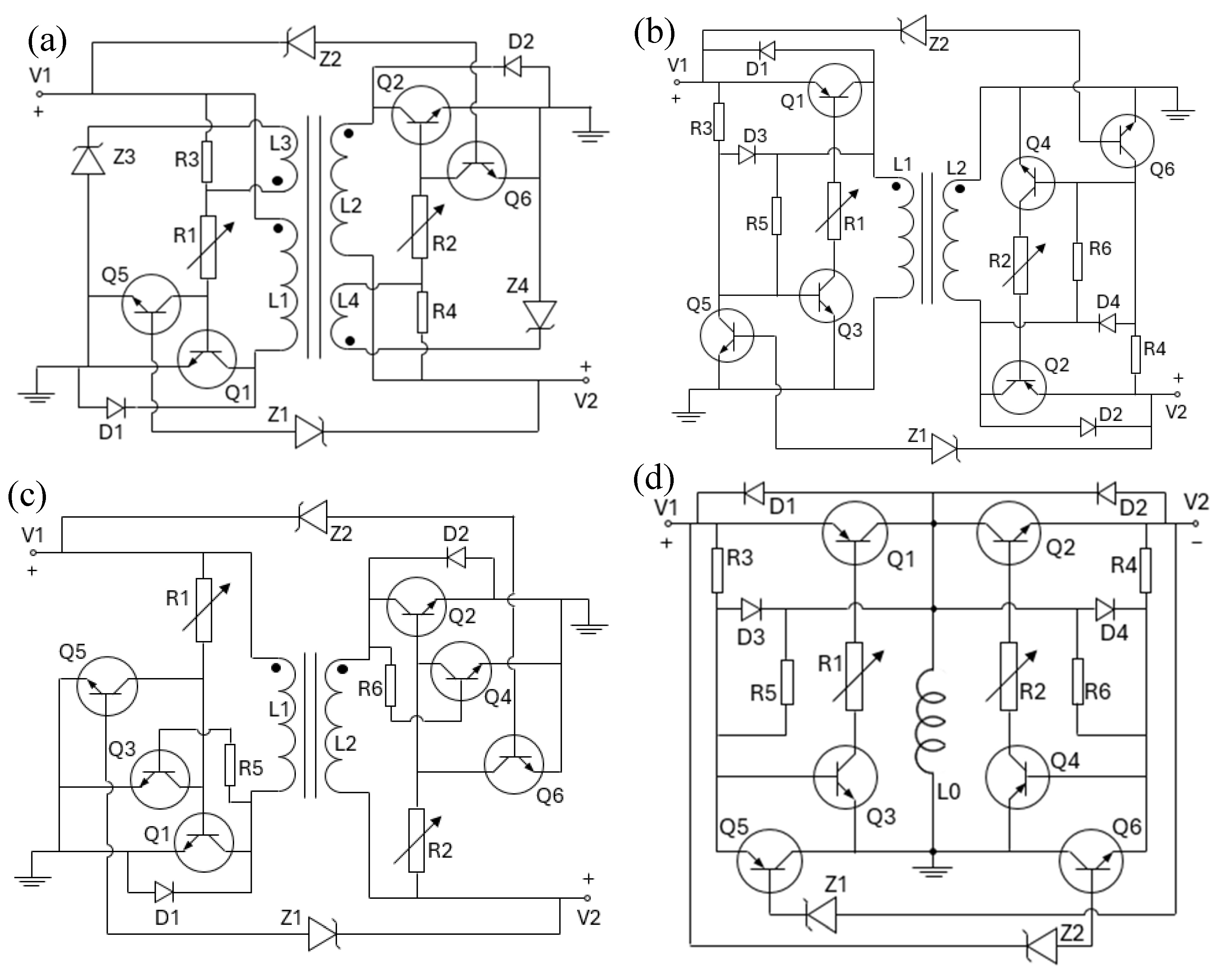
Figure 2.
A structure to systematically replace bipolar junction transistors in the proposed power converter circuits with metal–oxide–semiconductor field-effect transistors.
Figure 2.
A structure to systematically replace bipolar junction transistors in the proposed power converter circuits with metal–oxide–semiconductor field-effect transistors.
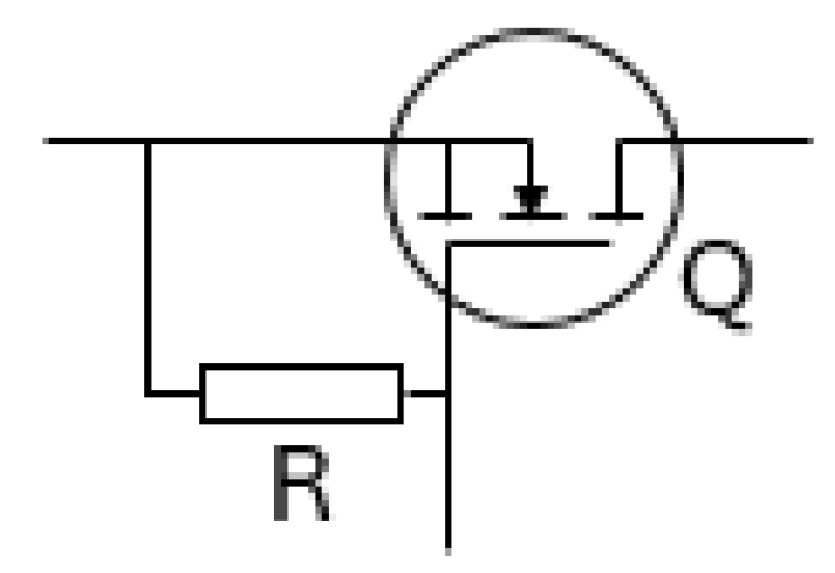
Figure 3.
An automatic inverter to work with ac voltage sources of unpredictable frequencies.
Disclaimer/Publisher’s Note: The statements, opinions and data contained in all publications are solely those of the individual author(s) and contributor(s) and not of MDPI and/or the editor(s). MDPI and/or the editor(s) disclaim responsibility for any injury to people or property resulting from any ideas, methods, instructions or products referred to in the content. |
© 2025 by the authors. Licensee MDPI, Basel, Switzerland. This article is an open access article distributed under the terms and conditions of the Creative Commons Attribution (CC BY) license (http://creativecommons.org/licenses/by/4.0/).
Copyright: This open access article is published under a Creative Commons CC BY 4.0 license, which permit the free download, distribution, and reuse, provided that the author and preprint are cited in any reuse.


