
Submitted:
28 April 2025
Posted:
29 April 2025
You are already at the latest version
Abstract
Gold nanoparticles (AuNPs) were synthesised using ultrasonic spray pyrolysis (USP) with the addition of polyvinylpyrrolidone (PVP) as a stabilising agent and subsequently dried via lyophilisation. The resulting dried AuNPs were redispersed in ethanol, and homogenised to ensure uniform dispersion. This AuNPs` dispersion was then deposited onto a ceramic substrate (Al2O3) using plasma jet printing. Comprehensive characterisation of the dispersion, AuNPs and the resulting printed line were performed using: ICP-OES, SEM/TEM/EDS, UV-Vis, DLS, measurements of dispersion viscosity and printed line roughness. ICP-OES confirmed consistent gold content in the AuNPs` dispersion, while the SEM and EDS analyses revealed predominantly spherical AuNPs with minimal aggregation and similar size distributions. TEM, SAED, and STEM/EDS confirmed the crystalline structure and elemental composition of the AuNPs, with diverse morphologies and strong gold signals. The UV-VIS, DLS, and zeta potential measurements indicated moderate colloidal stability, and TGA verified the AuNPs dispersion’s composition. The AuNPs` dispersion exhibited thixotropic behaviour favourable for printing applications, while confocal microscopy confirmed smooth, uniform printed traces, with an average surface line roughness of 1.65 µm. The successful use of plasma printing with the AuNPs` dispersion highlights its potential for functional material applications in electronics.
Keywords:
Gold nanoparticles
; USP
; dispersion
; plasma jet printing
1. Introduction
The advancement of technology imposes stringent requirements on the materials and fabrication methods used in electronic components [1,2]. Printing techniques capable of creating a wide range of technologically important components have been of great interest recently. Conductive traces and metal electrodes are important parts of all electronic devices, even more so in areas such as space engineering. Satellites operate in harsh environments characterised by extreme temperatures, radiation exposure, and vacuum conditions, necessitating materials that ensure reliability and longevity [3,4]. Printed circuit boards (PCBs), integral to satellite electronics, demand conductive traces that can withstand these challenges [5,6,7]. Traditional fabrication methods and materials often fall short in meeting these demands, prompting the exploration of innovative solutions [8,9,10].
There are various printing techniques, including inkjet, aerosol jet, screen printing and 3D printing, that enable the deposition of metallic materials onto a substrate. However, nanoscale printing of metallic and conducting materials onto a substrate presents significant challenges [11,12,13]. One of the primary problems is ensuring strong adhesion between the printed materials and the substrate, while preserving the substrate`s strength. Traditional printing techniques often require post-processing steps such as thermal annealing or thermal sintering. However, these high temperature treatments can degrade the substrates, compromising their structural integrity. Beyond thermal limitations, achieving uniform and precise deposition on the inherently flexible and uneven surfaces of the substrates remains technically demanding [14]. Nanoscale dispersions must be formulated carefully, to ensure stability, appropriate viscosity and controlled drying characteristics while preventing clogging or inconsistencies during printing. This challenge is particularly pronounced in conventional methods such as inkjet, aerosol jet and screen printing[15].
Plasma jet printing is emerging as an innovative alternative that addresses these challenges more effectively than conventional methods. By utilising a high electric field to eject printing materials and plasma onto substrates precisely, this technique ensures strong adhesion and accurate deposition while preserving the substrates` structural integrity. Plasma jet printing is particularly advantageous for space applications, where traditional printing methods struggle, as it enables high-precision material deposition even under microgravity conditions [16,17,18].
The plasma-jet printer (PJP) is capable of operating in any orientation, including microgravity, because its material flow is driven by electromagnetic forces and the pressure of the carrier gas, rather than gravity [19,20]. It works by atomising nanomaterial ink and using helium gas to transport the resulting mist to the printhead. The printhead itself contains two electrodes positioned around a dielectric ceramic tube, and uses a high-voltage, low-frequency power source to create a dielectric barrier discharge plasma. As the nanomaterials pass through the atmospheric pressure plasma, they can be directed into precise patterns on a target surface. Importantly, the plasma jet also modifies the material properties during printing [21]. The ink is exposed to energetic particles like ions and electrons, which can cause sintering of metallic nanoparticles during deposition. Plasma has been demonstrated to sinter metal nanoparticle films effectively, which offers a major advantage for in-space electronics manufacturing [22]. Unlike other printing methods that require additional heating or light-based annealing after material deposition, plasma-jet printing can perform both deposition and sintering in a single step. This streamlines the process, saving time and resources.
In modern electrical and communication systems, signal integrity is a crucial factor that determines performance and efficiency. However, as signals travel through conductors and transmission lines, they experience various forms of signal loss, which can degrade quality and limit effective transmission. Skin effect is one particularly significant phenomenon at high frequencies, which causes an alternating current (AC) to concentrate near the surface of a conductor rather than utilising its full cross-section. This effect increases the effective resistance of the conductor, leading to additional power dissipation and reduced efficiency. As frequencies rise, the impact of the skin effect becomes more pronounced, making it a critical consideration in RF circuits, high-speed data transmission and power distribution systems. Optimising trace geometry and reducing surface roughness is crucial for minimising the skin effect [23].
In the evolving landscape of printed circuit board (PCB) technology, conductive dispersions have emerged as a game-changing solution for creating electrical traces through innovative printing techniques. Unlike traditional copper etching methods, conductive dispersions enable additive manufacturing, allowing for flexible, lightweight and cost-effective circuit designs. By utilising materials such as silver, copper, carbon and graphene, these dispersions facilitate the development of next-generation electronics, including flexible circuits, wearable devices and rapid PCB prototyping [24,25,26].
Incorporating gold nanoparticles (AuNPs) into conductive dispersions offers significant advantages. Gold is renowned for its excellent electrical conductivity, resistance to oxidation and chemical inertness, making it ideal for reliable conductive traces in PCBs [27,28]. The nanoscale size of AuNPs allows for lower sintering temperatures, enabling their use on temperature-sensitive substrates without compromising performance [29,30,31]. To prepare the dispersion for screen printing, various organic components, including binders, solvents, dispersants and additives, are added to the AuNPs to create a dispersion, which is then used during the printing process [32].
The formulation of AuNPs-based dispersions involves several critical considerations. Stabilising the nanoparticles to prevent aggregation is essential for maintaining uniform dispersion within the product. The rheological properties must be optimised to ensure proper flow during the printing process, achieving the desired resolution and thickness of the printed traces. Additionally, the adhesion of the printed nanoparticles to the substrate is crucial for the mechanical stability of the printed patterns [33,34].
The aim of this research was to develop an AuNPs` dispersion tailored specifically for use with plasma jet printing on solid substrates. The study focuses on formulating a stable and functional dispersion with appropriate physical and chemical properties—such as particle size, viscosity and dispersion stability—that enable effective atomisation and transport within the plasma jet system. Additionally, the research seeks to demonstrate successful deposition of the dispersion onto solid substrates while preserving or enhancing key material properties. The aim is to create a stable, functional AuNPs` dispersion that works well with PJP and can be used to print solid traces on ceramic substrates.
2. Materials and Methods
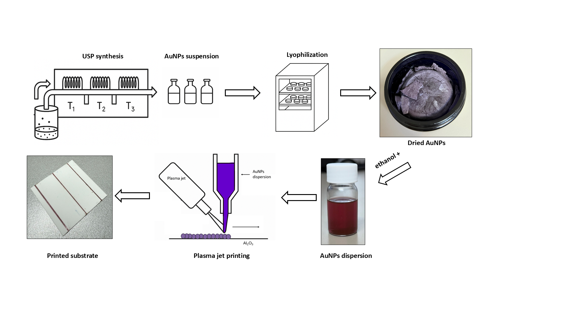
2.1. AuNPs` Synthesis
The AuNPs were synthesised on a proprietary Ultrasonic Spray Pyrolysis (USP) device [35]. The precursor for AuNPs` synthesis was hydrochloric acid HAuCl4 (hydrogen tetrachloroaurate (III) trihydrate; Glentham Life Sciences Ltd, Corsham, UK), dissolved in deionised water, with a concentration of 2 g/l HAuCl4 (an Au content of 50 % gives a concentration of 1 g/l Au). The device uses four custom made ultrasonic generators with 1.6 MHz piezo transducers (Liquifog II, Johnson Matthey Piezo Products GmbH, Germany) for generating aerosol droplets from the precursor solution. The ultrasonic generators are connected to four transport/reaction tubes made from quartz glass, with an internal diameter of 35 mm. Nitrogen gas, N2, was introduced inside the ultrasonic generators, for transporting the aerosol droplets through the tubes at a flow rate of 6 l/min. The tubes are installed inside a reaction tube furnace with three heating zones, with a length of 500 mm for each heating zone. In the first heating zone, aerosol droplet evaporation is carried out at a temperature of 200 °C. A reaction gas, hydrogen, H2, is introduced after the first heating zone at a flow rate of 5 l/min. The two remaining heating zones operate at a temperature of 400 °C each, for reactions of the dried aerosol particles with the hydrogen and the formation of dense AuNPs. The final AuNPs are collected in a gas washing bottle collection system, composed of three consecutively connected gas washing bottles, for each transport/reaction tube. The gas washing bottles contain a collection medium, which is a solution of deionised water with a nanoparticle stabiliser, polyvinylpyrrolidone (PVP, average MW 50,000; Sigma-Aldrich, Germany), with a concentration of 2.5 g/l. The synthesis time for a single batch of AuNPs suspension was 5 hours.
The USP parameters were selected from the results of extensive experimental work conducted on the custom-built, proprietary USP device [35]. The selected parameters yield a favourable AuNPs` suspension synthesis output in terms of quantity, sizes, shapes of AuNPs, with an absence of agglomeration.
The produced AuNPs` suspensions were concentrated by rotary evaporation on a Büchi Rotavapor R-300 (Büchi Labortechnik AG, Flawil, Switzerland). The concentration parameters were: evaporating flask rotation of 200 rpm, bath temperature 40 °C, evaporation pump vacuum 24 mBar. The obtained suspensions were then concentrated further with a PTFE 100,000 MWCO filter membrane (0.1 μm pore size), using a Centurion C2000 centrifuge (Centurion Scientific Limited, Chichester, UK), at 10,000 rpm. The final concentration of AuNPs in the suspension was 5.04 mg/ml Au, analysed with ICP-OES before lyophilisation (freeze-drying).
The lyophilisation was performed on a Labfreez Instruments FD-200F (Labfreez Instruments Group Co., Ltd, Hunan, China). The freezing stage was carried out at -40 °C and ambient pressure for a time of 6 hours. The primary drying (sublimation) was then performed at a temperature of +20 °C and a pressure of 3 Pa for 12 hours. The secondary drying followed, with a set temperature of +30 °C and a pressure of 3 Pa for 30 hours. The total freeze-drying time was 48 hours. The produced dried AuNPs were embedded in a PVP matrix, with a uniform porous structure cake appearance.
2.2. Preparation of the AuNPs` Dispersion
The AuNPs` dispersion for printing was prepared using dried AuNPs stabilised with PVP, which were synthesised and lyophilised in Zlatarna Celje d.o.o. Slovenia.
A volume of 500 mL of ethanol (purity 99.8%, Sigma-Aldrich, Germany) was measured and transferred into a glass beaker. The dried AuNPs were added to the ethanol gradually under continuous stirring. The mixture was stirred at room temperature at 200 rpm using a magnetic stirrer to facilitate the dispersion of the AuNPs. Stirring was continued for 120 minutes to achieve a homogeneous dispersion. Afterwards, the dispersion was poured into a glass flask and sealed to prevent evaporation of the solvent.
Additionally, a dispersion containing 25 ppm of dried AuNPs was prepared in deionised water for particle characterisation (UV-VIS, DLS and zeta potential).
2.3. Plasma jet printing of AuNPs` Dispersion on Al2O3
The conductive lines were printed on a ceramic substrate Al2O3 (96%), with the length and width of 50,8 mm and thickness of 0,635 mm. Figure 1 shows the sketch of our proposed PCB. This sketch outlined the dimensions and structural features required for our experiment and was utilised directly as the template for the plasma jet printing stage.
The first printing was carried out using a FG5001S generator equipped with a PFW10 nozzle (Plasmatreat GmBH, Steinhagen, Germany). The system was operated at a power range of 530–760 W, with nitrogen and air as the process gas, supplied at a flow rate of 33–50 L/min. The nozzle diameter was 5 mm, and the printing speed was maintained between 1 and 2.5 m/min. The precursor flow rate was set between 15 and 30 mL/h, while the carrier gas flow rate ranged from 0 to 15 L/min. The first trial was unsuccessful, because the clogging at the jet head, particularly at the nozzle opening and feeding inlet, was encountered during the process. This problem interrupted the plasma flow and caused irregular material deposition, reducing the overall quality and reproducibility of the printed structures.
As a result, a second trial was carried out, where the AuNPs` dispersion was diluted by ethanol. The second printing was carried out using the same plasma system and jet nozzle as during the first trial. The power was set to 530 W, with a process gas flow rate of nitrogen (N₂) at 33 L/min. The working distance (D) between the nozzle and the substrate was maintained at 5 mm. The deposition speed was controlled at 2.5 m/min. A precursor solution was injected directly into the plasma, with a flow rate of 3 mL/min. The number of deposition cycles was 4. Three traces were printed, with the length of 50 mm and width of 0,55 mm. To ensure the formation of straight lines, the substrate was masked with adhesive tape, covering all areas except for the regions designated for printing.
2.4. Characterisation of the AuNPs` Dispersion and AuNPs
2.4.1. ICP-OES
An ICP-OES analysis was used for the determination of Au concentration in the AuNPs` suspension and dispersion for printing. An HP, Agilent 7500 CE spectrometer, equipped with a collision cell (Santa Clara, CA, USA) was used, with a power of 1.5 kW, a Meinhard nebuliser, a plasma gas flow of 15 L/min, a nebuliser flow of 0.85 L/min, a make-up gas flow of 0.28 L/min, and a reaction gas flow of 4.0 mL/min. The instrument was calibrated with a matrix-matched calibration solution, with a relative measurement uncertainty estimated as ± 3%.
2.4.2. Scanning Electron Microscopy (SEM) and Energy Dispersive X-Ray Spectroscopy (EDS)
The dried AuNPs and prepared ink were analysed with SEM and EDS, using a Sirion 400NC SEM (FEI, Hillsboro, OR, USA), equipped with an INCA 350 EDS (Oxford Instruments, Abingdon, UK). The samples were prepared on standard SEM holder stubs, with a conductive carbon adhesive tape. The prepared AuNPs ink was diluted with ethanol, then put dropwise onto the SEM stub holder with carbon tape and left to dry in a desiccator, while the dried AuNPs were simply transferred to the holder with carbon tape before analysis. The SEM software and ImageJ 1.54 g were used for measuring the nanoparticle sizes. A total of 500 nanoparticles were measured for each sample, for the reproduction of a size distribution chart and descriptive statistics from the measurements.
2.4.3. Transmission Electron Microscopy (TEM) and Energy Dispersive X-Ray Spectroscopy (EDS)
The dried AuNPs embedded in a PVP matrix were mixed with deionised water to dissolve the PVP and release the nanoparticles. The resulting solution was drop-cast onto a TEM grid (lacey formvar carbon film, 300 mesh, Cu) and left to dry in a desiccator overnight before analysis. The sample was examined using imaging, electron diffraction, and elemental composition analysis with a Talos F200i (Thermo Fisher Scientific, Waltham, MA, USA) transmission electron microscope (TEM). The microscope was equipped with a 4k × 4k Ceta™ 16M camera (Thermo Fisher Scientific, Waltham, MA, USA) and an attached Bruker XFlash 6 | 30 energy-dispersive X-ray spectrometer (EDS) (Bruker, Billerica, MA, USA), featuring an energy resolution of 129 eV and a 30 mm² active area chip for a large solid angle. The TEM was operated at an accelerating voltage of 200 kV. The scanning TEM (STEM)/EDS analyses were conducted under standard acquisition conditions.
2.4.4. UV-VIS Spectroscopy
The absorbance spectra were collected using an Infinite 2000 Tecan i-control spectrophotometer using 4.5 mL disposable cuvettes (Fisher Scientific). The absorbance spectra were collected from 350 to 800 nm, with a wavelength step size of 2 nm. AuNPs exhibit distinct surface plasmon resonance (SPR), which is a unique optical property arising from the oscillation of conduction electrons in response to light. A blank sample was measured as well (a cuvette filled with deionised water) so that we could subtract the baseline absorbance due to water, remove background noise or interference from the cuvette or water, as well as ensure that the absorbance measured was due solely to the AuNPs.
2.4.5. Dynamic Light Scattering (DLS) and Zeta Potential
The DLS and zeta potential measurements of the AuNPs` dispersion were made on a Malvern Zetasizer Nano ZS instrument (Malvern Panalytical, Worcestershire, UK). An Omega cuvette Mat. was used, No. 225288. The measurements were carried out at a temperature of 25 °C. The results were analysed with a Litesizer DLS 500 instrument.
2.4.6. Thermogravimetric Analysis (TGA)
The thermogravimetric (TGA) analysis was conducted using a TGA/SDTA, 851, Mettler Toledo analyser, to evaluate the thermal stability and decomposition behaviour of the AuNPs` dispersion. The measurement was conducted under a controlled gas atmosphere. Initially, the sample was heated from 25 °C to 500 °C in a nitrogen (N₂) environment with a gas flow rate of 20 mL/min and a heating rate of 10 K/min. At 500 °C, the gas was switched to oxygen (O₂), and heating was continued up to 800°C under the same flow rate and heating rate. This two-step heating process allowed for the investigation of both thermal degradation in an inert atmosphere and oxidative decomposition.
2.4.7. Rheology Characteristics
Rheological characterisation of the AuNPs` dispersion for printing was performed using a Haake Mars 60 rheometer (Thermo Fisher Scientific). The measurements were carried out using a cone-plate geometry (diameter: 60 mm) at a constant temperature of 25 °C. A 4 mL sample of the dispersion was placed onto the lower plate using a spatula. The upper plate (cone) was then lowered onto the sample, establishing a fixed gap of 0.15 mm between the plates.
A shear protocol was applied, to investigate the sample's structural response and recovery behaviour. The sample was first sheared at 1 s⁻¹ for 400 seconds, followed by a high shear rate of 200 s⁻¹ for 100 seconds. The shear rate was then reduced back to 1 s⁻¹, to monitor the potential structural reformation within the AuNPs` dispersion.
2.4.8. Surface Roughness of the Printed Line
To evaluate the suitability of plasma jet printing on solid substrates, the surface roughness of the AuNPs printed line was analysed using a confocal optical microscope, Axio CSM 700 (Zeiss, Jena, Germany) in accordance with the ISO 25178 Standards for areal surface texture. The measurements were performed using a 1500 × total magnification, capturing an effective scan of approximately 117 µm x 93 µm. The primary roughness parameter extracted was the arithmetic mean height (Sa), which offers a 3D areal analogue to average roughness (Ra), and is better suited for assessing the texture of functional surfaces with complex morphology. The surface roughness of the AuNPs printed line was measured at three distinct locations on the printed trace, to ensure the reproducibility and statistical reliability of the results.
2.4.9. Statistical Analysis
The descriptive statistics and data analysis were conducted using Microsoft Excel (Microsoft Corp., Redmond, WA, USA), utilising its built-in functions.
3. Results
3.1. ICP-OES
The results of the Au concentration in the AuNPs` dispersion after USP and for printing are presented in Table 1.
3.2. SEM and EDS Analyses Results of AuNPs
The dried AuNPs and the prepared AuNPs` dispersion were characterised with SEM and EDS for a direct comparison of the AuNPs shapes, sizes and agglomeration state in these different dispersion formulations. Figure 2 shows the AuNPs analysed from the dried PVP cake and from the prepared dispersion. The shapes of the AuNPs were mostly spherical, with some irregularly shaped particles. The smaller AuNPs below 100 nm were predominantly spherical, while the irregular shapes were more present with larger AuNPs. The smallest measured AuNPs were around 10 nm in diameter, while the largest recorded were around 300 nm. The AuNPs were present as individual particles or in clusters, which may be the result of the presence of the PVP stabiliser, grouping the individual particles together during preparation of the samples for SEM. Upon closer examination, the clusters contained single discrete particles, and aggregation or agglomeration was usually not present.
The EDS analysis showed a high value of carbon – C, because of the sample holder, as the samples were prepared on a SEM stub holder with carbon tape, as well as due to the presence of the stabiliser PVP. Oxygen – O may also be attributed to the presence of the stabiliser PVP. Au was obtained in both sample types, confirming the AuNPs content. The presence of the PVP stabiliser also hinders the SEM image acquisition of the samples somewhat, as it is a non-conductive compound which was blurring the edges of the AuNPs in the obtained SEM images.
Figure 2 includes size distribution charts for the sample types with a bin width of 10 nm. The size measurements showed similar values for the dried AuNPs and for AuNPs in the prepared dispersion, with comparable minimum and maximum sizes of the AuNPs (7.3 and 7.7 nm for the minimum values with 310.9 and 357.5 nm for the maximum values, for the dried AuNPs and AuNPs` dispersion respectively). The mean values were also quite close (71.5 for the dried AuNPs and 69.5 nm for the AuNPs` dispersion), while the standard distribution was greater in the prepared dispersion (35.6 for the dried AuNPs and 53.1 nm for the AuNPs` dispersion). The size distribution charts also showed a broader size range for the prepared dispersion. This may be attributed to some aggregation of the smallest AuNPs because of the dispersion preparation and later dilution of this dispersion with ethanol, for preparation of the sample for SEM and EDS analysis. Additionally, the measurement sample of 500 particles may have some effect on the differences of the obtained size distributions.
The comparison of nanoparticles in the dried AuNPs and the prepared AuNP dispersion showed minimal differences in the particle characteristics. Some aggregation of the particles was present in the prepared AuNP dispersion, as compared to the dried AuNPs.
3.3. TEM and STEM/EDS Analyses Results of AuNPs
Figure 3 presents the TEM, selected area electron diffraction (SAED), and STEM/EDS results of the synthesised dried AuNPs. Figure 3a,c display AuNPs at low and high magnifications, revealing variations in size and shape. At lower magnification, some agglomeration is visible. The particle sizes range from 5 nm to 150 nm. The smallest AuNPs (~5–10 nm) are predominantly spherical, whereas the larger particles exhibit mainly rectangular shapes, with some also appearing hexagonal or triangular.
Figure 3b shows the SAED pattern, where diffraction rings and brighter spots—corresponding to larger particles—confirm the crystalline nature of the AuNPs. The diffraction spots align with the Au reflections (PDF No. 00-004-0784), as marked in the image.
Figure 3c provides a higher-resolution view, offering better insight into the morphology of the smaller AuNPs. Twinning effects, associated with particle growth, are also observed. The inset presents the 2D Fast Fourier Transform (FFT), with diffraction spots corresponding to the (111) plane.
Figure 3d illustrates the STEM/EDS analysis of the AuNPs. The inset shows strong EDS signals at Lα1 = 9.711 keV and Lα2 = 9.628 keV, confirming the presence of gold (highlighted in green in the mapping image). The peaks corresponding to carbon, nitrogen, oxygen, and silicon originated mainly from the TEM grid film and residual synthesis solvents. The unmarked peaks at Kα = 8.04 keV and Kβ = 8.91 keV are attributed to the TEM grid material.
3.4. UV-VIS
The blue curve in Figure 4 represents the baseline absorbance of the deionised water, the green curve represents the absorbance of AuNPs in the deionised water, and the orange curve represents the difference between the blue and green curves, subtracting the blank values from the AuNPs` suspension to isolate the contribution of the nanoparticles to the overall absorbance. The characteristic peak of AuNPs is generally observed between 500 and 600 nm, due to the surface plasmon resonance effect [36]. A distinct peak in the 500-600 nm range can be observed on both the green and orange curves, indicating a successful formation of AuNPs. A comparison with the blue curve (blank) confirms the specific optical contribution of the nanoparticles.
3.4. DLS
The purpose of the DLS analysis was to investigate the hydrodynamic diameter of the AuNPs and the polydispersity of the dispersion. Figure 5 shows the curve which represents the hydrodynamic diameter of AuNPs in deionised water. The average hydrodynamic diameter is 180 nm, with a polydispersity of 25 % and a Standard Deviation of 2.93 nm. The statistical analysis of the DLS measurement is presented in Table 2. The average particle diameters obtained from the DLS were consistently larger than those observed by TEM. This discrepancy arises because DLS measures the hydrodynamic diameter, which includes not only the solid particle core, but also any surface coatings, bound solvent layers, and dynamic interactions with the surrounding medium. In contrast, TEM provides a direct visualisation of the particle core under dry conditions, excluding these additional contributions. Furthermore, DLS yields an intensity-weighted size distribution, making it particularly sensitive to the presence of larger particles or aggregates, whereas TEM analysis typically results in a number-weighted distribution. These methodological differences explain the larger apparent sizes observed in the DLS measurements.
3.5. Zeta Potential
The results of the zeta potential for the AuNPs` dispersion in deionised water are presented in Figure 6. The curve shows a peak at -12.4 mV. This relatively low negative value suggests moderate colloidal stability, indicating that electrostatic repulsion alone is insufficient to provide strong stabilisation. This can be attributed to the presence of PVP, which acts primarily as a steric stabiliser rather than an electrostatic one – PVP stabilises the AuNPs by forming a protective polymeric layer around them, preventing agglomeration through steric hindrance rather than charge repulsion [37].
3.6. TGA
Figure 7 shows the TGA curve of the AuNPs` dispersion, where its change of relative weight is visible as the temperature increases. The TGA curve shows an initial rapid mass loss up to approximately 120 °C (region A), due primarily to the evaporation of ethanol and any residual water present in the sample. This phase accounts for the most significant weight reduction. Between 150 and 400 °C, the mass loss occurs gradually, indicating the thermal decomposition of PVP. The degradation of the polymer stabiliser begins progressively around 250–350 °C. As the temperature increases to approximately 400–500 °C, a more pronounced mass loss is observed, corresponding to the complete decomposition of PVP and any remaining organic residues (region B) [38]. Above 500 °C, the mass stabilises, representing the inorganic content of the sample, primarily AuNPs, which remain intact at these temperatures.
3.7. Rheology Measurement
Figure 8 illustrates the thixotropic behaviour of the AuNPs` dispersion, showing the evolution of viscosity as a function of time. The viscosity remains relatively constant during the initial stage, with only minor fluctuations, indicating the structural stability of the paste at rest. This is typical for thixotropic materials, where internal particle interactions maintain a stable network structure under quiescent conditions. At approximately 500 seconds, a noticeable decrease in viscosity is observed, corresponding to the application of an increased shear rate. This reduction is characteristic of thixotropic behaviour, where the internal structure of the material breaks down under shear, resulting in a lower viscosity [39]. Following the decrease in shear rate at around 600 seconds, the viscosity increases gradually and approaches its initial value. This recovery suggests reformation of the internal particle network and partial restoration of the original microstructure. Subsequently, the viscosity stabilises again, indicating that the dispersion reaches a new equilibrium state.
3.8. Analysis of the Printed Lines
The initial trials of plasma jet printing, as shown in Figure 6a–c, did not yield successful or uniform coatings under the tested process conditions. Visible in the images, the deposition appears inconsistent, with significant irregularities and non-uniform coverage across the substrate surfaces. This was observed regardless of the combinations of process gas (air or N₂) and carrier gas (air or N₂). Such outcomes suggest that the process parameters (e.g., gas composition, flow rates, substrate temperature, plasma power), were not optimised for stable or effective material deposition. In particular, the evident streaks, patchiness, white colour and incomplete coverage, indicate insufficient interaction between the plasma jet and the precursor material. A major challenge encountered during these experiments was the clogging and agglomeration of PVP within the nozzle head. This was compounded by coagulation of the dispersion at the precursor inlet, both of which hindered consistent precursor delivery to the plasma jet. These issues likely contributed to the observed non-uniform film formation and interrupted deposition process.
Figure 10 b) shows the printed substrate after the second plasma printing trial, where three distinct lines can be observed. Each line is 50 mm in length, 0,55 mm in width and 0,008 mm in thickness. Figure 10 a) shows the magnified bottom line. Figure 10 c) shows the SEM image of the line. The presence of the purple colour confirms the successful incorporation of AuNPs along the printed line (Fig. 10 a). This indicates that there was no segregation, agglomeration, or formation of bulk gold—which would have been observed as a golden colour—thus confirming the nanostructured character of the deposited gold. A detailed examination of the printed line revealed that the edges were not straight, which poses a problem (the lateral roughness was too high compared to the requirements specified in Figure 1). Based on this, it will be necessary in future printing processes to design a mask that enables compliance with the tolerance requirements for edge straightness and lateral roughness, as required for these applications. This mask will also ensure that there is no outflow of dispersion during deposition on Al₂O₃. An EDS analysis was carried out to verify the elemental composition of the printed lines (Table 3). The EDS spectra revealed significant variations in elemental composition depending on the region analysed. Spectrum 1 and Spectrum 6 exhibited elevated carbon content, which is attributed primarily to the carbon sample holder used during the measurement. The presence of aluminium in these spectra, as well as the associated oxygen signal, is consistent with the Al₂O₃ substrate. Additionally, oxygen may also be attributed partially to the presence of the PVP used in the preparation process. Gold was detected in spectra 2–5, corresponding to areas where the AuNPs were printed on the substrate, confirming successful deposition.
Figure 11 shows the height profile (left), a 3D topographic image of the surface (middle) and the Sa values (right). The Sa values across all three scan regions ranged from 1.28 to 2.12 µm, with an average Sa of 1,65 µm. These values confirm that the printed AuNPs traces exhibit a sufficiently smooth surface topography. The absence of sharp peaks or significant waviness further suggests that the plasma printing process yields a stable and uniform film formation.
4. Discussion
The ICP-OES analysis provided quantitative data on the concentration of gold in both the dried AuNPs obtained after USP and the final dispersion for printing. This allowed accurate monitoring of the gold content throughout the synthesis and redispersion processes, ensuring consistent nanoparticle yield and enabling comparison between different sample states.
The comparative SEM and EDS analyses of dried AuNPs and the prepared AuNPs` dispersion provided valuable insights into the nanoparticle morphology, size distribution, and dispersion stability. In both sample types, the AuNPs were primarily spherical, with irregular shapes observed more commonly among the larger particles. This morphological similarity suggests that the synthesis and stabilisation process is robust and produces uniform nanoparticles consistently.
Both the dried and dispersed AuNPs displayed similar size distributions, with comparable minimum and maximum diameters and closely matching mean sizes. However, the broader size distribution in the dispersion, reflected by a higher Standard Deviation, may indicate minor aggregation during the redispersion and ethanol dilution steps. This suggests that, while PVP stabilises the nanoparticles effectively, some degree of size variation is introduced during sample handling.
The EDS confirmed the presence of elemental gold in both sample types, while the high carbon and oxygen signals were attributed to the use of carbon tape and the PVP stabiliser. The non-conductive nature of PVP also affected the SEM imaging quality slightly by obscuring the nanoparticle edges, potentially impacting the agglomeration assessments.
The TEM, SAED, and STEM/EDS analyses confirmed the structural and elemental integrity of the synthesised AuNPs further. The TEM revealed a broad range of sizes (5–150 nm) and morphologies, including spherical, triangular and polygonal shapes. The SAED and FFT confirmed the crystalline nature of the particles, particularly the presence of the (111) crystallographic plane. The EDS mapping supported the elemental composition, showing strong gold signals, with additional peaks corresponding to residual synthesis materials and the TEM grid.
The UV-VIS spectroscopy confirmed the successful formation of AuNPs, as evidenced by the surface plasmon resonance peak between 500 and 600 nm. The DLS analysis indicated a moderate polydispersity and a hydrodynamic diameter of around 180 nm. The zeta potential of –12.4 mV reflects the steric stabilisation effect of PVP, which supports colloidal stability to a moderate degree.
The TGA analysis identified ethanol, PVP, and gold as the major components of the dispersion. The final residual mass confirmed the gold content after the decomposition of organic materials, offering insight into the formulation's stability and composition.
The rheological evaluation revealed thixotropic behaviour in the dispersion, suggesting reversible structural breakdown and recovery under shear. This is beneficial for applications requiring good flowability and shape retention, such as printing technologies.
The formulated AuNPs` dispersion demonstrated appropriate rheological and colloidal stability characteristics for use in plasma jet printing. This was evidenced by the successful deposition of three uniform lines, each approximately 5 cm in length, on Al2O3. The printed patterns exhibited good continuity and adhesion, indicating that the dispersion was well-suited for this additive manufacturing approach. Surface characterisation using confocal optical microscopy demonstrated low surface roughness and consistent deposition, with Sa values ranging from 1.28 µm to 2.12 µm. This indicates smooth and uniform film formation on ceramic substrates.
However, achieving an ultra-thin layer of approximately 8 µm presents challenges for SEM/EDX characterisation, which, typically, has a penetration depth of up to 6 µm. This limitation may result in incomplete analysis of the layer’s composition. Additionally, the presence of stabilisers containing elements such as oxygen and carbon can interfere with accurate elemental analysis. The EDS analysis (Table 3) revealed the presence of these stabilisers, suggesting the need for post-deposition thermal treatment to remove them.
The achieved low surface roughness (< 2.8 μm) is particularly beneficial for high-frequency signal transmission (20–60 GHz), where the skin effect becomes significant [40,41]. A smooth surface minimises signal loss, which is crucial for the performance of printed electronic devices. The presence of stabilisers, while necessary for dispersion stability, must be managed carefully, as residual stabilisers can affect the electrical properties of the printed layers adversely. Thermal treatment has proven effective in reducing the stabiliser content, thereby enhancing conductivity.
The prepared AuNPs` dispersion has the potential to be used as a specialised conductive ink, especially for radio frequency applications [42]. One of the main benefits of plasma jet printing is that it allows the direct use of dispersions without the need for extensive rheological optimisation, which is typically required for screen-printable or stencil-printable inks. In conventional processes, the inks must be engineered to meet strict viscosity and thixotropy criteria [43]. In contrast, plasma jet printing is a contactless, direct-write method, that is far less dependent on the rheological properties of the ink or dispersion [44]. If the colloidal stability and particle size are appropriate for the nozzle and process, even low-viscosity dispersions can be printed effectively. This flexibility means that the synthesised AuNPs` dispersion—without additional thickening agents —can be used directly in plasma jet printing. Our study also suggests that utilising the dispersion directly after USP synthesis could reduce the stabiliser content significantly, potentially by up to five times. This approach may simplify the processing steps.
Overall, the combined characterisation confirms that the synthesised AuNPs possess desirable structural, chemical and colloidal properties. Moreover, the successful application of plasma printing with the AuNPs` dispersion demonstrates the practical potential of this formulation for advanced functional material printing. Future work will focus on evaluating electrical properties, such as conductivity, impedance, and the skin effect for electronic device integration.
5. Conclusions
Based on our research findings, we draw the following conclusions:
- The synthesised AuNPs` dispersion is suitable for plasma jet printing, enabling the successful deposition of AuNPs lines on Al₂O₃ with an achieved thickness of approximately 8 μm.
- The printed lines are purple in colour, confirming the presence of AuNPs; however, PVP remains present on the lines.
- The surface roughness of the printed lines ranged from 1.28 μm to 2.12 μm, thereby meeting the requirement for RF applications (< 2.8 μm). This result demonstrates the potential for further development. The smoothness achieved is advantageous for applications in PCBs, particularly in high-frequency signal transmission where surface quality is crucial.
Author Contributions
Conceptualisation, R.R. and L.K.; methodology, L.K., P.M. and R.R.; software, P.M.; validation, R.R.; formal analysis, L.K. and D.F.; investigation, L.K., P.M., D.F. and R.R.; resources, R.R.; data curation, P.M.; writing—original draft preparation, L.K. and P.M.; writing—review and editing, P.M., D.F. and R.R.; visualisation, L.K. and P.M; supervision, R.R.; project administration, R.R.; funding acquisition, R.R. All the authors have read and agreed to the published version of the manuscript.
Funding
This research and APC was funded by the Slovenian Research Agency ARIS: P2-0120 Research program, Young Researcher No. 1000-2025-0552 and International Infrastructure Project EuBi (I0-E014).
Data Availability Statement
The raw data supporting the conclusions of this article will be made available on request.
Conflicts of Interest
The authors Peter Majerič and Rebeka Rudolf were employed by the company Zlatarna Celje d.o.o. The remaining authors declare that the research was conducted in the absence of any commercial or financial relationships that could be constructed as a potential conflict of interest.
Abbreviations
AuNPs – gold nanoparticles, Al2O3 – aluminum oxide, DLS – dynamic light scattering, EDS – energy dispersive X-ray spectroscopy, ICP-OES – inductively coupled plasma optical emission spectroscopy, PVP – polyvinylpyrrolidone, SAED – selected area electron diffraction, SEM – scanning electron microscopy, TEM – transmission electron microscopy, TGA – thermogravimetric analysis, USP – ultrasonic spray pyrolysis, UV-Vis – ultraviolet-visible spectroscopy
References
- Norman, S. Das, T. Rohr, T. Ghidini, Advanced manufacturing for space applications, CEAS Space Journal 15 (2023) 1–6. [CrossRef]
- A.V. Bounegru, C. Apetrei, Carbonaceous nanomaterials employed in the development of electrochemical sensors based on screen-printing technique—a review, Catalysts 10 (2020). [CrossRef]
- A. Kamyshny, S. Magdassi, Conductive nanomaterials for printed electronics, Small 10 (2014) 3515–3535. [CrossRef]
- H.W. Tan, Y.Y.C. Choong, C.N. Kuo, H.Y. Low, C.K. Chua, 3D printed electronics: Processes, materials and future trends, Prog Mater Sci 127 (2022). [CrossRef]
- J. Lemarchand, N. Bridonneau, N. Battaglini, F. Carn, G. Mattana, B. Piro, S. Zrig, V. Noël, Challenges, Prospects, and Emerging Applications of Inkjet-Printed Electronics: A Chemist’s Point of View, Angewandte Chemie - International Edition 61 (2022). [CrossRef]
- B.F.Y. Rezaga, M.D.L. Balela, Chemical sintering of Ag nanoparticle conductive inks at room temperature for printable electronics, Journal of Materials Science: Materials in Electronics 32 (2021) 17764–17779. [CrossRef]
- I.J. Fernandes, A.F. Aroche, A. Schuck, P. Lamberty, C.R. Peter, W. Hasenkamp, T.L.A.C. Rocha, Silver nanoparticle conductive inks: synthesis, characterization, and fabrication of inkjet-printed flexible electrodes, Sci Rep 10 (2020). [CrossRef]
- H. Li, X. Zhu, Z. Li, J. Yang, H. Lan, Preparation of nano silver paste and applications in transparent electrodes via electric-field driven micro-scale 3D printing, Nanomaterials 10 (2020). [CrossRef]
- M. Wang, X. Xu, B. Ma, Y. Pei, C. Ai, L. Yuan, Fabrication of micron-SiO2@nano-Ag based conductive line patterns through silk-screen printing, RSC Adv 4 (2014) 47781–47787. [CrossRef]
- R.M. Silva, A.D. da Silva, J.R. Camargo, B.S. de Castro, L.M. Meireles, P.S. Silva, B.C. Janegitz, T.A. Silva, Carbon Nanomaterials-Based Screen-Printed Electrodes for Sensing Applications, Biosensors (Basel) 13 (2023). [CrossRef]
- K. Yan, J. Li, L. Pan, Y. Shi, Inkjet printing for flexible and wearable electronics, APL Mater 8 (2020). [CrossRef]
- C.H. Rao, K. Avinash, B.K.S.V.L. Varaprasad, S. Goel, A Review on Printed Electronics with Digital 3D Printing: Fabrication Techniques, Materials, Challenges and Future Opportunities, J Electron Mater 51 (2022) 2747–2765. [CrossRef]
- K. Hassan, M.J. Nine, T.T. Tung, N. Stanley, P.L. Yap, H. Rastin, L. Yu, D. Losic, Functional inks and extrusion-based 3D printing of 2D materials: A review of current research and applications, Nanoscale 12 (2020) 19007–19042. [CrossRef]
- Y.Z.N. Htwe, M. Mariatti, Printed graphene and hybrid conductive inks for flexible, stretchable, and wearable electronics: Progress, opportunities, and challenges, Journal of Science: Advanced Materials and Devices 7 (2022). [CrossRef]
- M. Jafarpour, F. Nüesch, J. Heier, S. Abdolhosseinzadeh, Functional Ink Formulation for Printing and Coating of Graphene and Other 2D Materials: Challenges and Solutions, Small Science 2 (2022). [CrossRef]
- R.P. Gandhiraman, V. Jayan, J.W. Han, B. Chen, J.E. Koehne, M. Meyyappan, Plasma jet printing of electronic materials on flexible and nonconformal objects, ACS Appl Mater Interfaces 6 (2014) 20860–20867. [CrossRef]
- P. Doshi, Z. Li, F. Langer, D.H. Gutierrez, N. Benson, D. Nordlund, D.G. Senesky, R.P. Gandhiraman, Plasma Jet Printing of Diamond and Silicon, IEEE Journal on Flexible Electronics 3 (2024) 252–258. [CrossRef]
- Hagger, M.A. Parkes, F. Lockwood Estrin, S. Agrotis, I.P. Parkin, A.D. Handoko, D.J. Caruana, Additive metal printing on multi materials using an atmospheric pressure plasma jet on a 5-Axis platform, Mater Des 251 (2025). [CrossRef]
- R.P. Gandhiraman, E. Singh, D.C. Diaz-Cartagena, D. Nordlund, J. Koehne, M. Meyyappan, Plasma jet printing for flexible substrates, Appl Phys Lett 108 (2016). [CrossRef]
- R. Ramamurti, R.P. Gandhiraman, A. Lopez, P. Doshi, D. Nordlund, B. Kim, M. Meyyappan, Atmospheric pressure plasma printing of nanomaterials for IoT applications, IEEE Open Journal of Nanotechnology 1 (2020) 47–56. [CrossRef]
- J. Manzi, A.E. Weltner, T. Varghese, N. McKibben, M. Busuladzic-Begic, D. Estrada, H. Subbaraman, Plasma-jet printing of colloidal thermoelectric Bi2Te3 nanoflakes for flexible energy harvesting, Nanoscale 15 (2023) 6596–6606. [CrossRef]
- Reinhold, C.E. Hendriks, R. Eckardt, J.M. Kranenburg, J. Perelaer, R.R. Baumann, U.S. Schubert, Argon plasma sintering of inkjet printed silver tracks on polymer substrates, J Mater Chem 19 (2009) 3384–3388. [CrossRef]
- J. Coonrod, Insertion Loss Comparisons of Common High Frequency PCB Constructions, n.d.
- S. Ghadimi, S. Mazinani, A.M. Bazargan, F. Sharif, Effect of formulation and process on morphology and electrical conductivity of Ag-graphene hybrid inks, Synth Met 281 (2021). [CrossRef]
- W. Li, Q. Sun, L. Li, J. Jiu, X.Y. Liu, M. Kanehara, T. Minari, K. Suganuma, The rise of conductive copper inks: challenges and perspectives, Appl Mater Today 18 (2020). [CrossRef]
- K. Parvez, R. Worsley, A. Alieva, A. Felten, C. Casiraghi, Water-based and inkjet printable inks made by electrochemically exfoliated graphene, Carbon N Y 149 (2019) 213–221. [CrossRef]
- P.T. Bishop, L.J. Ashfield, A. Berzins, A. Boardman, V. Buche, J. Cookson, R.J. Gordon, C. Salcianu, P.A. Sutton, Printed gold for electronic applications, 2010. www.goldbulletin.org.
- Hammami, N.M. Alabdallah, A. Al jomaa, M. kamoun, Gold nanoparticles: Synthesis properties and applications, J King Saud Univ Sci 33 (2021). [CrossRef]
- H.R. Tiyyagura, P. Majerič, M. Bračič, I. Anžel, R. Rudolf, Gold inks for inkjet printing on photo paper: Complementary characterisation, Nanomaterials 11 (2021) 1–13. [CrossRef]
- T. Valayil Varghese, J. Eixenberger, F. Rajabi-Kouchi, M. Lazouskaya, C. Francis, H. Burgoyne, K. Wada, H. Subbaraman, D. Estrada, Multijet Gold Nanoparticle Inks for Additive Manufacturing of Printed and Wearable Electronics, ACS Materials Au 4 (2024) 65–73. [CrossRef]
- Reiser, L. González-García, I. Kanelidis, J.H.M. Maurer, T. Kraus, Gold nanorods with conjugated polymer ligands: Sintering-free conductive inks for printed electronics, Chem Sci 7 (2016) 4190–4196. [CrossRef]
- Y. Qin, X. Ouyang, Y. Lv, W. Liu, Q. Liu, S. Wang, A Review of Carbon-Based Conductive Inks and Their Printing Technologies for Integrated Circuits, Coatings 13 (2023). [CrossRef]
- Le Porcher, M. Rieu, J.P. Viricelle, Development of Gold Inks for Inkjet Printing of Gas Sensors Electrodes on Plastic Support, Electronics (Switzerland) 13 (2024). [CrossRef]
- Juric, H. Hao, E. Ermantraut, K. Glaser, W. Eberhardt, A. Zimmermann, Laser Irradiation for Improving the Wetting of Nanoparticle Gold Inks for Printed Electronics, IEEE Trans Compon Packaging Manuf Technol 10 (2020) 325–331. [CrossRef]
- Rudolf R, Majerič P, Štager V, Albreht B, Process for the production of gold nanoparticles by modified ultrasonic spray pyrolysis: patent application no. P-202000079, P-202000079, 2020.
- N. Sarfraz, I. Khan, Plasmonic Gold Nanoparticles (AuNPs): Properties, Synthesis and their Advanced Energy, Environmental and Biomedical Applications, Chem Asian J 16 (2021) 720–742. [CrossRef]
- R. Ortega-Córdova, K. Sánchez-Carillo, S. Carrasco-Saavedra, G. Ramírez-García, M.G. Pérez-García, J.F.A. Soltero-Martínez, J.D. Mota-Morales, Polyvinylpyrrolidone-mediated synthesis of ultra-stable gold nanoparticles in a nonaqueous choline chloride–urea deep eutectic solvent, RSC Applied Interfaces 1 (2024) 600–611. [CrossRef]
- M.I. Loría-Bastarrachea, W. Herrera-Kao, J. V. Cauich-Rodríguez, J.M. Cervantes-Uc, H. Vázquez-Torres, A. Ávila-Ortega, A TG/FTIR study on the thermal degradation of poly(vinyl pyrrolidone), J Therm Anal Calorim 104 (2011) 737–742. [CrossRef]
- J. Mewis, N.J. Wagner, Thixotropy, Adv Colloid Interface Sci 147–148 (2009) 214–227. [CrossRef]
- G. Milad, Minimizing Signal Transmission Loss in High-Frequency Circuits, n.d.
- M. Ihle, Reinhardt Kathrin, Gierth Paul, whitepaper-printed-electronics-for-high-frequencies, (n.d.).
- W. Cui, W. Lu, Y. Zhang, G. Lin, T. Wei, L. Jiang, Gold nanoparticle ink suitable for electric-conductive pattern fabrication using in ink-jet printing technology, Colloids Surf A Physicochem Eng Asp 358 (2010) 35–41. [CrossRef]
- J. Feng, Y. Gao, F. Zhang, M. Ma, Y. Gu, Z. Liu, K. Chen, Effects of organic binder on rheological behaviors and screen-printing performance of silver pastes for LTCC applications, Journal of Materials Science: Materials in Electronics 33 (2022) 10774–10784. [CrossRef]
- Lockwood Estrin, O.S.J. Hagger, M.E. Sener, D.J. Caruana, Metal Painting by Plasma Jet, Adv Mater Interfaces (2024). [CrossRef]
Figure 1.
Sketch of the PCB.
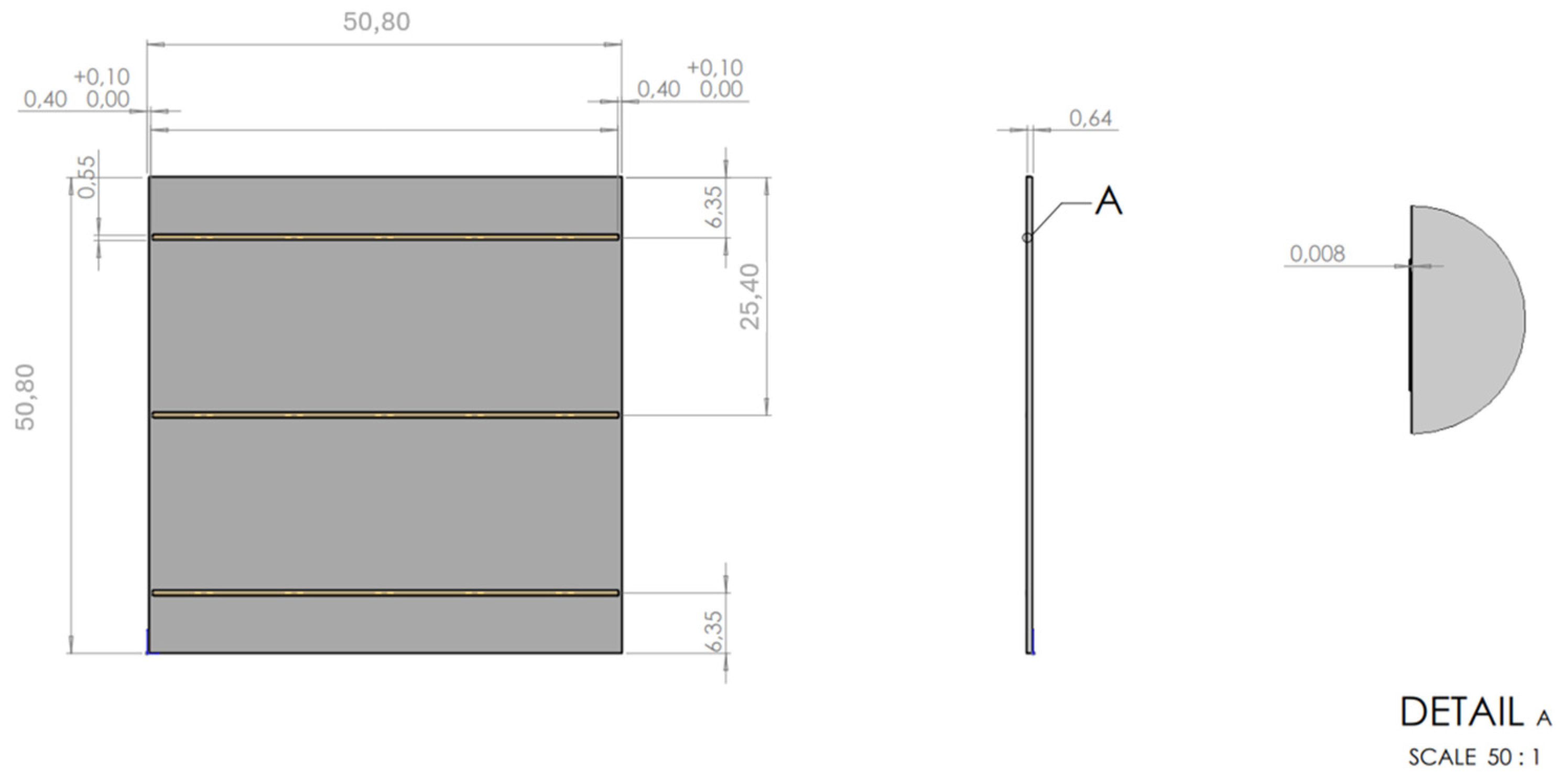
Figure 2.
SEM and EDS results, with particle size measurements of the AuNPs in dried form and in the prepared dispersion.
Figure 2.
SEM and EDS results, with particle size measurements of the AuNPs in dried form and in the prepared dispersion.
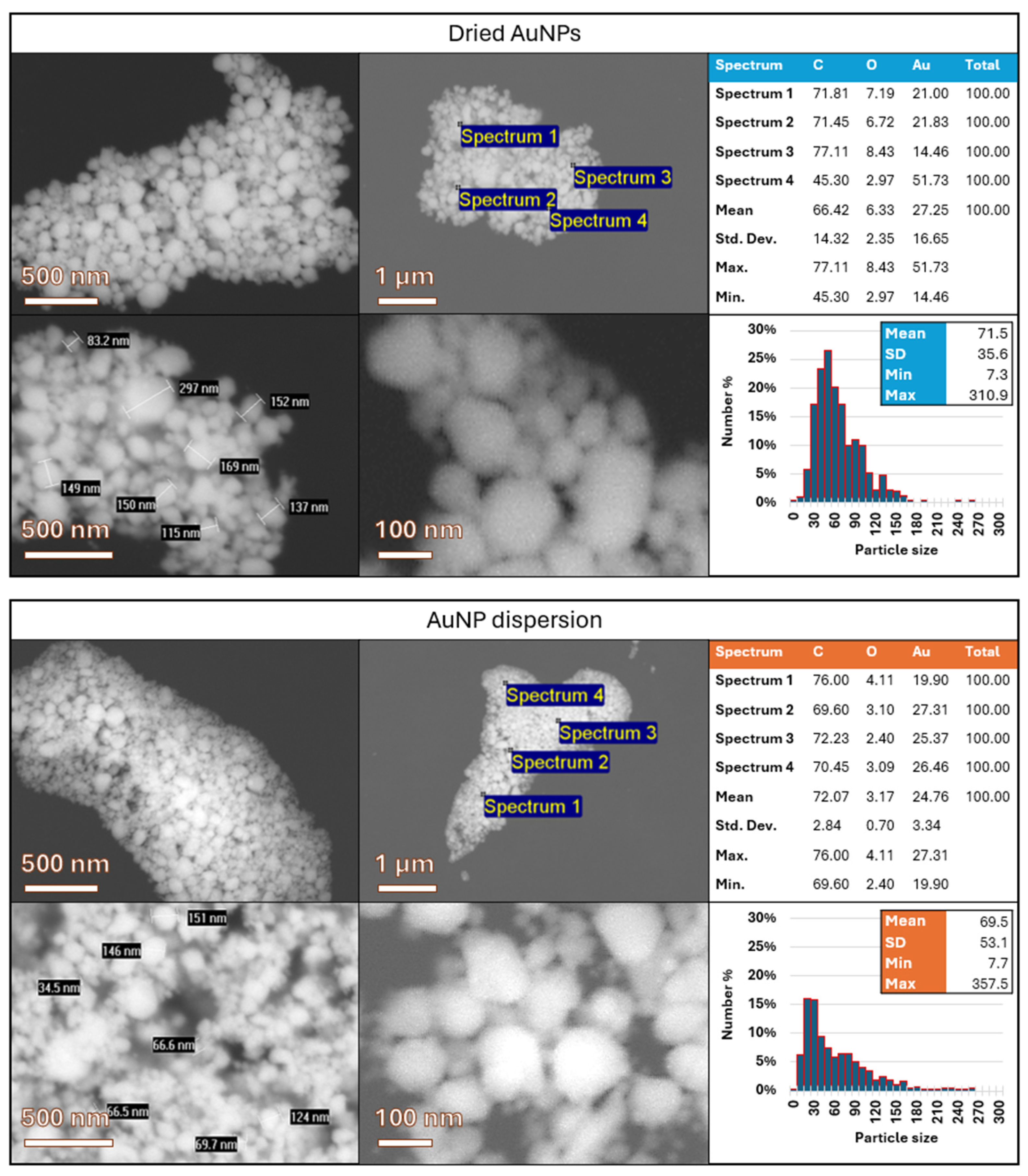
Figure 3.
Bright-field (BF) TEM images of the dried AuNPs: (a) Low-magnification image with (b) selected area electron diffraction (SAED) pattern corresponding to the AuNPs marked by a yellow circle in (a). (c) High-magnification image of the AuNPs with an inset showing the 2D Fast Fourier Transform (FFT) of a selected area in the high-resolution BF TEM image. (d) Scanning TEM (STEM)/EDS mapping of the dried AuNPs, with an inset displaying the EDS spectrum of the particle marked by a yellow square. Acceleration voltage: 200 kV.
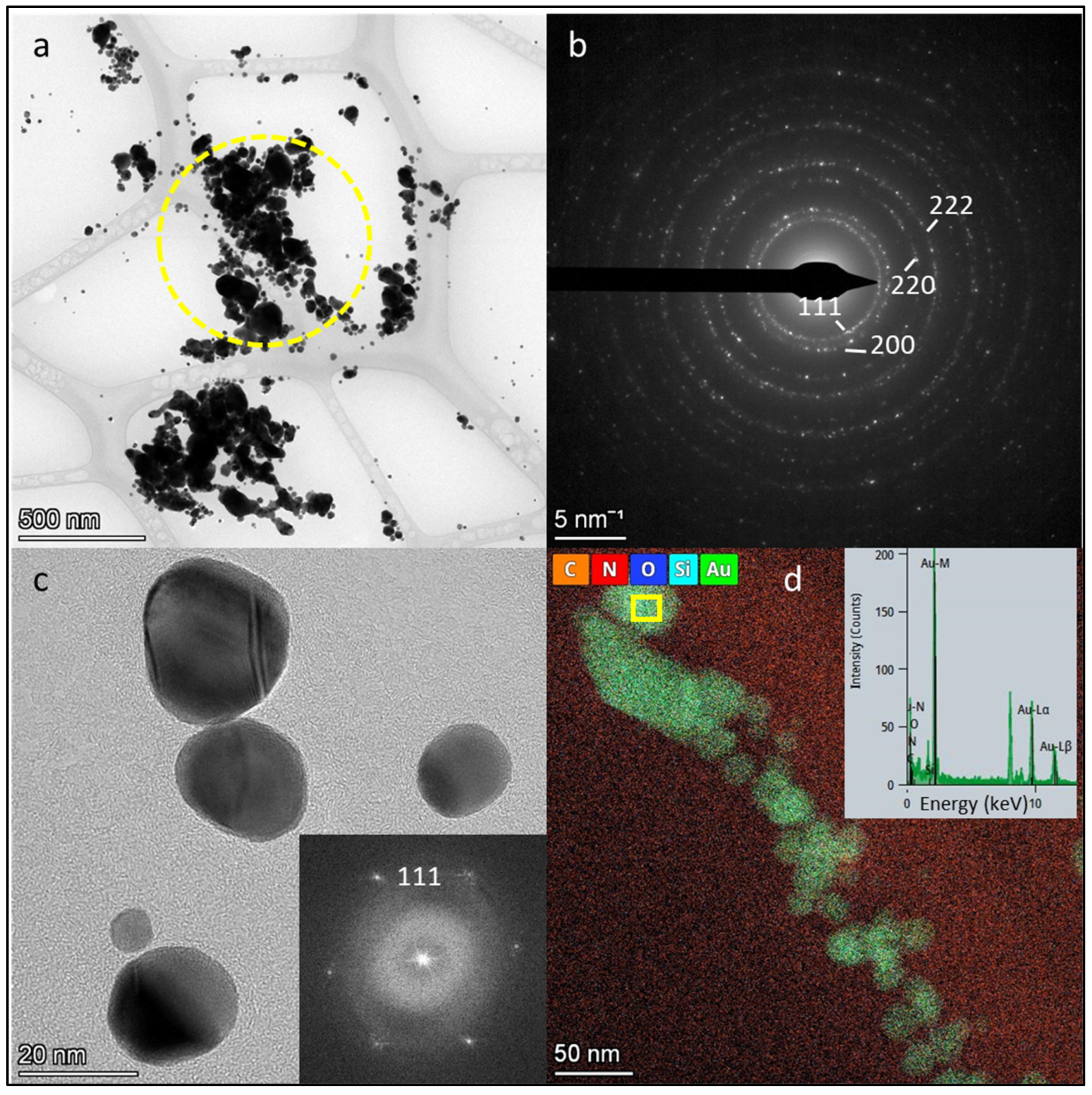
Figure 4.
UV-VIS absorbance spectra of the AuNPs dispersed in deionised water, pure deionised water and the difference between them.
Figure 4.
UV-VIS absorbance spectra of the AuNPs dispersed in deionised water, pure deionised water and the difference between them.
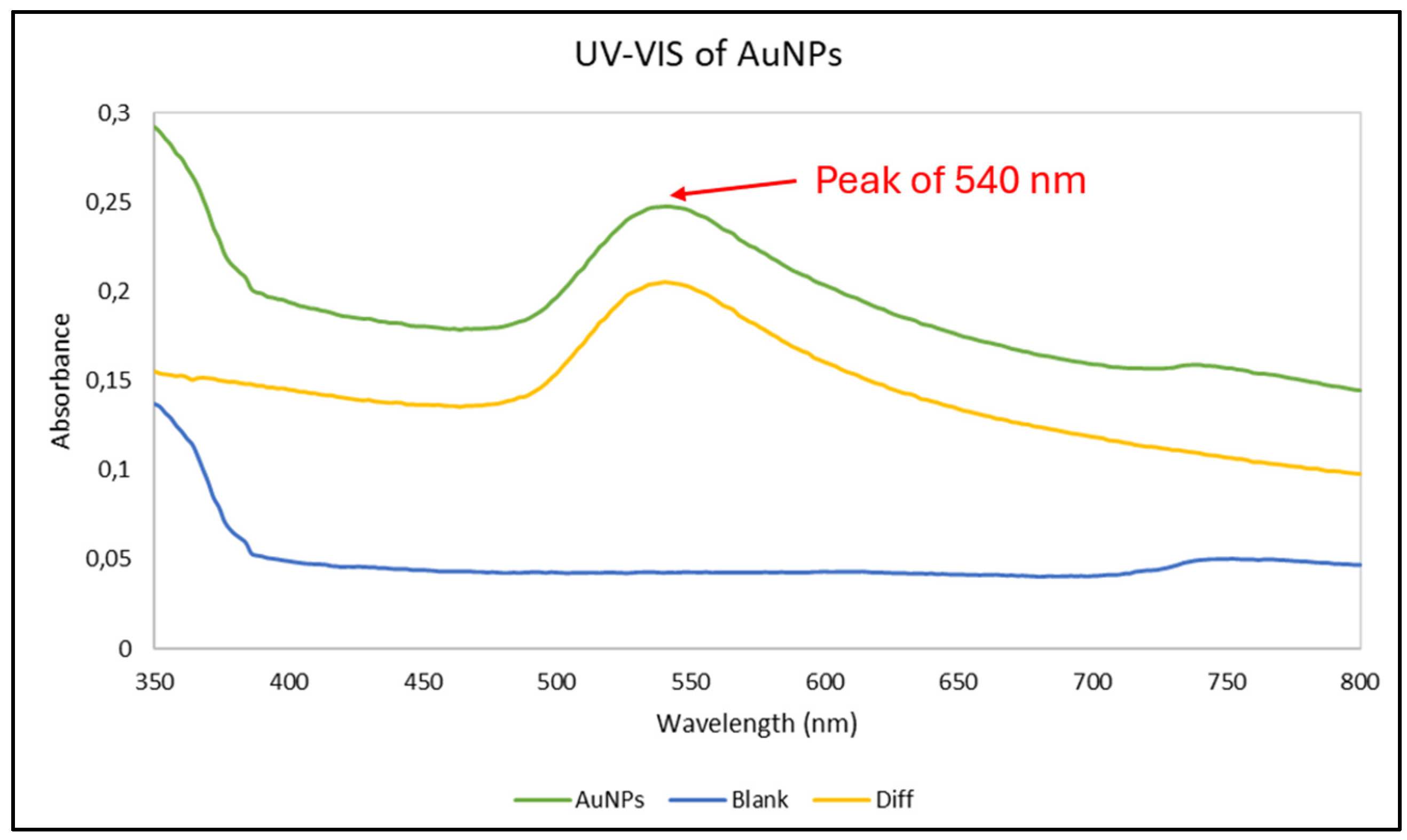
Figure 5.
DLS measurement results show the average particle diameter.
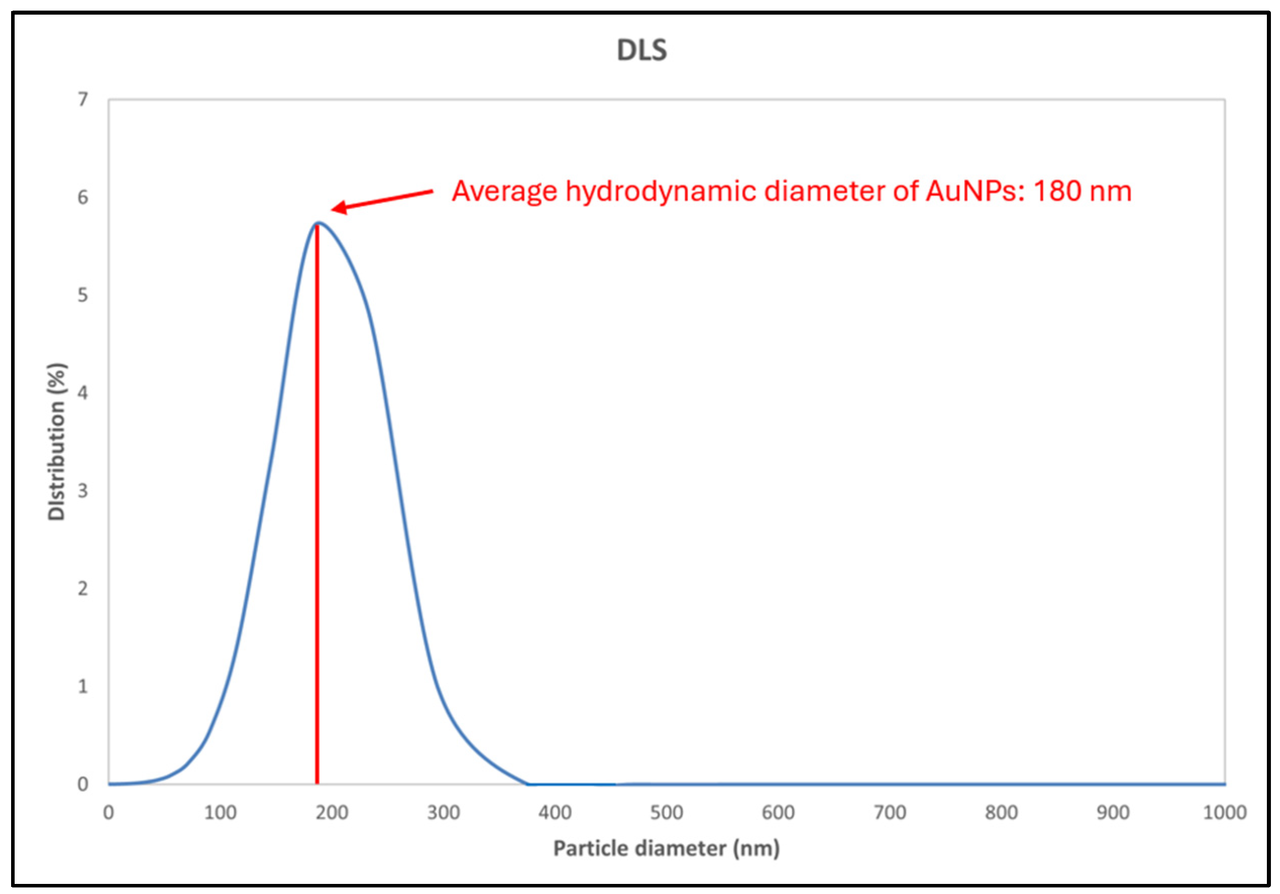
Figure 6.
Zeta potential results of the AuNPs in deionised water.
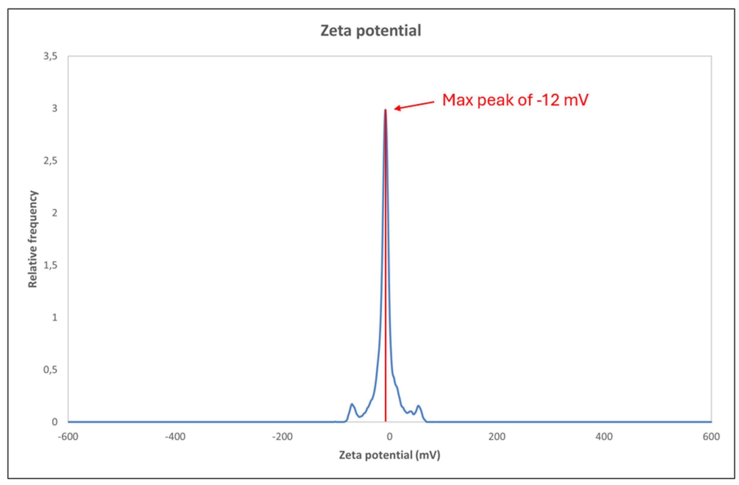
Figure 7.
TGA curve of the AuNPs` dispersion.
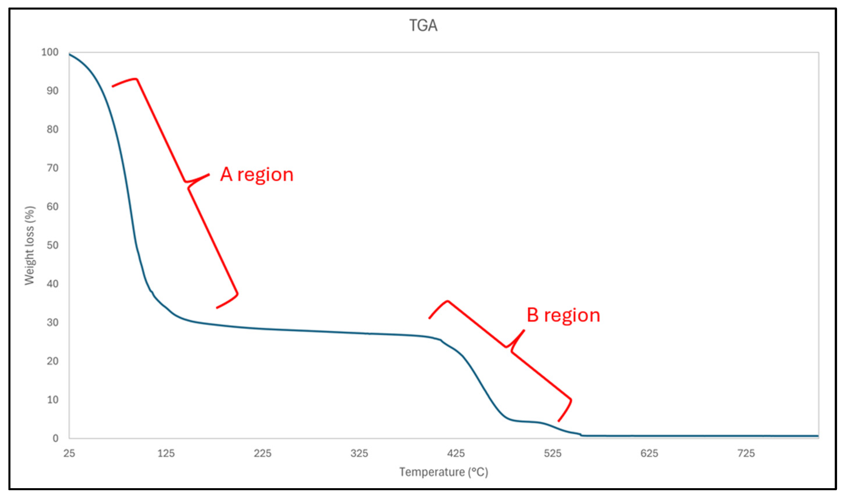
Figure 8.
Thixotropy of the AuNPs` dispersion.
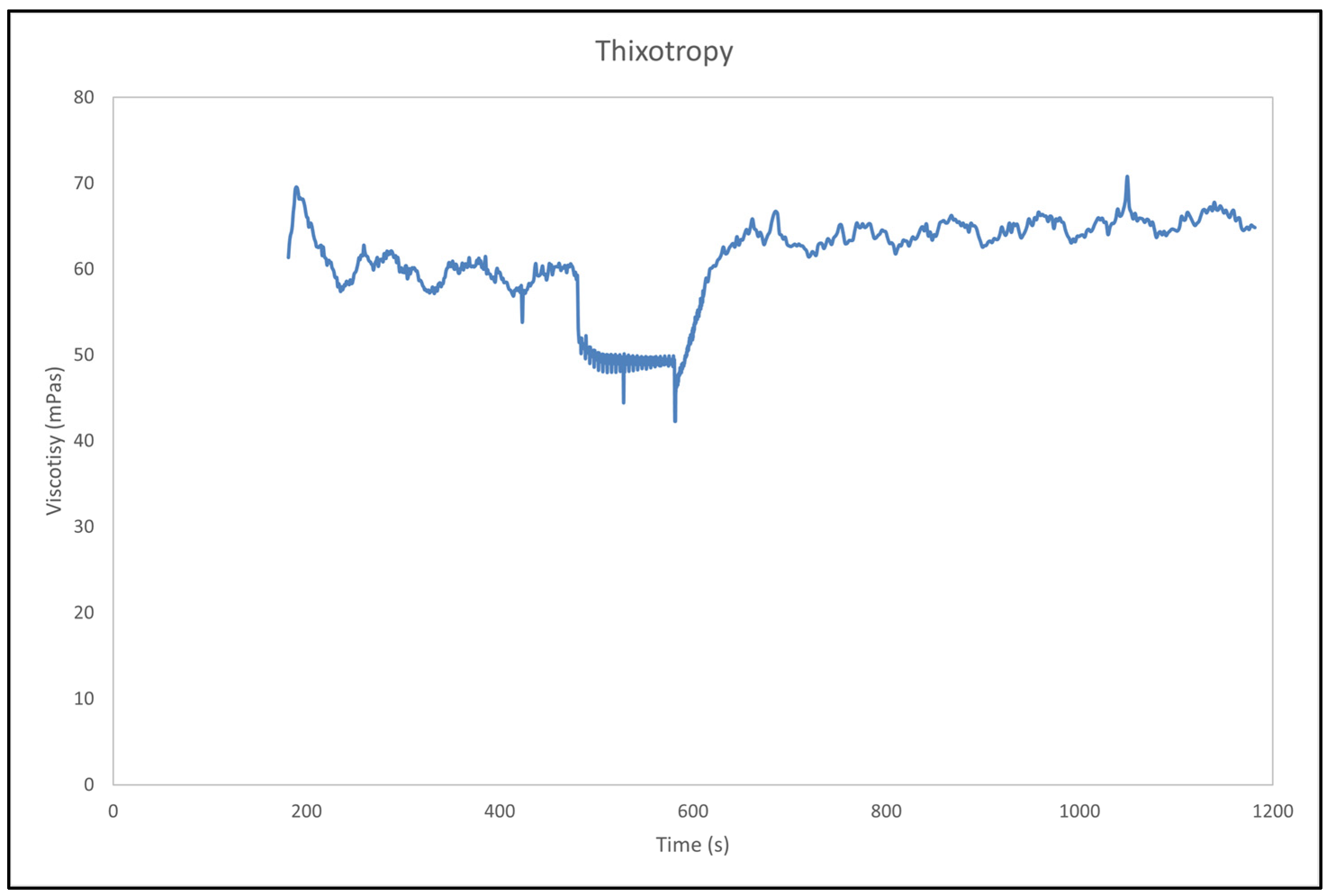
Figure 9.
(a), (b) and (c): unsuccessful plasma printing after the first trial.
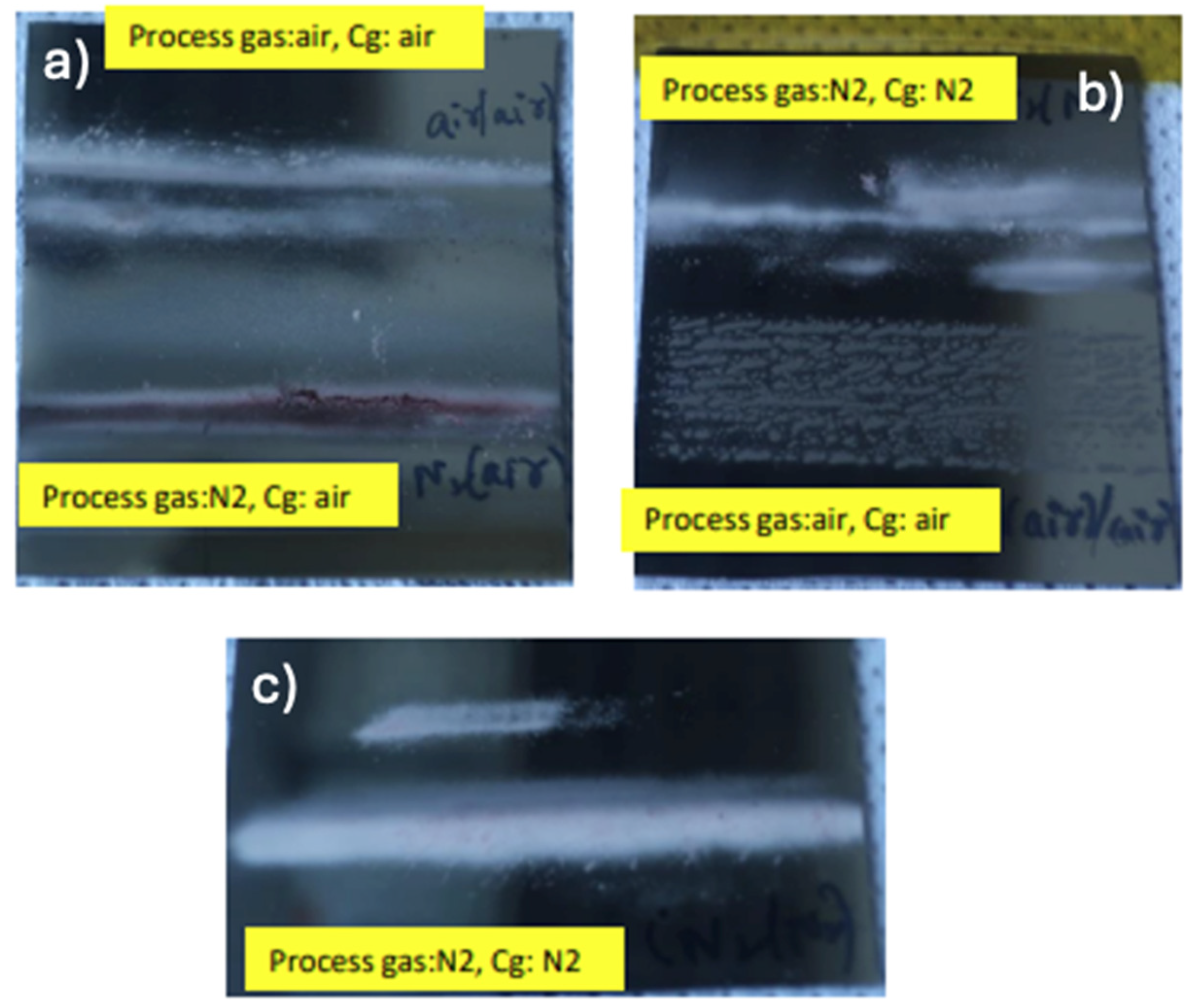
Figure 10.
(a) a close-up of one printed line, (b) printed substrate (c) SEM image of one line with visible areas for EDS analyses.
Figure 10.
(a) a close-up of one printed line, (b) printed substrate (c) SEM image of one line with visible areas for EDS analyses.
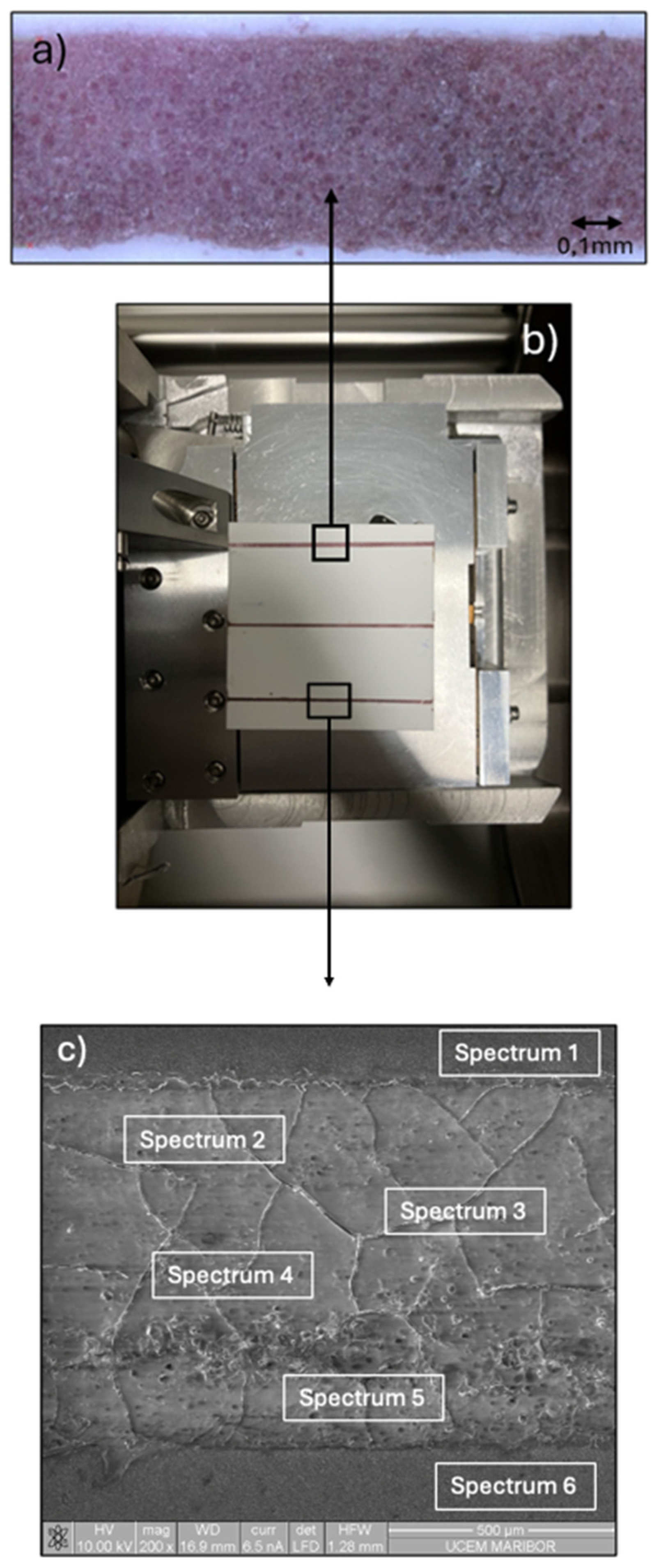
Figure 11.
Surface roughness results, showing the height profile (left), a 3D topographic image of the surface (middle) and the Sa values (right).
Figure 11.
Surface roughness results, showing the height profile (left), a 3D topographic image of the surface (middle) and the Sa values (right).
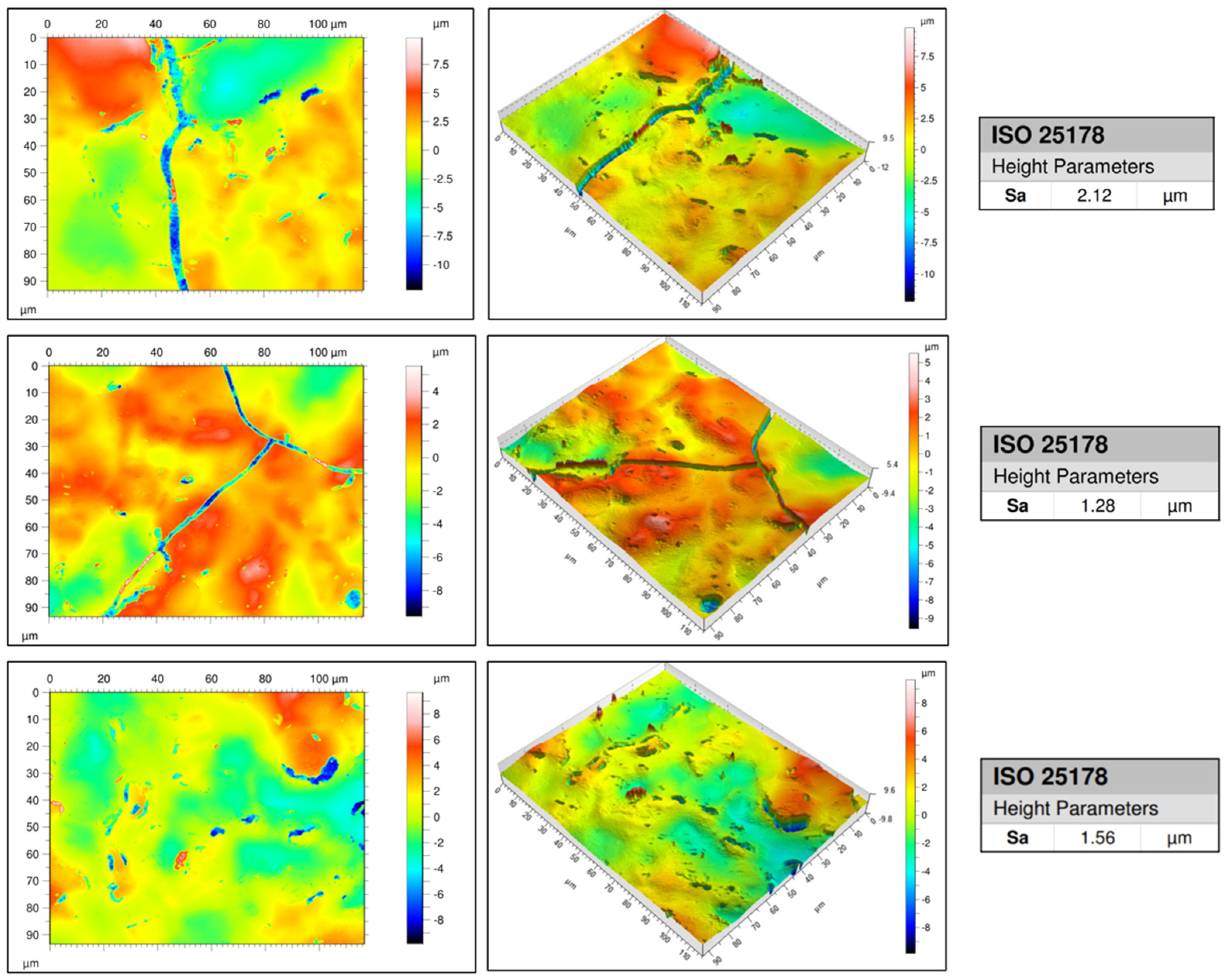

Table 1.
ICP-OES analysis of the Au concentration after USP and in the AuNPs` dispersion.
| Sample name | mg/ml Au |
| AuNPs` suspension | 2,81 |
| AuNPs` dispersion | 0,246 |
Table 2.
Statistical analysis of the DLS measurements.
| Results | AuNPs |
| Hydrodynamic diameter | 180 nm |
| Polydispersity index | 25 % |
| Standard Deviation | 2.93 nm |
Table 3.
EDS analysis of the printed line.
| Spectrum | C | O | Al | Au | |
| Spectrum 1 | 19.74 | 51.64 | 27.21 | / | |
| Spectrum 2 | 75.23 | 24.59 | / | 0.18 | |
| Spectrum 3 | 76.42 | 22.88 | / | 0.70 | |
| Spectrum 4 | 83.80 | 15.18 | / | 1.02 | |
| Spectrum 5 | 75.29 | 24.05 | / | 0.33 | |
| Spectrum 6 | 5.62 | 56.46 | 37.91. | / |
Disclaimer/Publisher’s Note: The statements, opinions and data contained in all publications are solely those of the individual author(s) and contributor(s) and not of MDPI and/or the editor(s). MDPI and/or the editor(s) disclaim responsibility for any injury to people or property resulting from any ideas, methods, instructions or products referred to in the content. |
© 2025 by the authors. Licensee MDPI, Basel, Switzerland. This article is an open access article distributed under the terms and conditions of the Creative Commons Attribution (CC BY) license (http://creativecommons.org/licenses/by/4.0/).
Copyright: This open access article is published under a Creative Commons CC BY 4.0 license, which permit the free download, distribution, and reuse, provided that the author and preprint are cited in any reuse.


