Submitted:
29 April 2025
Posted:
29 April 2025
You are already at the latest version
Abstract
Nanostructure-based coloration has been investigated extensively to overcome the limitations of conventional pigments and dyes. In this study, we focused on the dynamic coloration of plasmonic structures via the photothermal deformation of a metal semi-shell. However, identifying the optimal structure using this method typically requires considerable computational time. To address this challenge, we proposed an approach for estimating the optimal structure that reduced computational demands. The color-gamut area is influenced by both the density of the nanospheres and the thickness of the semi-shell. The deformation of the shell due to laser-induced local heating was simulated at various irradiation intensities. The results indicated that the semi-shell thickness that maximized the gamut area for a given nanosphere diameter and density was strongly correlated with both the diameter and density. The estimation of the optimal nanostructure is expected to facilitate the efficient fabrication of dynamic plasmonic color materials.
Keywords:
plasmonic color
; photothermal deformation
; metal semi-shell nanostructure
; discrete dipole approximation
1. Introduction
Ultraviolet light, toxicity concerns, and the challenge of coloring submicron areas pose significant obstacles in the field of coloration. Although photonic crystals and dielectric multilayers have been explored to address these problems, they face limitations, such as low reflectance and a restricted range of color variation. Metallic nanostructures are considered to be promising solutions to these challenges. For example, periodic nanodiscs and nanoholes can produce stable colors with a high spatial resolution over extended periods; however, these colors cannot be modified after fabrication. Various methods can dynamically change structural color, including polarizing [1,2], electrifying [3,4], heating [5,6], triggering chemical reactions [7], and applying mechanical techniques [8]. Each approach has distinct advantages over the conventional coloration methods. However, they face several limitations, including the requirement for electron beam lithography, which is complicated and limited to small areas [1,7], reliance on electricity [3,4], requirement of stress and deformation [8], and restricted color range [5,6].
Previous studies have demonstrated that dynamic plasmonic coloring utilizing a metal semi-shell structure facilitates the efficient and cost-effective processing of large areas and exhibits the potential to achieve a broad color gamut [9]. In this study, the reflection spectra were computed using the discrete dipole approximation (DDA) for various diameters and densities of the nanospheres, thicknesses of the metal semi-shells, and shapes of the capping angles of the metal semi-shells. The color-gamut area was defined as the polygonal region on the chromaticity diagram delineated by multiple coordinates derived from the reflection spectra. The color-gamut area is influenced by both the density of the nanospheres and the thickness of the semi-shell. Before depositing the semi-shell, the thickness that maximizes the color-gamut area, which depends on the density of the nanospheres, must be estimated. The chromaticity coordinates were determined via time-consuming DDA calculations performed for each combination of the nanosphere diameter, density, semi-shell thickness, and capping angle of the semi-shell. For example, calculations for a nanosphere with diameters, densities, semi-shell thicknesses, and capping angles of 100 nm, 19.8 µm−2, 20 nm, and 90°, respectively, required 23 h and 25 min when using DDSCAT7.3.3 [10] software on an Intel Core i7-8700 3.2 GHz processor. To reduce the computational time, estimating the semi-shell thickness that optimizes the color-gamut area for specific values of nanosphere diameter and density is advantageous.
This study demonstrates that the semi-shell thickness that maximizes the gamut area for a given nanosphere diameter and density is strongly correlated with both the diameter and density.
2. Materials and Methods
The calculations included the incident angle, polarization, wavelength, nanostructure material and shape, chromaticity coordinates, and the evaluation index by area on a chromaticity diagram. The metal semi-shell structures considered in this study are typically fabricated by immersing a substrate in a liquid containing dispersed nanospheres, which allows the nanospheres to adhere to the substrate and then deposit metal onto the nanospheres.
2.1. Materials and Structure
The core material was fused silica, which was chosen because of its heat resistance and widespread availability. Aluminum was selected as the substrate material because of its cost-effectiveness and widespread availability. Silver was used as the deposition material to achieve the broadest color gamut, as demonstrated in previous studies [9]. The refractive indices of fused silica, aluminum, and silver were obtained from literature [11,12,13]. The diameters of the nanospheres were 50, 75, and 100 nm, and the substrate thickness was 40 nm. The deposition thicknesses and densities are listed in Table 1. The capping angles of the semi-shells varied by 30°, 40°, 45°, 50°, 55°, 60°, 65°, 70°, 80°, and 90°.
2.2. Reflectance Spectrum
Figure 1(a) illustrates the reflection of incident light from a nanostructure composed of a substrate, nanospheres, and a metal semi-shell. The deformation of the shell owing to laser-induced local heating was simulated at various irradiation intensities. Upon laser irradiation, the metal semi-shell underwent local heating, leading to melting and deformation driven by surface tension [14]. The capping angle varied from 90° to 30° (Figure 1(b)). The reflectance spectra were calculated using the DDA method with DDSCAT 7.3.3 software [10]. The wavelength varied from 380 to 780 nm in increments of 10 nm. The refractive index of the surrounding medium was set as 1.0, and two orthogonal incident polarizations, each at an incidence angle of 0°, were applied to the nanostructures. The resulting reflection spectra are shown in Figure 1(c).
2.3. Calculation Condition
For the DDA calculations, the dipole spacing was set to 2 nm. The densities of the nanostructures are listed in Table 1. Because the nanoparticles were placed closer to the substrate than to their neighboring nanoparticles, the plasmon coupling between the nanoparticles and the substrate was stronger than that between the nanoparticles themselves [15]. Consequently, the absorption characteristics of the periodic structure closely resembled those of a random structure.
2.4. Gamut Area in Commission Internationale de l’Éclairage (CIE) Luv Color Space
The tristimulus values, XYZ, of the light were calculated from the reflectance spectrum R(λ) at each capping angle, CIE standard light source D65 spectrum I(λ), and isochromatic function of the CIE 1931, 2° colorimetric standard observer [16,17], which represents the average human color perception over a 2° visual field, as expressed by Equation (1):
Here, and are the CIE 1931 color-matching functions of a 2° observer (Figure 1(d)) [18]. The values in the CIE XYZ color space were then converted to the CIE Luv color space (Figure 1(e)), as follows [19]:
The area S enclosed by the coordinate points derived from the reflectance spectra of all capping angles in the CIE Luv color space, calculated using Equation (3), was adopted as the evaluation criterion [20].
3. Results
3.1. Gamut Areas in the CIE Luv Chromaticity Diagram
Figure 2(a)–(c) show the gamut areas in the CIE Luv chromaticity diagrams. The x-axis represents the density, whereas the y-axis depicts the color-gamut area within the CIE Luv color space. The values following the capital letter “D” in the legend correspond to the nanosphere diameter in nanometers (nm), whereas those following the lowercase letter “d” indicate the shell thickness in nanometers (nm). For each nanosphere diameter and shell thickness, the color-gamut area was maximized at a specific density.
3.2. Density of the Maximum Gamut Area for Each Core Diameter and Shell Thickness
The color-gamut area corresponding to each nanosphere and shell thickness was fitted using a Gaussian function. The central values of the resulting Gaussian functions are listed in Table 2. This central value was identified as the point at which the color-gamut area reached its maximum value. These data points were approximated using the equation for a plane (4):
The following coefficients and determination coefficient were obtained:
The data were sufficiently approximated by a plane, as illustrated in Figure 2(d).

Table 2.
Best density for each nanostructure.
| Core diameter [nm] | Shell thickness [nm] | Density [µm−2] | Center-to-center distance [nm] |
|---|---|---|---|
| 50 | 17.5 | 163.325 ± 2.064 | 78.2 |
| 50 | 20 | 101.986 ± 0.663 | 99.0 |
| 75 | 15 | 48.396 ± 0.173 | 143.7 |
| 75 | 20 | 39.089 ± 0.048 | 159.9 |
| 75 | 25 | 32.759 ± 0.160 | 174.7 |
| 100 | 15 | 24.141 ± 0.053 | 203.5 |
| 100 | 20 | 19.734 ± 0.198 | 225.1 |
| 100 | 25 | 15.838 ± 0.052 | 251.3 |
4. Discussion
4.1. Validation of the Approximation Formula
In the case of a core diameter of 75 nm and density of 45.0 µm−2, which corresponds to a center-to-center distance of 149.0 nm, the maximum gamut area obtained using the approximate formula (4) was 17.5 nm in semi-shell thickness. Figure 3(a) illustrates the calculated gamut area for a core diameter of 75 nm and a semi-shell thickness of 17.5 nm. Additionally, the figure demonstrates that the densities at which the gamut area reached its peak are almost identical. Moreover, as summarized in Table 3 and illustrated in Figure 3(b), point (75, 149.0, 17.5) lies closer to the fitted plane than the data points used to construct the plane. This proximity confirms the validity of the estimation.
4.2. Structure that Maximizes the Gamut Area
To expand the gamut area, the reflectance trough values appearing at each capping angle must be as close as possible to zero. For example, Figure 3(b) shows the reflectance spectra at each capping angle for a core diameter of 75 nm, semi-shell thickness of 20 nm, and center-to-center distance of 140 nm. At a capping angle of 70°, a reflectance trough appears at a wavelength of 0.58 µm. Figure 3(c) shows the relationship between the center-to-center distance and the absorption efficiency Qabs for a core diameter of 75 nm, shell thickness of 20 nm, and capping angle of 70°. The decrease in Qabs with increasing distance can be explained by the decrease in the absorption efficiency per unit area owing to a decrease in the nanostructure density. However, the decrease in Qabs with increasing distance can be explained by the fact that when the nanostructures are too close together, the absorption due to plasmon resonance broadens [21], and the reflectivity does not decrease to zero. At this distance, which is significantly smaller than the wavelength of light, the red and blue shifts in the light absorption peak resulting from the plasmon coupling between the nanoparticles become more prominent, depending on the polarization direction of the incident light. Because the present calculations were based on unpolarized light, both red and blue shifts were obtained. The extent of broadening of the absorption peak increased with decreasing distance. As the absorption peak broadened, the reflectance trough became shallower and the chromaticity coordinates approached white, thereby reducing the area occupied in the chromaticity diagram.
5. Conclusions
In this study, we propose a method for estimating the optimum thickness of the metal deposited in advance to widen the color gamut of plasmonic colors produced by nanostructures. These nanostructures are fabricated by dipping a substrate in a liquid containing dispersed nanospheres, which causes them to adhere to the substrate and then depositing the metal on top of them. The color-gamut area is influenced by both the density of the nanospheres and the thickness of the semi-shell. The deformation of the shell owing to laser-induced local heating was simulated at various irradiation intensities. The results showed that the semi-shell thickness that maximized the gamut area for a given nanosphere diameter and density was strongly correlated with both the diameter and density. To reduce computational time, it is advantageous to estimate the semi-shell thickness that optimizes the color-gamut area for specific values of nanosphere diameter and density. The proposed estimation of the optimal nanostructure should enable efficient fabrication of dynamic plasmonic color materials. Further research is required to validate the proposed approach.
Author Contributions
Conceptualization, R.F. and M.M.; Data curation, M.M.; Formal analysis, R.F. and M.M.; Funding acquisition, M.M.; Investigation, M.M.; Methodology, R.F. and M.M.; Project, R.F. and M.M.; Resources, R.F. and M.M.; Software, R.F. and M.M.; Supervision, R.F.; Validation, R.F. and M.M.; Visualization, M.M.; Writing - original draft, M.M.; Writing - review & editing, R.F. and M.M.
Funding
The APC was funded by MDPI.
Data Availability Statement
The raw data supporting the conclusions of this article will be made available by the authors on request.
Acknowledgments
We would like to thank Editage [http://www.editage.com] for editing and reviewing this manuscript for English language.
Conflicts of Interest
The authors declare no conflicts of interest.
Abbreviations
| MDPI | Multidisciplinary Digital Publishing Institute |
References
- Ellenbogen, T.; Seo, K.; Crozier, K.B. Chromatic plasmonic polarizers for active visible color filtering and polarimetry. Nano Lett. 2012, 12, 1026–1031. [Google Scholar] [CrossRef] [PubMed]
- Song, M.; Li, X.; Pu, M.; Guo, Y.; Liu, K.; Yu, H.; Ma, X.; Luo, X. Color display and encryption with a plasmonic polarizing metamirror. Nanophotonics 2018, 7, 323–331. [Google Scholar] [CrossRef]
- Xiang, J.; Li, Y.; Li, Q.; Paterson, D.A.; Storey, J.M.-D.; Imrie, C.T.; Lavrentovich, O.D. Electrically tunable selective reflection of light from ultraviolet to visible and infrared by heliconical cholesterics. Adv. Mater. 2015, 27, 3014–3018. [Google Scholar] [CrossRef] [PubMed]
- Mirshafieyan, S.S.; Gregory, D.A. Electrically tunable perfect light absorbers as color filters and modulators. Sci. Rep. 2018, 8, 2635. [Google Scholar] [CrossRef] [PubMed]
- Shu, F.-Z.; Yu, F.-F.; Peng, R.-W.; Zhu, Y.-Y.; Xiong, B.; Fan, R.-H.; Wang, Z.-H.; Liu, Y.; Wang, M. Dynamic plasmonic color generation based on phase transition of vanadium dioxide. Adv. Opt. Mater. 2018, 6, 1700939. [Google Scholar] [CrossRef]
- Prezgot, D.; Tatarchuk, S.W.; Ianoul, A. Plasmonic color generation in silver nanocrystal-over-mirror films by thermal embedment into a polymer spacer. Nano Select 2022, 3, 1082–1090. [Google Scholar] [CrossRef]
- Duan, X.; Kamin, S.; Liu, N. Dynamic plasmonic colour display. Nat. Commun. 2017, 8, 14606. [Google Scholar] [CrossRef] [PubMed]
- Song, S.C.; Ma, X.L.; Pu, M.B.; Li, X.; Liu, K.P.; Gao, P.; Zhao, Z.Y.; Wang, Y.Q.; Wang, C.T.; Luo, X.G. Actively tunable structural color rendering with tensile substrate. Adv. Opt. Mater. 2017, 5, 1600829. [Google Scholar] [CrossRef]
- Magari, M.; Fujimura, R. Numerical investigation of dynamic plasmonic color generated via photothermal deformation of a metal semi-shell structure. Jpn. J. Appl. Phys 2024, 63, 082001. [Google Scholar] [CrossRef]
- Draine, B.T.; Flatau, J. Discrete-dipole approximation for scattering calculations. J. Opt. Soc. Am. A 1994, 11, 1491–1499. [Google Scholar] [CrossRef]
- Malitson, I.H. Interspecimen comparison of the refractive index of fused silica. J. Opt. Soc. Am. 1965, 55, 1205–1209. [Google Scholar] [CrossRef]
- Polyanskiy, M.N. Refractiveindex.info database of optical constants. Sci. Data 2024, 11, 94. [Google Scholar] [CrossRef] [PubMed]
- Rakic, A.D.; Djurisic, A.B.; Elazar, J.M.; Majewski, M.L. Optical properties of metallic films for vertical-cavity optoelectronic devices. Appl. Opt. 1998, 37, 5271–5283. [Google Scholar] [CrossRef] [PubMed]
- Fujimura, R.; Zhang, R.; Kitamoto, Y.; Shimojo, M.; Kajikawa, K. Modeling of semi-shell nanostructures formed by metal deposition on dielectric nanospheres and numerical evaluation of plasmonic properties. Jpn. J. Appl. Phys. 2014, 53, 03520. [Google Scholar] [CrossRef]
- Chevalier, P.; Bouchon, P.; Jaeck, J.; Lauwick, D.; Bardou, N.; Kattnig, A.; Pardo, F.; Haïdar, R. Absorbing metasurface created by diffractionless disordered arrays of nanoantennas. Appl. Phys. Lett. 2015, 107, 251108. [Google Scholar] [CrossRef]
- Smith, T.; Guild, J. The C.I.E. colorimetric standards and their use. Trans. Opt. Soc. 1931, 33, 73. [Google Scholar] [CrossRef]
- Ohta, N.; Robertson, A.R. CIE Standard Colorimetric System. In Colorimetry: Fundamentals and Applications; Kriss, M.A., Ed.; Wiley: England, 2005. [Google Scholar]
- CIE. CIE 1931 Colour-Matching Functions, 2 Degree Observer (Data Table). International Commission on Illumination (CIE): Vienna, Austria, 2018. [Google Scholar]
- Carter, E.C.; et al. CIE 015:2018 Colorimetry 4th edition. Commission Internationale de l'Eclairage: Vienna, Austria, 2018. [Google Scholar]
- Braden, B. The surveyor's area formula. College Math. J. 1986, 17, 326–337. [Google Scholar] [CrossRef]
- Jain, P.K.; Huang, W.; El-Sayed, M.A. On the universal scaling behavior of the distance decay of plasmon coupling in metal nanoparticle pairs: A plasmon ruler equation. Nano Lett. 2007, 7, 2080–2088. [Google Scholar] [CrossRef]
Figure 1.
(a) Schematic of reflection of incident light from the structure. (b) Capping angles and unit structures. (c) Reflectance spectra corresponding to a diameter of 75 nm, semi-shell thickness of 20 nm, and a center-to-center distance of 165 nm. (d) CIE1931 color matching functions of a 2° observer. (e) Change in the color gamut of Ag shells of 20-nm thickness on silica cores of 75 nm on Al substrate at a density of 36.7 μm–2 as the capping angle decreases from 90° to 30° in the CIE Luv chromaticity diagram.
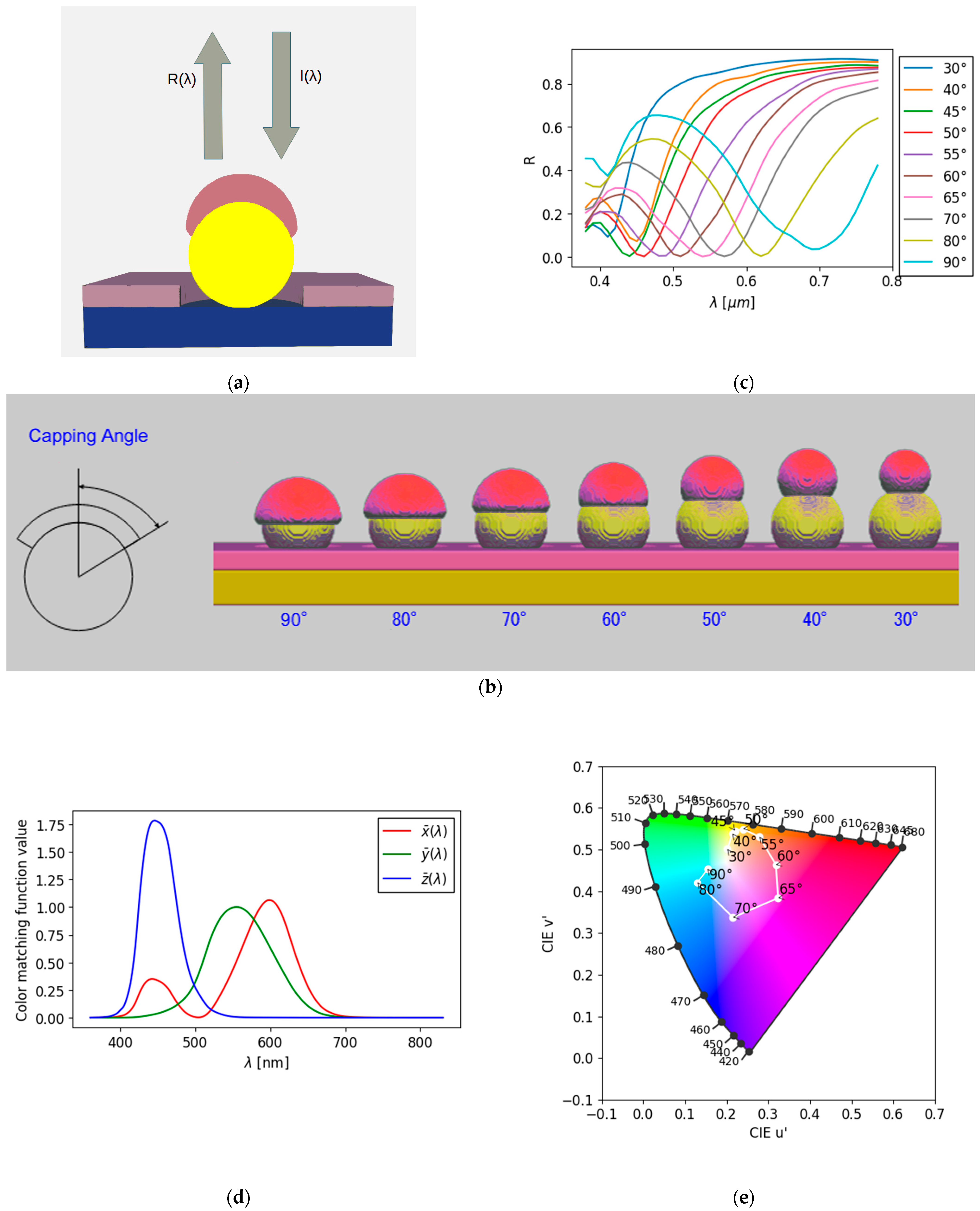
Figure 2.
Gamut areas in CIE Luv color space for (a) core diameter of 50 nm and shell thicknesses of 17.5 nm and 20 nm; (b) core diameter of 75 nm and shell thicknesses of 15, 20, and 25 nm; and (c) core diameter of 100 nm and shell thicknesses of 15, 20, and 25 nm. (d) Core diameter, period, and shell thickness for the maximum gamut area. x-axis: core diameter [nm], y-axis: period [nm], and z-axis: shell thickness [nm].
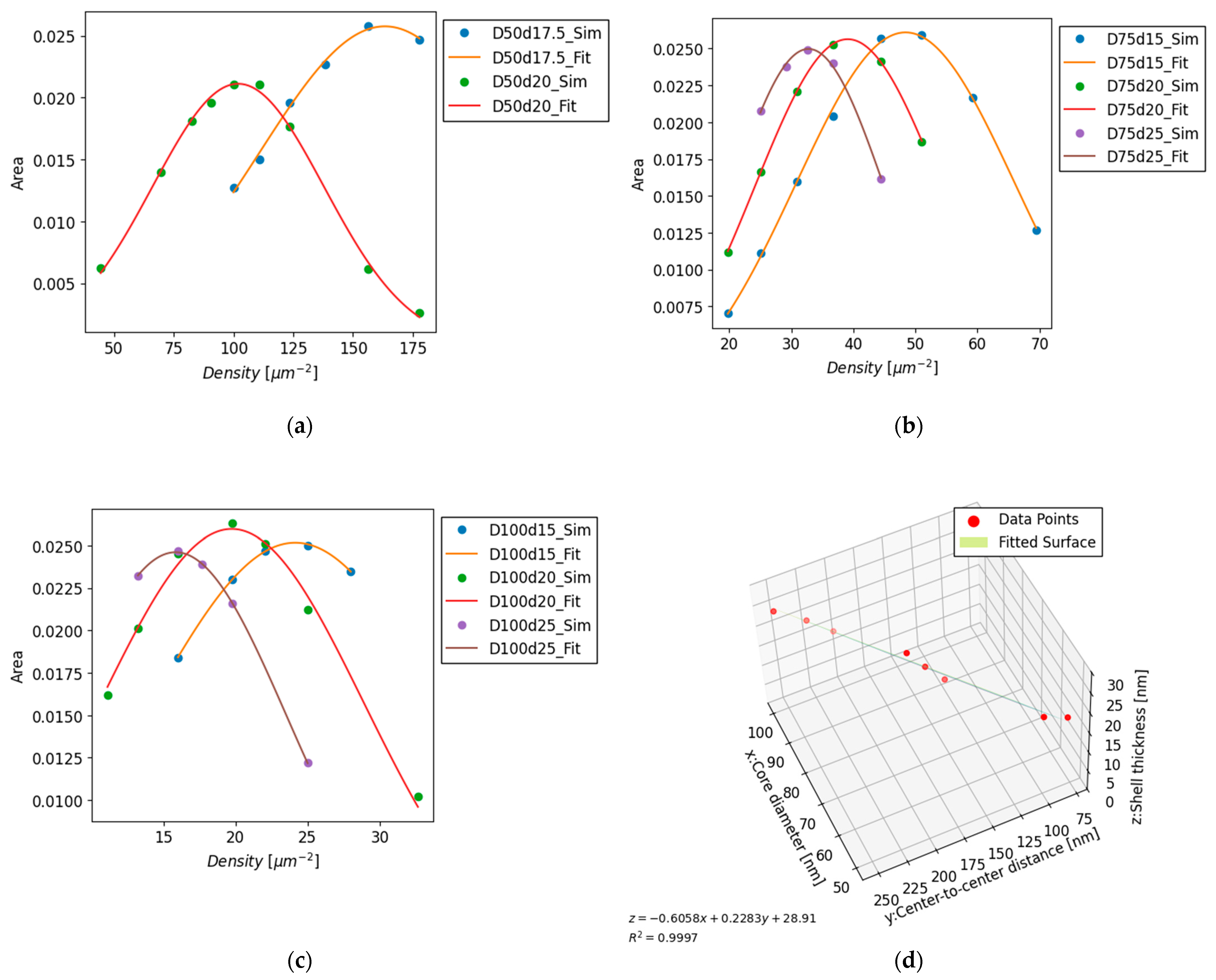
Figure 3.
(a) Gamut area in the CIE Luv color space for a core diameter of 75 nm and a shell thickness of 17.5 nm. (b) Predicted data obtained from new simulation of estimated plane. (c) Reflectance spectra at core diameter of 75 nm, shell thickness of 20 nm, and center-to-center distance of 140 nm. The trough of the reflectance spectrum at a wavelength of 0.58 µm at a capping angle of 70° has a reflectance of approximately 0.1. (d) Absorption efficiency at a wavelength of 0.58 µm for a core diameter of 75 nm and shell thickness of 20 nm at a capping angle of 70°.
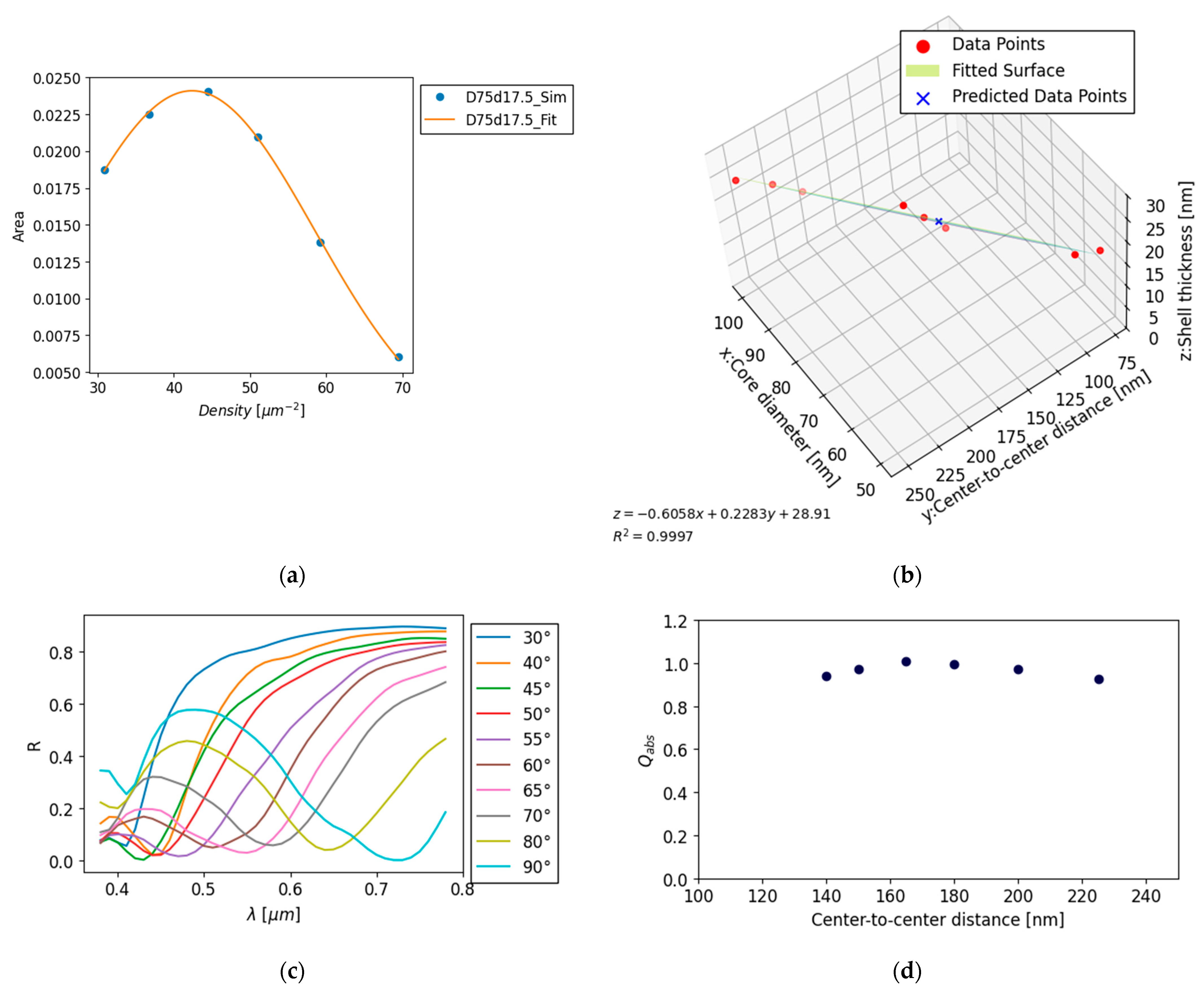
Table 1.
Dimensions of the nanostructures used for calculations.
| Diameter of nanosphere [nm] | Density [µm−2] | Deposition thickness [nm] |
|---|---|---|
| 50 | 44.4–177.8 | 17.5, 20 |
| 75 | 19.8–59.2 | 15, 20, 25 |
| 100 | 11.1–32.7 | 15, 20, 25 |
Table 3.
Best density for each nanostructure.
| Core diameter [nm] | Shell thickness [nm] (a) | Center-to-center distance [nm] | Approximated thickness [nm] (b) | Difference between shell thickness and the approximated thickness [nm] (a)-(b) | |
|---|---|---|---|---|---|
| A | 50 | 17.5 | 78.2 | 16.473 | 1.027 |
| 50 | 20 | 99.0 | 21.222 | −1.222 | |
| 75 | 15 | 143.7 | 16.282 | −1.282 | |
| 75 | 20 | 159.9 | 19.980 | 0.020 | |
| 75 | 25 | 174.7 | 23.359 | 1.641 | |
| 100 | 15 | 203.5 | 14.789 | 0.211 | |
| 100 | 20 | 225.1 | 19.720 | 0.280 | |
| 100 | 25 | 251.3 | 25.702 | −0.702 | |
| B | 75 | 17.5 | 149.0 | 17.492 | 0.008 |
Note: A was used to calculate the plane and B was used for validation.
Disclaimer/Publisher’s Note: The statements, opinions and data contained in all publications are solely those of the individual author(s) and contributor(s) and not of MDPI and/or the editor(s). MDPI and/or the editor(s) disclaim responsibility for any injury to people or property resulting from any ideas, methods, instructions or products referred to in the content. |
© 2025 by the authors. Licensee MDPI, Basel, Switzerland. This article is an open access article distributed under the terms and conditions of the Creative Commons Attribution (CC BY) license (http://creativecommons.org/licenses/by/4.0/).
Copyright: This open access article is published under a Creative Commons CC BY 4.0 license, which permit the free download, distribution, and reuse, provided that the author and preprint are cited in any reuse.


