
Submitted:
25 April 2025
Posted:
28 April 2025
You are already at the latest version
Abstract
Placing printed conductive patterns onto nonplanar substrates is a challenging task. In this work we tested a simple method for depositing inkjet-printed conductive patterns on-to 3D-printed pieces with cavities and sharp edges. First, a silver nanoparticle ink was used to print conductive patterns onto a flexible and porous substrate made of electrospun polycaprolactone (PCL). Then, the printed patterns were transferred to 3D-printed pieces made of polylactic acid (PLA) by temperature-promoted adhesion. Finally, the printed patterns were cured to render them conductive. The influence of the number of printed layers on their electrical and mechanical properties was evaluated. The printed patterns were also transferred to flexible substrates such as thermoplastic polyurethane (TPU) and polyethylene terephthalate (PET) sheets achieving conductivity after curing. Moreover, the printed patterns were effective for modular interconnection among successive transferred patterns, since it was possible to achieve electrical contact between them during the trans-fer process.
Keywords:
printed electronics
; electrospinning
; 3D printing
; printed transfers
1. Introduction
The fabrication of devices and circuits onto nonplanar substrates is a challenge yet to overcome in order to trespass the prototype scale and jump to a more reliable and reproducible industrial production. Potential massive applications to nonplanar circuits are broad, including automotive, aerospace, wearables and skin electronics among many others.
Several approaches can be used for the fabrication of devices and circuits onto nonplanar substrates. Conductive tracks can be fabricated directly onto nonplanar surfaces by deposition of conductive materials using electrodeposition [1], plasma jet [2], vapor deposition, extrusion [3], inkjet or aerosol-jet printing [4]. For example, quantum dot LEDs could be already printed directly onto nonplanar surfaces by carefully selecting different combinations of materials [5]. Both approaches suffer from some drawbacks: a shadow mask or complex lithographic methods have to be used in order to print lines on the surface of a nonplanar piece whereas aerosol-jet and inkjet printing are slow on nonplanar substrates requiring very precise and complex numeric control (x, y, z, φ and θ) for printing onto 3D substrates. 3D printing is also being used for the fabrication of nonplanar circuits. In this case, the piece and the embedded circuit can be fabricated at the same time and thus seems to be the best approach in terms of degrees of freedom regarding design. 3D and inkjet printing have been used for the fabrication of batteries and interconnects by tailoring processes and nanocomposites with different functional materials [6,7,8,9]. However, fine line resolution is not achievable and performance of conductive materials for 3D printing must be further optimized. For instance, Izumi et al. developed a method called soft blanket gravure, which consist of transferring a gravure pattern to a soft blanket which in turn transfers it to the printing substrate. The highly deformable blanket allows transfer processes to nonplanar substrates. However, as the fidelity of the printed pattern depends on the printing pressure and the viscoelastic characteristics of the ink, this method must be carefully tuned for each ink and shape of the printing substrate [10].
On the other hand, circuits can be also printed onto planar substrates prior to molding them into a particular shape. For instance, Bakr et al. studied the integrity and functionality of copper conductive tracks deposited by on a flexible substrate after embedding it in a 3D plastic piece by injection molding using different plastics [11]. Another example of this approach is the work from Sundaram et al., which self-shaping substrates are 3D-printed, then electrically conductive patterns were inkjet-printed and finally the substrate self-folded once peeled off from the printing bed. This approach requires careful design of the 3D-printed substrate, and the achievable shapes are limited [12]. Special care must be taken in these cases to prevent cracking or delamination of the printed layers as it becomes very complex to match adhesion, mechanical and thermal properties between the substrate and the printed layers while maintaining functionality. Another variation of this approach consists of printing the circuit onto a planar, flexible and adhesive substrate which is stuck to the surface of a 3D or flexible object afterwards. This approach has been already used for in-mold-electronics, soft robots [13] and skin electronics. For instance, Miyamoto et al. fabricated an electrospun mat made of polyvinyl alcohol with deposited conductive tracks made of gold by vacuum deposition using a shadow mask [14]. This mat could be transferred to various substrates by dissolving the PVA with a water spray. Interestingly, a hydroprinting method for transferring conductive patterns from PVA films to 3D structures has been proposed.
Electrospinning is a very versatile technique for the fabrication of micro and nanoporous membranes for a wide variety of applications. It can be employed for the fabrication of nonwoven mats from a variety of materials, including thermoplastic polymers. Our group has been working on the fabrication of conductive electrospun mats based on polycaprolactone (PCL) for the fabrication of electronic devices [15,16]. PCL is a synthetic biodegradable polyester that has low glass transition temperature (-60 °C), low melting point (60 °C) and excellent flexibility.
Electrospun mats can be either planar or 3D-shaped, depending on the characteristics of the collector used. Moreover, electrospun fibers can be deposited as a surface layer onto 3D-printed objects. For instance, a recent paper from Saniei et al. reported the surface modification of 3D-printed screws made of polylactide (PLA) with electrospun fibers in order to improve their bioactivity [17].
Although it has been reported that conductive materials can be deposited onto electrospun mats and also electrospun mats can be used as surface layer onto 3D-printed objects in order to improve their functionality, inkjet printing of conductive materials onto electrospun mats and their use for transferring to 3D-printed objects has not been previously studied. In this work, a method for the fabrication of conductive tracks onto electrospun mats made of polycaprolactone (PCL) by inkjet printing is presented. These mats were transferred to different plastic planar and nonplanar surfaces by melting of the PCL, leaving the conductive track adhered and functional.
2. Materials and Methods
2.1. General Remarks
PCL (Mw 80000, Sigma-Aldrich), DMF and chloroform were reagent grade and used straight from the bottle. White PLA filament for 3D printing of 1.75 mm diameter was purchased to Grilon (Argentina). Baking paper, kraft paper and sulphite paper were purchased from a local seller. Silver nanoparticle ink DGP 40LT-15C from Advanced Nano Products was used.
2.2. Preparation of Polymer Solutions
1.2 g of PCL was dissolved in 10 ml of a mixture of chloroform:DMF 80:20 respectively under magnetic stirring for 4 hours. The solution has demonstrated stability for at least two weeks after preparation.
2.3. Fabrication of Electrospun Mats
A Y-flow electrospinner 2.2.D-500 (Y-flow SD, Spain) was used for electrospinning. Distance to the collector was optimized in order to obtain regular and dry fibers. Distance was determined as 26 cm as the optimum distance between the needle and the collector. The flow rate of the solution was 1 ml·h-1. A rotary drum collector was employed to produce mats of aligned fibers. The set up included two high voltage sources: the needle source was settled between +6 and +12 kV and collector between -15 and -17 kV. The fibers have been collected onto different substrates (sulphite paper, baking paper and kraft paper) to determine the better substrate to allow the printing process and transfer process.
2.4. Inkjet Printing Process
Silver ink patterns were printed with a Dimatix Materials Printer 2850 (Fujifilm, USA). The printer plate was set to 40 °C for all printed patterns. For every fiber mat, 9 electrodes were printed, with a fixed length of 15 mm, and different combinations of number of layers (1 to 6 layers) and width of the electrodes (250, 500 and 1000 µm), using a resolution of 726 dpi. For assessing the rub resistance, electrodes were printed, having length and width dimensions of 20 mm and 1 mm, respectively. These electrodes had number of layers ranging from 2 to 6, and a resolution of 726 dpi. The geometry of the printed tracks is shown in Figure 1.
2.5. 3D Printing and Transfer Process
PLA orthohedra were 3D printed using a 3D printer Makerparts 1 (Makerparts, Argentina). The bed temperature was set at 60 °C and the extruder temperature was set at 210 °C. A nozzle of 0.4 mm was used and the layer height was set at 0.2 mm. No post treatment was performed to 3D printed substrates. Fibers with printed patterns were transferred by contacting the printed face of the mat to different substrates as PET film, TPU film and planar and nonplanar PLA 3D printed pieces. The substrates were previously heated at 80 °C and after the transfer process were cured at 145 °C for 45 min in an oven.
2.6. Characterization
Scanning electron microscopy and Focused Ion Beam (FIB) experiments were performed in a Helios Nanolab 650 (FEI). FIB was employed for cross section analysis. Fiber morphology and printed layer morphology before and after each step of the transfer process were analyzed by SEM. Electrical characterization was performed using a Fluke 75III calibrated multimeter. Rub resistance was measured adapting standard ISO 105-A01:2010-01 apparatus using a crockmeter James Heal 255A (USA) without additional weight. Profiles were obtained using a Bruker Dektak XT.
3. Results
3.1. Optimization of Printing Substrate
Since the PCL mat is porous a sheet underneath must be used for printing in order to prevent the ink from leaching. The surface characteristics of the material underneath the paper compared to PCL fibers will influence the printability and functionality of the printed layers. A silver nanoparticle ink was used for printing 15 mm long tracks with different widths (0.25, 0.5 and 1 mm) in order to evaluate the printability and functionality of the printed pattern. Four materials were used underneath the PCL electrospun mat: kraft paper, sulphite paper and baking paper (Figure 2).
As can be seen in Figure 2, PCL onto kraft paper yielded very poor results in terms of printability, leading to noticeable ink spreading. On the other hand, the other substrates led to reasonably well-shaped patterns.
Surface energy of the substrates seems to play an important role regarding fidelity of the printed patterns. Kraft paper has the highest surface energy and tends to adsorb the ink from the PCL mat whereas the other substrates have lower surface energy and thus helped to keep the ink in the PCL mat.
Noticeable differences could be observed on the fidelity of the printed patterns between the substrates revealing the influence of the characteristics of the printing substrate on the printing process. Differences on the diffusion of the ink trough along and across the fiber length were also noticeable and probably associated with interactions between ink and the PCL mat. The occurrence of ink absorbed by the sulphite paper and kraft paper revealed the presence of a diffusion process trough the fibers mat. The absence of ink absorption for baking paper was noticed showing the influence of surface energy of the printing substrate during the printing process.
By printing more than one layer of ink the metallic particles of the ink can be concentrated leading to a continuous metallic phase after curing process due to the sinterization of neighboring particles. Distant particles led to discontinuous electrical pathways after curing process affecting final mechanical resistance and electrical conductivity of the cured pattern. This effect was clearly described by Saada et. al., who noticed the presence of cracks on the ink surface after curing that affect the electrical conductivity leading to patterns of high electrical resistance. To solve this problem, the authors proposed two strategies aiming to increase the concentration of the metallic particles and consequentially reducing the presence of cracks, increasing mechanical resistance and improving electrical properties. The authors increased the number of printed layers and the printing resolution in dpi (drops per inch), and tested their effect on the electrical properties. They noticed that both increasing resolution and printing multiple layers contributed to the reduction of cracks and raise of electrical conductivity [18].
Ink diffusion during inkjet printing process using electrospun nanofibers mats as substrate was reported and studied previously. A VOCs sensor with electrodes was printed directly onto the fibers. The occurrence of ink along the width of the mat led to increase the ink consumption during the printing process, but also led to increase conductive surface increasing the sensibility and reducing noise [19].
Patterns printed onto the transfer substrates with 2, 4 and 6 printed layers were transferred to a 3D-printed piece and cured. Then, their electrical resistance was measured and the results were shown in Table 1.
It could be observed that the surface resistivity of the patterns after curing process was dependent not only to the transfer substrate but also to the printing process (number of printed layers). Therefore, the selection of an adequate printing substrate is critical for the functionality after curing process. The importance of concentration of metallic nanoparticles for the formation of conductive pathways was described previously. The presence of ink absorbed in kraft paper and sulphite paper after printing process could explain the absence of conductivity even for six printed layers. This ink could not be retained in the electrospun mats’ pores and thus do not contribute to the electrical properties. On the other hand, patterns printed onto electrospun mats on baking paper as printing substrate showed electrical conductivity with two printed layers and the resistance was reduced twenty times by printing six layers. These results were also consistent with the absence of ink absorbed by baking paper.
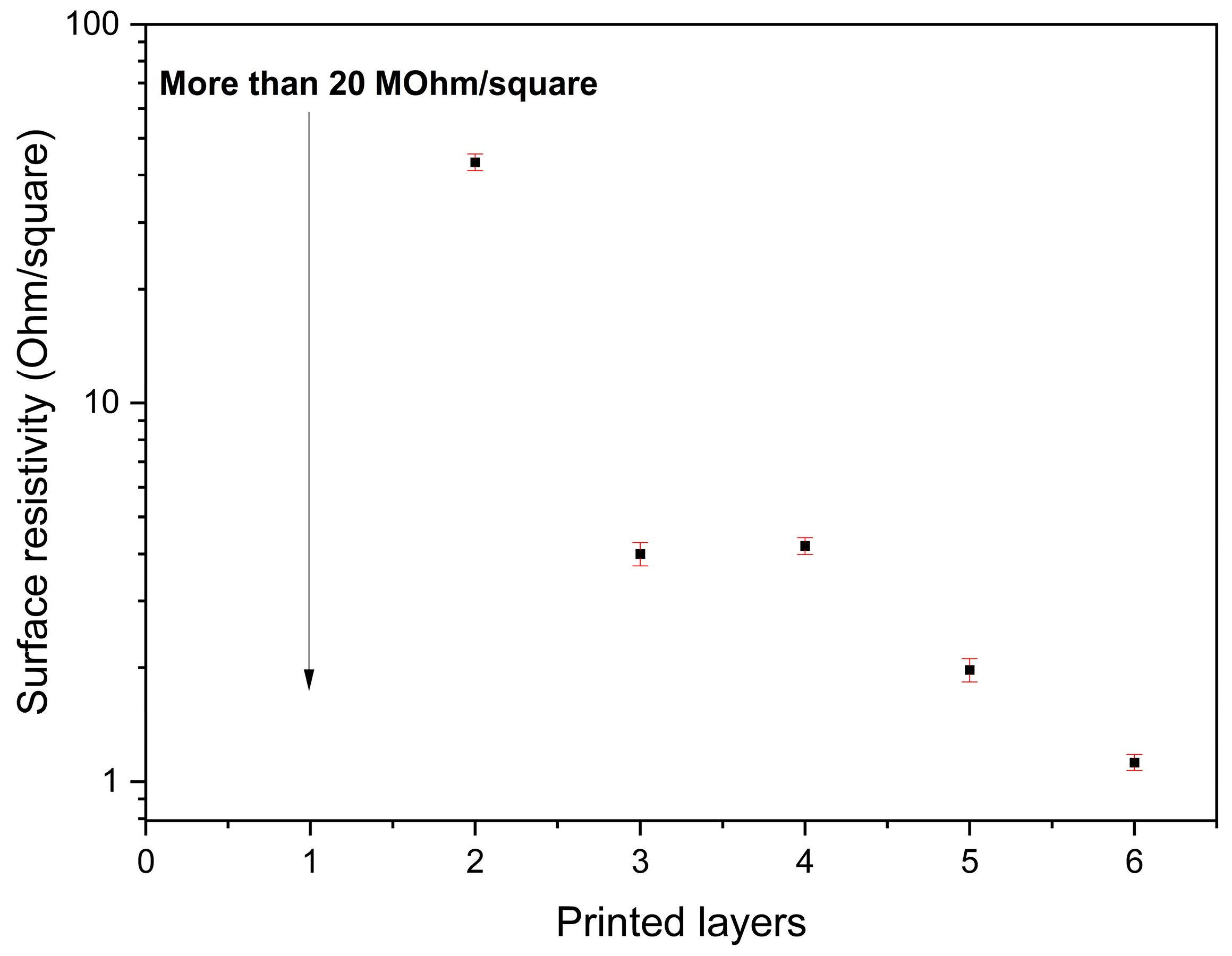
Due to its effectiveness regarding the electrical properties of the printed patterns, we decided to continue using electrospun PCL onto baking paper as printing substrate. Patterns with one to six printed layers were printed, transferred and cured and the electrical conductivity was measured. The results are shown in Figure 3.
The quantity of layers required to obtain a conductive track after curing process depends on the local concentration of the metallic nanoparticles and also on the characteristics of the substrate [18]. For porous substrates the ink was able to penetrate through the pores among the electrospun fibers leading to the occurrence of different resistivity levels due to the partial filling of the porous with the successive printed layers. Nonporous materials that present conductivity with only one printed layer have been reported and tested and no diffusion effect was noticed [20,21]. In this case, three different levels of resistivity were observed at 2, 3 and 5 printed layers.
Figure 3.
Surface resistivity of tracks with 1 to 6 printed layers after transfer and curing process using PCL onto baking paper as printing substrate.
Figure 3.
Surface resistivity of tracks with 1 to 6 printed layers after transfer and curing process using PCL onto baking paper as printing substrate.
3.2. Morphological Characterization of Transferred and Cured Tracks
Figure 4 shows the line width difference (WD) using different printing conditions and nominal line widths. WD was calculated according to the following equation:
where W_printed is the average line width calculated from 15 samples from each printed line and W_design is the nominal line width. The WD was calculated for tracks printed parallel and perpendicular to fiber’s orientation.
It could be noticed that the printed lines are wider than predicted by design. This is due to the porous nature of the substrate that produces some ink spreading. The difference in line width was easily noticeable, ranging from 150 to 700 microns, and increases with nominal width and number of printed layers as expected. The porous characteristics of the electrospun substrate also influence the line width difference since it was larger when lines were printed perpendicular to the fibers. However, the line widths were reproducible showing a maximum standard error of 22 microns. Regarding these results, it is possible to establish coherent design rules for printing conductive tracks onto electrospun PCL using silver nanoparticle inks. However, it is very important to carefully control the electrospinning process to obtain reproducible results with different batches of electrospun substrates.
Transfer and curing process were carried out at 80 °C and 145 °C respectively. During transfer process was noticeable a thermal contraction effect. Dimensional differences after curing process were measured for printed patterns with 500 µm width (by design) and showed in Table 2.
Shrinkage was observed for both senses (parallel and perpendicular to fiber’s orientation) but was larger perpendicular to the fibers as expected due to the pore morphology of the electrospun mat. Moreover, the shrinkage after curing was lower as the number of printed layers increased due to the presence of higher load of metallic nanoparticles inside the pores of the substrate.
SEM images of printed patterns with one to six printed layers before and after transfer and curing process were taken. Figure 5 compares the front and back sides of the printed PCL electrospun mat for one, three, five and six printed layers. The occurrence of ink diffusion process by concentration of most of ink on the back side could be observed (Figure 5e). This trend changed for three printed layers, showing both sides almost full of ink. Moreover, the saturation of the pores on the front side occured at six printed layers (Figure 5d).
These results confirmed the ink diffusion through the pores of of PCL electropsun fibers. The silver ink diffusion trough porous substrates were previously reported by other authors regarding printed electronics applications [19,20,21]. Intensity of the diffusion process depends on the porosity and the affinity of the ink to the substrate. This phenomenon also affects the quantity of printed layers needed to obtain an electrically conductive pattern after curing.
Ink buildup allows both sides of the electropun PCL mats to be conductive and, in turn, interconnect with each other, allowing different printed designs to be electrically connected by simply overlapping them, regardless of which is transferred first and without the need to be transferred at the same time.
Transfer and curing steps produce contraction and melting on the PCL electrospun fibers, as can be observed, especially in Figure 6a. Upon coming into contact with a piece at 80 °C, fibers melt and merge with neighbouring fibers, forming larger diameter fibers and, in turn, leaving voids on the surface. It is noteworthy that this effect decreased with increasing printed layers (Figure 8b-d). In addition, it was observed that the fibers within the ink layer did not show large structural changes after transfer at 80 °C. This phenomenon is due to the fact that the pores of the fibres are filled with silver ink, which prevents their agglomeration, maintaining a structure similar to that before the transfer.
In the case of cured fibers, thermal contraction was observed, especially in the mat with one printed layer, revealing inhomogeneities with voids of 17 µm on average. For the fibers with one layer, a rough film with holes was observed, where the fibrillar structure is completely lost. Thermal contraction was markedly lower for the fibres with three, five and six layers, where the fibrillar structure was maintained, although with the appearance of some voids. The SEM images are in accordance to the electrical resistance measurements (Figure 3) and track width measurements after curing (Table 2). Ink filling from three and more printed layers prevents the contraction of the printed tracks and provides a continuous path of sintered silver for electrical conduction.
Profilometry of printed tracks with two, three, four and six printed layers transferred and cured onto a PET film are shown in Figure 7.
Figure 7.
Thickness of printed patterns vs. printed layers after curing process.
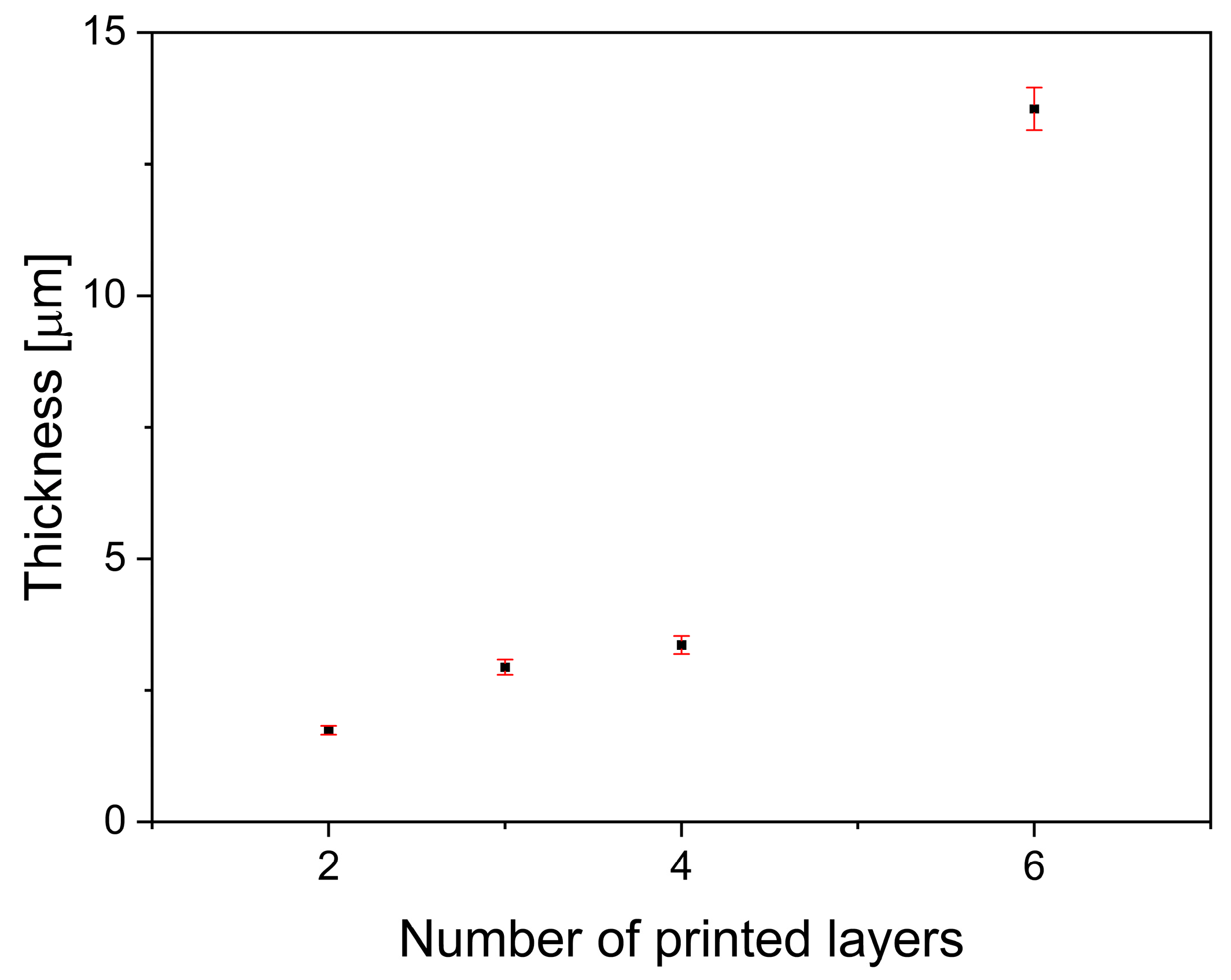
The printed tracks showed a larger thickness than the PCL electrospun mat. Two printed layer track was 1.74 μm thick whereas three and four layered tracks were 2.94 and 3.36 μm respectively. A large increase of the track thickness was observed for six printed layers (13.55 μm). This behaviour could be explained by the diffusion of the ink through the porous matrix until the saturation. Once the pores fully filed with ink, each layer led to a higher thickness after the curing process.
3.3. Rub Resistance
To evaluate adherence and mechanical properties of the printed tracks, a rub resistance test based on standard ISO 105-A01:2010-01 was performed on printed tracks with three, four and six printed layers. Printed patterns transferred to PLA 3D printed pieces and cured were assayed using the apparatus shown in Figure 8b. The rub cycles were performed perpendicular to the track. Electrical resistant measurements were performed after 10 cycles (each cycle includes 2 rub steps onto the transferred design). Results of electrical resistance after rub cycles were summarized in Figure 8a.
Figure 8.
Sheet resistivity after incremental rub stress cycles (a) and rub resistance apparatus (b).
Figure 8.
Sheet resistivity after incremental rub stress cycles (a) and rub resistance apparatus (b).
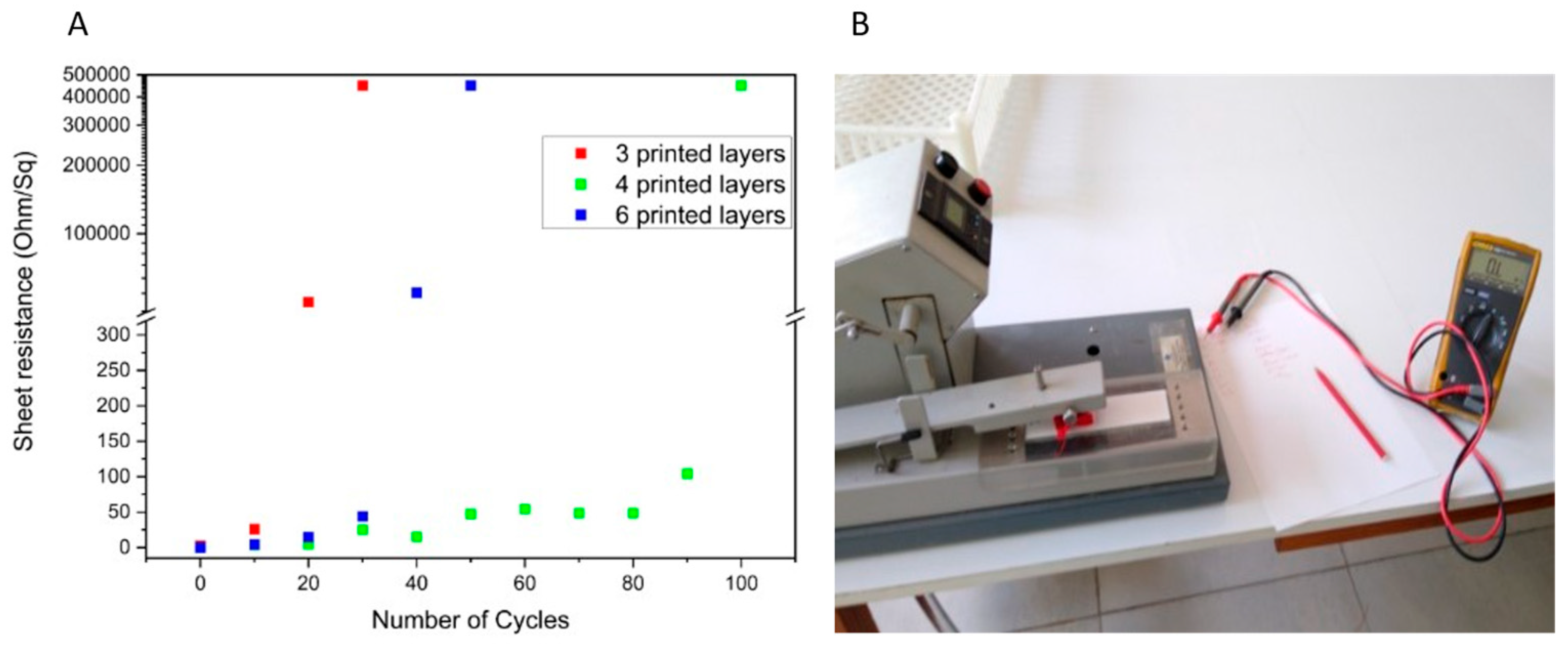
The samples with three layers underwent changes in their electrical resistance in the first 10 cycles, increasing the resistance by one order of magnitude while, after 20 cycles, the increase in electrical resistance was three orders of magnitude, losing all functionality after 30 cycles. The samples with four and six layers showed practically no change until after 20 cycles. After 30 cycles, an order of magnitude increase in resistance was observed in both samples. Samples with four layers remained close to that value until after 80 cycles and lost functionality after 100 while the samples with six layers began to lose functionality after 40 cycles with an increase of electrical resistance of four orders of magnitude and lost it completely after 50 cycles.
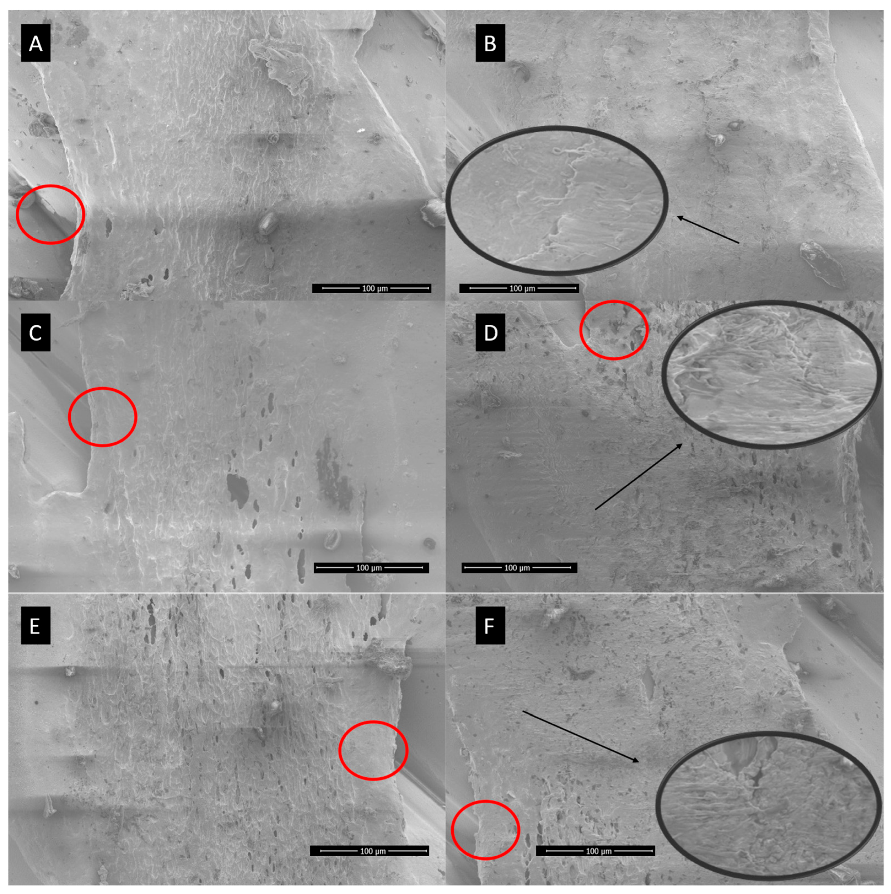
The rub resistance test shows that increasing the number of layers has consequences on mechanical properties and cohesion, as well as electrical conductivity. To understand this behavior regarding rubbing and the failure mechanism, SEM images of all the samples that were subjected to rubbing were taken and the images before and after failure were compared. Figure 9a shows shows images of the zone subjected to rubbing before and after the loss of functionality due to rubbing for the lines with three, four and six layers.
SEM images after rubbing (Figure 9) show that tracks were affected by rubbing. The printed silver layer has been dragged with the passes in every case. It was also observed that there is an influence of the printed the 3D printed layer in the rub resistance. This is because fused filament 3D printing is an additive technique that fuses filament lines one beside the other, inevitably leaving valleys and mountains along the surface. It is clearly observed that the fibers attached to a valley sector remained adhered to the 3D-printed surface, while those on a mountain were pulled out from the surface.
Figure 9.
SEM immages before and after the loss of functionality due to rubbing for the lines with three (a-b), four (c-d) and six layers (e-f).
Figure 9.
SEM immages before and after the loss of functionality due to rubbing for the lines with three (a-b), four (c-d) and six layers (e-f).
The results can be explained considering that the ink layers are sintered. By increasing the thickness of the layer, there is a higher concentration of particles and, therefore, a better initial conductivity. On the other hand, a thicker layer of sintered ink has greater resistance to rubbing. It is expected that the ink layer will remain cohesive against the shear stress that occurs during rubbing. First, the greater the number of layers, the larger the thickness of the cured pattern. Therefore, the resistance to the passage of the cloth increases with the number of layers, generating a greater shear stress, as exemplified in Figure 10. On the other hand, by increasing the number of printed layers, a saturation of the pores with ink was observed. The greater the saturation of the pores, the greater the mechanical resistance to shearing of the pattern, because it will have less chance of deformation as the cloth passes.
The first mechanism allows us to explain the differences between the samples with three and four layers and the one with six layers where a difference of 300% was observed in the thickness of the conductive silver track. On the other hand, the thickness of the deposit with three and four layers presented little variation among themselves. The tracks with six layers, although it presents a more solid structure due to having a greater filling of the pores, it has a much greater thickness that generates a larger shear stress during rubbing. Although there were no significant differences in thickness between the tracks with three and four layers, the track printed with four layers will have a higher saturation of silver particles within the fibres, and thus the accumulation of particles not only generates more of conductive channels, but also gives greater toughness to the mechanical assembly formed by the fibers and the neighboring sintered silver nanoparticles. This feature allowed the system with four layers to achieve a greater resistance to rubbing cycles.
3.4. Tracks Transferred to Non-Planar Surfaces and Flexible Acceptor Substrates
In order to demonstrate the application of the transfer to different topologies and receptor substrates, different printed patterns were printed and transferred to PLA 3D printed surfaces (planar, with concavities and sharp edges), flexible PET film and elastic TPU film as shown in Figure 11.
All the patterns showed electrical conductivity after curing process regardless of the topology and composition of the receptor substrate. Electrical conductivity of the tracks transferred to flexible substrates of PET and TPU were measured and mean values of 3 and 4 Ω/Square respectively and mantained their conductivity after bending.
The occurrence of ink diffusion process led to the presence of ink in both sides of the mat of fibers that allows the connection of two different printed tracks transferred separately. In order to prove this assumption different printed patterns were transferred partially overlapping one on top of the other and cured in separated steps as shown in Figure 10d. Their electrical surface resistivities were summarized in Table 3.
Electrical continuity was verified even after connecting patterns in different transfer and curing steps or by transferring a printed track from one side to the opposite of the 3d-printed piece passing by sharp 90 degrees edges. Thus, this system demonstrated to be modular and adaptable to different surface topologies. Modularity is a desiderably property in this kind of system due to the possibility of modifying, enlarging or repairing previously transferred and cured circuits.
3.5. Transference of an Interdigitated Electrode onto Nonplanar 3D Printed PLA Substrates
In order to determine the performance of the printing and transfer process, an interdigitated electrode with W/L = 220 was printed and transferred to a 3D printed surface with a concavity. Concavities printed using 3D printing process could lead to the occurrence of a rough surface. Problems with rough surfaces were also reported by other authors and solved by polishing the surface or by adding levelling layer with another material before the transfer process [18]. The surface of the concavity was polished to minimize the presence of the printed layer imperfections, minimizing the occurrence of defects on the fingers of the interdigitated electrode. The printing, transfer and curing process was shown in Figure 12.
The transferred interdigitated electrode was tested as a capacitive touch sensor to sense the presence of a finger in the cavity. The sensor showed an increasement of 22pF when a finger was pressed onto the sensor. Therefore, this transfer system is potentially attractive as an economic way of incorporating capacitive sensors or circuits into previously molded non-flat pieces (industry for the fabrication of touch buttons or LED lighting circuits).
4. Conclusions
A novel thermal transfer method of electrically conductive metallic silver patterns printed with inkjet printing onto mats of PCL fibers fabricated by electrospinning using nonplanar pieces as receptor substrate was developed. The printing substrate and the printing conditions were optimized in order to obtain an electrically conductive and reproducible printed pattern. It was found that baking paper could be used underneath the electrospun PCL mat in order to retain the silver nanoparticle ink within the pores of the electrospun mat, and at least two layers had to be printed in order to provide electrical conductivity. It was shown that the number of printed layers affected not only the final functionality but also the final mechanical stability of the design. On the other hand, the presence of a diffusive process of the ink through the pores of the fibers mat was observed. This ink diffusion led to tracks that were wider than predicted by design but reproducible. This process also rendered both sides of the PCL electrospun mat conductive, which in turn allowed the electrical connection of different printed patterns transferred separately. Moreover, the printed tracks could be transferred to nonplanar surfaces along sharp edges retaining electrical connection. These features allow the use of this transfer system for the creation of modular interconnection in complex nonplanar pieces.
The rub resistance of tracks cured with different number of printed layers was also evaluated, and it was found that the system was able to withstand the rubbing of a microfiber cloth and retain electrical continuity even after 160 passes. Such transfer system is presented as a potential alternative for application in topologies where conventional techniques such as inkjet printing or stamping show difficulties, for example, in fabrication of electronics as capacitive touch panels on molded parts with application in the automotive industry, among others.
Author Contributions
Conceptualization, F. N. Molinari and L. M. Monsalve; methodology, F. N. Molinari and E. Bilbao.; validation, F. N. Molinari and E. Bilbao; formal analysis, F. N. Molinari and L. N. Monsalve; investigation, F. N. Molinari, E. Bilbao and L. N. Monsalve; resources, L. N. Monsalve; data curation, F. N. Molinari, E. Bilbao and L. N. Monsalve; writing—original draft preparation, F. N. Molinari, E. Bilbao and L. N. Monsalve; writing—review and editing, F. N. Molinari, E. Bilbao and L. N. Monsalve; visualization, F. N. Molinari and L. N. Monsalve.; supervision, L. N. Monsalve; project administration, L. N. Monsalve; funding acquisition, L. N. Monsalve. All authors have read and agreed to the published version of the manuscript.
Funding
This research was funded by INTI, ANPCyT (PICT 2013-0427, PICT 2014-3748 and PICT 2017-2787) and CONICET (PIP 11220150100967).
Acknowledgments
We thank INTI, ANPCyT (PICT 2013-0427, PICT 2014-3748 and PICT 2017-2787) and CONICET (PIP 11220150100967) for financial support. LNM is research staff of CONICET. Authors are grateful to Theo Rodríguez Campos for the measurements of printed line widths.
Conflicts of Interest
The authors declare no conflicts of interest.
References
- Jian, J.R.; Kim, T.; Park, J.S.; Wang, J.; Kim, W.S. High performance 3D printed electronics using electroless plated copper. AIP Adv. 2017, 7. [Google Scholar] [CrossRef]
- Keranen, A.; Heikkinen, M.; Raappana, P.; Saaski, J. Method and Arrangement for providing electrical Connection to In-Mold-Electronics. US 2017/0215756A1, 2017. [Google Scholar]
- Jo, Y.; Kim, J.Y.; Jung, S.; Ahn, B.Y.; Lewis, J.A.; Choi, Y.; Jeong, S. 3D polymer objects with electronic components interconnected: Via conformally printed electrodes. Nanoscale 2017, 9, 14798–14803. [Google Scholar] [CrossRef] [PubMed]
- Chen, I.M.; Liu, Y.; Yu, X.; Everhart, W.; Park, J.; Wang, Y.; Pan, H. Aerosol printing and flash sintering of conformal conductors on 3D nonplanar surfaces. Manuf. Lett. 2022, 31, 119–123. [Google Scholar] [CrossRef]
- Lewis, J.A.; Ahn, B.Y. Three-dimensional printed electronics. Nature 2015, 518, 42–43. [Google Scholar] [CrossRef] [PubMed]
- Park, J.S.; Kim, T.; Kim, W.S. Conductive Cellulose Composites with Low Percolation Threshold for 3D Printed Electronics. Sci. Rep. 2017, 7, 1–10. [Google Scholar] [CrossRef] [PubMed]
- Sowade, E.; Polomoshnov, M.; Willert, A.; Baumann, R.R. Toward 3D-Printed Electronics: Inkjet-Printed Vertical Metal Wire Interconnects and Screen-Printed Batteries. Adv. Eng. Mater. 2019, 21. [Google Scholar] [CrossRef]
- Flowers, P.F.; Reyes, C.; Ye, S.; Kim, M.J.; Wiley, B.J. 3D printing electronic components and circuits with conductive thermoplastic filament. Addit. Manuf. 2017, 18, 156–163. [Google Scholar] [CrossRef]
- Yu, X.; Liu, Y.; Pham, H.; Sarkar, S.; Ludwig, B.; Chen, I.; Everhart, W.; Park, J.; Wang, Y.; Pan, H. Customizable Nonplanar Printing of Lithium-Ion Batteries. Adv. Mater. Technol. 2019, 4, 1900645. [Google Scholar] [CrossRef]
- Izumi, K.; Yoshida, Y.; Tokito, S. Soft blanket gravure printing technology for finely patterned conductive layers on three-dimensional or curved surfaces. Jpn. J. Appl. Phys. 2017, 56. [Google Scholar] [CrossRef]
- Bakr, M.; Su, Y.; Bossuyt, F.; Vanfleteren, J. Effect of overmolding process on the integrity of electronic circuits, 2019 22nd Eur. Microelectron. Packag. Conf. Exhib. EMPC 2019, 2019, 1–8. [Google Scholar] [CrossRef]
- Sundaram, S.; Kim, D.S.; Baldo, M.A.; Hayward, R.C.; Matusik, W. 3D-Printed Self-Folding Electronics. ACS Appl. Mater. Interfaces. 2017, 9, 32290–32298. [Google Scholar] [CrossRef] [PubMed]
- Wang, C.; Sim, K.; Chen, J.; Kim, H.; Rao, Z.; Li, Y.; Chen, W.; Song, J.; Verduzco, R.; Yu, C. Soft Ultrathin Electronics Innervated Adaptive Fully Soft Robots. Adv. Mater. 2018, 30, 1–9. [Google Scholar] [CrossRef] [PubMed]
- Miyamoto, A.; Lee, S.; Cooray, N.F.; Lee, S.; Mori, M.; Matsuhisa, N.; Jin, H.; Yoda, L.; Yokota, T.; Itoh, A.; Sekino, M.; Kawasaki, H.; Ebihara, T.; Amagai, M.; Someya, T. Inflammation-free, gas-permeable, lightweight, stretchable on-skin electronics with nanomeshes. Nat. Nanotechnol. 2017, 12, 907–913. [Google Scholar] [CrossRef] [PubMed]
- Molinari, F.N.; Barragán, E.; Bilbao, E.; Patrone, L.; Giménez, G.; Medrano, A.V.; Tolley, A.; Monsalve, L.N. An electrospun Polymer Composite with Fullerene-Multiwalled Carbon Nanotube Exohedral Complexes can act as Memory Device. Elsevier Ltd, 2020. [Google Scholar] [CrossRef]
- Molinari, F.; Medrano, A.V.; Bacigalupe, A.; Escobar, M.; Monsalve, L.N. Different dispersion states of MWCNT in aligned conductive electrospun PCL/MWCNT composites, Fullerenes, Nanotub. Carbon Nanostructures 2018, 26, 667–674. [Google Scholar] [CrossRef]
- Saniei, H.; Mousavi, S. Surface modification of PLA 3D-printed implants by electrospinning with enhanced bioactivity and cell affinity. Polymer 2020, 196, 122467. [Google Scholar] [CrossRef]
- Saada, G.; Layani, M.; Chernevousky, A.; Magdassi, S. Hydroprinting Conductive Patterns onto 3D Structures. Adv. Mater. Technol. 2017, 2, 1–6. [Google Scholar] [CrossRef]
- Han, L.; Andrady, A.; Guzan, K.; Ensor, D. Electrospun composite nanofibers for sensor applications. In MRS Online Proceedings Library (OPL); 2010; pp. 61–66. [Google Scholar] [CrossRef]
- Zhu, D.; Wu, M. Highly Conductive Nano-Silver Circuits by Inkjet Printing. J. Electron. Mater. 2018, 47, 5133–5147. [Google Scholar] [CrossRef]
- Joubert, T.H.; Bezuidenhout, P.H.; Chen, H.; Smith, S.; Land, K.J. Inkjet-printed Silver Tracks on Different Paper Substrates. In Materials Today: Proceedings; Elsevier Ltd, 2015; pp. 3891–3900. [Google Scholar] [CrossRef]
Figure 1.
Design of printed tracks for rub resistance (A) and electrical and dimensional characterization (B).
Figure 1.
Design of printed tracks for rub resistance (A) and electrical and dimensional characterization (B).
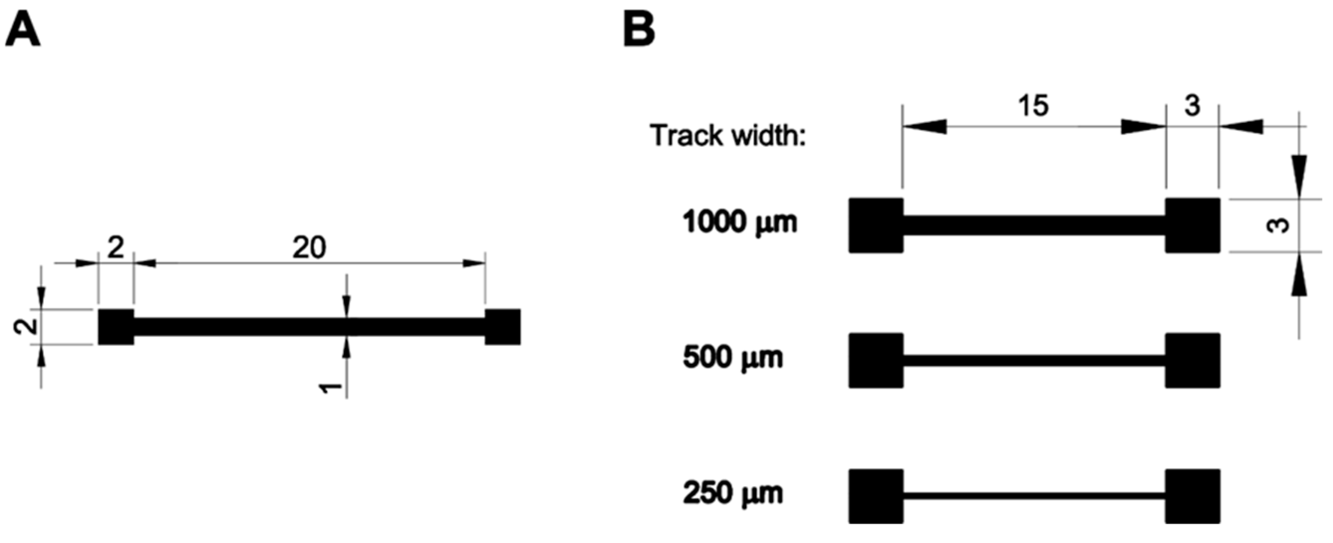
Figure 2.
Tracks with incremental printed layers on PCL onto kraft paper (A), baking paper (B) and sulphite paper (C) after the printing process.
Figure 2.
Tracks with incremental printed layers on PCL onto kraft paper (A), baking paper (B) and sulphite paper (C) after the printing process.
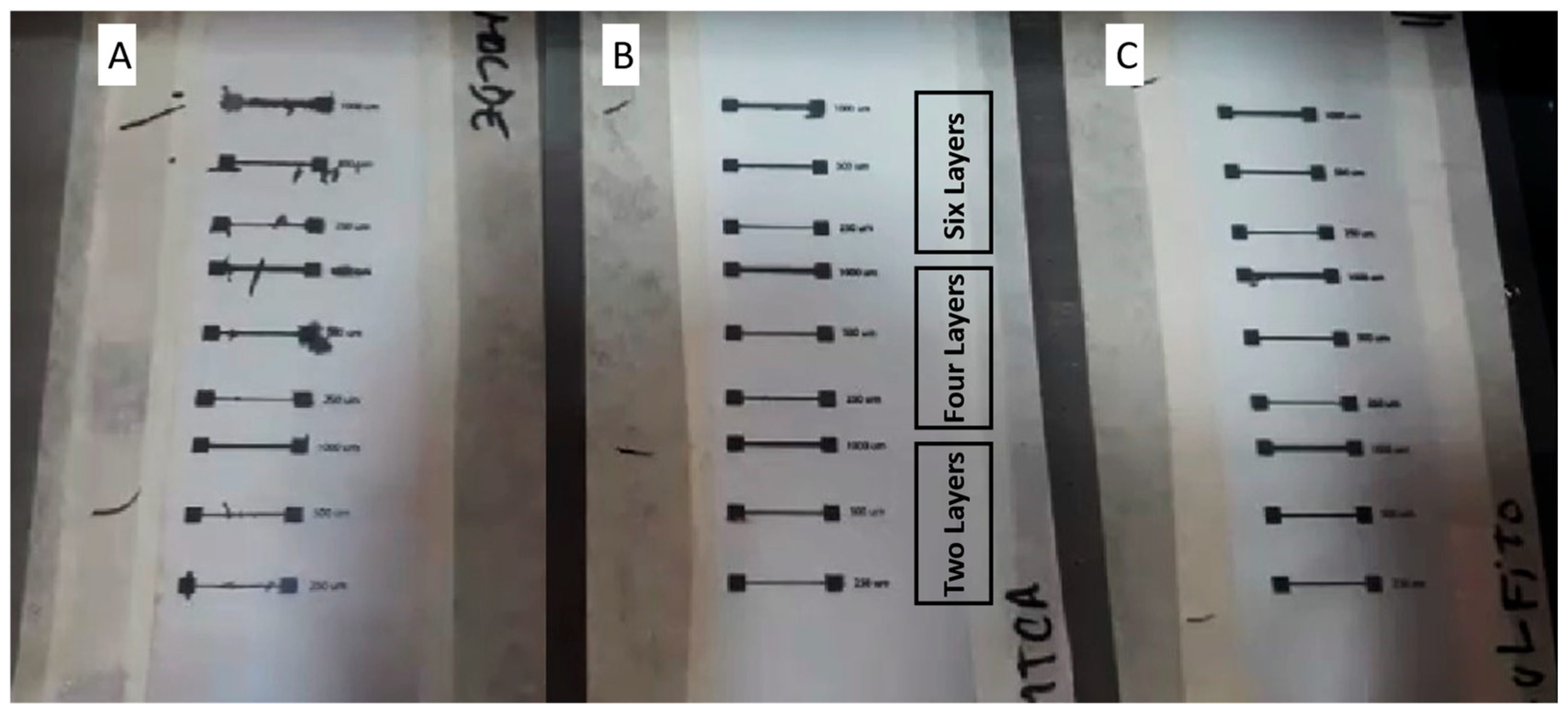
Figure 4.
Line width difference as function of nominal line width, number of layers and orientation to fiber fibers’ orientation. Lines were printed onto PCL mats onto baking paper.
Figure 4.
Line width difference as function of nominal line width, number of layers and orientation to fiber fibers’ orientation. Lines were printed onto PCL mats onto baking paper.
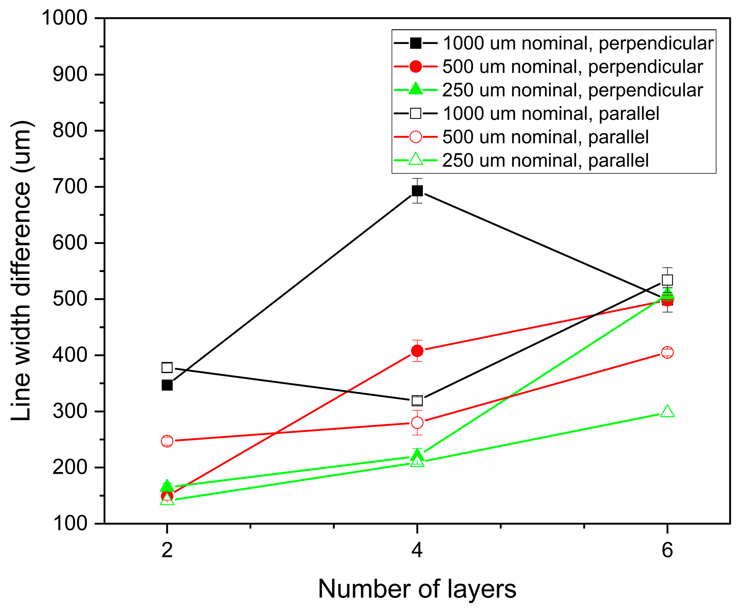
Figure 5.
SEM images of both sides of a printed mat of fibers with one (a, e), three (b, f), five (c, g) and six printed layers (e, h). Front side (Figures a-d) and back side (Figures e-h).
Figure 5.
SEM images of both sides of a printed mat of fibers with one (a, e), three (b, f), five (c, g) and six printed layers (e, h). Front side (Figures a-d) and back side (Figures e-h).
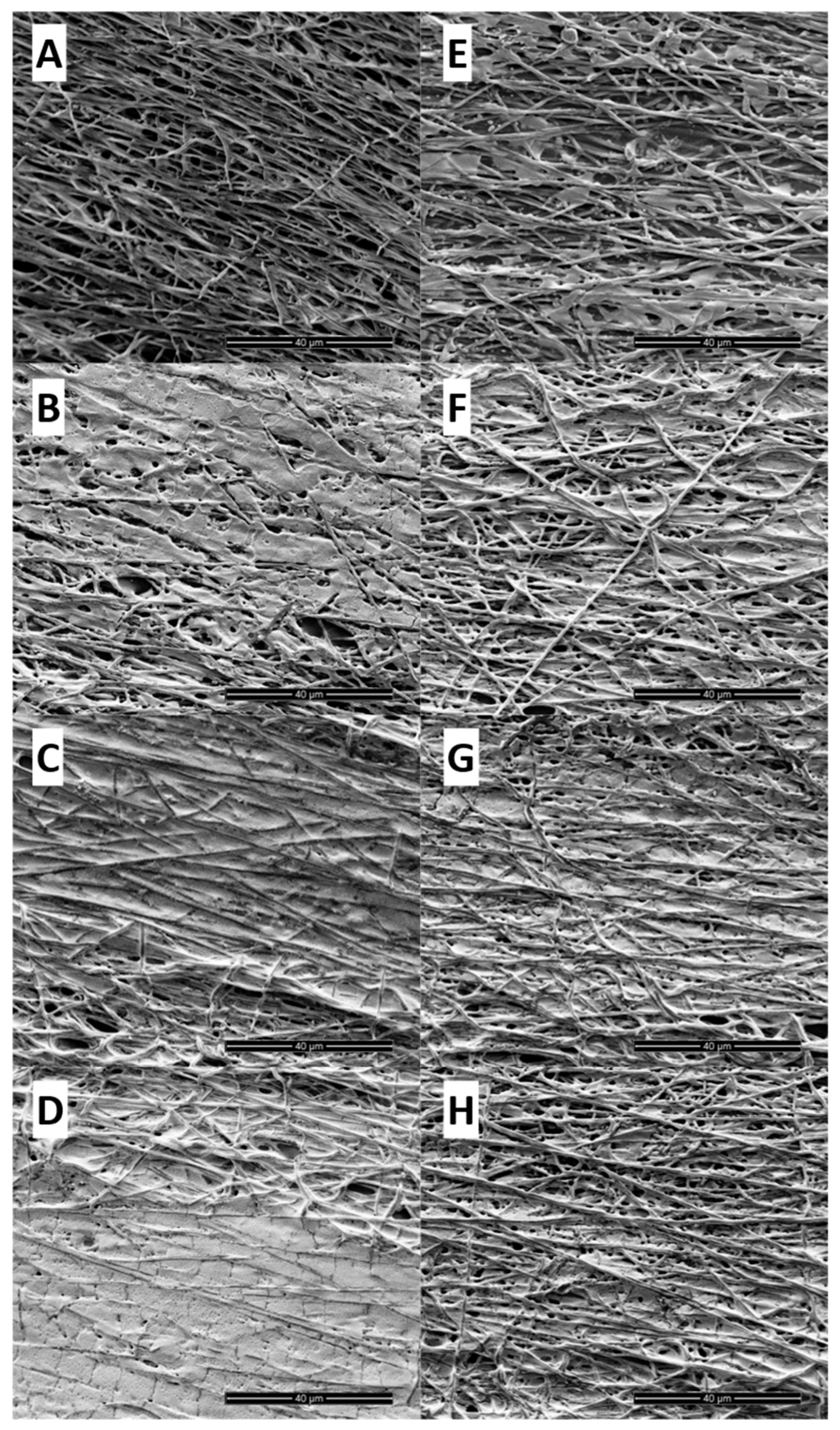
Figure 6.
SEM images of the front side of a printed mat of fibers with one (a), three (b), five (c) and six printed layers (d). After transfer step (Figures a-d) and after curing step (Figures e-h).
Figure 6.
SEM images of the front side of a printed mat of fibers with one (a), three (b), five (c) and six printed layers (d). After transfer step (Figures a-d) and after curing step (Figures e-h).
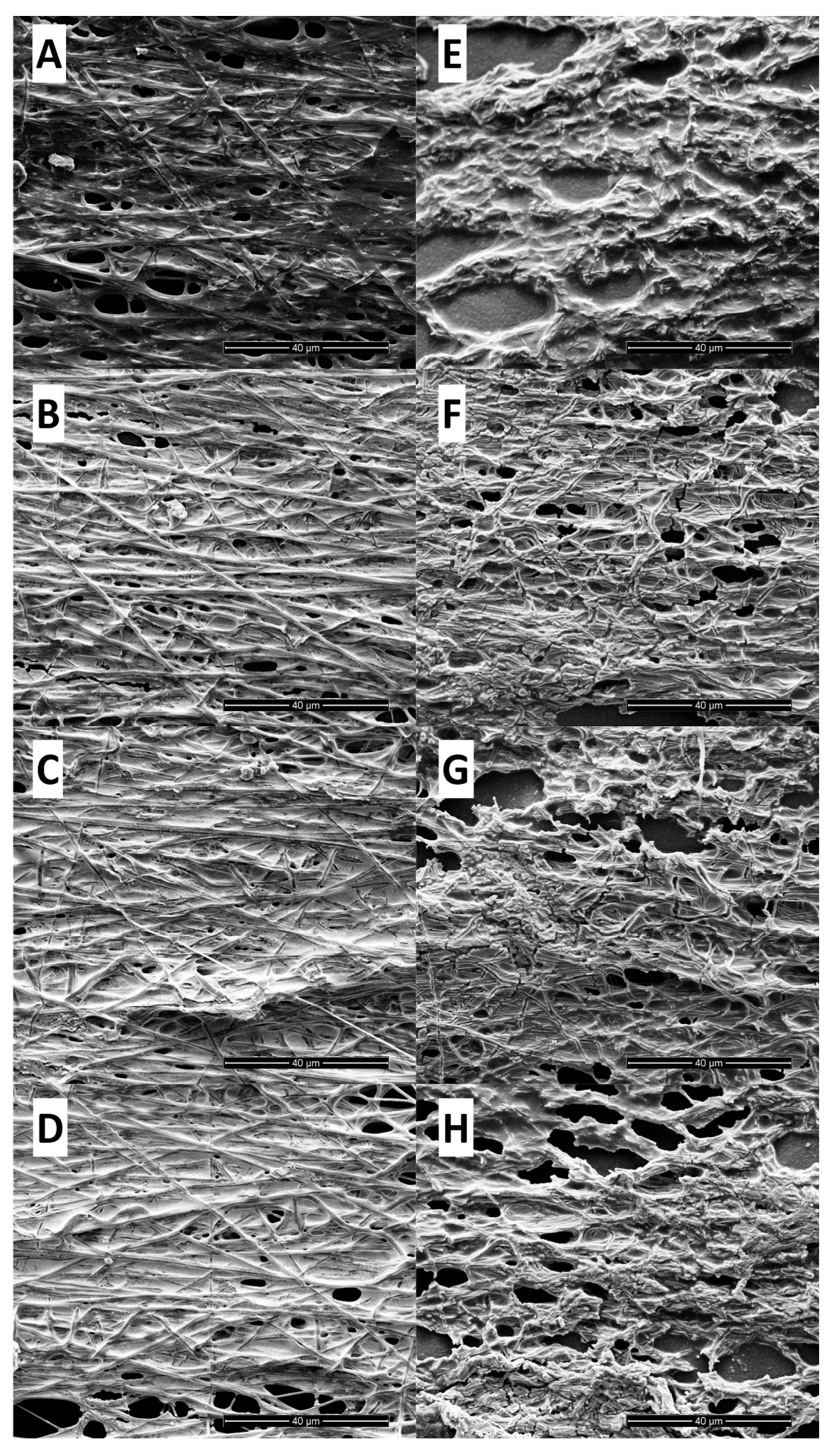
Figure 10.
Schema of the proposed mechanism of failure by rubbing.
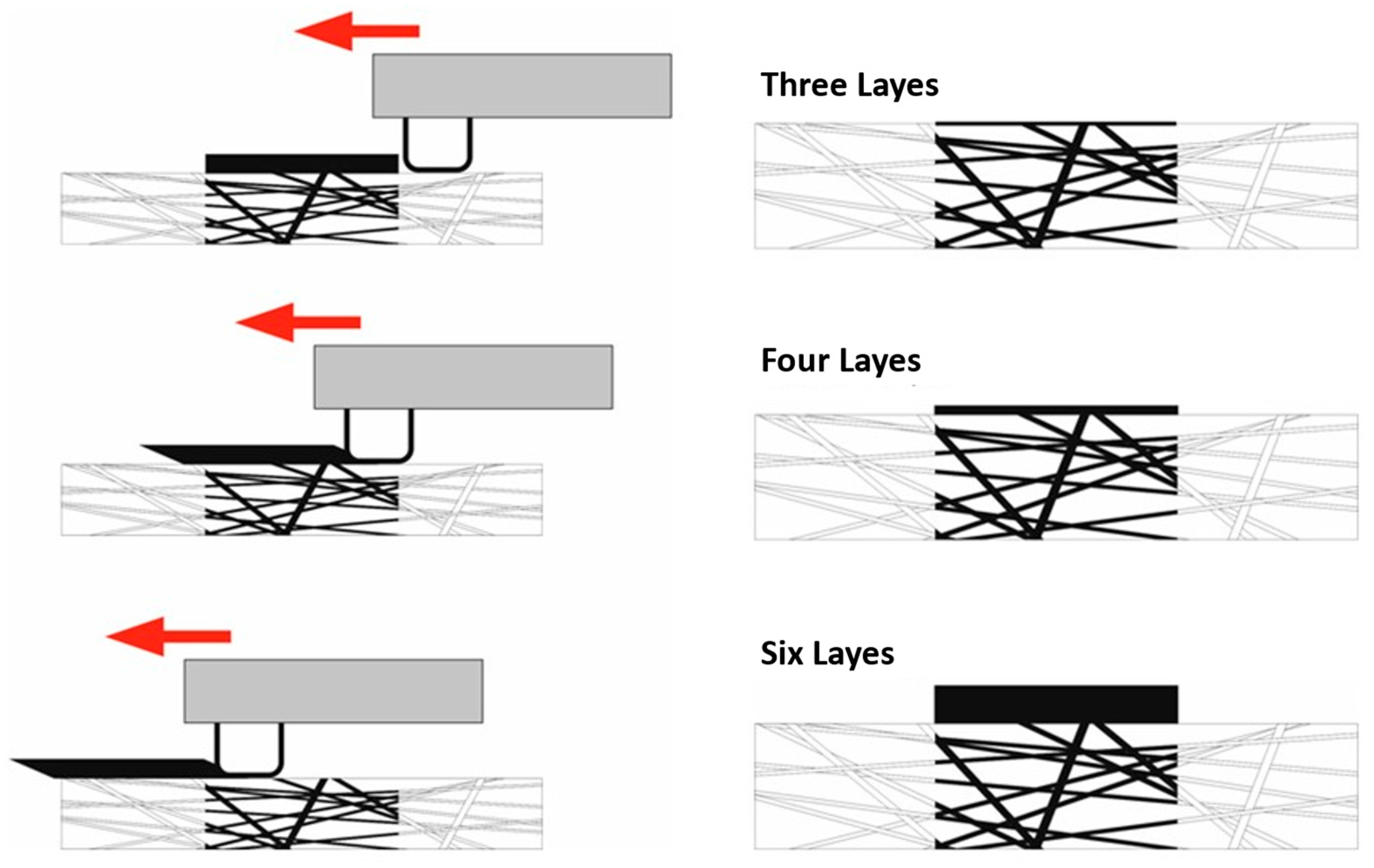
Figure 11.
Tracks with six printed layers transferred to flexible TPU substrate (a), PET substrate (b), non-planar 3D printed PLA substrate (c) and 90° angle 3D printed PLA substrate (d).
Figure 11.
Tracks with six printed layers transferred to flexible TPU substrate (a), PET substrate (b), non-planar 3D printed PLA substrate (c) and 90° angle 3D printed PLA substrate (d).
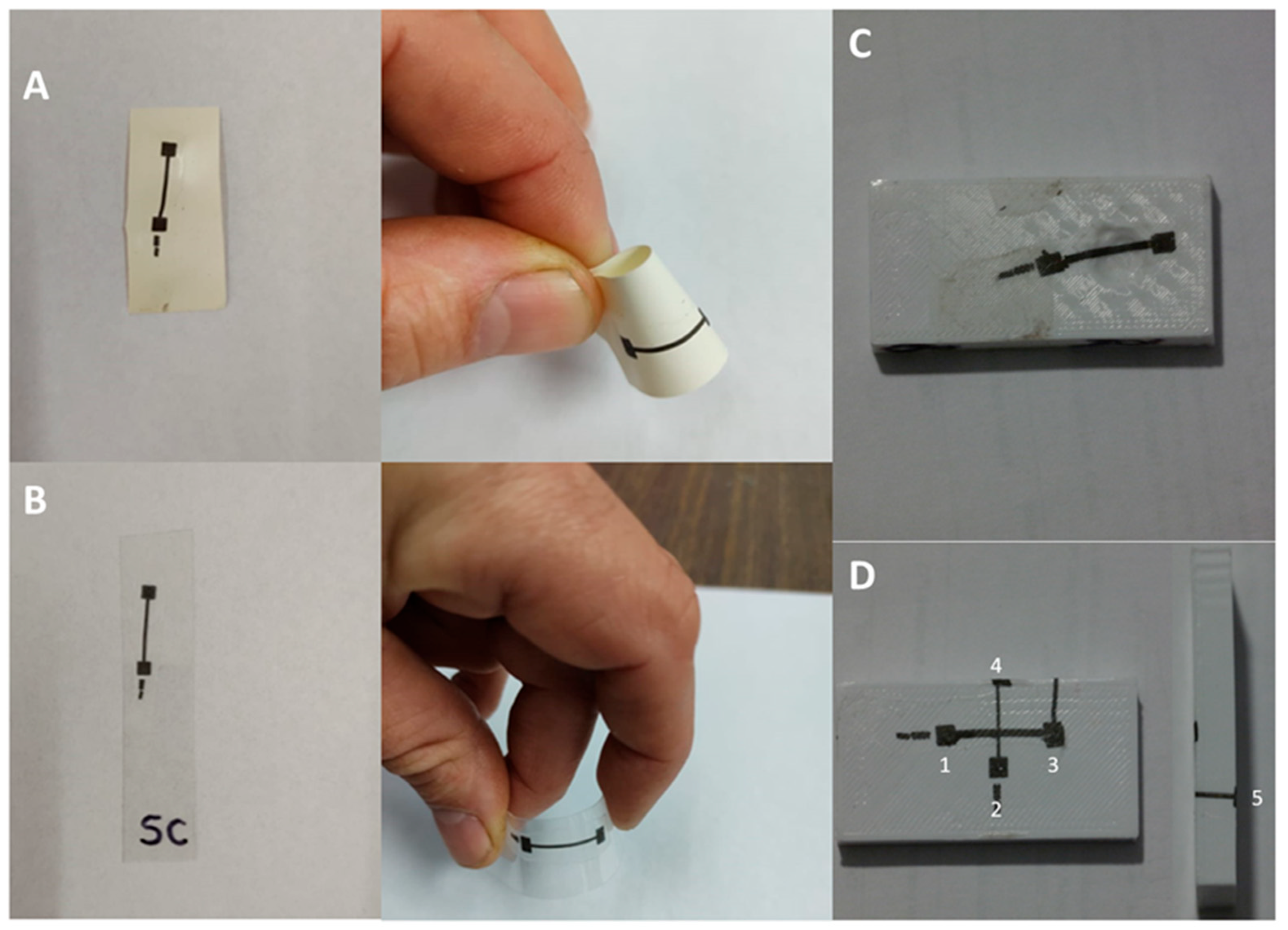
Figure 12.
Printing transfer and curing process of an interdigitated electrode onto a 3D printed PLA substrate with a cavity. a) As spun fibers onto baking paper and prepared to printing process. b-c) Electrodes printed onto the PCL fibers. d) 3D-printed piece with interdigitated electrode on a concave surface after transfer and curing process.
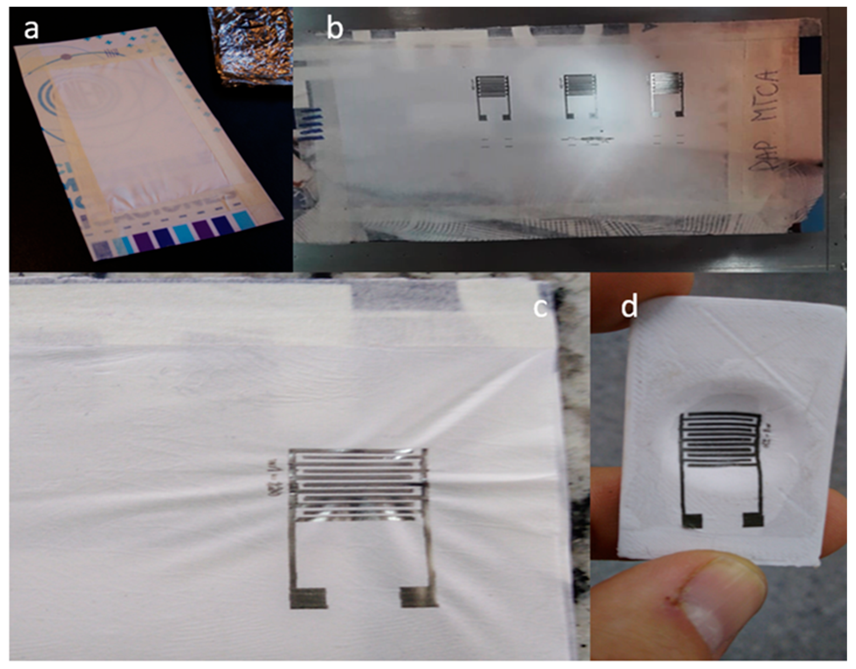

Table 1.
Surface resistivity of transferred and cured tracks with 2, 4 and 6 printed layers using different printing substrates.
Table 1.
Surface resistivity of transferred and cured tracks with 2, 4 and 6 printed layers using different printing substrates.
| Number of printed layers | 2 | 4 | 6 |
| Donor substrate | Surface resistivity [Ω/Square] | ||
| Kraft paper | - | - | - |
| Sulphite paper | - | - | - |
| Baking paper | 43.3 ± 2.5 | 4.2 ± 0.5 | 1.9 ± 0.2 |
Table 2.
Effect of thermal contraction of the tracks after transfer and curing process depending on the fiber orientation.
Table 2.
Effect of thermal contraction of the tracks after transfer and curing process depending on the fiber orientation.
| Number of printed layers | Difference ┴ [µm] | Difference // [µm] |
| 2 | -262 ± 5 | -52 ± 2 |
| 4 | -95 ± 7 | -27 ± 2 |
| 6 | -17 ± 5 | -10 ± 1 |
Table 3.
Summarized electrical properties of tracks transferred and cured separately (see Figure 10d for reference).
Table 3.
Summarized electrical properties of tracks transferred and cured separately (see Figure 10d for reference).
| Track | Sheet resistance [Ω/Square] |
| 2-4 | 2.0 ± 0.3 |
| 1-3 | 0.9 ± 0.1 |
| 2-1 | 1.7 ± 0.2 |
| 4-1 | 1.9 ± 0.3 |
| 2-3 | 2.0 ± 0.1 |
| 4-3 | 1.7 ± 0.2 |
| 3-5 | 1.1 ± 0.2 |
| 1-5 | 3.1 ± 0.3 |
| 2-5 | 5.7 ± 0.7 |
Disclaimer/Publisher’s Note: The statements, opinions and data contained in all publications are solely those of the individual author(s) and contributor(s) and not of MDPI and/or the editor(s). MDPI and/or the editor(s) disclaim responsibility for any injury to people or property resulting from any ideas, methods, instructions or products referred to in the content. |
© 2025 by the authors. Licensee MDPI, Basel, Switzerland. This article is an open access article distributed under the terms and conditions of the Creative Commons Attribution (CC BY) license (http://creativecommons.org/licenses/by/4.0/).
Copyright: This open access article is published under a Creative Commons CC BY 4.0 license, which permit the free download, distribution, and reuse, provided that the author and preprint are cited in any reuse.


