
Submitted:
01 April 2025
Posted:
01 April 2025
You are already at the latest version
Abstract
We explore quantum well laser diodes based on two material systems, classical AlGaAs, and a rather exotic GaAsBi, with lasing at around 800 nm and 1100 nm, respectively for applications in pulse oximetry. These spectral regions and material families were selected due to closely matched effective penetration depth into soft tissue. An improved design of the band structure of device active areas was tested on both material systems, yielding enhancement of the two main parameters, output power and threshold current. A maximum emission power of the AlGaAs laser diode was registered at 4.9 mW (I = 60 mA, λ = 801 nm). For the GaAsBi-based devices, the target emission of 1106 nm was measured at pulsed mode with a peak output power of 9.4 mW (I = 3 A). While the most optimized structure based on three GaAsBi quantum wells surrounded by parabolically graded AlGaAs barriers was capable of 130 mW of peak power (I = 2 A, λ = 1025 nm) and a more than tenfold decrease in threshold current to 250 mA, when compared to a classical rectangular quantum well active region.
Keywords:
GaAsBi
; QW with parabolic graded barriers
; Laser diode
1. Introduction
The ever-growing demand for monitoring systems of human vitals drives the improvement of the components of integrated sensor systems. One area of possible improvement is pulse oximetry. Traditionally, 660 nm red and 940 nm near-infrared (NIR) emitters are used for oximetry applications [1]. While such technology has been capable of achieving satisfactory results in transmission measurements (e.g., finger clips), the accuracy of measurements in reflectance mode is hindered by the difference in penetration depth of these wavelengths. It has been demonstrated that an improvement could be achieved by using two NIR laser diodes (LD) with similar emission wavelengths, resulting in a similar optical path length. Nonetheless, using nearby emission lines results in technological challenges [2]. This underscores the need for further research and development in the field. Another solution can be using two NIR wavelengths in the vicinity of 800 nm and 1100 nm that are far apart and have a similar penetration depth into soft tissue. AlGaAs quantum well (QW) laser diodes are the obvious candidate for the emission line of 800 nm, while the choice of emitters operating at 1100 nm is more complicated. The classical material for this wavelength region is InGaAs. However, structures with over 20% of In necessary for emission at 1100 nm are prone to relaxation and a formation of a dislocation grid due to the large lattice mismatch with GaAs substrates. GaAsBi QW-based structures can be used to overcome this issue in addition to having many attractive properties for applications in laser diode active media. First of all, the introduction of Bi into the lattice of GaAs induces a substantial band gap reduction of up to 88 meV/%Bi [3], meaning that a small amount of host As atoms have to be replaced to achieve a large red-shift without inducting much strain in the structure that could result in dislocations that limit the applicability in devices. Additionally, the increase of Bi content also increases the spin-orbit split-off (SO) energy (due to a major influence on the valance band). At a Bi content of 10.5% in GaAsBi, the SO becomes larger than the band gap energy; in this way, a major Auger non-radiative recombination path can be suppressed [4]. Finally, bismides possess temperature-insensitive emission energy paired with stable room-temperature operation of GaAsBi-based devices, making cooling less crucial [5,6]. The latter properties are significant for device applications that are supposed to work in various environmental conditions and maintain the same accuracy levels, making GaAsBi the perfect candidate for the application-focused 1100 nm emitters. The ability to achieve lasing at longer wavelengths was demonstrated by Wu et al., who achieved 1142 nm emission with a GaAsBi QW laser diode [7]. Even though GaAsBi-based laser diodes have been successfully produced by many groups [7,8,9,10,11,12], their wider application is limited by the defective crystalline structure of the alloy, which negatively affects the reproducibility, threshold current (Ith), and maximum power output of the devices. Some of these defects consist of BiGa antisites [13], Bi clustering, which was shown to be energetically favored Bi atom ordering [14], CuPtB type ordering is also noticed in bismides, resulting in optical anisotropy of the structures [15,16]. Furthermore, Gelczuk et al. reported electron trap levels in n-type GaAsBi, that are crucial for device performance [17]. Where two out of the six trap states are related to Bi, specifically a complex defect containing a BiGa antisite [13]. The other four trap levels were associated with the low-temperature GaAs, which were shown to be a prominent current leakage channel in GaAsBi LDs [18]. The major cause of these defects is the complicated growth of the alloy that is usually conducted at a stoichiometric As to Ga flux ratio and a low growth temperature that also doubles as a limiting factor for Bi incorporation, meaning that high Bi content is achieved at extremely low growth, resulting in large defect density [19,20,21]. Several strategies have been employed to improve the performance of GaAsBi lasers. Marko et al. reported a decreased threshold current by introducing Al into the barriers [10]. Our earlier works were focused on enhancing the emission characteristics of quantum sturctures based both on pure AlGaAs and on GaAsBi alloy containing high Bi by designing parabolically graded barriers [22,23].
In this work, we explore the opportunity of application of two laser diode families, namely, AlGaAs and GaAsBi, in pulse oximetry with a purpose to reach the target wavelengths of about 800 and 1100 nm. GaAsBi QW–based laser diodes were optimized for emission at around 1100 nm, while structures based on the classical material approach of AlGaAs QWs were produced for emission in the vicinity of 800 nm, providing a reference of laser diode performance. Structures with both of the investigated compounds were produced with parabolically graded barriers to increase the maximum output power and decrease the Ith.
2. Structure Modeling and Growth
Two material systems were utilized to produce the presented laser structures. The AlGaAs alloy was selected for the shorter target wavelength due to its straightforward and well-established growth. On the other hand, a quite exotic material system, GaAsBi, was employed for the longer wavelength spectral region. Additionally, two different designs of the active area band structure, rectangular and parabolically graded barriers (PGBs), were developed for both material systems to clarify the beneficial impact of the PGBs on the device performance parameters. The laser structures in this work are named according to their structure design, with the first letter representing the geometry (R – standard rectangular; P – parabolic) and the second two letters representing the material system (Bi – GaAsBi; Al – AlGaAs).
The structures were simulated using nextnano3 software, allowing for comprehensive full-band quantum mechanical modeling. A one-dimensional (1D) simulation was conducted along the growth direction (z-axis). The electronic band structure was calculated employing the 8×8 k·p method within the effective mass approximation framework [24]. Only the -point was considered the conduction band minimum, and the two valence band maxima, corresponding to the heavy hole (hh) and light hole (lh) states, were both included in the calculations. Additionally, excitonic effects and temperature-induced variations of the band gap were incorporated into the simulations. Due to the matched lattice constants of AlGaAs and GaAs, strain-related effects were omitted from the model. The simulation parameters for GaAsBi, band gap, SO, elastic constant, lattice constant, and band offset were obtained from the literature [25,26,27,28].
Figure 1 illustrates the calculated band edges of four active areas of the studied laser diodes. Figure 1a presents the gain region of structure RAl, which consisted of two 2 nm GaAs rectangular quantum wells separated by 10 nm AlGaAs barriers containing 15% Al encapsulated in a 30% Al spacer. The simulation shows a weak interaction between the two QWs due to the overlap of the two electronic wavefunctions, the hole states are not interacting with each other. Figure 1b shows the result of the calculation regarding PAl. The active region consists of a parabolic AlGaAs QW, the aluminum content varies from 30% down to 9%. the QW has a thickness of 25 nm. The modeling shows the presence of a level inside of the parabola with a wavefunction wider than the previous case. In Figure 1c the gain region of RBi consisting of three 6.8 nm GaAsBi QWs with 7 nm GaAs barriers.
Figure 1d shows the active area of PBi, it consists of three 10 nm GaAsBi QWs with 10 nm GaAs barriers enclosed in AlGaAs parabolic barrier with an Al content that varies in-between 30 and 0%. In this gain region, the QWs are confined and the wavefunctions are localized in the wells in correspondence with the hole wavefunctions.
The presented laser structures were grown using a solid-source “Veeco GenXplor R&D” MBE system on Si-doped ( cm-3) n-type double-side polished GaAs substrates (100). The temperature was recorded with a “kSpace Associates BandiT” band edge thermometry system working in transmission mode. A similar growth procedure was performed for the highly doped GaAs contact and AlGaAs cladding layers for all four LDs. A standard degassing procedure at °C for ~10 min was performed to remove the native oxide. All LD structures followed a similar design with highly ( cm-3) doped by Si and Be n+ and p+ GaAs layers grown to ensure an ohmic contact. The growth rates varied from 300 to 580 nm/h. Further, Al0.5Ga0.5As cladding layers doped to cm-3 were grown with a 650 to 1200 nm/h growth rate. The growth rates for both material systems were reduced to a range of 300 to 450 nm/h for the active regions of the devices to achieve high quality and precision of growth. Moreover, contrary to AlGaAs, the growth of GaAsBi active regions must be carried out under specific growth conditions. A growth interruption was made before starting the growth of the bismuth-containing QW layer. The interruption was necessary to decrease the substrate temperature to °C, reduce and stabilize the As flux to closely match that of Ga, and deposit a Bi wetting layer. The Bi pre-deposition is performed to avoid the delayed incorporation described by Ludewig et al [29]. The growth of GaAsBi layers was performed in Bi-rich conditions thus, the Bi incorporation was limited solely by the substrate temperature. A major difference in structure design was implemented for the laser structure RBi, which was grown with a 1000 nm thick AlAs sacrificial layer. This layer will be used in further processing and will enable the removal of substrate and transfer onto an integration platform. Detailed information on the parameters of the device active area is given in Table 1.
The parabolic design of the barriers is created using an analog grading technique, where the parabolic shape of the conduction band is achieved by gradually decreasing the Al content from 30% to 0% in the case of laser diode PBi and to 9% for the structure PAl. This leads to a relatively intricate growth protocol, where the PGB is segmented into steps of four monolayers each, and a gradual decrease in Al content is implemented; the growth times are progressively extended due to the lowered growth rate resulting from the reduction in Al flux.
3. Processing and Characterization
After MBE growth, the laser structures were cleaned in acetone and isopropyl alcohol baths at °C for 10 min each, followed by rinsing in deionized water and drying on a hotplate at °C for 10 min. Next, the AZ1518 photoresist was spin-coated at 4000 RPM for 30 s and baked at °C for 60 s. The pattern of the designed structure containing 4 to 5 µm bars was exposed through the mask under 75 mW/cm2 dose of UV illumination. The developing process was carried out in H2O : AZ351B = 4:1 solution. The mesas were etched using a phosphorus acid solution of H2O : H2O2 : H3PO4 = 10:1:1 for 3 min. stopping in AlGaAs:Si cladding layer. The photoresist was removed by rinsing the sample in acetone, isopropyl alcohol, and deionized water, followed by O2 plasma cleaning for 5 min. An additional processing step was necessary for the laser structure RBi, where an n+ GaAs layer is uncovered from the top side, to enable testing of the structure before transfer. The laser bars were mechanically cleaved to form the ~500 µm Farby-Perot resonator. The metallization of ohmic contacts was done using an electron beam (VST Model TFDS-870), depositing Ti (15 nm) – Au (180 nm) on the p-type and AuGe (140 nm) – Ni (25 nm) – Au (40 nm) on the n-type substrate or n+ GaAs layer in the case of structure RBi. The electrical pumping of laser diodes was achieved using two set-ups. A CW (continuous wave) Agilent U8002A single output DC power supply was used for AlGaAs lasers and output power–injection current curves were recorded using a Thorlabs PDA50B-EC - Ge switchable gain detector. Spectra of investigated AlGaAs-based devices were registered in CW mode by optical spectrum analyzer Q8341 (Advantest) with a wavelength resolution of 0.01 to 0.05 nm. All measurements were performed at room temperature (293 K). Before the experiment, all samples were mounted on gold-plated copper heat sinks, and a thermoelectric Peltier cooler was used for temperature stabilization. GaAsBi – based lasers were measured via pulsed electrical pumping produced with AVTECH (AVRZ-5W-B) high voltage pulse generator operating at 1 kHz repetition rate with a pulse duration of 50 ns. A digital handheld optical power meter (Thorlabs PM100D) was used to register the output power. The lasing spectrum was dispersed through a 0.42 m monochromator (SPM-2) and detected with thermoelectrically cooled InGaAs photodetector (IGA-030-TE2-H). Current-voltage (I-V) characteristics under CW operation were measured using the precision source measure unit B2901 (Keysight) with a voltage step of 10 mV. The maximum permissible DC current and forward voltage was limited to avoid damage to the quantum well region.
4. Results Discussion
4.1. I-V Characteristics
The I-V characteristics of investigated laser diodes are typical for pn junction devices and can be expressed as , where I0 is the saturation current of a diode, q – an elementary charge, Rs – a series resistance of the diode, n – a non-ideality factor of the diode and k – a Boltzmann constant. The non-ideality factor varies in the range from 2 to 2.5 in the laser diodes presented in Figure 2 for the current interval of 10-7 to 10-5 A. Usually, a factor close to 2 shows a dominant generation-recombination current component in a p-n junction [30]. The current deviation from the exponential law at currents above 1 mA can be explained by the voltage drop on LD series resistance.
Here, the laser diode PAl is distinguished by a higher non-ideality factor in the low-current range below 10-8 A, which is attributed to the leakage current component. This usually indicates a slightly lower quality of the device/structure due to higher defectiveness, not necessarily related to the quantum well region of the LD. The subsequent measurements of optical characteristics confirm this: no negative effect on LD performance above the threshold was observed at this stage of characterization. However, during the operation, this leakage current can contribute to reduced LD reliability and influence the shorter lifetime of the device [31,32].
4.2. Light Output Characteristics
Figure 3 presents the injection current – output power characteristics measured for the two AlGaAs-based lasers, containing the standard rectangular design of the two QWs Figure 3a, and a single parabolic QW design Figure 3b. The lasing spectra of the diodes PAl and RAl are shown in the insets of Figure 3a,b. The two lasers have a similar emission line at 801 and 780 nm, respectively. These values well match the transition energy obtained by the nextnano3 modeling. The main lasing mode is mirrored by satellite Farby-Perot modes that are usual for as-cleaved laser diodes. The output power versus injection current characteristics reveal some inherent differences in the behavior of the two structures when a CW electrical current is applied. Even though the maximum output power measured for both diodes was similar, when comparing powers at the same injection current (60 mA) the laser PAl (Figure 3b) had a higher output at 4.9 mW compared to 3.2 mW for laser RAl (Figure 3a). Furthermore, a decrease in threshold current (Ith) from 43 mA for LD RAl to 35 mA for LD PAl is observed. Finally, a gradual loss in the linearity of the dependence for laser RAl becomes noticeable at around 55 mA of injection current, showing power saturation. Such results are rather unusual since the longer wavelength laser demonstrates better parameters. We propose that PGBs in the LD PAl are the reason for the enhanced device properties. Even though the nextnano3 simulation and the I-V characteristics would suggest that the design, confinment and quality of the laser PAl are less optimal the enhanced carrier capture efficiency by PGBs proposed by Pūkiene et al. has a more significant effect on the laser performance [22].
A CW operation of GaAsBi-based laser diodes could not be achieved due to problems related to defect formation promoted by the low-temperature growth and narrow window of As and Ga flux ratios that were discussed earlier. The peak output-power versus injection current plots and lasing spectra obtained under pulsed excitation (50 ns at 1 kHz) are depicted in Figure 4 and will be discussed separately. Lasing from the two diodes was recorded at a central wavelength of 1106 nm for LD RBi and 1024 nm for LD PBi. The red-shifted lasing wavelength of laser RBi is attributed to the higher Bi content in the GaAsBi QWs, which is estimated to be at ~7% and ~5% for structures RBi and PBi, respectively. The trend of enhanced laser parameters employing PGBs is maintained for GaAsBi-based emitters. The maximum output power was doubled from ~10 mW to ~20 mW at 3 A of injection current, in addition to a twofold decrease in Ith (2.5 A and 1.3 A) for the sample with the improved barrier design. Moreover, a laser diode with a thinned substrate was fabricated (Figure 4b black curve) and a drastic improvement was noticed. The peak pulse output power was increased by almost an order of magnitude to more than 130 mW and a further decrease in Ith was noticed, achieving values as low as 250 mA. Such significant effect of substrate thinning can be explained by two factors. First, the crystalline quality of the substrates is substantially worse than that of epitaxially grown layers, thus the larger defect density results in loss of carriers in the substrate, resulting in less of them reaching the active region. Second, the high defectiveness of bismides results in high resistance and significant local heating of the structure. The substrate thinning greatly enhances the temperature exhaust capabilities.
5. Conclusions
Application-focused QW LDs were fabricated for use in advancing the accuracy of pulse oximeters. LDs emitting in the range from 780 – 800 nm were produced using an AlGaAs material system. A maximum lasing output power of 4.9 mW was registered in the CW regime for the laser with PGBs emitting at 801 nm (Figure 3b), while the 782 nm laser with a classical rectangular design achieved 3.2 mW at the same injection (Figure 3a). GaAsBi alloy-based QW emitters exhibited lasing at the pulsed regime. A maximum peak output power of ~10 mW was recorded at a target wavelength of 1106 nm, where a classical rectangular design was used (Figure 4a). For a laser diode with three rectangular QWs embedded in PGBs, the recorded peak output power was 20 mW at 1025 nm (Figure 4b). The hypothesis that the improvement in carrier trapping efficiency would enhance the LD performance was confirmed. Both material systems showed improvement in output power and lasing threshold. While the improvement of the AlGaAs samples was not as pronounced as for the GaAsBi ones, where both parameters were improved twofold. The reduced impact on the properties of AlGaAs-based LDs is explained by the simulation (Figure 1b) and the I-V curves (Figure 2), hinting at a suboptimal quality and design of the laser PAl. Additional steps were carried out to investigate the impact on substrate thinning for the optimized GaAsBi-based LD PBi. A decrease in the threshold current of over 5 times in magnitude and more than 6 times increased output power was recorded with 250 mA of threshold current and over 130 mW of peak power produced by a GaAsBi-based LD at pulsed mode of operation.
Author Contributions
Conceptualization, R.B and J.Y.Ch.; methodology, A.Š., A.Z., A.B., J.G., M.K.; software, A.Z., B.Č.; validation, J.G., B.Č., A.B.; formal analysis, A.Š., A.Z., J.G., S.P., J.M., R.B.; investigation, A.Š., A.Z., A.B., J.G., M.K., S.P., V.B.; resources, R.B.; data curation, A.Š., A.Z., A.B., J.G.; writing—original draft preparation, A.Š, A.Z., R.B., J.S., J.Y.Ch.; writing—review and editing, A.Š, A.Z., R.B., J.S., J.Y.Ch.; visualization, A.Š., A.Z., J.G.; supervision, R.B.; project administration, R.B., J.S., Y.J.Ch; funding acquisition, R.B. All authors have read and agreed to the published version of the manuscript.
Funding
This research was funded by Research Council of Lithuania grant number S-LLT-23-3.
Data Availability Statement
The raw data supporting the conclusions of this article will be made available by the authors on request.
Conflicts of Interest
The authors declare no conflicts of interest.
References
- Sinex, J.E. Pulse oximetry: principles and limitations. Am. J. Emerg. Med. 1999, 17, 59–67. [Google Scholar] [CrossRef] [PubMed]
- Yossef Hay, O.; Cohen, M.; Nitzan, I.; Kasirer, Y.; Shahroor-Karni, S.; Yitzhaky, Y.; Engelberg, S.; Nitzan, M. Pulse oximetry with two infrared wavelengths without calibration in extracted arterial blood. Sensors (Basel) 2018, 18, 3457. [Google Scholar] [CrossRef] [PubMed]
- Francoeur, S.; Seong, M.J.; Mascarenhas, A.; Tixier, S.; Adamcyk, M.; Tiedje, T. Band gap of GaAs1-xBix, 0<x<3.6%. Appl. Phys. Lett. 2003, 82, 3874–3876. [Google Scholar] [CrossRef]
- Alberi, K.; Dubon, O.D.; Walukiewicz, W.; Yu, K.M.; Bertulis, K.; Krotkus, A. Valence band anticrossing in GaAs1-xBix. Appl. Phys. Lett. 2007, 91, 051909. [Google Scholar] [CrossRef]
- Oe, K.; Okamoto, H. New semiconductor alloy GaAs1-xBix grown by metal organic vapor phase epitaxy. Jpn. J. Appl. Phys. (2008) 1998, 37, L1283. [Google Scholar] [CrossRef]
- Tominaga, Y.; Oe, K.; Yoshimoto, M. Low temperature dependence of oscillation wavelength in GaAs1-xBix Laser by photo-pumping. Appl. Phys. Express 2010, 3, 062201. [Google Scholar] [CrossRef]
- Wu, X.; Pan, W.; Zhang, Z.; Li, Y.; Cao, C.; Liu, J.; Zhang, L.; Song, Y.; Ou, H.; Wang, S. 1.142 μm GaAsBi/GaAs quantum well lasers grown by molecular beam epitaxy. ACS Photonics 2017, 4, 1322–1326. [Google Scholar] [CrossRef]
- Ludewig, P.; Knaub, N.; Hossain, N.; Reinhard, S.; Nattermann, L.; Marko, I.P.; Jin, S.R.; Hild, K.; Chatterjee, S.; Stolz, W.; et al. Electrical injection Ga(AsBi)/(AlGa)As single quantum well laser. Appl. Phys. Lett. 2013, 102, 242115. [Google Scholar] [CrossRef]
- Butkutė, R.; Geižutis, A.; Pačebutas, V.; Čechavičius, B.; Bukauskas, V.; Kundrotas, R.; Ludewig, P.; Volz, K.; Krotkus, A. Multi-quantum well Ga(AsBi)/GaAs laser diodes with more than 6% of bismuth. Electron. Lett. 2014, 50, 1155–1157. [Google Scholar] [CrossRef]
- Marko, I.P.; Ludewig, P.; Bushell, Z.L.; Jin, S.R.; Hild, K.; Batool, Z.; Reinhard, S.; Nattermann, L.; Stolz, W.; Volz, K.; et al. Physical properties and optimization of GaBiAs/(Al)GaAs based near-infrared laser diodes grown by MOVPE with up to 4.4% Bi. J. Phys. D Appl. Phys. 2014, 47, 345103. [Google Scholar] [CrossRef]
- Fuyuki, T.; Yoshida, K.; Yoshioka, R.; Yoshimoto, M. Electrically pumped room-temperature operation of GaAs1-xBix laser diodes with low-temperature dependence of oscillation wavelength. Appl. Phys. Express 2014, 7, 082101. [Google Scholar] [CrossRef]
- Armalytė, S.; Glemža, J.; Jonkus, V.; Pralgauskaitė, S.; Matukas, J.; Pūkienė, S.; Zelioli, A.; Dudutienė, E.; Naujokaitis, A.; Bičiūnas, A.; et al. Low-frequency noise characteristics of (Al, Ga)As and Ga(As, Bi) quantum well structures for NIR laser diodes. Sensors (Basel) 2023, 23. [Google Scholar] [CrossRef] [PubMed]
- Luna, E.; Puustinen, J.; Hilska, J.; Guina, M. Detection of BiGa hetero-antisites at Ga(As,Bi)/(Al,Ga)As interfaces. J. Appl. Phys. 2024, 135. [Google Scholar] [CrossRef]
- Beyer, A.; Knaub, N.; Rosenow, P.; Jandieri, K.; Ludewig, P.; Bannow, L.; Koch, S.W.; Tonner, R.; Volz, K. Local Bi ordering in MOVPE grown Ga(As,Bi) investigated by high resolution scanning transmission electron microscopy. Appl. Mater. Today 2017, 6, 22–28. [Google Scholar] [CrossRef]
- Paulauskas, T.; Čechavičius, B.; Karpus, V.; Jočionis, L.; Tumėnas, S.; Devenson, J.; Pačebutas, V.; Stanionytė, S.; Strazdienė, V.; Geižutis, A.; et al. Polarization dependent photoluminescence and optical anisotropy in CuPtB-ordered dilute GaAs1-xBix alloys. J. Appl. Phys. 2020, 128, 195106. [Google Scholar] [CrossRef]
- Karpus, V.; Čechavičius, B.; Tumėnas, S.; Stanionytė, S.; Butkutė, R.; Skapas, M.; Paulauskas, T. Optical anisotropy of CuPt-ordered GaAsBi alloys. J. Phys. D Appl. Phys. 2021, 54, 504001. [Google Scholar] [CrossRef]
- Gelczuk, Ł.; Kopaczek, J.; Rockett, T.B.O.; Richards, R.D.; Kudrawiec, R. Deep-level defects in n-type GaAsBi alloys grown by molecular beam epitaxy at low temperature and their influence on optical properties. Sci. Rep. 2017, 7, 12824. [Google Scholar] [CrossRef]
- Glemža, J.; Špokas, A.; Zelioli, A.; Kamarauskas, M.; Bičiūnas, A.; Čechavičius, B.; Spigulis, J.; Chiu, Y.J.; Pralgauskaitė, S.; Matukas, J.; et al. Quality evaluation of NIR laser diodes for medical application using low-frequency noise characterization. Infrared Phys. Technol. 2025, 147, 105794. [Google Scholar] [CrossRef]
- Puustinen, J.; Hilska, J.; Guina, M. Analysis of GaAsBi growth regimes in high resolution with respect to As/Ga ratio using stationary MBE growth. J. Cryst. Growth 2019, 511, 33–41. [Google Scholar] [CrossRef]
- Richards, R.D.; Bastiman, F.; Hunter, C.J.; Mendes, D.F.; Mohmad, A.R.; Roberts, J.S.; David, J.P.R. Molecular beam epitaxy growth of GaAsBi using As2 and As4. J. Cryst. Growth 2014, 390, 120–124. [Google Scholar] [CrossRef]
- Rockett, T.B.O.; Richards, R.D.; Gu, Y.; Harun, F.; Liu, Y.; Zhou, Z.; David, J.P.R. Influence of growth conditions on the structural and opto-electronic quality of GaAsBi. J. Cryst. Growth 2017, 477, 139–143. [Google Scholar] [CrossRef]
- Pūkienė, S.; Karaliūnas, M.; Jasinskas, A.; Dudutienė, E.; Čechavičius, B.; Devenson, J.; Butkutė, R.; Udal, A.; Valušis, G. Enhancement of photoluminescence of GaAsBi quantum wells by parabolic design of AlGaAs barriers. Nanotechnology 2019, 30, 455001. [Google Scholar] [CrossRef]
- Karaliūnas, M.; Dudutienė, E.; Čerškus, A.; Pagalys, J.; Pūkienė, S.; Udal, A.; Butkutė, R.; Valušis, G. High precision parabolic quantum wells grown using pulsed analog alloy grading technique: Photoluminescence probing and fractional-dimensional space approach. Journal of Luminescence 2021, 239, 118321. [Google Scholar] [CrossRef]
- Andreani, L.C.; Pasquarello, A.; Bassani, F. Hole subbands in strained GaAs - Ga1-xAlxAs quantum wells: Exact solution of the effective-mass equation. Phys. Rev. B Condens. Matter 1987, 36, 5887–5894. [Google Scholar] [CrossRef] [PubMed]
- Mahtab, M.; Synowicki, R.; Bahrami-Yekta, V.; Bannow, L.C.; Koch, S.W.; Lewis, R.B.; Tiedje, T. Complex dielectric function of GaAs1-xBix as a function of Bi content. Phys. Rev. Mater. 2019, 3. [Google Scholar] [CrossRef]
- Ferhat, M.; Zaoui, A. Structural and electronic properties of III-V bismuth compounds. Phys. Rev. B Condens. Matter Mater. Phys. 2006, 73. [Google Scholar] [CrossRef]
- Janotti, A.; Wei, S.H.; Zhang, S.B. Theoretical study of the effects of isovalent coalloying of Bi and N in GaAs. Phys. Rev. B Condens. Matter 2002, 65. [Google Scholar] [CrossRef]
- Karpus, V.; Norkus, R.; Butkutė, R.; Stanionytė, S.; Čechavičius, B.; Krotkus, A. THz-excitation spectroscopy technique for band-offset determination. Opt. Express 2018, 26, 33807–33817. [Google Scholar] [CrossRef]
- Ludewig, P.; Knaub, N.; Stolz, W.; Volz, K. MOVPE growth of Ga(AsBi)/GaAs multi quantum well structures. J. Cryst. Growth 2013, 370, 186–190. [Google Scholar] [CrossRef]
- Hu, Z.; Nomoto, K.; Song, B.; Zhu, M.; Qi, M.; Pan, M.; Gao, X.; Protasenko, V.; Jena, D.; Xing, H.G. Near unity ideality factor and Shockley-Read-Hall lifetime in GaN-on-GaN p-n diodes with avalanche breakdown. Appl. Phys. Lett. 2015, 107, 243501. [Google Scholar] [CrossRef]
- Song, Y.; Lv, Z.; Bai, J.; Niu, S.; Wu, Z.; Qin, L.; Chen, Y.; Liang, L.; Lei, Y.; Jia, P.; et al. Processes of the reliability and degradation mechanism of high-power semiconductor lasers. Crystals (Basel) 2022, 12, 765. [Google Scholar] [CrossRef]
- Jiménez, J. Laser diode reliability: crystal defects and degradation modes. C. R. Phys. 2003, 4, 663–673. [Google Scholar] [CrossRef]
Figure 1.
Nextnano3 models of the intrinsic regions of laser diode a) RAl, b) PAl, c) RBi, and d) PBi. The legend give is in common for all four graphs.
Figure 1.
Nextnano3 models of the intrinsic regions of laser diode a) RAl, b) PAl, c) RBi, and d) PBi. The legend give is in common for all four graphs.
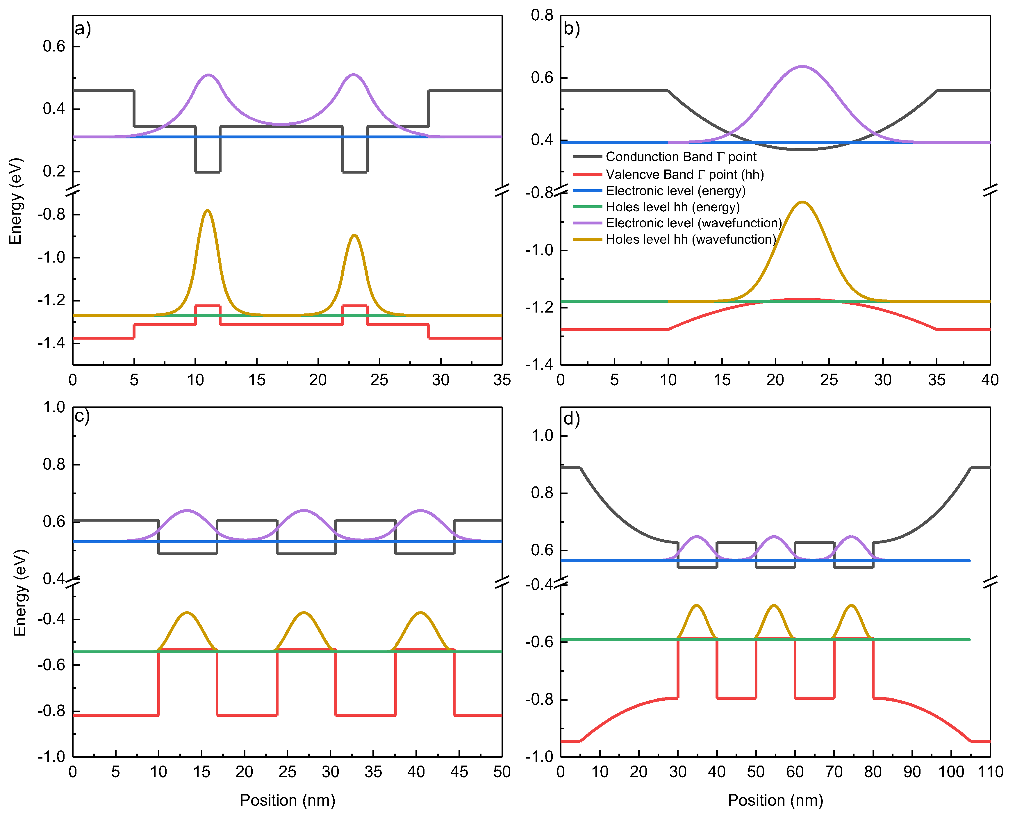
Figure 2.
Current – voltage characteristics of the investigated laser diodes.
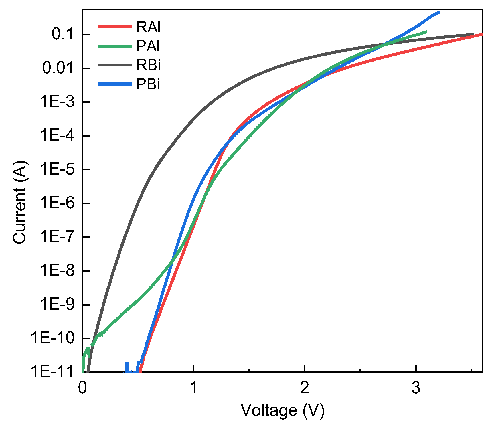
Figure 3.
Room temperature measurement of output power versus injection current dependences of LDs with the insets showing the emission spectra: a) laser RAl and b) laser PAl.
Figure 3.
Room temperature measurement of output power versus injection current dependences of LDs with the insets showing the emission spectra: a) laser RAl and b) laser PAl.
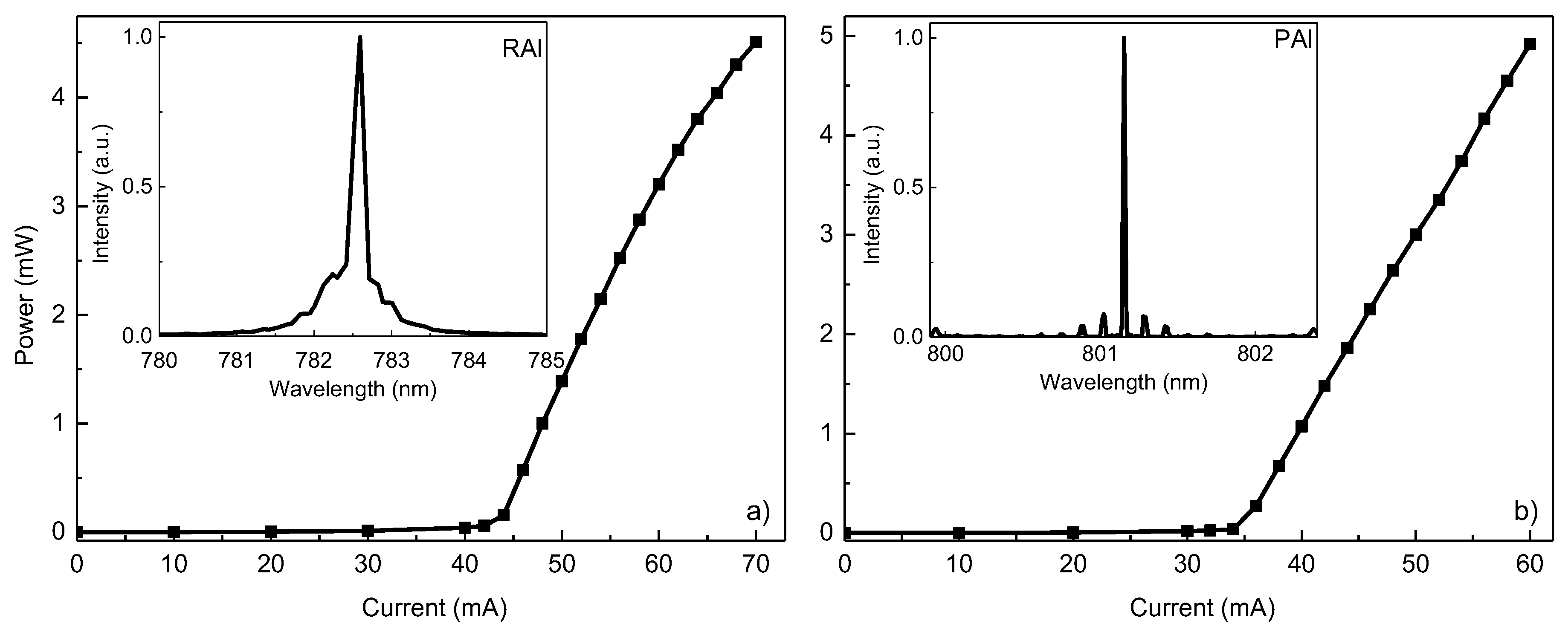
Figure 4.
Room temperature measurement of output power versus injection current (pulsed 50 ns at 1 kHz) dependences of LDs with the insets showing the emission spectra: a) laser RBI and b) laser PBi, black curve for the laser on thinned substrate, blue for before substrate thinning.
Figure 4.
Room temperature measurement of output power versus injection current (pulsed 50 ns at 1 kHz) dependences of LDs with the insets showing the emission spectra: a) laser RBI and b) laser PBi, black curve for the laser on thinned substrate, blue for before substrate thinning.
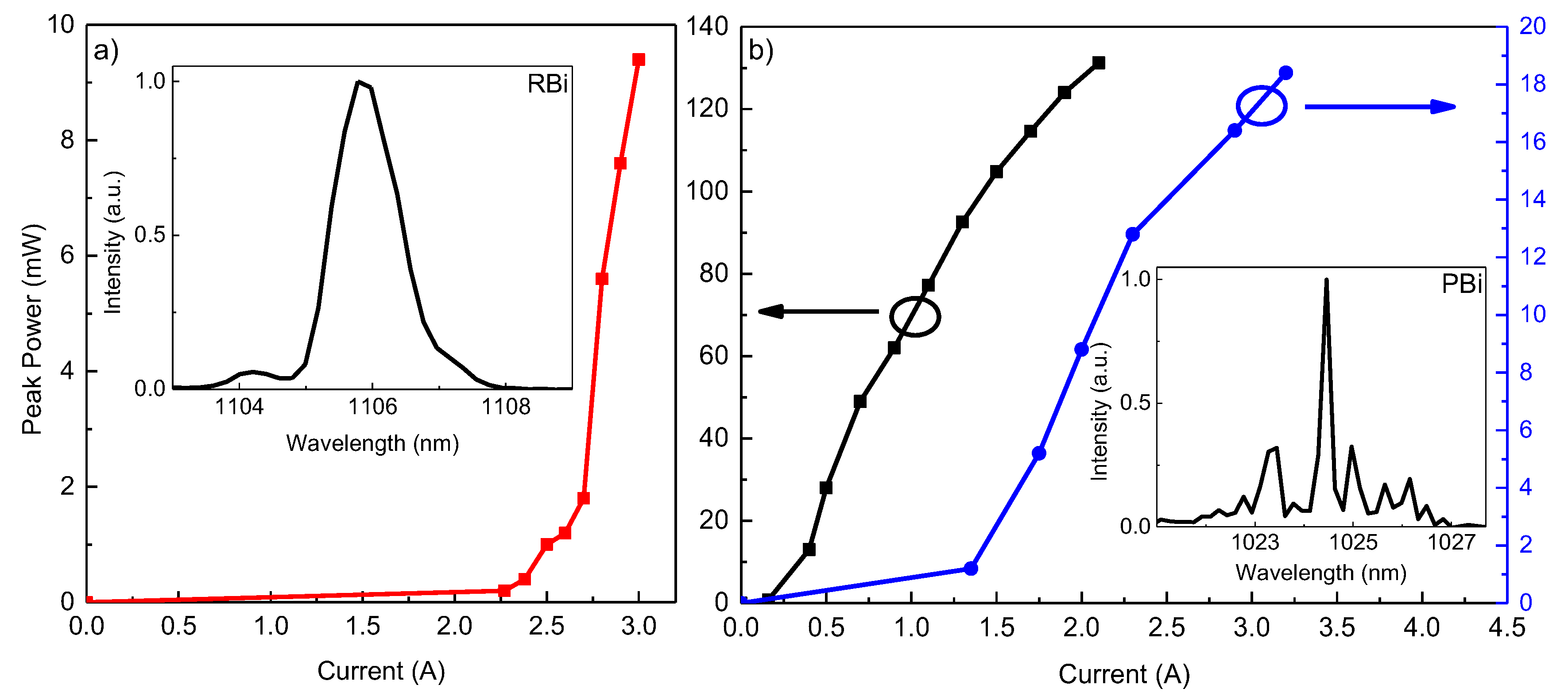

Table 1.
Structural parameters of the intrinsic regions of grown devices.
| Laser Diode | RAl | PAl | RBi | PBi |
|---|---|---|---|---|
| QW type | RQW | PGBs | RQW | RQW in PGBs |
| No of QW | 2 | 1 | 3 | 3 |
| QW composition | (Al, Ga)As | GaAsBi | ||
| QW thickness, nm | 2 | 25 | 6.8 | 10 |
| Parabolic grading | - | Al0.3 ↔ Al0.9 | - | Al0.3 ↔ Al0.0 |
| Barrier composition | Al0.15Ga0.85As | - | GaAs | GaAs |
| outer / inner barrier thickness |
5 / 10 | - | - / 7 | - / 10 |
| Spacer composition | Al0.30Ga0.70As | Al0.30Ga0.70As | GaAs | - |
| Spacer thickness, nm | 200 | 200 | 25 | - |
Disclaimer/Publisher’s Note: The statements, opinions and data contained in all publications are solely those of the individual author(s) and contributor(s) and not of MDPI and/or the editor(s). MDPI and/or the editor(s) disclaim responsibility for any injury to people or property resulting from any ideas, methods, instructions or products referred to in the content. |
© 2025 by the authors. Licensee MDPI, Basel, Switzerland. This article is an open access article distributed under the terms and conditions of the Creative Commons Attribution (CC BY) license (http://creativecommons.org/licenses/by/4.0/).
Copyright: This open access article is published under a Creative Commons CC BY 4.0 license, which permit the free download, distribution, and reuse, provided that the author and preprint are cited in any reuse.


