
Submitted:
27 March 2025
Posted:
31 March 2025
You are already at the latest version
Abstract
This study employs molecular dynamics simulations under tensile loads to thoroughly examine how variations in nanowire lengths and twin thicknesses affects the various mechanical properties; such as yield strength and deformation behaviors; like failure modes with cylindrical cross-sectioned silicon nanowires. It investigates the effects of nanowire length and twin thickness variations with the alignment of Σ3 CTBs along <001˃ axis. Analysis of nanowire models with lengths ranging from 70 to 100 nm and twin thicknesses between 2 and 10 nm reveals that longer nanowires exhibit superior mechanical performance while reduced twin thickness enhances both strength and ductility. Compared to single-crystal counterparts; longer twinned silicon nanowires consistently demonstrate significant mechanical improvements outperforming shorter ones. These variations also affect brittle-to-ductile and ductile-to-brittle transitions among other failure modes. Plastic deformation analysis indicates that both partial and full dislocation emissions from free surfaces affect the yield stress. Additionally; accumulation, propagation, and glide of dislocations near CTBs improved the yield stress and facilitated the ductile-to-brittle transition. This research provides valuable insights into how twin thickness and nanowire length affect the various mechanical properties of non-metallic materials and systems.
Keywords:
twinned
; silicon nanowires
; length
; mechanical properties
; molecular dynamics simulation
1. Introduction
Because of their excellent nanomechanical properties (such as ultra-high specific strength and strength-to-weight ratio, for example), 1D metallic nanostructures such as nanowires and nanotubes have been widely studied. One of the best aspects of 1D metallic nanowires for future applications has been their unique morphology, which consists of low-energy crystal facets, long segments of smooth crystal planes, and high defect density. Such applications could include nanoelectrochemical systems [1], and micro-electromechanical systems (MEMS) or nano-electromechanical systems (NEMS) [2,3]. Considering Lu et al. initial report [4], the nanotwinned metallic materials constituted of several coherent twin boundaries (CTBs) with thickness at the nanoscale have been of special interest. The authors found that the extremely high tensile strength (on the order of 1 GPa (versus 0. 25 GPa for the coarse-grained Cu) and the significant plastic strain (up to 14% for the Cu) obtained by adding CTBs into the metallic nanowire and metallic nanopillar materials – the ultrafine-grained face-centered cubic metals (FCC) with low stacking fault energy [5,6,7]. The mechanical properties of nanotwinned metals are attributed to the size-dependent interactions between dislocations and CTBs, as demonstrated experimentally [6,8,9], and molecular dynamics (MD) simulations [10,11,12,13,14]. In addition, twin boundaries (TBs) and sample size could also increase the strength of nanopillars [15,16,17,18,19]. As a result, unique defects must be added to NWs to increase the yield strength produced by the nucleation of dislocations from free surfaces and the obstruction of dislocations by CTBs without decreasing sample strength.
So, even though there has been a ton of research on how strong twinned metals can be [20,21,22,23,24], it turns out that they can achieve some pretty impressive theoretical strengths—like 3.12 GPa in twinned Au nanowires [20], and 2.43 GPa in twinned Cu nanopillars [21]. These are a big deal, especially when you compare them to single-crystal metal nanowires or nanopillars [20,25].
Since engineering CTBs came onto the scene, we have dug into the strength of twinned nanowires. But there is still a lot more to explore, especially about how the mechanical properties, fracture modes, and deformation processes of twinned non-metallic materials or systems with CTBs change based on the nanowire length (which is more of an external size factor) and the thickness of those twins (which is an internal size factor). It looks like the strength of metallic nanowires with twins gets a boost when the twin thickness increases [19,26,27], and also when the length of the nanowires increases [21].
Recent in-situ tensile experiments reveal that varying twin thickness leads to a brittle-to-ductile transition in twinned Cu nanopillars [21], and twinned Au nanowires [22]. Interestingly, the brittle and ductile fracture modes occur only within opposite twin thickness ranges. For Cu nanopillars, ductile fracture is observed when the twin thickness drops below a critical value of 3.4 nm, whereas in Au nanowires, it occurs when the twin thickness exceeds 2.8 nm. Moreover, the failure mode and brittle-to-ductile transition are influenced by both the nanowire’s twin thickness and geometry [13,21]. In twinned nanowires with orthogonally oriented coherent twin boundaries (CTBs), the yield strength improves due to dislocation emissions at the CTB surface intersection [19]. Additionally, differences in dislocation to CTB interactions enhance the mechanical properties and deformation behavior of various metallic nanowires [20].
In this study, we utilized MD simulations to investigate the mechanical properties on twinned silicon NWs subjected to uniaxial tensile loading. Nanowires featured <001˃ oriented coherent twin boundaries (CTBs) aligned parallel to their axis. Our focus was on understanding the yield strength fracture behavior and deformation mechanism for both single-crystal and twinned silicon NWs specifically examining the impacts of nanowire length and twin thickness to analyze the yield and dislocation mechanisms. We observed atomic configurations to evaluate dislocation emission, interactions between dislocations and CTBs, dislocation glide along CTBs, and the accumulation of dislocations at CTBs during plastic deformation.
2. Simulation Models and Methods
The <001˃ oriented twinned Si nanowires, featuring cylindrical cross-sections, were simulated by periodically repeating Σ3 CTBs along the [001] axis, as illustrated in Figure 1a–b. All nanowires maintained a fixed diameter of 14.60 nm, while their lengths (L0) varied from 70 to 100 nm and twin thicknesses (TT) ranged between 2 and 10 nm. The molecular dynamics (MD) simulations were conducted using LAMMPS [28], employing the Erhart and Albe (EA) [29] potential and the velocity Verlet algorithm to integrate the equations of motion with a time step of 2 fs. Periodic boundary conditions were applied along the [001] axis, with the nanowires free in all other directions. Initially, the nanowires underwent CG minimization at 0 K, followed by equilibration at 300 K for 20 ps under zero pressure (using a constant NPT ensemble). Subsequently, uniaxial stretching was applied at a strain rate of 1x10⁸/s in a canonical (NVT, constant volume and temperature) ensemble at 300 K. The axial stress was computed using the Virial theorem and deformed atomic volume. Additionally, the Identify Diamond Structure (IDS) [30] method was employed to detect defects and analyze the nanowires’ microstructure, distinguishing between cubic and hexagonal diamond structures during deformation.
3. Results and Discussion
3.1. Length-Dependent Mechanical Properties of Si NWs
Materials like nanowires nanopillars and nanotubes have mechanical properties affected with intrinsic and extrinsic sizes. Intrinsic size refers to the dislocation density twin boundary spacing and grain sizes. On the other hand variables like nanowire diameter and length, thin film thickness and nanopillar diameter influence the size of the test sample. This study examined the impact of twin thickness which is regarded as an intrinsic size effect and NW length which is regarded as an extrinsic size effect on the mechanical characteristics and mechanism of deformation of silicon nanowires both single-crystal and twinned.
Figure 2a–d show the engineering stress-strain curves of four Si <001> nanowires at lengths L0 = 70, 80, 90, and 100 nm. As can be seen from Figure 2a–d, in all cases, the tensile stress increases linearly with strain up to an elastic stage, followed by a sharp drop in stress in the plastic stage, respectively. For both twinned and single-crystal Si NWs, the tensile stress increased as the nanowires length increased from 70-100 nm. The higher-strength (14.26 GPa) are impressive for the 100 nm nanowires length, whereas the lower-strength (14.17 GPa) are impressive for the 70 nm nanowires length with twin-structure silicon nanowires. The length-dependent stress–strain curves of the twinned Si nanowires with TT = 2 nm, 5 nm, and 10 nm are displayed in Figure 2a–c. In Figure 2, the stress–strain curves of the <001> oriented single crystal Si nanowires are also displayed for comparison. The outcome showed that both brittle and ductile fracture modes were experienced by all of the twinned Si nanowires. As can be shown in the stress-strain curves in Figure 2a–c, the nanowires with smaller lengths (L0 < 70 nm for twinned Si nanowires and L0 < 110 nm for single crystal Si nanowires) display ductile failure in the ductile fracture mode, showing significant plasticity at the yield point. As the length of nanowires increased; there is a significant rise in the tensile stress as illustrated by stress-strain curve in Figure 2(a–d). The curve in Figure 2(a–c) reveal that single-crystal silicon nanowires with an initial length L0 of 110 nm along with twinned nanowires exceeding 70 nm in length exhibit brittle-failure characterized by brittle fracture mode suggesting notable flexibility near the peak or yielding point. The result data shows that both single crystal and twinned silicon nanowires undergoes a transitions from ductile-to-brittle behavior as their length increases regardless the thickness of twins; this implies that shorter nanowires failed in a ductile manner while longer ones failed in a brittle manner. Length–dependent stress-strain characteristics of twinned silicon nanowires with lengths of 70 nm, 80 nm, 90 nm, and 100 nm are presented in Figure 2a–c. Additionally; Figure 2d provides a comparison with the stress-strain curves of <001˃ oriented single-crystal silicon nanowires. A similar length-dependent ductile-to-brittle transition has been noted in twinned copper nanowires with coherent twin boundaries [13]. We begin by investigating how the length of nanowires affects the mechanical properties of silicon nanowires which is classified as an extrinsic size effect. The results from molecular dynamics simulations indicate that similar to single-crystal silicon nanowires the yield strength on twinned silicon nanowires also increases with length reinforcing the notion that “longer is stronger”. As illustrated in Figure 3, twinned silicon nanowires (Si NWs) exhibit higher yield stress compared to single-crystal Si NWs. For instance, when the twinned Si NW has a length of L0 = 70 nm increasing its length to 100 nm results in a rise in yield strength from 14.17 GPa to 14.26 GPa (9.0% increase). In contrast, single-crystal Si NWs show a minimal increase in yield strength from 12.72 GPa to 12.81GPa (9.0% increment). Yield stress marks the onset of plastic deformations with a stress stages divided into elastic, and plastic phases before and after this point respectively. To uncover the reasons behind the enhanced strength, the atomic processes occurring during deformations prior of fracture were analyzed, as shown in Figure 3. The findings reveal that for all nanowires; plasticity is driven by the nucleation of piled-up 1/2<110˃ {111} Full dislocations and 1/6<112˃ {111} partial dislocations. These dislocations interact with twin boundaries (TBs) and glide along them. This evidence demonstrates that twinned Si NWs possess superior mechanical properties influenced by a length-dependent size effect compared to their single-crystal counterparts.
3.2. Twin Thickness-Dependent Mechanical Properties of Si NWs
Twin thickness is observed to have a significant effect on both the plastic deformation and the failure mode of the twinned Si nanowires compared to Figure a–d. Figure 4 shows the stress-strain curves for the twinned Si nanowires with L0 = 70 nm, 80 nm, 90 nm, and 100 nm about twin thickness. This figure illustrates that irrespective of twin thickness, all short, twinned Si nanowires (L0 = 70 nm) fail via ductile fracture mode, while all long nanowires (L0 = 100 nm) fail via brittle fracture mode. This phenomenon generally indicates that medium-length twinned Si nanowires, as opposed to short or long nanowires are more likely to exhibit the failure mode (fracture) and the ductile-to-brittle transition, which is dependent on the twin thickness. The present results emphasize the significant correlation between twin thickness and the mechanical properties, along with the ductile-to-brittle transition, of the twinned silicon nanowires, which are influenced by the length of the nanowires. To solve the aforementioned problem, more MD simulations were run to determine the critical lengths for the failure mode and the ductile-to-brittle transition. Figure 4 depicts the failure mechanisms, fracture, and a transition from ductile-to-brittle behavior in twinned silicon nanowires (Si NWs) highlighting associated to the failure modes influenced by the twin thickness and length of the nanowires. Figure 4 categorizes the nanowires into three distinct sections based on their lengths. Our analysis of the impact of twin thickness on these failure modes and ductile-to-brittle transitions reveals that long nanowires (L0 > 70 nm) invariably exhibit a brittle failure mode designated as the brittle fracture mode region regardless of the twin thickness. In contrast, short nanowires (L0 < 70 nm) consistently show a ductile failure mode referred to as the ductile fracture mode region. Notably, a limited length range of 70 nm to 110 nm twin-free is critical for identifying ductile-to-brittle transitions, i.e. influenced by twin thickness as illustrated in Figure 4. This indicates that within the specific length range of 70 to 110 nm (twin-free), a decrease in twin thickness leads to a ductile-to-brittle transition. Beyond this range long twinned Si NWs continue to display a brittle failure mode while short twinned Si NWs maintain a ductile failure mode. Conversely, the ductile-to-brittle transition is consistently observed and remains unaffected by twin thickness when analyzing the effect of length on the failure mode. According to Figure 4, as the twin thickness increases, so does the critical length for the failure (fracture) mode and the ductile-to-brittle transition. From 100 nm to 70 nm, the critical length falls gradually when the twin thickness decreases from 10 nm to 2 nm. Figure 4 illustrates the drastic decrease in thickness. A single atomic layer appears that lies between two CTBs at the minimum twin thickness of 2 nm, at which point there is an immediate decrease in the critical length. When the twin thickness decreases to 2 nm, there exists a dramatic reduction in the critical length, followed by a gradual decrease for the twinned Si nanowires that contained CTBs. Therefore, we conclude that the nanowires’ brittle failure mode (fracture) can be helped by the highest amount of CTBs. We first explored the effect of NW length and then the effect of NW twin thickness, which is also known as the intrinsic size effect, on the mechanical properties of Si NWs. The results illustrated in Figure 5 indicate that the yield strength of single-crystal silicon nanowires (Si NWs) and twinned Si NWs exhibited an increase as the twin thickness was increased, thereby supporting the notion that “longer is stronger”. As illustrated in Figure 5, the twinned silicon nanowires demonstrated a higher yield stress compared to single crystal counterpart. This research indicated that in contrast to shorter NWs the longer Si NWs exhibit a significant dependence on twin thickness which can be interpreted as an intrinsic size effect. Specifically the yield strength of twinned Si NWs with an initial length L0 = 70 nm increased by 69% relative to single crystal Si NWs while the yield strength for longer twinned Si NWs with L0 = 100 nm showed a 56% increase. Notably the strengthening effect was more pronounced in the longer Si NWs. This observation led to the conclusion that the length of the NWs which includes multiple coherent twin boundaries (CTBs) is where the strengthening effect is most evident. Recent experimental and molecular dynamics (MD) simulation studies on face-centered cubic (FCC) metallic nanowires or nanopillars have reported similar CTBs strengthening effects in longer NWs [13,15,18,20,31,32,33]. Furthermore; these studies emphasized the need for future investigations focused on the development of nanotwinned metals and the design of nanoscale mechanical system consequently the exploration of length-dependent mechanical behaviors and deformation mechanisms in twinned non-metallic NWs has not been entirely neglected. This finding is crucial for enhancing our understanding of the yield strength of one-dimensional twinned NWs and for the advancement of nanoscale nanotwinned non-metallic materials and systems that incorporate CTBs. This research specifically analyzed the influence of twin thickness and NW length on the mechanical behaviors, and deformation mechanisms of twinned Si NWs with CTBs aligned along the <001> direction, addressing a previously identified issue in light of this prior research challenge [4,13,15,18,20,31,32,33]. The mechanical properties and deformations mechanism for twinned Si NWs with CTBs oriented in the <001> direction were thoroughly examined in relation to twin thickness and NW length [4,13,15,18,20,31,32,33].
3.3. Observation of Mechanical and Deformation Behaviors of Si NWs
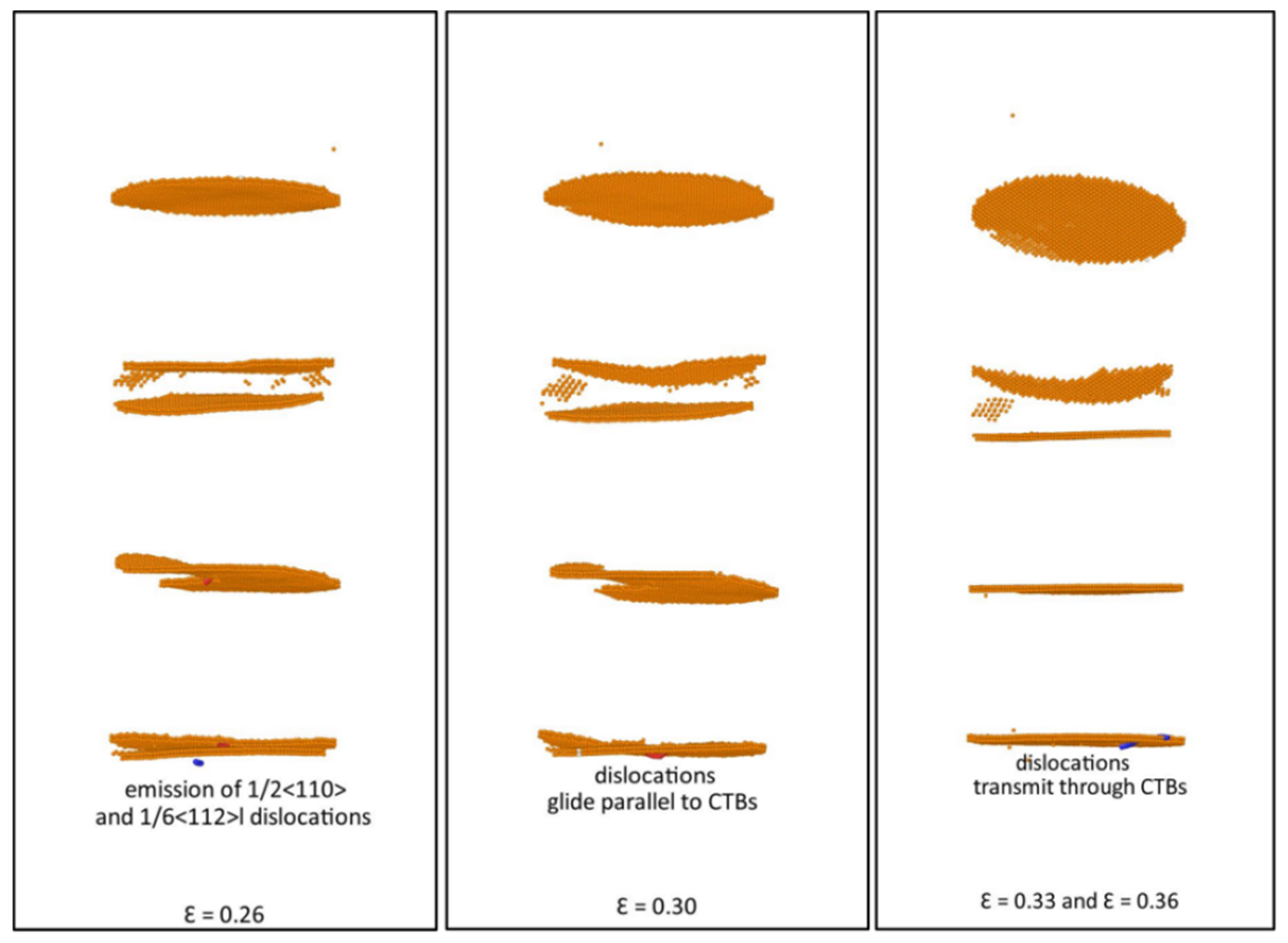
The atomic configurations of the twinned silicon nanowires were analyzed to investigate the effect of twin thickness and nanowire length on yield strength and the deformation process. For example, the first plasticity event is aided by the emission of 1/2 <110> Full and 1/6 <112> {111}. Partial dislocations at the strain of ε = 0.26 for the twinned Si NWs with L0 = 70 nm and twin thickness = 5 nm, as illustrated in Figure 6. A dislocation pile-up occurs at the CTBs at a strain of Ɛ = 0.26 as a result of the first dislocation nucleating from the free surface. Before fracture (failure), both full and partial dislocations begin to glide parallel to the CTBs in twinned Si NWs with CTBs oriented along the <001> direction under a continuous strain of ε = 0.30. All the piled-up dislocations eventually transmit/penetrate through the CTBs, which become accountable for the augmentation of yield strength at strains of ε = 0.33 and ε = 0.36. The results of this study indicate that the yield strength of twinned silicon nanowires (Si NWs) is consistently superior to that of their single crystal equivalents, with an increase in yield strength corresponding to greater twin thickness. This observation highlights the significant strengthening effect of coherent twin boundaries (CTBs). Furthermore, the research reveals that the yield strength of twinned Si NWs also increases with an increase in nanowire length. Our analysis demonstrates that the nucleation of dislocations at the free surface, their accumulation at the CTBs, and their movement parallel to the CTBs before fracture contribute to the onset of plastic deformation, as depicted in Figure 6.
4. Conclusions
Using molecular dynamics simulations, we examine in this study how the mechanical properties and deformation mechanisms of both twinned and single-crystal silicon nanowires are affected by varying nanowire lengths and the thickness of twin structures. The twinned silicon nanowires, which have a cylindrical cross-section, were created with coherent twin boundaries (CTBs) parallel to the axis of the nanowires and aligned along the <001> direction.
- ▪
- Our simulation findings indicate that the mechanical properties of the twinned silicon nanowires are significantly affected by the length of the nanowires, which is regarded as an extrinsic size effect, and the thickness of the twins, which is considered an intrinsic size effect. This demonstrates a pronounced impact of both nanowire length and twin thickness on yield strength and deformation mechanisms. Depending on the effects of the nanowire length and twin thickness, the twinned Si nanowires undergo ductile as well as brittle failure modes (fracture) and ductile-to-brittle transition. When the twin thickness is increased, the twinned Si nanowires undergo a ductile-to-brittle transition as the critical length increases from 70 nm to 100 nm. When compared to single-crystal nanowires, twinned Si nanowires exhibit a strong NW length effect (longer is stronger) and a strong twin thickness effect (thinner is stronger).
- ▪
- The mechanical behaviors for twinned Si NWs were demonstrated to be considerably improved by Σ3 coherent twin boundaries (CTBs). It was observed that longer nanowires exhibit a more pronounced strengthening effect whereas shorter nanowires experience a diminished strengthening response.
- ▪
- It was found that 1/2<110> {111} full dislocations and 1/6<112> {111} partial dislocations were produced from the free surface near the coherent twin boundaries (CTBs) by analyzing atomic configurations during the early stages of plastic deformation. On the other hand, dislocations were shown to accumulate at these TBs as they glided parallel to the CTBs under specific strain levels. As a result, the dislocations’ buildup and migration accross the CTBs affect the twinned silicon nanowires’ yield strength.
The present investigation proposes an insight into the mechanical properties and deformation mechanisms of twinned non-metallic nanowires or systems featuring <001>-oriented Σ3 coherent twin boundaries (CTBs) aligned with the axis of the nanowires. This research emphasizes the effect of twin thickness, regarded as an intrinsic size effect, alongside the length of the nanowires, which is regarded as an extrinsic size effect.
Author Contributions
Q.X.; Validation, Formal analysis, Data curation: M.Y.; Writing–original draft, Methodology: M.Y.; Writing–review and editing, Methodology.
Funding
The work is supported the National Natural Science Foundation of China (NSFC).
Data Availability Statement
Data will be made available on request.
Conflicts of Interest
The authors declare no conflicts of interest. The authors declare that they have no known competing financial interests or personal relationships that could have appeared to influence the work reported in this paper.
References
- A. Husain, J. Hone, H.W.Ch. Postma, X.M.H. Huang, T. Drake, M. Barbic, A. Scherer, M.L. Roukes, Nanowire-based very-high-frequency electromechanical resonator, Applied Physics Letters 83 (2003) 1240–1242. [CrossRef]
- M. Liao, S. Hishita, E. Watanabe, S. Koizumi, Y. Koide, Suspended Single-Crystal Diamond Nanowires for High-Performance Nanoelectromechanical Switches, Advanced Materials 22 (2010) 5393–5397. [CrossRef]
- Zheng Fan, Miao Yu, Xinyong Tao, R. Shanmugam, Xudong Fan, Wei Lai, Lixin Dong, In situ investigation of nanoelectrochemical systems, in: 14th IEEE International Conference on Nanotechnology, IEEE, Toronto, ON, 2014: pp. 882–883. [CrossRef]
- Y.T. Zhu, X.Z. Liao, X.L. Wu, Deformation twinning in nanocrystalline materials, Progress in Materials Science 57 (2012) 1–62. [CrossRef]
- K. Lu, L. Lu, S. Suresh, Strengthening Materials by Engineering Coherent Internal Boundaries at the Nanoscale, Science 324 (2009) 349–352. [CrossRef]
- Y.F. Shen, L. Lu, Q.H. Lu, Z.H. Jin, K. Lu, Tensile properties of copper with nano-scale twins, Scripta Materialia 52 (2005) 989–994. [CrossRef]
- M. Dao, L. Lu, Y.F. Shen, S. Suresh, Strength, strain-rate sensitivity and ductility of copper with nanoscale twins, Acta Materialia 54 (2006) 5421–5432. [CrossRef]
- A.M. Hodge, Y.M. Wang, T.W. Barbee, Mechanical deformation of high-purity sputter-deposited nano-twinned copper, Scripta Materialia 59 (2008) 163–166. [CrossRef]
- N. Li, J. Wang, S. Mao, H. Wang, In situ nanomechanical testing of twinned metals in a transmission electron microscope, MRS Bull. 41 (2016) 305–313. [CrossRef]
- X. Li, Y. Wei, L. Lu, K. Lu, H. Gao, Dislocation nucleation governed softening and maximum strength in nano-twinned metals, Nature 464 (2010) 877–880. [CrossRef]
- L. Zhu, H. Ruan, X. Li, M. Dao, H. Gao, J. Lu, Modeling grain size dependent optimal twin spacing for achieving ultimate high strength and related high ductility in nanotwinned metals, Acta Materialia 59 (2011) 5544–5557. [CrossRef]
- J. Sun, L. Fang, K. Sun, J. Han, Direct observation of dislocations originating from perfect twin boundaries, Scripta Materialia 65 (2011) 501–504. [CrossRef]
- J. Sun, L. Fang, A. Ma, J. Jiang, Y. Han, H. Chen, J. Han, The fracture behavior of twinned Cu nanowires: A molecular dynamics simulation, Materials Science and Engineering: A 634 (2015) 86–90. [CrossRef]
- T. Zhu, H. Gao, Plastic deformation mechanism in nanotwinned metals: An insight from molecular dynamics and mechanistic modeling, Scripta Materialia 66 (2012) 843–848. [CrossRef]
- K.A. Afanasyev, F. Sansoz, Strengthening in Gold Nanopillars with Nanoscale Twins, Nano Lett. 7 (2007) 2056–2062. [CrossRef]
- A.J. Cao, Y.G. Wei, S.X. Mao, Deformation mechanisms of face-centered-cubic metal nanowires with twin boundaries, Applied Physics Letters 90 (2007) 151909. [CrossRef]
- Y. Zhang, H. Huang, Do Twin Boundaries Always Strengthen Metal Nanowires?, Nanoscale Res Lett 4 (2009) 34. [CrossRef]
- C. Deng, F. Sansoz, Enabling Ultrahigh Plastic Flow and Work Hardening in Twinned Gold Nanowires. Nano Lett 2009, 9, 1517–1522. [CrossRef] [PubMed]
- C. Deng, F. Sansoz, Size-dependent yield stress in twinned gold nanowires mediated by site-specific surface dislocation emission, Applied Physics Letters 95 (2009) 091914. [CrossRef]
- C. Deng, F. Sansoz, Fundamental differences in the plasticity of periodically twinned nanowires in Au, Ag, Al, Cu, Pb and Ni, Acta Materialia 57 (2009) 6090–6101. [CrossRef]
- D. Jang, X. Li, H. Gao, J.R. Greer, Deformation mechanisms in nanotwinned metal nanopillars, Nature Nanotech 7 (2012) 594–601. [CrossRef]
- J. Wang, F. Sansoz, J. Huang, Y. Liu, S. Sun, Z. Zhang, S.X. Mao, Near-ideal theoretical strength in gold nanowires containing angstrom scale twins, Nat Commun 4 (2013) 1742. [CrossRef]
- C. Deng, F. Sansoz, Near-Ideal Strength in Gold Nanowires Achieved through Microstructural Design, ACS Nano 3 (2009) 3001–3008. [CrossRef]
- Z.X. Wu, Y.W. Zhang, M.H. Jhon, J.R. Greer, D.J. Srolovitz, Nanostructure and surface effects on yield in Cu nanowires, Acta Materialia 61 (2013) 1831–1842. [CrossRef]
- T. Zhu, J. Li, S. Ogata, S. Yip, Mechanics of Ultra- Strength Materials, (n.d.).
- H.Y. Song, Y. Sun, Effect of coherent twin boundary and stacking fault on deformation behaviors of copper nanowires, Computational Materials Science 104 (2015) 46–51. [CrossRef]
- J. Wang, F. Sansoz, C. Deng, G. Xu, G. Han, S.X. Mao, Strong Hall–Petch Type Behavior in the Elastic Strain Limit of Nanotwinned Gold Nanowires, Nano Lett. 15 (2015) 3865–3870. [CrossRef]
- S. Plimpton, Fast Parallel Algorithms for Short- Range Molecular Dynamics, (n.d.).
- P. Erhart, K. Albe, Analytical potential for atomistic simulations of silicon, carbon, and silicon carbide, Phys. Rev. B 71 (2005) 035211. [CrossRef]
- E. Maras, O. Trushin, A. Stukowski, T. Ala-Nissila, H. Jónsson, Global transition path search for dislocation formation in Ge on Si(001), Computer Physics Communications 205 (2016) 13–21. [CrossRef]
- J. Han, L. Fang, J. Sun, Y. Han, K. Sun, Length-dependent mechanical properties of gold nanowires, Journal of Applied Physics 112 (2012) 114314. [CrossRef]
- J. Sun, C. Li, J. Han, X. Shao, X. Yang, H. Liu, D. Song, A. Ma, Size Effect and Deformation Mechanism in Twinned Copper Nanowires, Metals 7 (2017) 438. [CrossRef]
- G.-W. Zhang, Z.-L. Yang, G. Luo, Investigation of mechanical properties of twin gold crystal nanowires under uniaxial load by molecular dynamics method, Chinese Phys. B 25 (2016) 086203. [CrossRef]
Figure 1.
Atomic model of twinned Si nanowires with parallel Σ3 CTBs. (a) full atomic view; (b) sectional view of CTBs.
Figure 1.
Atomic model of twinned Si nanowires with parallel Σ3 CTBs. (a) full atomic view; (b) sectional view of CTBs.
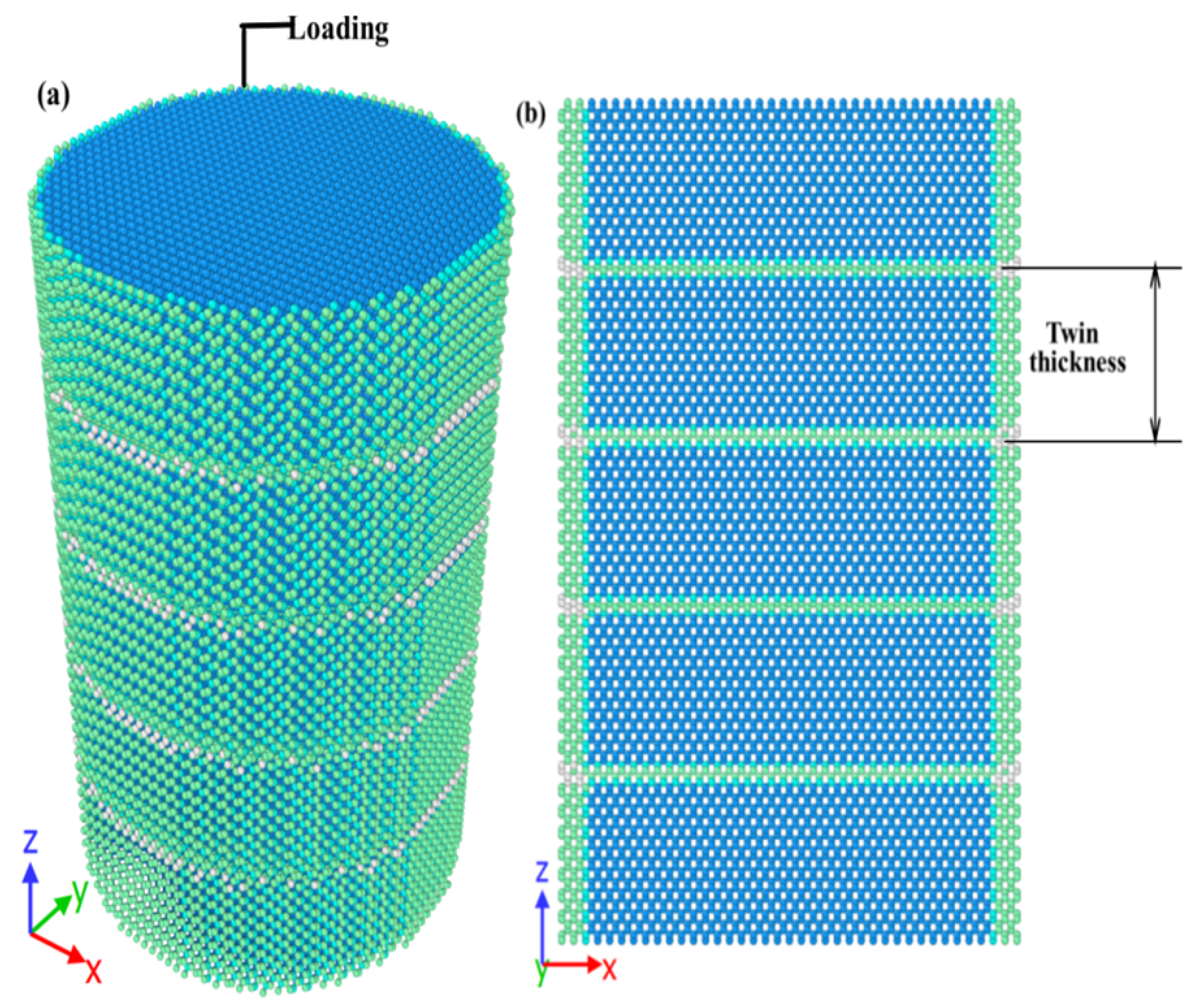
Figure 2.
Engineering stress–strain curves of the twinned Si nanowires with (a) TT = 2 nm (b) TT = 5 nm (c) TT = 10 nm (d) Single crystal Si nanowires.
Figure 2.
Engineering stress–strain curves of the twinned Si nanowires with (a) TT = 2 nm (b) TT = 5 nm (c) TT = 10 nm (d) Single crystal Si nanowires.
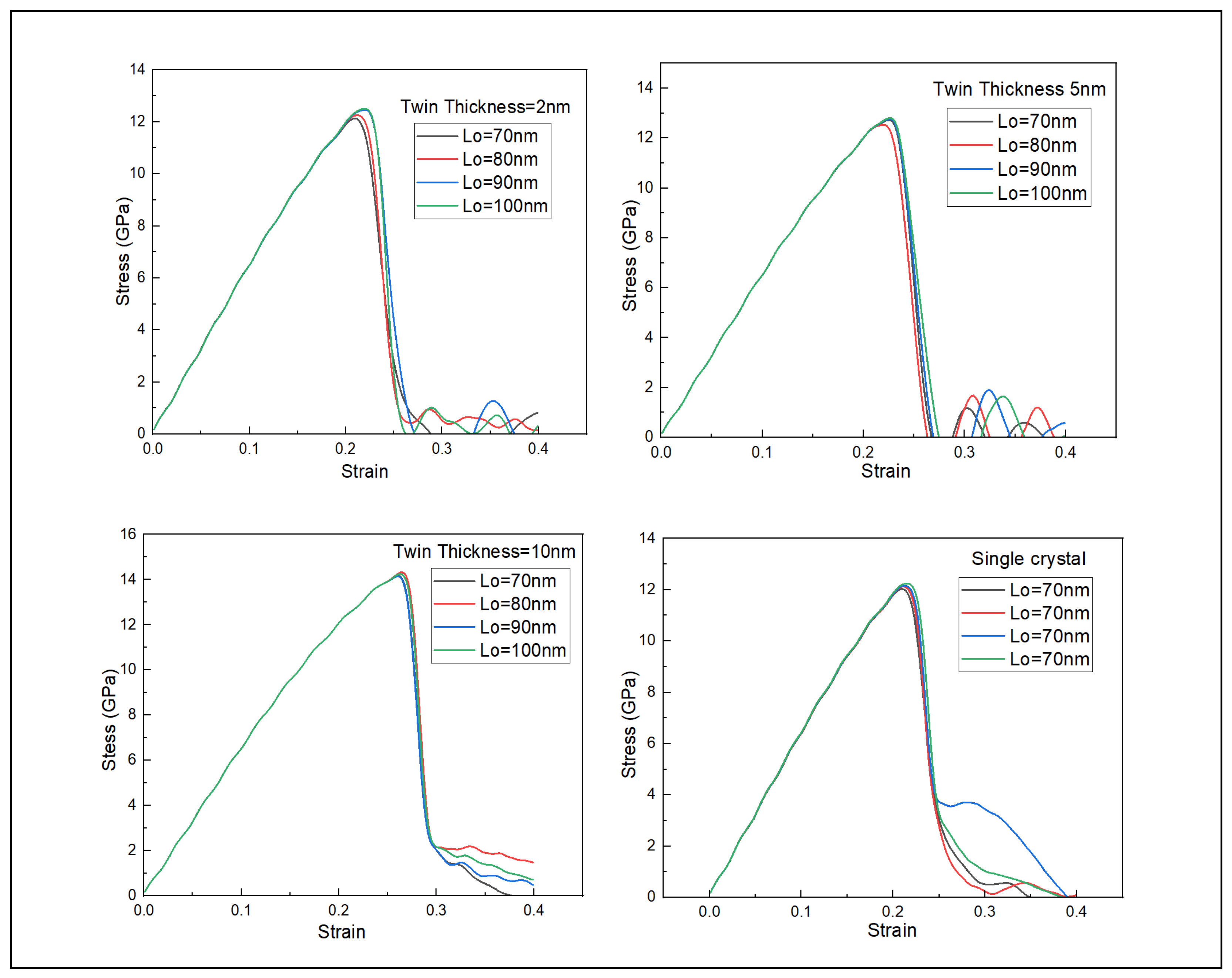
Figure 3.
Yield stress of twinned Si nanowires as a function of nanowire length, showing the size-dependent mechanical properties.
Figure 3.
Yield stress of twinned Si nanowires as a function of nanowire length, showing the size-dependent mechanical properties.
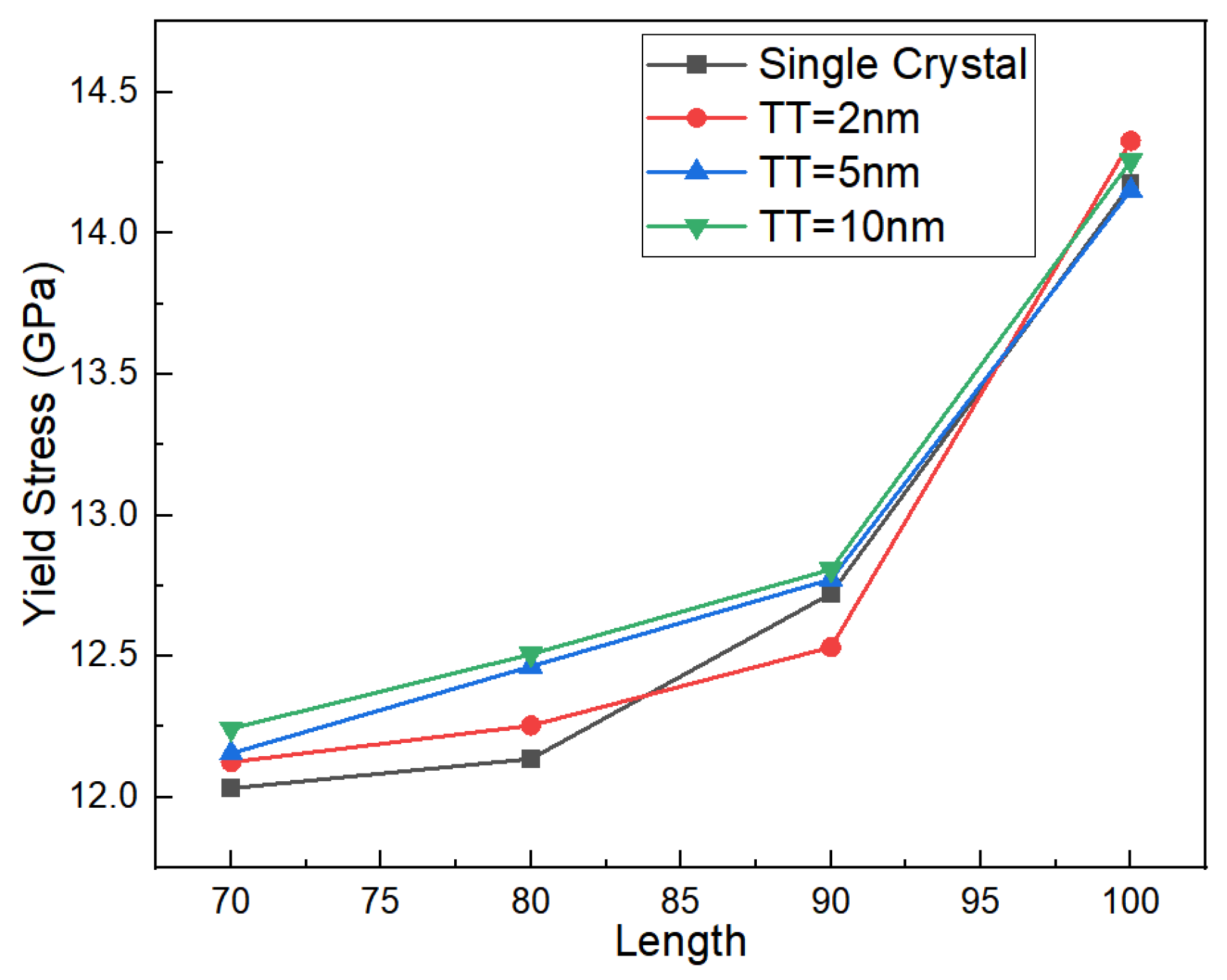
Figure 4.
Engineering stress–strain curves of the twinned Si nanowires with (a) L0 = 70 nm; (b) L0 = 80 nm; (c) L0 = 90 nm and (d) L0 = 100 nm.
Figure 4.
Engineering stress–strain curves of the twinned Si nanowires with (a) L0 = 70 nm; (b) L0 = 80 nm; (c) L0 = 90 nm and (d) L0 = 100 nm.
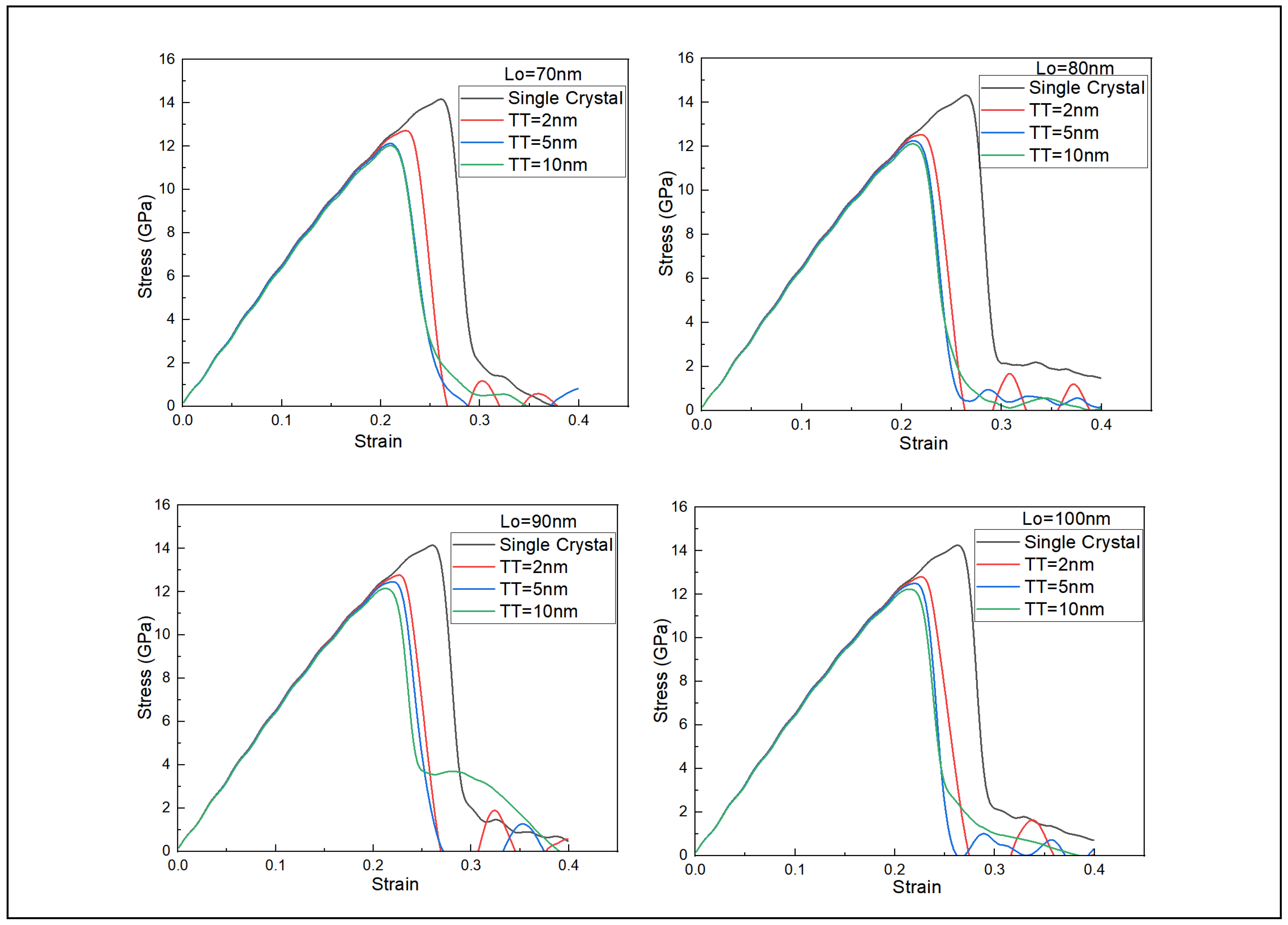
Figure 5.
Yield stress of twinned Si nanowires as a function of twin thickness.
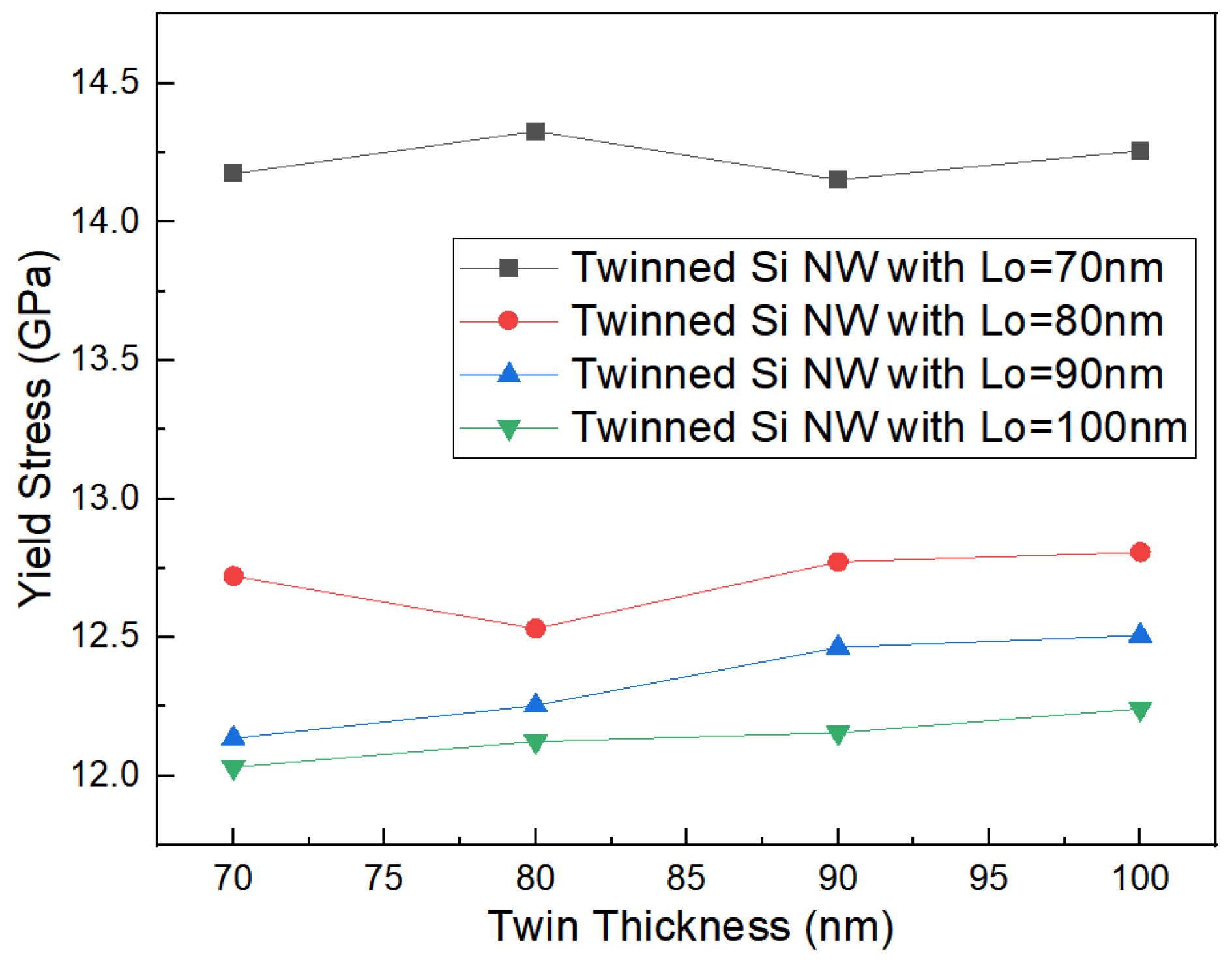
Figure 6.
Dislocation behavior of twinned Si nanowires with L0 = 70 nm and twin thickness = 5 nm during stretching at the stain of ε = 0.26 ε = 0.30 ε = 0.33 and ε = 0.36.
Figure 6.
Dislocation behavior of twinned Si nanowires with L0 = 70 nm and twin thickness = 5 nm during stretching at the stain of ε = 0.26 ε = 0.30 ε = 0.33 and ε = 0.36.
Disclaimer/Publisher’s Note: The statements, opinions and data contained in all publications are solely those of the individual author(s) and contributor(s) and not of MDPI and/or the editor(s). MDPI and/or the editor(s) disclaim responsibility for any injury to people or property resulting from any ideas, methods, instructions or products referred to in the content. |
© 2025 by the authors. Licensee MDPI, Basel, Switzerland. This article is an open access article distributed under the terms and conditions of the Creative Commons Attribution (CC BY) license (https://creativecommons.org/licenses/by/4.0/).
Copyright: This open access article is published under a Creative Commons CC BY 4.0 license, which permit the free download, distribution, and reuse, provided that the author and preprint are cited in any reuse.


