
Submitted:
27 March 2025
Posted:
28 March 2025
You are already at the latest version
Abstract
Lowpass filters with bandwidths larger than several GHz are required in many applications, such as anti-aliasing filters in high-speed ADCs and pulse-shaping filters in high-speed DACs. In highly integrated applications, low area occupation and power consumption are key specifications, so that inductor-less implementations are to be preferred. Furthermore, full CMOS implementations provide an advantage in terms of technology availability and cost. In this paper we present an inductor-less CMOS biquad stage based on the super source follower topology, that provides 8GHz cut-off frequency and a low power consumption of 0.42mW per pole, showing remarkable performance also in terms of bandwidth and dynamic range. The availability of two separate current sources allows independent tuning of natural frequency and quality factor. The stage can be implemented in two complementary ways, exploiting NMOS and PMOS input devices respectively, thus simplifying cascadability. The two complementary biquads have been implemented in the STMicroelectronics FDSOI 28nm CMOS process and extensively simulated, and provide stable performance under PVT variations and mismatches. The area occupation is about 387.5mm2 per biquad, one of the lowest in the literature. The figures-of-merit are remarkable, as the filters achieve excellent power efficiency, very low area occupation, and good dynamic range.
Keywords:
CMOS integrated circuits
; analog filters
; lowpass filters
; inductor-less filters
; anti-aliasing filters
1. Introduction
The recent diffusion of wideband communication systems [1,2,3] and high frequency measurement systems [4] drives the development of analog-to-digital (ADC) [3,5,6] and digital-to-analog (DAC) converters [7] operating with sampling frequencies of tens of GHz. Such converters usually require lowpass filters (LPFs) with bandwidth ranging from DC to GHz frequencies, to be used as anti-aliasing filters in ADCs and shaping filters in DACs. To allow processing very wide signal bandwidths, digitizer architectures based on the multiply-filter-processing (MFP) paradigm have been proposed [4,8,9], and they also require LPFs with GHz bandwidths. All these applications usually require high-order filters, to achieve a large out-of-band suppression, and they can be implemented by cascading biquad stages with suitable resonance frequencies and quality factors. Technology limitations pose constraints on the maximum quality factor that can be achieved, and this can be coped with by a suitable system design of the overall filter [10]. Noise and distortions, that determine the dynamic range of the filter, are the main design specifications; the high level of integration of the systems adds further requirements on the minimization of power consumption and area footprint.
Active filters are usually designed according to the gyrator synthesis method starting from an LC-ladder prototype [11,12], to the leapfrog LC-ladder simulation technique [13] or as a cascade of biquadratic sections (biquad) [10,14,15,16]. In the GHz frequency range, the traditional approach to design filters involves the use of real inductors in such active structures or in passive networks [17,18]. The use of inductors however is in contrast with the requirements of high integration, since on-chip inductors require a huge amount of area and are prone to electromagnetic interferences. Moreover, the constraints on practically realizable inductance values could lead to high power consumption, and the low quality factor and the large parasitic effects could limit the design space to achieve the desired frequency response.
The design of multi-GHz filters that do not use physical inductors is therefore an active field of research, and several lowpass and bandpass filters have been proposed in the literature. The most common approaches are the Gm-C architecture in the few-GHz range [11,12,13,14] and the use of RLC reference structures with active inductors [16,19,20,21,22] for frequencies around 10GHz. Low-frequency approaches such as the Sallen-Key [15,23,24] and Tow-Thomas biquads [25] have also been reported, and availability of deep sub-micron CMOS and SiGe BiCMOS technologies with fT of hundreds of GHz [26,27] has allowed applying the Sallen-Key architecture up to 17GHz [28].
While BiCMOS technologies surely allow very high frequencies using such low-frequency approaches, the trend towards the use of CMOS technologies for ever higher frequencies leads to exploring the design of inductor-less biquads operating at 10GHz in CMOS. In this context, open-loop architectures, such as Gm-C and the use of active inductors, seem preferable to closed-loop ones to achieve high frequencies. For low frequency applications, open-loop active-C biquad structures based on the flipped voltage follower (FVF) and super source follower (SSF) topologies have been proposed, and they appear to be a good candidate to achieve CMOS biquads with GHz-range frequencies and low power consumption [29,30,31,32,33]. A 7.5GHz biquad based on the FVF-C approach was proposed in [34] using a 28nm CMOS technology. It extends to high frequencies the approach used in [32], but the availability of a single control terminal makes it impossible to separate the control of the resonance pulsation ωo and of the quality factor Q. Tuning of ωo and Q would instead be useful both to compensate process variations and to allow the tunability of the filter, to adapt it to different applications.
In this paper we propose a biquad architecture based on the use of the SSF that allows achieving a 3dB bandwidth of 8GHz in a 28nm FDSOI CMOS technology with a power consumption below 1mW. The architecture can be implemented in two complementary forms (NMOS input and PMOS input), thus allowing an easy cascadability overcoming the different input and output voltage levels in the SSF topology. The SSF topology allows separate (and ideally orthogonal) tuning of ωo and Q of the biquad, thus improving with respect to the filter in [34].
2. Analysis of the Topology
This Section analyzes the proposed biquad topology in terms of frequency response, impact of parasitic effects, and large-signal performance.
2.1. Analysis of the SSF-Based Biquad
Inductor-less biquads usually are based either on closed-loop architectures (Sallen-Key, Tow-Thomas) or on open-loop structures such as Gm-C, active-C or RLC equivalents exploiting active inductors. With the goal of maximizing the resonance frequency for a given power level, open-loop architectures have a net advantage, and in particular the simpler topology creates fewer extra poles and zeros that affect the high frequency behavior of the biquad, limiting the maximum cut-off frequency.
As a consequence, the source-follower-C (SF-C) filter class is a good candidate to design biquads with very high cut-off frequency and good overall performance, since they use a limited number of devices, and hence of internal nodes that add extra poles that are desired to be out of band. In particular, biquads based on the flipped voltage follower (FVF) and on the super source follower (SSF) topologies have been proposed in the literature, aimed at low frequency biomedical applications [29,30,31,32,33].
Figure 1 shows the topology of FVF and SSF stages: by an analysis of the schematics, it is clear that their small-signal behavior is identical, since the SSF can be interpreted as the folded version of the FVF. They both form a unitary-gain loop with the same input and output impedances and voltage and current gains. However, the folded nature of the SSF yields more flexibility in accommodating voltage swings at the internal high impedance node: thus we select it to design a multi-GHz lowpass biquad. The structure can be considered as a current-mode circuit [35,36,37,38]: M1 is an inverting second-generation current conveyor (CCII) [36], whereas M2 is a transconductance. The combination of the two yields a CFOA (current-feedback operational amplifier) [37] without the output low-impedance stage.
It has to be noted that source follower structures provide a DC level shift between input and output equal to a gate-source voltage. While this is not an issue for a single biquad, it can impair the cascading of stages to achieve higher-order filters with a limited supply voltage range. However, the complementary nature of CMOS technology allows overcoming this issue, by alternating stages based on NMOS and PMOS input devices (N-type and P-type biquads in the following), as shown in Figure 2.
2.2. Ideal Frequency Response
The proposed biquad, shown in Figure 2 in the N-type and P-type configurations, is composed of a super source follower with two additional capacitors, one between the output node and the internal high-impedance node, and the other between the output node and ground. In practice, transistor M1 acts as a current conveyor with the gate as Y terminal, the source as X terminal and the drain as Z terminal; the high-impedance load at the Z terminal and the common-source amplifier (M2) close the feedback loop. The current generator IB1 sets the bias current of M1, whereas current generator IB2 draws the sum of the currents of M1 and M2: having two current sources allows easier tuning of biquad parameters than in the FVF case [34], as we will show in the following.
Figure 3 shows the small-signal equivalent circuit of the proposed topology: transistors M1 and M2 are modeled by their transconductance , their output conductance , where is the intrinsic gain of the device, and their gate-source capacitance is . Current sources are modeled by their output conductances . Gate-drain capacitances are neglected.
Neglecting the capacitances and the output conductances of the transistors, the ideal transfer function can be easily calculated as
where
Because and are functions of the biasing currents of the corresponding transistors, it is possible to tune the frequency response to compensate the variations of both and . Scaling the two currents by the same amount leaves the ratio roughly unchanged and ideally affects only . On the other hand, changing the two currents in opposite directions has a larger impact on and ideally no impact on . The control could therefore independently set the ratio and product of the ’s to set the two parameters separately, because they will impact the two parameters differently. Because the filter is in unity feedback configuration, the low-frequency gain is always close to 0dB at DC and cannot be tuned.
In the following subsections, we will analyze the impact of parasitic elements of the transistors on the transfer function (1).
2.3. Effect of Parasitic Capacitances
The two main parasitic capacitances in Figure 3 are the of the two transistors M1 and M2. We assume for simplicity that for both transistors, with , . The frequency response of the biquad, including these capacitances, can be calculated from the circuit in Figure 3, neglecting the conductances , as:
The impact on the poles is limited if , but two negative zeros appear. Unfortunately, the second-order term at the numerator is large with respect to the first-order term, so that the zeros will be complex conjugated with large quality factor:
Because the number of zeros is equal to the number of poles, the gain at infinity is finite:
However, the asymptotic gain is low if . It has to be noted that the zeros set a limit to the maximum bandwidth that can be achieved for a given level of out-of-band attenuation.
For what concerns the poles of the biquad, the expressions for the resonance frequency and the quality factor are reported below:
Equations show that the resonance frequency is slightly reduced by the additional capacitances, whereas the impact on the quality factor can be positive or negative.
2.4. Effect of Parasitic Resistances
There are two nodes in the circuit where the parasitic resistances of the current generators and of M1 and M2 are present. M1 adds a parasitic resistance in parallel with , the other devices add parasitic resistances from one of the two nodes (output and high-impedance internal node) toward ground.
To make this analysis more meaningful, we assume that all output conductances are proportional to the respective transconductances as
where (the intrinsic gain of the transistor) in case of simple transistors (i.e. ) and in case of cascodes. Moreover, we assume and , i.e. the output conductances of the current sources are proportional to their currents, and devices implementing them are sized with the same overdrive voltage as M1 and M2.
With these assumptions, the frequency response is:
Eq. (11) shows that parasitic resistances reduce the DC gain, slightly increase the resonance frequency, and reduce the quality factor. No additional poles or zeros are created.
The most interesting effect of the parasitic resistances is that they result in a maximum quality factor that can be achieved by using this biquad topology. Defining the capacitive ratio and the resistive ratio , the quality factor can be calculated as:
Eq. (12) shows that the quality factor cannot go to infinity, and to achieve , it is necessary to have . This cannot be obtained in advanced CMOS processes using simple minimum length devices, so that the devices must be cascoded to obtain a higher gain , hence a higher resistance.
2.5. Impact of Cascoding
The output resistances can be removed (improved by a factor ) by cascoding, and each transistor in the actual circuit (including the current generators) is in fact cascoded. However, cascoding adds a pole to the transconductances, at the frequency of the cascoding device, i.e., , and these poles modify the frequency response of the filter, adding two poles at high frequency. The resulting transfer function is:
With a fourth-order polynomial it is hard to find an interesting expression for the poles; assuming the first two poles to be dominant with respect to the parasitic poles, however, provides a simple separation:
The first two terms will be affected by the terms in , but the effect is limited as long as . However, both and tend to increase with the additional poles, which will be at much higher frequency. All these effects are usually negligible, but can become significant when this topology is exploited to design very high frequency biquads.
2.6. Noise Analysis
Noise of the biquad is analyzed in the ideal case, neglecting the effect of parasitic resistors and capacitors. The schematic in Figure 4 shows the corresponding small-signal circuit including noise sources: In1 and In2 are the noise sources related to devices M1 and M2, and in the schematic are in parallel to the controlled sources gmiVgsi (i=1,2), whereas InB1 and InB2 are the noise sources associated to the current generators. It has to be noted that noise sources In2 and InB2 result in parallel between the output node and ground. Each noise source has a power spectral density
where KB is the Boltzmann constant, T is the absolute temperature, Cox the oxide capacitance per unit area, W and L are the channel width and length, and γ and KF are process-dependent coefficients. The flicker component is neglected in the following due to the wide filter bandwidth.
Analysis of the schematic in Figure 4 provides the output voltage due to the noise sources in the form
that shows that the different noise sources go through different frequency behavior. Considering the corresponding power spectral density, and substituting equations (2) and (3), the output noise power spectral density can be expressed highlighting lowpass and bandpass components:
and integrating over frequency the total equivalent output noise power is obtained:
2.7. Cascadability of Biquads
The cascading of an N-type and of a P-type biquad, shown in Figure 5, allows input and output biasing voltages of the overall 4-th order filter to be the same, but constraints the output voltage at the intermediate node. For simplicity, we assume for all NMOS and PMOS devices, and the same threshold voltage (and hence overdrive voltage ). We assume that the lowpass outputs have unity gain and the bandpass outputs1 negligible gains: these hypotheses are realistic at low frequencies. According to the previous discussion, all devices have been cascoded.
The condition to have MB2N, M1N, M1P and MB2P (and the respective cascoding devices) all operating in the saturation region is:
whereas M2N and M2P’s constraints are not binding because other devices enter the triode regions before. We have assumed that the cascoded devices are biased at the minimum required voltage. From the above equations, the minimum supply voltage to have proper biasing is:
3. Simulation Results
The N-type and P-type biquads in Figure 5 have been designed and simulated in the 28nm CMOS FDSOI (fully-depleted Silicon-on-Insulator) technology by STMicroelectronics [27]. Both biquads have been designed to achieve a resonance frequency of 5.8GHz and a quality factor Q=2. Table 1 reports the sizing of all devices, that have been designed with minimum gate length to maximize the transition frequency. Supply voltage is 1.2V. Forward body bias has been exploited to reduce the threshold voltage and further increase device speed. The use of an FDSOI process allows setting the voltage on the body terminal without the risk of the body-channel junction turning on, thus voltages outside the supply rails have been exploited to bias the body terminals of M1 and M2 (including cascode devices). Chosen values are 1V and -0.6V for NMOS and PMOS devices. Reported values of the capacitors refer to the explicit capacitors that have been implemented; device and layout parasitics add to these values, and the effect is particularly significant for C2.
Figure 6 shows the layout of the N-type and P-type biquads, whose size is 15.5x25μm2. The filters thus result very compact, minimizing parasitic effects of layout and routing lines.
3.1. Performance in Nominal Conditions
Post-layout simulations in nominal conditions (typical process corner, 27°C, 1.2V supply voltage) have been performed to assess the performance of the designed biquads. Power dissipation is 820μW and 670μW for the N-type and P-type biquad respectively.
Figure 7 shows the frequency response of the N-type, P-type and cascaded (N + P) filters: resonance frequency and quality factor are 5.4GHz (5.5GHz) and 6.6dB (7.2dB) for the N-type (P-type) biquad, and the cut-off frequency is about 8GHz for both biquads. Out-of-band gain saturates to -30dB because of the complex zeros in (4); obviously out-of-band gain drops to -60dB for the cascade of the two biquads, making the suppression of out-of-band components not an issue in practical cases.
Simulations have been performed to verify the tunability of filter parameters through the bias currents IB1 and IB2. As discussed in Section 2, the resonance frequency and the quality factor can be adjusted separately, by a suitable control of the bias currents. Figure 8 shows the case of tuning of the resonance frequency with an (ideally) constant quality factor, achieved by keeping the ratio of and constant, so that IB2 scales by the same factor K as IB1. Second-order effects result in some variation of the quality factor, and the resonance frequency shows about a 50% tuning range. More specifically, the resonance frequency goes from 3.5GHz to 5.9GHz (3.3GHz to 5.7GHz) for K varying between 0.45 and 1.3 (0.3 and 1.1) for the N-type (P-type) biquad, with about 1dB variation of the quality factor.
Figure 9 shows the case of changing the quality factor while keeping the resonance frequency constant. In this case, the ratio of and needs to be varied, while keeping their product constant, hence the currents of M1 and M2 have to be varied in opposite directions. Currents are defined as
hence
Simulations show a good range of tunability for the quality factor (about 3dB) with a limited variation of the resonance frequency. The quality factor changes from 3.5dB to 7dB for N-type biquad with K ranging from 0.4 to 1, and from about 5.6dB to 7.8dB for P-type biquad; the corresponding variation in resonance frequency is about 1GHz for the N-type biquad (4.2GHz to 5.2GHz) and 600MHz (5GHz to 5.6GHz) for the P-type one. Controls on resonance frequency and quality factor result non-orthogonal due to the effect of secondary poles and zeros, that are not negligible at such high frequencies, but anyway the resulting control ranges allow to counteract the effect of process variations, as will be shown in the next subsection.
Figure 10 shows the output noise spectrum for both biquads, resulting in a noise corner frequency of about 2MHz and an in-band integrated output noise of 1.44mVrms for the N-type biquad and 1.5mVrms for the P-type biquad.
Figure 11 reports the DC transcharacteristic, that shows the input-output level shift and a linear range of about 400mVpp. This is further confirmed by Figure 12 which shows the output spectrum for a two-tone test with 200mVpp sinusoidal signals at 900MHz and 1GHz. Third-order intermodulation distortion (IMD3) is -49.7dB and -52.9dB for the N-type and P-type biquads respectively. The spectrum also shows a second-harmonic distortion (HD2) of about -33.13dB (-33.44dB), due to the single-ended nature of the biquad, and a third-harmonic distortion (HD3) of -44dB (-46.8dB) for the N-type (P-type) biquad.
3.2. Robustness to PVT Variations and Mismatches
To assess the robustness of the biquads to supply voltage and temperature variations, simulations have been carried out considering ±10% supply voltage variations and 0°C and 80°C temperatures. Table 2 and Table 3 synthesize the results for N-type and P-type biquads, together with the nominal performance.
It is interesting to note that variation of the resonance frequency is less than the range that can be covered by a variation of bias currents, shown in Figure 8, thus allowing to compensate the effect.
Joint process and mismatch Monte Carlo simulations have been carried out to verify the effect of process variations (both of MOS transistors and capacitors) and mismatches. Table 4 reports the results after 200 Monte Carlo iterations, showing a good robustness of both resonance frequency and quality factor Q, with standard-deviation-to-mean ratios below 3.5% (for ) and 7.5% (for Q).
3.3. Comparison with the Literature
In this subsection we compare the performance of the proposed biquads with other multi-GHz inductor-less lowpass filter implementations from the literature. Figures of merit (FOMs) are typically used to allow a fair comparison and highlight the trade-offs in the designs. In particular, the following figures of merit commonly used in filter literature have been exploited:
Figure of merit FOM1 simply normalizes the power dissipation to the number of poles , to allow a comparison between filters of different order. Figure of merit FOM2 takes also into account the 3dB-bandwidth of the filter , highlighting the trade-off between power and frequency. Figure of merit FOM3 includes also the dynamic range , expressed in linear scale:
( in (21) is the dynamic range in decibel). The dynamic range is defined as the difference (in dB) between the signal level that corresponds to maximum signal-to-noise-and-distortion ratio (SNDR) and the noise level (i.e. SNR=0).
Table 5 shows a comparison with the literature. Some reported filters are implemented using BiCMOS, others use CMOS. CMOS implementations are expected to require lower power, but bandwidth and dynamic range can be limited, so that the two latter FOMs may be challenging.
The proposed biquads have the lowest consumption in the literature, and the only CMOS implementation with a larger bandwidth has more than 150 time the power dissipation. The very low power consumption increases the SNR, and thus limits the dynamic range of the filter. Hence, while the proposed biquads have remarkable FOM1 and FOM2 performance (consumption per pole and consumption per pole and bandwidth), the FOM3 (which also includes the dynamic range) is good but two BiCMOS implementations are more efficient because of higher linearity and lower noise. The proposed biquads also have the lowest area occupation in the literature, almost one order of magnitude lower than comparable filters.
4. Conclusions
Two complementary single-ended CMOS high-speed lowpass filters have been developed and extensively simulated, showing remarkable performance, good tunability, and good stability to PVT and Monte Carlo simulations. The two filters have excellent figures of merit, proving that CMOS technologies can be used for filters from DC up to 10GHz of cut-off frequency.
The complementary nature of the two biquad stages make them easily cascadable to obtain higher-order filters with steeper response in the transition band. The inductor-less architecture, and the limited active and passive component count, allow an extremely low-area design, an order of magnitude lower than the best alternatives in the literature. Tunability can be obtained for both bandwidth and quality factor controlling the two bias currents separately: the tunability range is larger than the effect of PVT variations and mismatches, thus allowing their compensation. Power consumption, also normalized for number of poles (FOM1) and bandwidth (FOM2) is excellent with respect to the literature, including CMOS and BiCMOS solutions.
Author Contributions
Conceptualization, F.C.; methodology, F.C., P.M. and M.L.; software, M.L.; validation, M.L.; formal analysis, F.C. and P.M.; investigation, F.C., P.M. and M.L.; resources, A.T.; data curation, F.C. and M.L.; writing—original draft preparation, F.C.; writing—review and editing, P.M. and M.L.; visualization, M.L.; supervision, F.C.; project administration, A.T.; funding acquisition, A.T.
Funding
This research received no external funding.
Data Availability Statement
Data are contained within the article.
Conflicts of Interest
The authors declare no conflicts of interest.
Abbreviations
The following abbreviations are used in this manuscript:
| ADC | Analog-to-digital converter |
| CMOS | Complementary metal-oxyde-semiconductor |
| DAC | Digital-to-analog converter |
| FDSOI | Fully depleted silicon on insulator |
| FOM | Figure of merit |
| FVF | Flipped voltage follower |
| LPF | Lowpass filter |
| MFP | Multiply-filter-processing |
| SF | Source follower |
| SNDR | Signal-to-noise-and-distortion ratio |
| SNR | Signal-to-noise ratio |
| SSF | Super source follower |
References
- Gorshtein, A.; Levy, O.; Katz, G.; Sadot, D. Coherent compensation for 100G DP-QPSK with one sample per symbol based on antialiasing filtering and blind equalization MLSE. IEEE Photon. Technol. Lett. 2010, 22, 1208–1210. [Google Scholar] [CrossRef]
- LaManna, M.; Monsurrò, P.; Tommasino, P.; Trifiletti, A. Spectrum estimation for cognitive radar. In Proceedings of EuRAD 15 Eur. Radar Conf., Paris, France, 2-4 Oct. 2015.
- Zandieh, A.; Schvan, P.; Voinigescu, S.P. Design of a 55-nm SiGe BiCMOS 5-bit time-interleaved flash ADC for 64-Gbd 16-QAM fiber optics applications. IEEE J. Solid-State Circ. 2019, 54, 2375–2387. [Google Scholar] [CrossRef]
- Knierim, D. Ultra-wide-bandwidth oscilloscope architectures and circuits. In Proceedings of BCTM 14 Bip. BiCMOS Circ. Technol. Meeting, Coronado CA, USA, 28 Sep. – 1 Oct. 2014.
- Kull, L.; Luu, D.; Menolfi, C.; Brändli, M.; Francese, P.A.; Morf, T.; Kossel, M.; Cevrero, A.; Ozkaya, I.; Toifl, T. A 24-72-GS/s 8-b time-interleaved SAR ADC with 2.0-3.3-pJ/conversion and > 30 dB SNDR at Nyquist in 14-nm CMOS FinFET. IEEE J. Solid-State Circ. 2018, 53, 3508–3516. [Google Scholar]
- Sun, K.; Wang, G.; Zhang, Q.; Elahmadi, S.; Gui, P. A 56-GS/s 8-bit time-interleaved ADC with ENOB and BW enhancement techniques in 28-nm CMOS. IEEE J. Solid-State Circ. 2019, 54, 821–833. [Google Scholar]
- Kim, S.-N.; Kim, W.-C.; Seo, M.-J.; Ryu, S.-T. A 65-nm CMOS 6-bit 20 GS/s time-interleaved DAC with full-binary sub-DACs. IEEE Trans. Circ. Syst. II Express Briefs 2018, 65, 1154–1158. [Google Scholar]
- Monsurrò, P.; Trifiletti, A.; Angrisani, L.; D’Arco, M. Two novel architectures for 4-channel mixing/filtering/processing digitizers. Measurements 2019, 142, 138–147. [Google Scholar]
- Centurelli, F.; Monsurrò, P.; Tommasino, P.; Trifiletti, P. A novel parallel digitizer with a pulseless mixing-filtering-processing architecture and its implementation in a SiGe HBT technology at 40GS/s. IEEE Access 2023, 11, 75657–75670. [Google Scholar]
- Monsurrò, P.; Pennisi, S.; Scotti, G.; Trifiletti, A. High-tuning-range CMOS band-pass IF filter based on a low-Q cascaded biquad optimization technique. Int. J. Circuit Theory Appl. 2015, 43, 1615–1636. [Google Scholar]
- Lu, Y.; Krithivasan, R.; Kuo, W.-M.L.; Li, X.; Cressler, J.D.; Gustat, H.; Heinemann, B. A 70 MHz–4.1 GHz 5th-order elliptic gm-C low-pass filter in complementary SiGe technology. In Proceedings of BCTM 06 Bip. BiCMOS Circ. Technol. Meeting, Maastricht, The Netherlands, 8-10 Oct. 2006.
- Houfaf, F.; Egot, M.; Kaiser, A.; Cathelin, A.; Nauta, B. A 65nm CMOS 1-to-10GHz tunable continuous-time low-pass filter for high-data-rate communications. In Proceedings of ISSCC 12 IEEE Int. Solid-State Circ. Conf., San Francisco CA, USA, 19-23 Feb. 2012, 362-36.
- Sabatino, N.; Minoia, G.; Roche, M.; Baldi, D.; Temporiti, E.; Mazzanti, A. A 5th order gm-C low-pass filter with ±3% cut-off frequency accuracy and 220MHz to 3.3GHz tuning-range in 28nm LP CMOS. In Proceedings of ESSCIRC 14 Eur. Solid-State Circ. Conf., Venezia, Italy, 22-26 Sep. 2014, 351-354.
- Baranauskas, D.; Zelenin, D.; Bussmann, M.; Elahmadi, S.; Edwards, J.K.; Gill, C.A. A 1.6-3.2-GHz sixth-order +13.1-dBm OIP3 linear phase gm-C filter for fiber-optic EDC receivers. IEEE Trans. Microw. Theory Techn. 2010, 58, 1314–1322. [Google Scholar] [CrossRef]
- Wambacq, P.; Giannini, V. Scheir, K.; Van Thillo, W.; Rolain, Y. A fifth-order 880MHz/1.76GHz active lowpass filter for 60GHz communications in 40nm digital CMOS. In Proceedings of ESSCIRC 10 Eur. Solid-State Circ. Conf., Seville, Spain, 14-16 Sep. 2010, 350-353.
- Centurelli, F.; Monsurrò, P.; Scotti, G.; Tommasino, P.; Trifiletti, A. A SiGe HBT 6th-order 10 GHz inductor-less anti-aliasing low-pass filter for high-speed ATI digitizers. IEEE Trans. Circ. Syst. I Regular Papers 2022, 69, 100–113. [Google Scholar] [CrossRef]
- Zhang, J.; Yang, R.; Zhang, C. High-performance low-pass filter using stepped impedance resonator and defected ground structure. MDPI Electronics 2019, 8, 403. [Google Scholar]
- Elamien, M.B.; Maundy, B.J.; Elwakil, A.S.; Belostotski, L. Second-order cascode-based filters. Integration 2022, 84, 111–121. [Google Scholar]
- Chang, Y.; Choma Jr., J.; Wills, J. Design of CMOS Gigahertz-band continuous-time active lowpass filters with Q-enhancement circuits. In proceedings of GLSV 99 Great Lakes Symp. VLSI, Ypsilanti MI, USA, 4-6 Mar. 1999, 358-361.
- Xiao, H.; Schaumann, R. Very-high-frequency lowpass filter based on a CMOS active inductor. In Proceedings of ISCAS 02 IEEE Int. Symp. Circ. Syst., Phoenix AZ, USA, 26-29 May 2002, vol. 2, 1-4.
- Chen, Y.; Mak. P.-L.; Zhang, L.; Qian, H.; Wang, Y. 0.013 mm2, kHz-to-GHz-bandwidth, third-order all-pole lowpass filter with 0.52-to-1.11 pW/pole/Hz efficiency. Electron. Lett. 2013, 43, 1340-1342.
- Aghazadeh, S.R.; Martinez, H.; Saberkari, A.; Alarcon, E. Tunable active inductor-based second-order all-pass filter as a time delay cell for multi-GHz operation. Circ. Syst. Sig. Process. 2019, 38, 3644–3660. [Google Scholar]
- Centurelli, F.; Monsurrò, P.; Scotti, G.; Tommasino, P.; Trifiletti, A. 10-GHz fully-differential Sallen-Key lowpass biquad filter in 55nm SiGe BiCMOS technology. MDPI Electronics 2020, 9, 563. [Google Scholar]
- Pecovsky, M.; Sokol, M.; Galajda, P. ‘Integrated low pass filter for M-sequence UWB radars. In proceedings Int. Conf. Radioelektronika, Bratislava, Slovakia, 15-16 Apr. 2020.
- Wu, C.-D.; Hsieh, J.-Y.; Wu, C.-H.; Cheng, Y.-S.; Wu, C.-C.; Lu, S.-S. An 1.1 V 0.1–1.6 GHz tunable-bandwidth elliptic filter with 6 dB linearity improvement by precise zero location control in 40 nm CMOS technology for 5G applications. In Proceedings of ISCAS 17 IEEE Int. Symp. Circ. Syst., Baltimore MD, USA, 28-31 May 2017.
- Chevalier, P: et al. A 55 nm triple gate oxide 9 metal layers SiGe BiCMOS technology featuring 320 GHz fT / 370 GHz fMAX HBT and high-Q millimeter-wave passives. In Proceedings IEDM 14 Int. Electron Device Meeting, San Francisco CA, 15-17 Dec. 2014.
- Cathelin, A. Fully depleted Silicon on insulator devices CMOS: The 28-nm node is the perfect technology for analog, RF, mmW, and mixed-signal System-on-Chip integration. IEEE Solid-State Circ. Mag. 2017, 9, 18–26. [Google Scholar]
- Bocciarelli, C.; Centurelli, F.; Monsurrò, P.; Spinogatti, V.; Trifiletti, A. A 17 GHz inductorless low-pass filter based on a quasi-Sallen-Key approach. Int. J. Circ. Theory Appl. 2023, 51, 5066–5084. [Google Scholar]
- D’Amico, S.; Conta, M.; Baschirotto, A. A 4.1-mW 10-MHz fourth-order source-follower-based continuous-time filter with 79-dB DR. IEEE J. Solid-State Circ. 2006, 41, 2713–2719. [Google Scholar]
- De Matteis, M.; Pezzotta, A.; D’Amico, S.; Baschirotto, A. A 33 MHz 70 dB-SNR super-source-follower-based low-pass analog filter. IEEE J. Solid-State Circ. 2015, 50, 1516–1524. [Google Scholar]
- De Matteis, M.; Baschirotto, A. A biquadratic cell based on the flipped-source-follower circuit. IEEE Trans. Circ. Syst. II Express Briefs 2017, 64, 867–871. [Google Scholar]
- De Matteis, M.; Galante, N.; Fary, F.; Vallicelli, E.; Baschirotto, A. ’64 dB dynamic-range 810 mW 90 MHz fully-differential flipped-source-follower analog filter in 28nm-CMOS. IEEE Trans. Circ. Syst. II Express Briefs 2021, 68, 3068–3072. [Google Scholar]
- Thakur, D.; Sharma, K. Ultra-low-power 4th-order cascoded flipped source follower filter for portable biological healthcare systems. AEU Int. J. Electron. Commun. 2023, 169, 154743. [Google Scholar]
- Lombardo, M.; Centurelli, F.; Monsurrò, P.; Trifiletti, A. A novel FVF-based GHz-range biquad in a 28nm CMOS FD-SOI technology. AEU Int. J. Electron. Commun. 2024, 185, 155466. [Google Scholar]
- Palmisano, G.; Palumbo, G.; Pennisi, S. CMOS Current Amplifiers. Kluwer: Boston, 1999.
- Sedra, A.; Smith, K. A second-generation current conveyor and its applications. IEEE Trans. Circ. Theory 1970, 17, 132–134. [Google Scholar] [CrossRef]
- Barile, G.; Ferri, G.; Pantoli, L.; Ragnoli, M.; Stornelli, V.; Safari, L.; Centurelli, F.; Tommasino, P.; Trifiletti, A. Low power class-AB VCII with extended dynamic range. AEU Int. J. Electron. Commun. 2021, 146, 154120. [Google Scholar]
- Palumbo, G.; Pennisi, S. Current-feedback amplifiers versus voltage operational amplifiers. IEEE Trans. Circ. Syst. I Fund. Theory Appl. 2001, 48, 617–623. [Google Scholar] [CrossRef]
- Gannedahl, R.; Sjöland, H. Active and passive integrated filters for multi-GHz 6G baseband applications. In Proceedings APMC 23 Asia-Pacific Microw. Conf., Taipei, Taiwan, 5-8 Dec. 2023.
- Abdolmaleki, M.; Dousti, M.; Tavakoli, M.B. Design and simulation of fourth order low-pass Gm-C filter with novel auto-tuning circuit in 90 nm CMOS. Analog. Integr. Circ. Sig. Process. 2021, 107, 451–461. [Google Scholar]
| 1 | It can be shown that the transfer function from Vin to the drain of M1 has a bandpass behavior in the ideal case. |
Figure 1.
FVF (a) and SSF (b) stages.
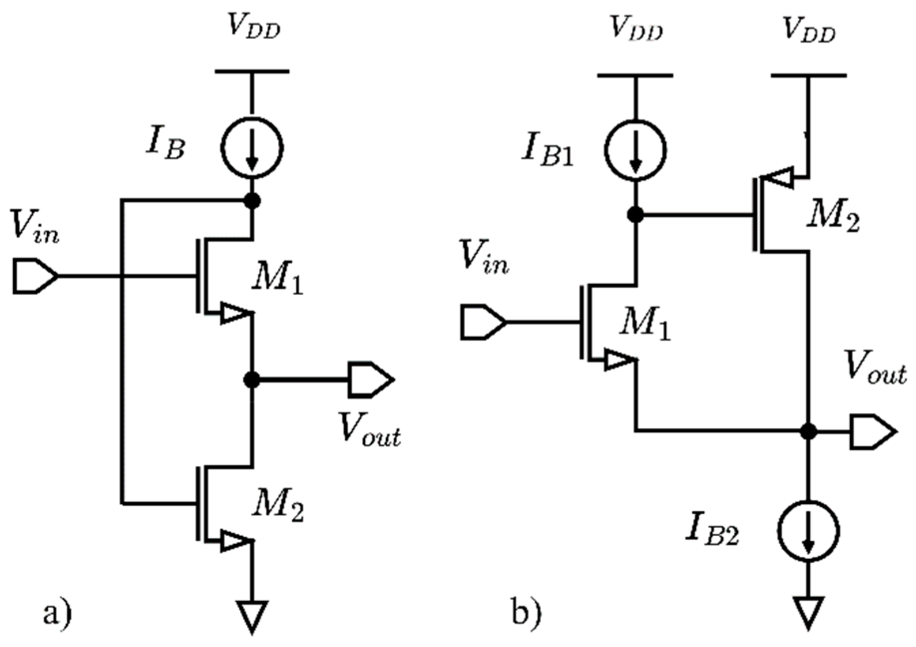
Figure 2.
SSF-C biquads with NMOS (a) and PMOS (b) input devices.
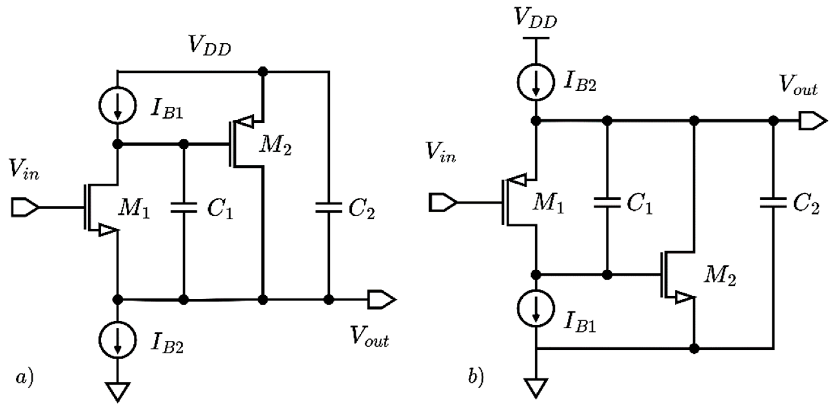
Figure 3.
Small-signal circuit of the proposed biquad.
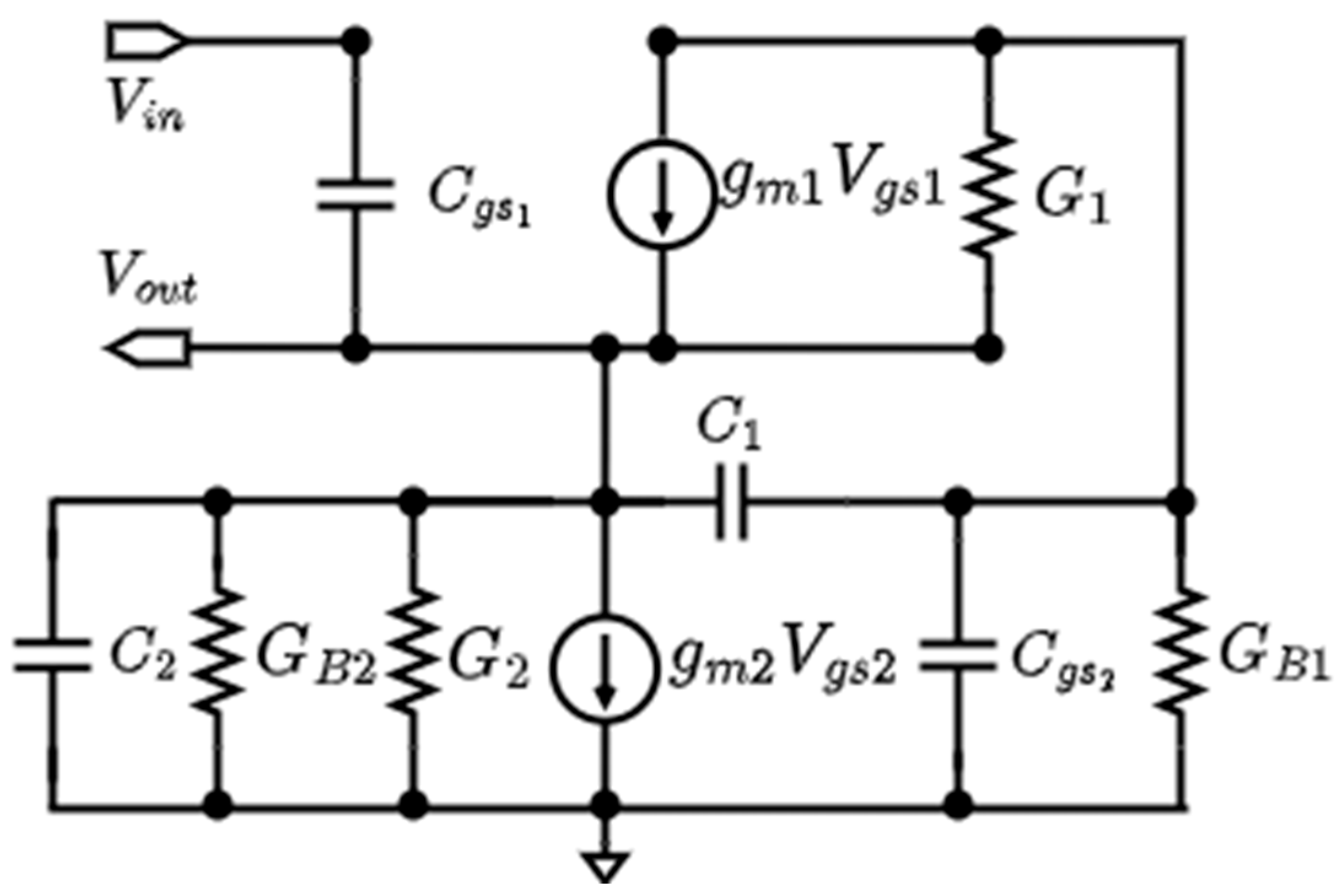
Figure 4.
Small-signal equivalent circuit for noise analysis.
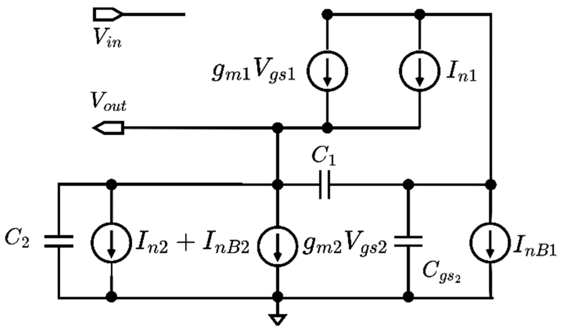
Figure 5.
4-th order filter with cascaded N-type and P-type biquads.
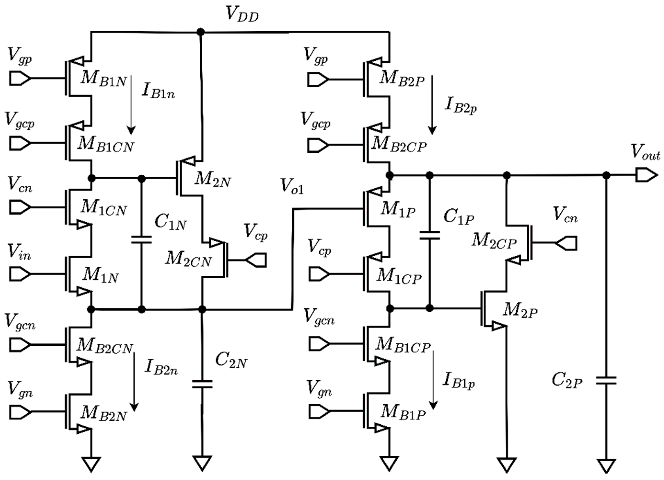
Figure 6.
Layout of (a) N-type, and (b) P-type biquads.
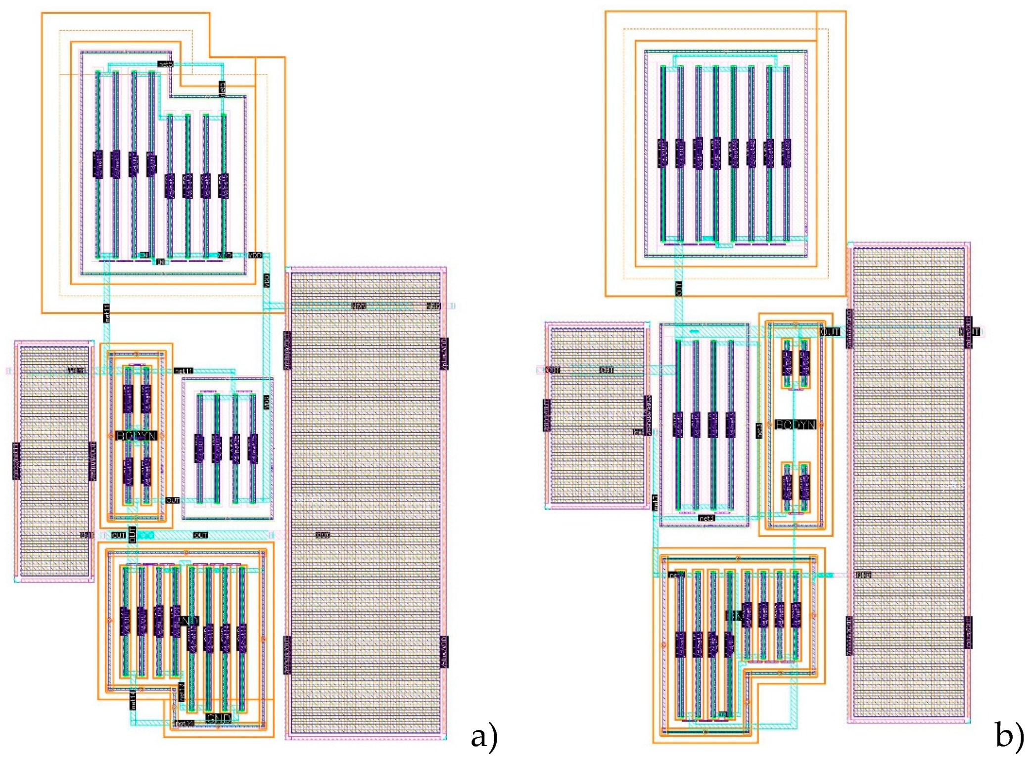
Figure 7.
Frequency response of the N-type, P-type and cascaded (N + P) filters.
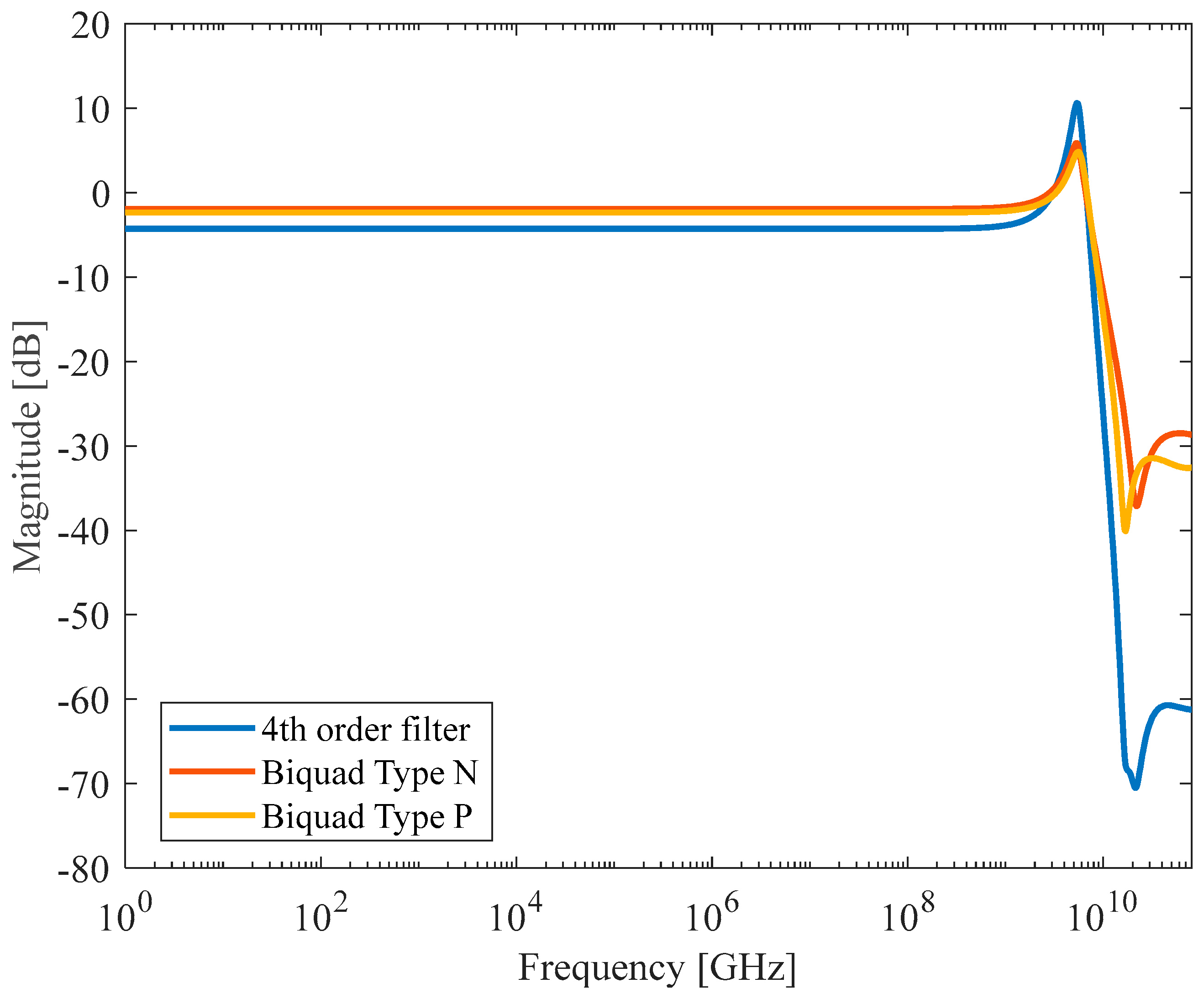
Figure 8.
Tuning of resonance frequency for (a) N-type and (b) P-type biquads.
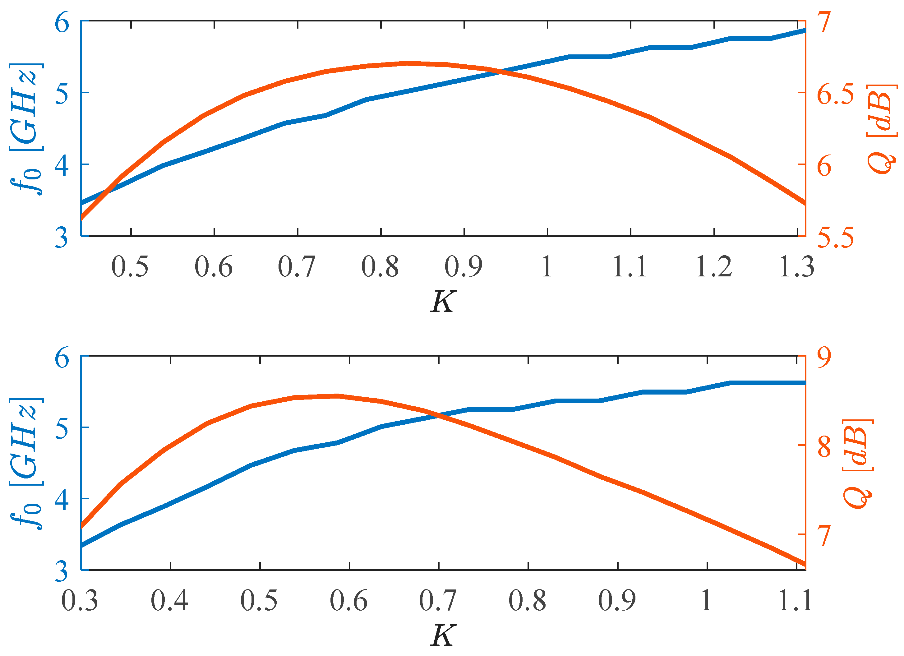
Figure 9.
Tuning of quality factor for (a) N-type and (b) P-type biquads.
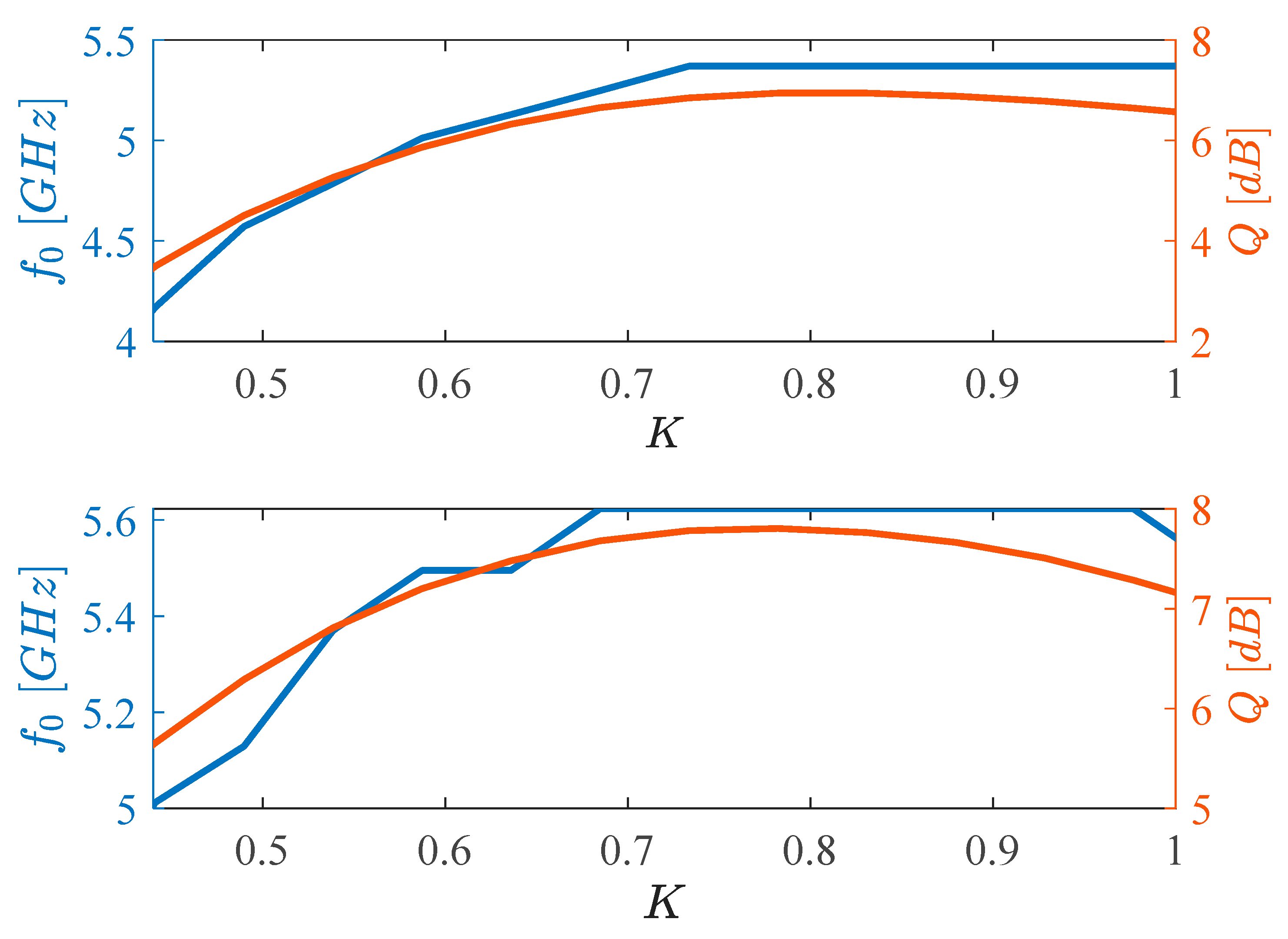
Figure 10.
Output noise spectra for N-type and P-type biquads.
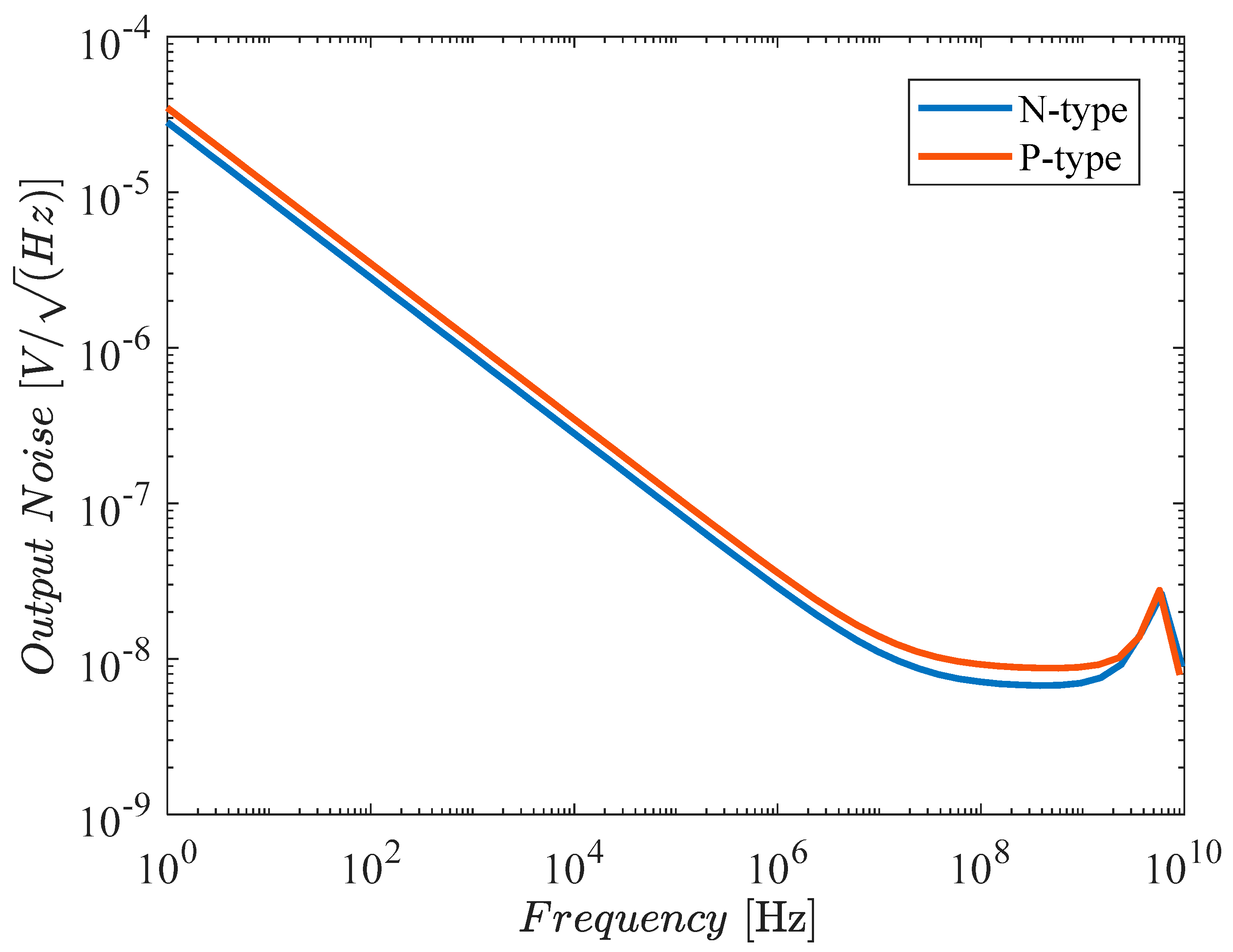
Figure 11.
DC transcharacteristic for N-type and P-type biquads.
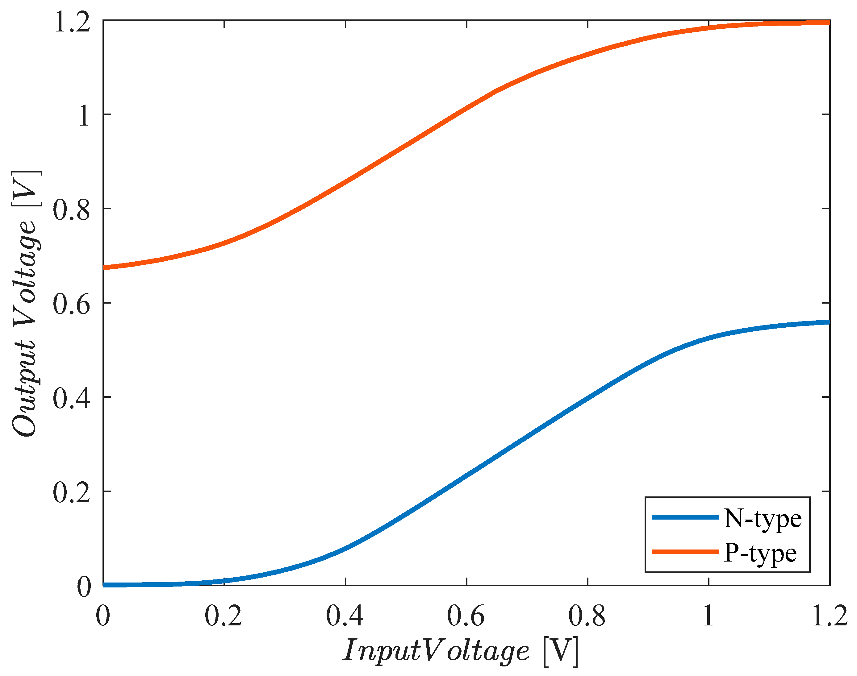
Figure 12.
Two-tone spectra of the (a) N-type and (b) P-type biquads for 900MHz and 1GHz 200mVpp inputs.
Figure 12.
Two-tone spectra of the (a) N-type and (b) P-type biquads for 900MHz and 1GHz 200mVpp inputs.
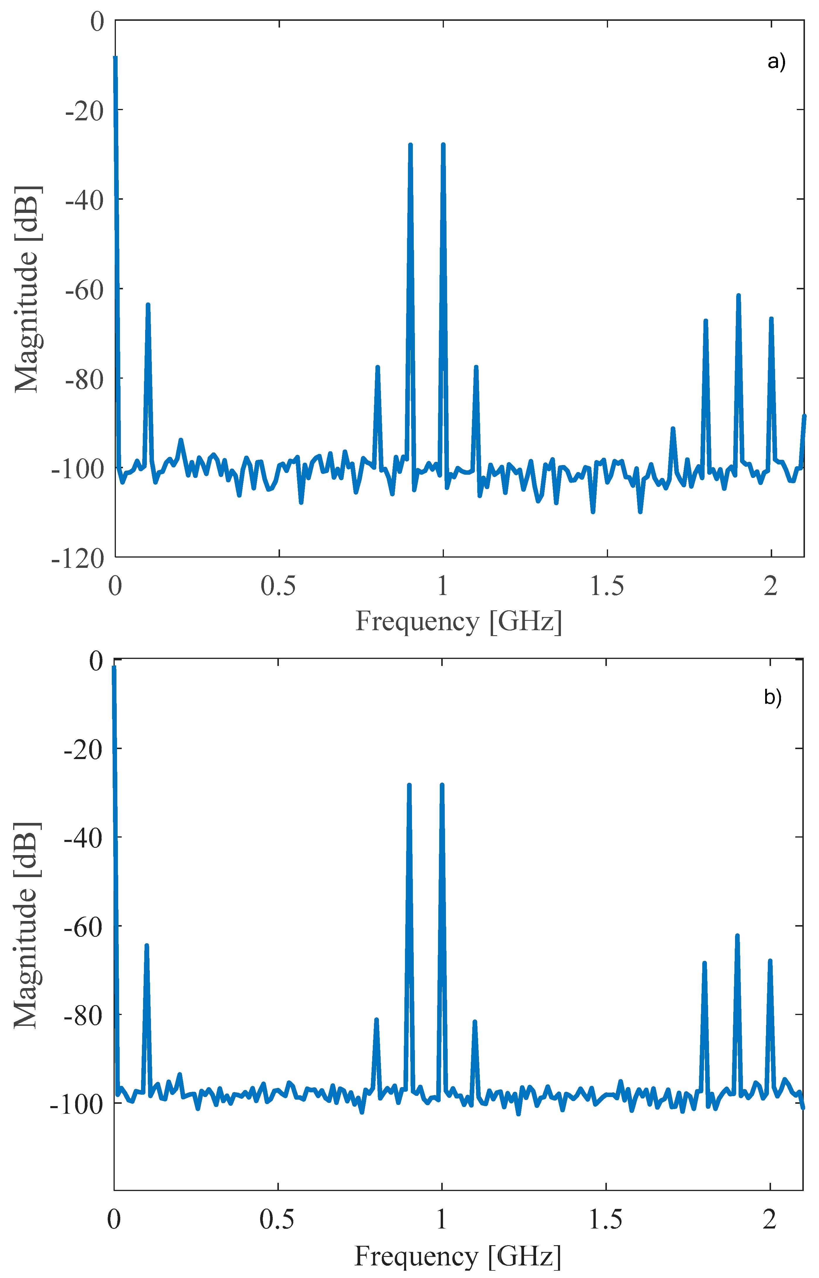

Table 1.
Device sizing.
| N-type biquad | P-type biquad | Units | |
| WM1, WM1C | 4.4 | 11.2 | μm |
| WM2, WM2C | 7.6 | 3.2 | μm |
| WMB1, WMB1C | 5.5 | 5 | μm |
| WMB2, WMB2C | 10 | 12 | μm |
| IB1 | 300 | 350 | μA |
| IB2 | 700 | 700 | μA |
| C1 | 50 | 40 | fF |
| C2 | 90 | 80 | fF |
Table 2.
Performance of N-type biquad under supply and temperature variations.
| Performance | Nominal | VDD + 10% | VDD - 10% | 0°C | 80°C |
| f0 [GHz] | 5.4 | 5.2 | 5.4 | 5.6 | 5 |
| f3dB [GHz] | 8.1 | 7.9 | 8.1 | 8.3 | 7.5 |
| Q [dB] | 6.6 | 5.6 | 6.5 | 6.7 | 6 |
| A0 [dB] | -1.9 | -2 | -1.9 | -1.9 | -2 |
| Pdiss [mW] | 0.82 | 0.82 | 0.82 | 0.81 | 0.83 |
Table 3.
Performance of P-type biquad under supply and temperature variations.
| Performance | Nominal | VDD + 10% | VDD - 10% | 0°C | 80°C |
| f0 [GHz] | 5.5 | 4.9 | 5.9 | 5.6 | 5.3 |
| f3dB [GHz] | 7.9 | 7.1 | 8.3 | 8 | 7.5 |
| Q [dB] | 7.2 | 5.6 | 8.1 | 7.3 | 6.6 |
| A0 [dB] | -2.3 | -2.3 | -2.3 | -2.3 | -2.4 |
| Pdiss [mW] | 0.67 | 0.57 | 0.74 | 0.66 | 0.70 |
Table 4.
Monte Carlo process and mismatch simulations.
| Performance | N-type biquad | P-type biquad | ||
| Mean | Std | Mean | Std | |
| f0 [GHz] | 5.6 | 0.186 | 5.5 | 0.177 |
| f3dB [GHz] | 8 | 0.223 | 7.8 | 0.224 |
| Q [dB] | 6.5 | 0.48 | 7 | 0.58 |
Table 5.
Comparison with the literature.
| Performance | This work | [34] | [28] | [39] | [16] | [40] | [23] | [13] | [12] | ||
| N-type | P-type | N-type | P-type | ||||||||
| Tech. [nm] | CMOS 28 FDSOI | CMOS 28 FDSOI | BICMOS | CMOS 22 | BICMOS | CMOS 90 | BICMOS | CMOS 28 | CMOS 22 | ||
| Npole | 2 | 2 | 2 | 2 | 2 | 5 | 6 | 4 | 2 | 5 | 3 |
| VDD [V] | 1.2 | 1.2 | 1.2 | 1.2 | 2.7 | 0.8 | 3 | 1 | 3 | 1.1 | 1.4 |
| Pdiss [mW] | 0.82 | 0.67 | 1.08 | 1.6 | 15.75 | 19.9 | 43 | 3.7 | 18 | 30 | 140 |
| f3dB [GHz] | 8.1 | 7.9 | 7.57 | 7.2 | 17.1 | 4.9 | 10.3 | 1 | 9.55 | 3.3 | 10 |
| A0 [dB] | -1.9 | -2.3 | -1.6 | -1.8 | 3.8 | 0.5 | -0.2 | 0 | -0.5 | -1 | 1.3 |
| Pinoise [dBm] | -44.7 | -45.4 | -43.5 | -39.4 | -50.4 | -56.8 | -45.9 | -46 | -46.8 | -56 | -55.6 |
| [dBm] | -10 | -10 | -10 | -10 | -2.9 | -1 | -13 | -1 | -17 | -10.6 | |
| -33.1 | -33.4 | -46.8 | -42.4 | -51.7 | -42.6 | -41.77 | -64 | -40 | -45 | ||
| IIP3 [dBm] | 17.25 | 5.5 | |||||||||
| DR [dB] | 33.9 | 34.4 | 40.2 | 35.9 | 47.9 | 41.7 | 43.1 | 34.9 | 50.9 | 38.4 | 44 |
| Area [mm2] | 0.00038 | 0.00038 | 0.000246 | 0.000193 | 0.0025 | 0.05 | 0.02 | 0.000092 | 0.0027 | 0.09 | 0.01 |
| Area/pole [mm2] | 0.00019 | 0.00019 | 0.000123 | 0.000096 | 0.00125 | 0.01 | 0.003 | 0.000023 | 0.00135 | 0.018 | 0.003 |
| FOM1 [mW] | 0.41 | 0.33 | 0.54 | 0.3 | 7.87 | 3.98 | 7.2 | 0.925 | 9 | 6 | 46.7 |
| FOM2 [pW/Hz] | 0.051 | 0.042 | 0.071 | 0.042 | 0.461 | 0.812 | 0.696 | 0.925 | 0.942 | 1.818 | 4.667 |
| FOM3 [aW/Hz] | 20.52 | 15.31. | 6.82 | 10.78 | 7.48 | 54.88 | 33.84 | 297.46 | 7.65 | 267.08 | 185.93 |
| Sin. /Meas. | S | S | S | S | S | M | S | S | S | M | M |
Disclaimer/Publisher’s Note: The statements, opinions and data contained in all publications are solely those of the individual author(s) and contributor(s) and not of MDPI and/or the editor(s). MDPI and/or the editor(s) disclaim responsibility for any injury to people or property resulting from any ideas, methods, instructions or products referred to in the content. |
© 2025 by the authors. Licensee MDPI, Basel, Switzerland. This article is an open access article distributed under the terms and conditions of the Creative Commons Attribution (CC BY) license (http://creativecommons.org/licenses/by/4.0/).
Copyright: This open access article is published under a Creative Commons CC BY 4.0 license, which permit the free download, distribution, and reuse, provided that the author and preprint are cited in any reuse.


