
Submitted:
25 March 2025
Posted:
25 March 2025
You are already at the latest version
Abstract
In this study, we developed core system software for a microcontroller-based, low-cost data acquisition system, along with the necessary environmental software. The system includes an analog-to-digital converter, digital inputs/outputs, pulse-width modulation, and a counter, supporting data transmission via USB 2.0 full-speed. We also designed flexible and easily configurable firmware to enable synchronization with external devices, making the system highly adaptable for applications such as laboratory research setups or scientific instrumentation. We created the schematic and printed circuit board for the core system, which is based on a 32-bit ARM Cortex-M4F microcontroller. In addition, we measure the signal-to-noise and distortion of the analog-to-digital converter to evaluate its conversion capability.
Keywords:
data acquisition device
; analog to digital converter
; effective number of bits
1. Introduction
Measurement instruments need to convert analog signals obtained from the desired physical phenomenon into a digital representation for processing in digital computer systems [1,2]. A data acquisition (DAQ) device is a critical (customized) tool for achieving this task. Many manufacturers offer various general-purpose DAQ solutions for specific applications in the market, most of which are expensive. The advanced ones include various components that are analog to digital converter (ADC), digital to analog converter (DAC), digital inputs/outputs (I/O), counter, pulse width modulation (PWM) etc. The low- and mid-level DAQ systems are generally based on microcontrollers [3,4,5,6,7,8,9,10,11,12,13,14], while high-speed DAQ systems [15,16] use FPGAs (field programmable gate array) with advanced ADC, DAC, and synchronous dynamic random-access memory (SDRAM) chips that provide parallel communication with the FPGA, and they are mostly sold at high prices.
Developing individual data acquisition system solutions for a specific task is essential to eliminate unnecessary electronics, thereby reducing both cost and size. Several low-cost data acquisition devices have been developed, typically based on microcontroller (−C). Most of these devices are designed for various specific tasks, such as applications in the automotive industry [3,4,5], air quality measurement [6], electrocardiogram measurement [7], rotordynamic data collection [8], and test equipment [9], while others are designed for general-purpose applications [10,11,12,13,14].
A significant amount of work utilizes serial communication which limits the data transfer speed between the −C and PC. One study presents a low-cost, general-purpose DAQ system that supports USB (Universal Serial Bus) 2.0 communication, based on a PIC −C [14]. The virtual instrument (VI) library for LabVIEW is well-developed. However, the RAM size of the −C restricts the buffer size to a maximum of 1024 samples. The maximum sampling frequency is 100 KSa/s, and it supports only single-ended analog inputs and does not allow simultaneous data conversion across multiple analog input channels. Furthermore, it lacks built-in signal conditioning hardware.
In this work, we develop embedded software for a 32-bit ARM Cortex-M4F-based microcontroller to create a general-purpose real-time DAQ system. The system includes a 4-channel, 12-bit analog to digital converter, 4-channel digital I/Os, a 32-bit counter, pulse width modulation signal generator, and synchronization wires for peripheral (or external) devices. It also supports USB 2.0 full-speed communication. To ensure low cost, our focus is solely on software development for a general-purpose DAQ system, providing access to all possible features of the microcontroller hardware. We develop the required software environment to control the DAQ device for Python and LabVIEW on the PC side. The DAQ system is tested using the Tiva C Series TM4C123G LaunchPad Evaluation Board, produced by Texas Instruments Inc. [17], which is priced at approximately $17. In addition, we design the schematic and printed circuit board (PCB) for the core board of the DAQ system based on the TM4C123GH6PM microcontroller. The external electronics for signal conditioning circuit, such as level shifters and amplifiers, can be easily integrated into the core board as needed.
2. Materials and Methods
In this study, we use Tiva C Series TM4C123G LaunchPad Evaluation Board for firmware developing process. It has onboard programmer to write compiled program (as a .hex file) to microcontroller.
The has a 32-bit ARM Cortex-M4F processor with a built-in floating-point unit. It can run at speeds up to 80 MHz, making it suitable for real-time signal processing tasks. It includes 32 KB of SRAM for data storage, 256 KB of flash memory for program code, and 2 KB of EEPROM for non-volatile data storage. It supports the USB 2.0 full-speed communication that we use bulk transfer type to data transmission.
The TM4C123GH6PM microcontroller includes major hardware components for developing modern data acquisition systems. It features general-purpose input/output (GPIO) pins that can be assigned to specific tasks such as analog-to-digital conversion, digital input/output, pulse-width modulation, or counting, provided the hardware of the pin supports it. Now, we introduce the major components of the designed integrable core system for data acquisition devices.
2.1. Analog to Digital Converter
The analog to digital converter is major component of the data acquisition systems for converting analog signal, such as sensor outputs, to digital information defined as bit array. The number of bits in the digital output defines the precision of the conversion and is known as the resolution. For example, a 12-bit ADC can represent an analog signal using discrete levels. The number of samples acquired per second defines the sampling rate, expressed in samples per second (). This parameter determines how quickly the ADC can process continuous analog signals. The number of samples acquired during a conversion cycle without interruption denotes the memory depth or buffer size, which is generally limited by the RAM size of the microcontroller.
The TM4C123GH6PM microcontroller has two independent ADC modules, ADC0 and ADC1, each utilizing a successive approximate register (SAR) architecture and capable of operating concurrently without interference [18]. The ADC0 module is configured to process analog input channels AIN0, AIN1, AIN2, and AIN3, which are mapped to GPIO pins PE3, PE2, PE5, and PE4, respectively, in a single-ended sampling configuration. For applications requiring enhanced noise immunity or differential signal processing, the ADC0 module supports differential sampling configurations. In this mode, the pin pairs PE3 and PE2 serve as the DIFF0+ and DIFF0- inputs, while PE5 and PE4 function as the DIFF1+ and DIFF1- inputs. This dual-configuration capability makes the ADC highly versatile for a wide range of analog signal acquisition tasks. In our core-system software, we support both single-ended and differential input configurations.
2.2. Digital Inputs and Outputs
Another important component of the DAQ systems is the digital inputs and outputs. The GPIO pins of the −C can be configured as digital inputs or outputs. A digital input reads the logic state (high or low) of an external digital signal, such as from a switch or sensor, while a digital output sets a pin to a logic high or low state to control devices like LEDs, relays, and other peripherals. The four GPIO pins PB0, PB1, PB2, and PB3 can be configured as digital I/O, corresponding to D0, D1, D2, and D3, respectively.
2.3. Counter and Pulse Width Modulation
The −C includes counter hardware that can count external events. The counter can be operated in different modes, such as one-shot or periodic, and are useful for timing, frequency measurement, and event counting applications. We use 32-bit wide timer counting the signals for rising, falling, and both edges, which the pin PC4 pin assigned to CNT0.
Another component is pulse-width modulation, a technique that controls power delivery by varying the width of on-off pulses in a signal. The PC4 pin (M0PWM6) also supports generating a pulse-width modulation signal, controlled by Module 0 PWM Generator 3 of the microcontroller.
3. Results
We first generate the firmware for the −C using TivaWare peripheral driver library in Code Composer Studio [19]. Then, we develop the necessary software environments, such as packages and user interfaces (UI), to control −C functions, receive data, and visualize it on the PC.
We set the clock frequency of the −C to 80 MHz and allocate 20 KB of SRAM for the ADC sampling buffer, supporting up to 10 KSa of memory depth. The DAQ system we designed supports 12-bit ADC signal conversion, can be configured four channel single-ended input or a two channel differential input. It also includes four digital input/output channels, PWM, and a 32-bit counter. The main architecture of the core system, shown in Figure 1, was developed through the following steps.
3.1. Firmware Development
In this section, we develop all components of the firmware for the real-time data acquisition system. A command-driven software structure is created to execute the relevant task for each user command received. The user commands configure the analog-to-digital converter, digital inputs/outputs, PWM and the counter components of the DAQ system as follows:
Analog to digital conversion: The presented design supports four single-ended (SE) channels and two differential (DIFF) channels for real-time analog-to-digital conversion. The sampling rate can be configured up to 1 MSa/s through user commands received from the PC. The sample depth for the 12-bit ADC is set to 10 KSa, which enables wide-range signal acquisition and visualization. The DAQ system also supports the simultaneous multi-channel acquisition.
The bandwidth of the analog inputs is theoretically limited by the Nyquist frequency (500 MHz). However, in high-accuracy applications, it is common to sample at 5–10 times the highest signal frequency, meaning the practical bandwidth is closer to 100 KHz.
We design advanced clock configuration for DAQ system. The ADC clock source can be configured as either internal (onboard) or external. To generate an internal (onboard) clock source for the ADC sampling rate, PWM1_BASE of −C is used. Thus, the sampling rate can be set in the range of 10 KSa/s to 1 MSa/s and can be monitored from pin PA6. For providing the external ADC clock source, the square signal can be applied the PB4 pin of the −C up to 1 MSa/s.
The trigger source to start a complete analog-to-digital conversion cycle can be configured to be initiated by either software or hardware. To start a cycle via software, the user sends a ADC:CAPTure command, while hardware triggering is performed by applying a pulse to PF4. Moreover, the PF3 pin can be configured as a receive trigger output, toggling from high to low when a cycle is completed.
Considering the above flexible clock and trigger configurations, the DAQ device can synchronize with external clock sources and devices, such as lock-in amplifiers.
Digital inputs/outputs: The four pins (D0, D1, D2, and D3) of the microcontroller can be configured as digital inputs or outputs and can operate in parallel. The rise/fall time of the digital pins is up to [18].
Counter and PWM: The PC4 pin is configured as a 32-bit counter and can be programmed to count the rising edge, falling edge, or both edges of the input signal. It supports capturing a minimum pulse width of 10 ns for signals up to 5 MHz. Additionally, the PC4 pin can be programmed as a PWM source, with the frequency controlled by a 16-bit counter defined as , where . Both the frequency and duty cycle of the PWM can also be configured via user commands.
Command set: The data acquisition system supports the SCPI (Standard Commands for Programmable Instruments) command standard [20]. The command syntax is defined as ADC:SAMPling:RATE <rate>, which is used to set the sampling rate of the analog-to-digital converter. For example, you can use commands like ADC:SAMPling:RATE 1000000 or its abbreviated form, ADC:SAMP:RATE 1000000, to set the sampling rate to 1 MSa/s.
3.2. Hardware Development
We use a low-cost development kit named Tiva C Series TM4C123G LaunchPad Evaluation Board [17]. In addition, we create a schematic design for a core board based on the TM4C123GH6PM microcontroller (sells for approx. $10) for DAQ system hardware, as shown in Figure 2a). We produced the PCB of core-board shown in Figure 2b) (left), along with its pin diagram (right). It includes all necessary pin assignments to support the features of the developed firmware and can be integrated with external circuits, such as signal conditioning modules (e.g., amplifiers, level shifters).
3.3. User Interface Development
On the PC side, we develop two solutions for managing the data acquisition device. First, we create Python code using the Virtual Instrument Software Architecture (VISA) library, allowing the user to access all functions of the DAQ device via SCPI commands. We also create a user interface program, as shown in Figure 3, where the user can collect data from the ADC channels and apply triggers to visualize the signal form, similar to digital storage oscilloscopes.
Second, we develop the VI (Virtual Instrument) package for LabVIEW which includes to required VI components, shown in Figure 4, to access and control all functions of the data acquisition device. We create an example VI to collect data from analog channels, with the front panel and block diagram of VI shown in Figure 5 and Figure 6, respectively.
3.4. Device Driver
Our design uses a USB interface with a host-device configuration to send data to the PC program and receive user SCPI commands. It supports USB 2.0 full-speed (12 Mb/s), enabling fast data transfer to the PC.
The setup information (.inf) file for the DAQ device driver is generated using the NI-VISA Driver Wizard [21] for integration with the VISA framework. We generate LabVIEW and Python programs that use VISA and PyVISA libraries, respectively. In an addition, we test libUSB-win32 INF Wizard to create .inf file for compatibility with the open source USB driver library named as libusb [22] driver stack as an alternative to NI-VISA. Data transmission is handled via the PyUSB library, which interfaces directly with the USB device through libusb. Both driver configurations were successfully validated, demonstrating reliable communication and data transfer functionality.
3.5. Signal to Noise and Distortion
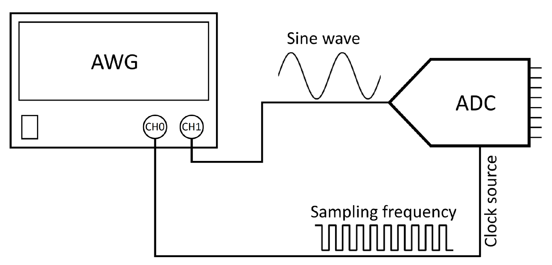
Lastly, we evaluate the dynamic performance of the ADC component in the target data acquisition system using the signal-to-noise and distortion (SINAD) measurement technique [23]. The SINAD measurement accounts for several factors, including quantization noise, clock jitter, analog noise, and total harmonic distortion [24]. In this technique, arbitrary waveform generator (AWG) generates a sine wave at a known frequency. Then, the sine wave digitized with using ADC of the DAQ system. Since the AWG and DAQ are two separate devices driven by different clock sources, external influences (temperature etc.) on the clock signals may introduce unique distortions in each device. This means that the measurement accuracy may decrease due to spectral leakage [25]. One practical way to avoiding spectral leakage, both the ADC and the AWG to be driven by the same clock source. Such a clock sharing provides coherent sampling [23,26].
To achieve coherent sampling in our SINAD measurement setup, the analog-to-digital converter is driven by a 1 MHz clock signal sourced from Channel 0 (CH0) of the arbitrary waveform generator, as illustrated in Figure 7. The core-system of DAQ device developed in this study is specifically designed to support such a configuration. By synchronizing the sampling frequency of ADC with the clock source of AWG, any frequency drift or error originating from the signal generator is inherently mirrored in the sampling process. This synchronization effectively eliminates discrepancies, ensuring that the frequency of the input signal consistently remains an integer multiple of the frequency resolution, even in the presence of clock drift.
A sine wave at a frequency of with an amplitude of and an offset of is generated on Channel 1 (CH1) of the AWG. It is then digitized by the AI0 channel of the DAQ system for SINAD measurement. The setup for coherent sampling, shown in Figure 7, only allows a single-ended input configuration for the ADC. A band-pass filter is applied to the signal as a pre-processing technique to reduce noise and improve measurement accuracy. The SINAD value, expressed in decibels (dB), can be calculated from the digitized sine waveform using the LabVIEW SINAD Analyzer.vi tool and was measured to be dB. Additionally, the SINAD value for the single-ended input of the ADC is specified as a typical value of 63 dB in the datasheet of the microcontroller [18]. Thus, we compared our measured value with this specification and confirmed the accuracy of our results.
On the other hand, the effective number of bits (ENOB) is a measure of the actual resolution of an analog-to-digital converter (ADC), reflecting its analog-to-digital conversion capability [23]. It can be calculated using the SINAD value with the formula given as [27,28]. By applying this formula, we calculate the ENOB to be approximately bits.
4. Conclusions
In conclusion, we have developed a cost-effective, multifunctional core system for a data acquisition device based on the TM4C123GH6PM microcontroller. We created a software environment on the PC side that supports Python and LabVIEW. The system has a flexible structure, making it suitable for teaching and research laboratories. It supports analog-to-digital conversion with simultaneous multi-channel operation, digital input/output, PWM, and counter tasks. It is also useful for advanced tasks, such as synchronization with external devices, with signal bandwidths up to 100 kHz. We use USB 2.0 full-speed communication to control all functions of the DAQ system and enable data transmission.
We create a schematic design, and also build the PCB for the core-system that can be upgraded for specific tasks with needed external electronics for signal conditioning circuits.
Lastly, we measure the signal-to-noise and distortion ratio and calculate the effective number of bits to evaluate the dynamic range of an analog-to-digital converter. We obtain the similar dynamics given the data sheet of the analog to digital converter [18].
Such a core system for data acquisition can be integrated into specialized devices, such as scientific instruments, industrial measurement equipment, and control systems, providing an onboard and cost-effective solution. Its compact design and flexibility enable seamless incorporation into embedded platforms, allowing real-time data acquisition and communication without the need for bulky or expensive external hardware.
Acknowledgments
E. E. and S.Ç. acknowledge support from the Scientific and Technological Research Council of Turkey (TÜBİTAK) Grant No. 1919B012316038.
Appendix A Pin Configuration
The developed integrable core system for data acquisition devices, based on the TM4C123GH6PM microcontroller, includes analog inputs, digital inputs/outputs, pulse-width modulation, a 32-bit counter, and synchronization wires. It also operates on the Tiva C Series TM4C123G LaunchPad Evaluation Board, with the pin assignments provided in Table A1.

Table A1.
Pin assignments of the developed DAQ system.
| Specification | Pin |
|---|---|
| Analog Inputs | |
| • AI0/SE or AI0+/DIFF | PE3 |
| • AI1/SE or AI0-/DIFF | PE2 |
| • AI2/SE or AI1+/DIFF | PE5 |
| • AI3/SE or AI1-/DIFF | PE4 |
| Digital I/Os | |
| • D0 | PB0 |
| • D1 | PB1 |
| • D2 | PB2 |
| • D3 | PB3 |
| Counter and PWM | |
| • CNT0 or PWM | PC4 |
| Synchronization Wires | |
| • ADC Clock In | PB4 (Up to 1 MHz) |
| • ADC Trigger In | PF4 |
| • ADC Event Trigger Out | PF3 |
| Test Signal | |
| • 10 KHz %25 Duty Cycle | PB6 |
References
- Park, J.; Mackay, S. Practical Data Acquisition for Instrumentation and Control Systems; Newnes Elsevier: Oxford, 2003. [Google Scholar]
- Emilio, M.D.P. Data Acquisition Systems: From Fundamentals to Applied Design; Springer New York: New York, NY, 2013. [Google Scholar]
- González, A.; Olazagoitia, J.; Vinolas, J. A Low-Cost Data Acquisition System for Automobile Dynamics Applications. Sensors 2018, 18, 366. [Google Scholar] [CrossRef] [PubMed]
- Singh, H.P.; Singh, R. Low Cost Data Acquisition System for Road-Vehicle Interaction Using Arduino Board. J. Phys.: Conf. Ser. 2021, 1831, 012031. [Google Scholar]
- Shalgar, S.; Bindu, R. Design and Development of a Novel Multichannel Data Acquisition System Using Labview for an Automobile Air Conditioning Application. Journal of Thermal Engineering 2022, 8, 14–28. [Google Scholar] [CrossRef]
- Carre, A.; Williamson, T. Design and Validation of a Low Cost Indoor Environment Quality Data Logger. Energy and Buildings 2018, 158, 1751–1761. [Google Scholar]
- Gupta, R.; Bera, J.; Mitra, M. Development of an Embedded System and MATLAB-Based GUI for Online Acquisition and Analysis of ECG Signal. Measurement 2010, 43, 1119–1126. [Google Scholar]
- Pellegrino, G. Design of a Low-Cost Data Acquisition System for Rotordynamic Data Collection. PhD thesis, California Polytechnic State University, 2019. (Thesis).
- Atcı, A.; Ünal, E.; Akgöl, O. A Low-Cost Data Acquisition System Design for Multifunctional Test Equipment in Electronics Laboratories. Electronics 2024, 13, 4937. [Google Scholar] [CrossRef]
- Martín, F.F.; Llopis, M.V.; Rodríguez, J.C.; González, J.B.; Blanco, J.M. Low-cost Open-source Multifunction Data Acquisition System for Accurate Measurements. Measurement 2014, 55, 265–271. [Google Scholar] [CrossRef]
- Katrancıoğlu, S.; Savaş, K.; Erdal, H. A Modular and Low-Cost Data Acquisition Card Design with Multitasking Support. Procedia - Social and Behavioral Sciences 2010, 2, 5266–5270. [Google Scholar]
- Perçin, F.; Sahin, S.; Gökçen, A. Low-Cost MATLAB-Simulink Compatible Data Acquisition Card Hardware and Software Design for Control and Test Applications. Avrupa Bilim Ve Teknoloji Dergisi 2022, 37, 156–160. [Google Scholar]
- Seo, S.; Park, Y.; Lee, Y. Development of a Cost-effective Data Acquisition System Using an Open-source Hardware and Matlab/Simulink. In Proceedings of the Proceedings of the 13th International Conference on Informatics in Control, Automation and Robotics, Lisbon, Portugal, 2016; pp. 484–491.
- Hercog, D.; Gergič, B. A Flexible Microcontroller-Based Data Acquisition Device. Sensors 2014, 14, 9755–9775. [Google Scholar] [CrossRef] [PubMed]
- Kandadai, V.; Sridharan, M.; Parvathy, S.M.; Pitchaimuthu, R. A Comprehensive Embedded Solution for Data Acquisition and Communication Using FPGA. Journal of Applied Research and Technology 2017, 15, 45–53. [Google Scholar] [CrossRef]
- Wang, Y.; Zhang, M.; Ji, S.; Wang, J. Design of Multi-channel Real-time Signal Acquisition System. J. Phys.: Conf. Ser. 2022, 2189, 012007. [Google Scholar] [CrossRef]
- Texas Instruments Inc.. TM4C123G LaunchPad Evaluation Kit. Available: https://www.ti.com/tool/EK-TM4C123GXL (Accessed March 23, 2025).
- Texas Instruments Inc.. Tiva TM4C123GH6PM Microcontroller Data Sheet. Available: https://www.ti.com/lit/gpn/tm4c123gh6pm (Accessed March 23, 2025).
- Texas Instruments Inc.. TivaWare Peripheral Driver Library User’s Guide. Available: https://www.ti.com/lit/pdf/spmu298 (Accessed March 23, 2025).
- European SCPI Consortium. Standard Commands for Programmable Instruments (SCPI). Available: http://www.ivifoundation.org/downloads/SCPI/scpi-99.pdf (Accessed March 24, 2025).
- National Instrument Corp.. NI-VISA Driver Wizard Overview. Available: https://www.ni.com/docs/en-US/bundle/ni-visa-api-ref/page/ni-visa-api-ref/overview.html (Accessed March 23, 2025).
- libusb. A Cross-platform User Library to Access USB Devices. Available: https://libusb.info/ (Accessed March 23, 2025).
- IEEE Standard for Terminology and Test Methods for Analog-to-Digital Converters, 2011. pp. 1–139.
- Edwards, S.D. Edwards, S.D. Effective Number of Bits Calculator User’s Guide, Maxim Integrated. Available: https://www.hpcalc.org/details/7339 (Accessed March 23, 2025).
- Peng, X.; Li, J.; Zhang, D.; Hu, C.; Sun, N.; Jiang, J. High-Precision ADC Spectrum Testing under Non-Coherent Sampling Conditions. Sensors 2022, 22, 8170. [Google Scholar] [CrossRef] [PubMed]
- Zhuang, Y.; Chen, D. ADC Spectral Testing with Signal Amplitude Drift and Simultaneous Non-coherent Sampling. J Electron Test 2017, 33, 305–313. [Google Scholar]
- Zheng, Y.; Zhao, Y.; Zhou, N.; Wang, H.; Jiang, D. A Short Review of Some Analog-to-Digital Converters Resolution Enhancement Methods. Measurement 2021, 180, 109554. [Google Scholar]
- Kay, A.; Green, T. Kay, A.; Green, T. Analog Engineer’s Pocket Reference, Texas Instruments Incorporated, 2019. Available: https://www.ti.com/lit/SLYW038C (Accessed March 23, 2025).
Figure 1.
An overview of the main components of the software architecture for the data acquisition system.
Figure 1.
An overview of the main components of the software architecture for the data acquisition system.
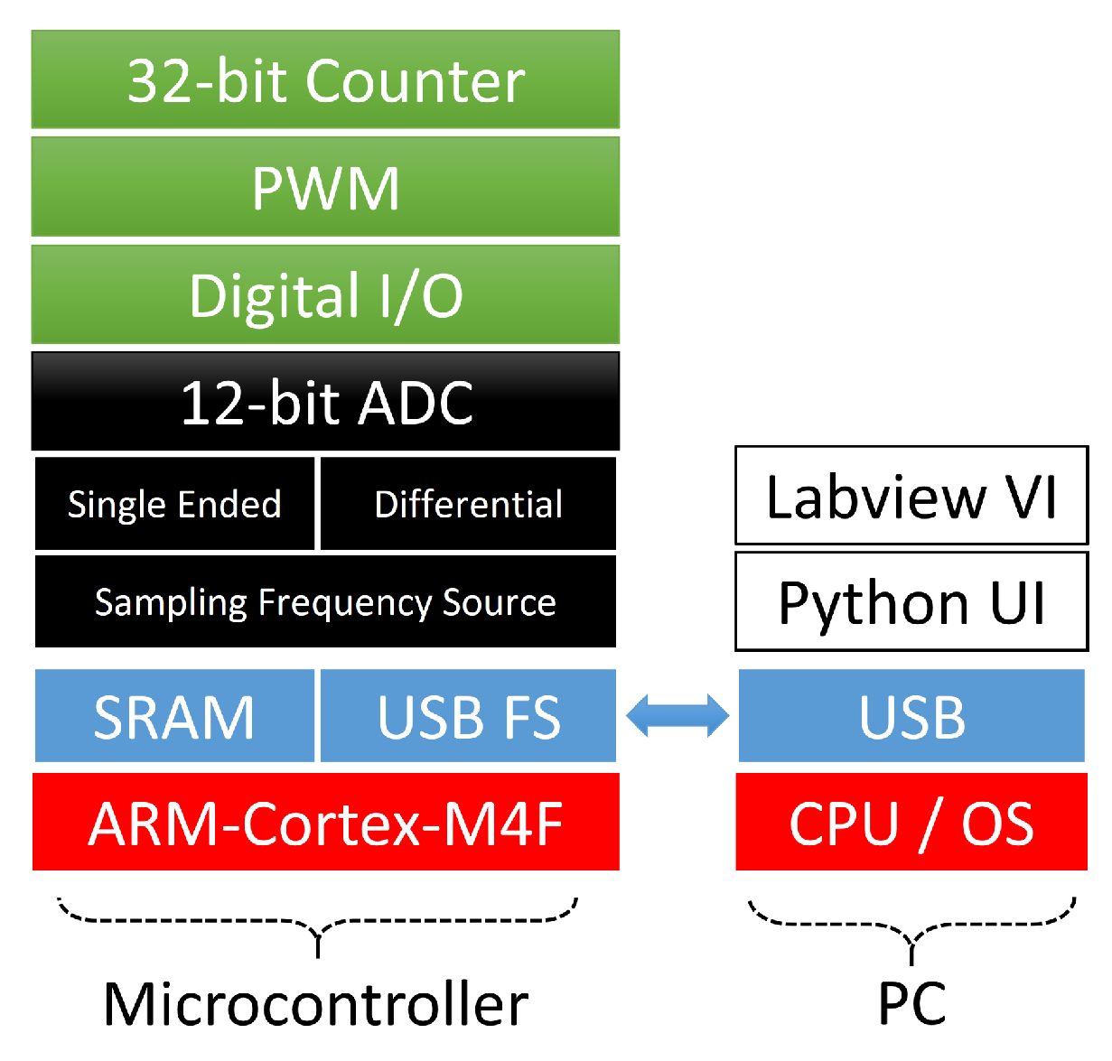
Figure 2.
a) Schematic design and b) generic view of the PCB (left) with the pin diagram (right) of the core board for data acquisition system. The pin assignments for the Tiva C Series TM4C123G LaunchPad Evaluation Board are given in Appendix A.
Figure 2.
a) Schematic design and b) generic view of the PCB (left) with the pin diagram (right) of the core board for data acquisition system. The pin assignments for the Tiva C Series TM4C123G LaunchPad Evaluation Board are given in Appendix A.
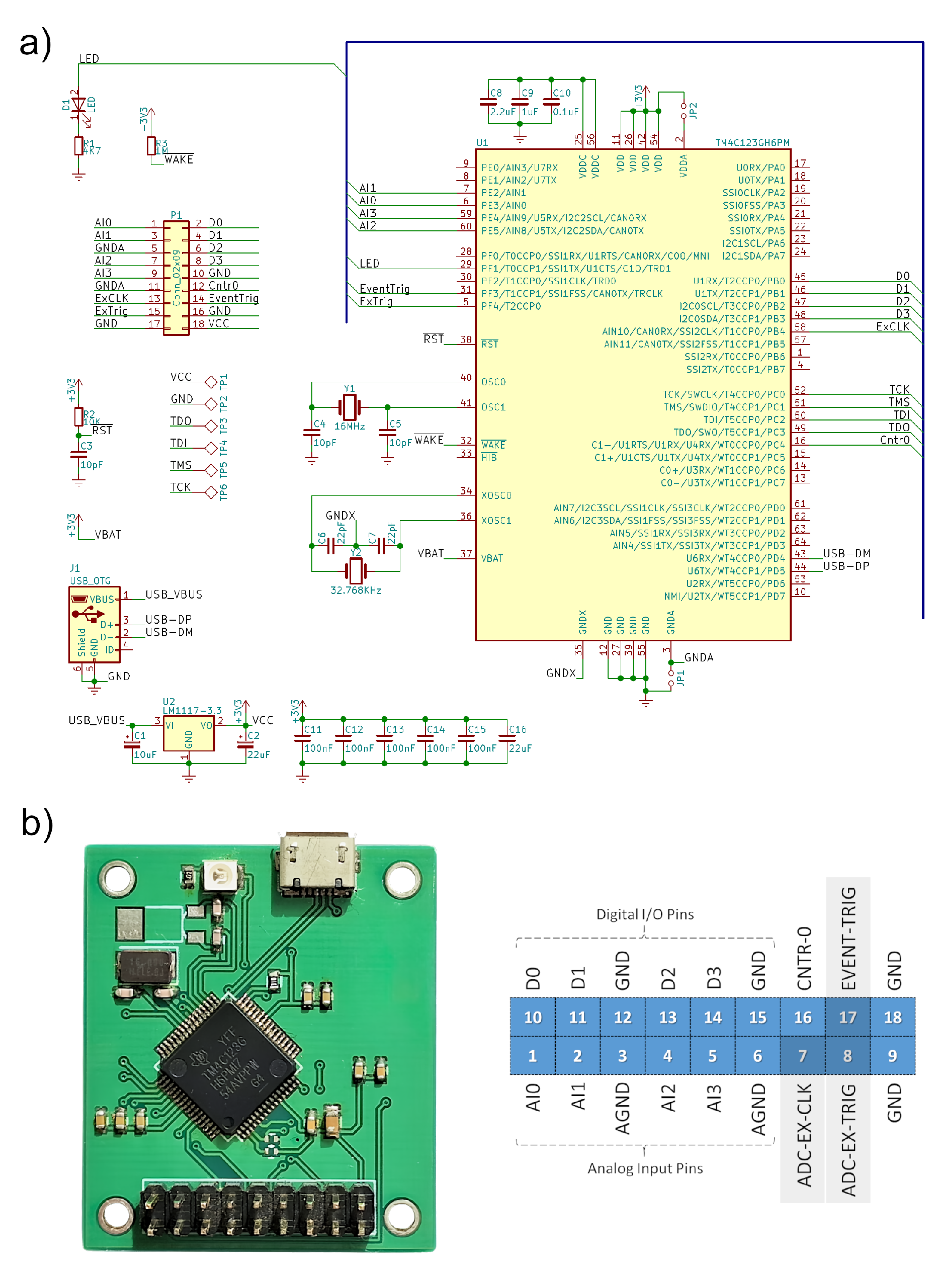
Figure 3.
The user interface is developed using Python and the PyQt5 library. The example signals visualize a 5 kHz sine (cyan) waveform and a 10 kHz square (magenta) waveform with a 25% duty cycle (sampled at 500 KSa/s). Both waveforms have an amplitude of 3.3 Vpp with a 1.65 V offset applied. The baseline of the square waveform is shifted to -4 V to visualize it in a separate region.
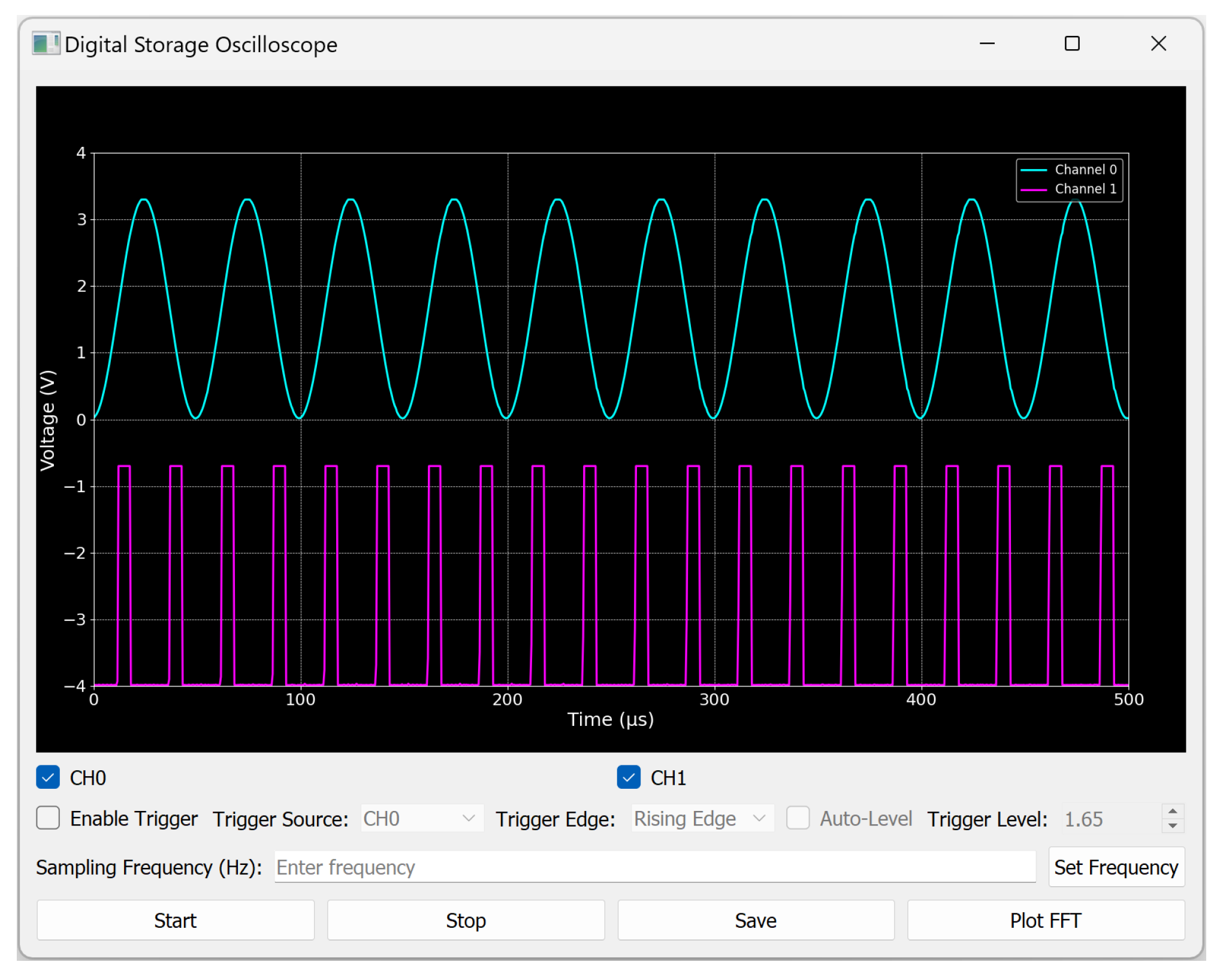
Figure 4.
The VI components in the developed LabVIEW package are used for configuring and operating the data acquisition system.
Figure 4.
The VI components in the developed LabVIEW package are used for configuring and operating the data acquisition system.
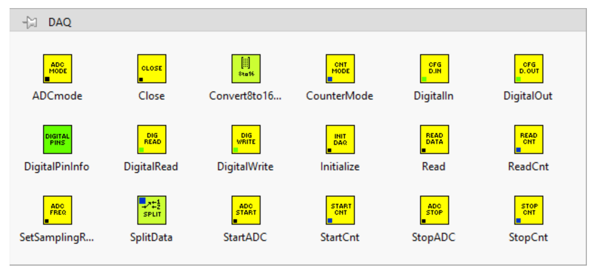
Figure 5.
The LabVIEW VI Front panel shows the example signals visualize a 5 kHz sine (cyan) waveform and a 10 kHz sawtooth (magenta) waveform (sampled at 500 KSa/s). Both waveforms have an amplitude of 3.3 Vpp with a 1.65 V offset applied. The baseline of the sawtooth waveform is shifted to -4 V to visualize it in a separate region.
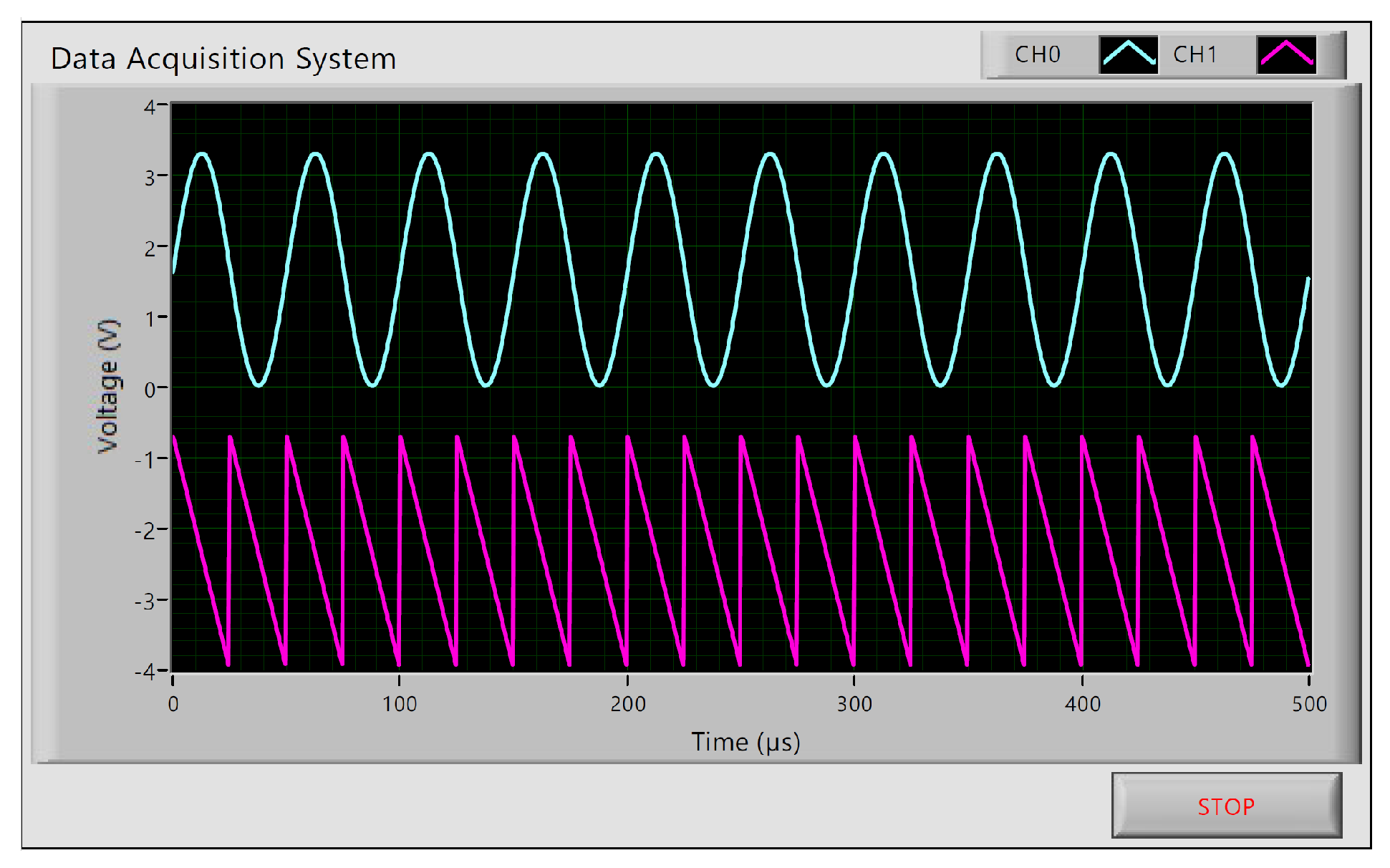
Figure 6.
Block diagram of the example VI. Here, the sampling rate is set to 500 KSa/s with 2 KSa samples, the trigger source is set to SW:Software, the ADC clock source to Onboard-clock, and the analog channels are AI0 and AI1 in a single-ended configuration.
Figure 6.
Block diagram of the example VI. Here, the sampling rate is set to 500 KSa/s with 2 KSa samples, the trigger source is set to SW:Software, the ADC clock source to Onboard-clock, and the analog channels are AI0 and AI1 in a single-ended configuration.
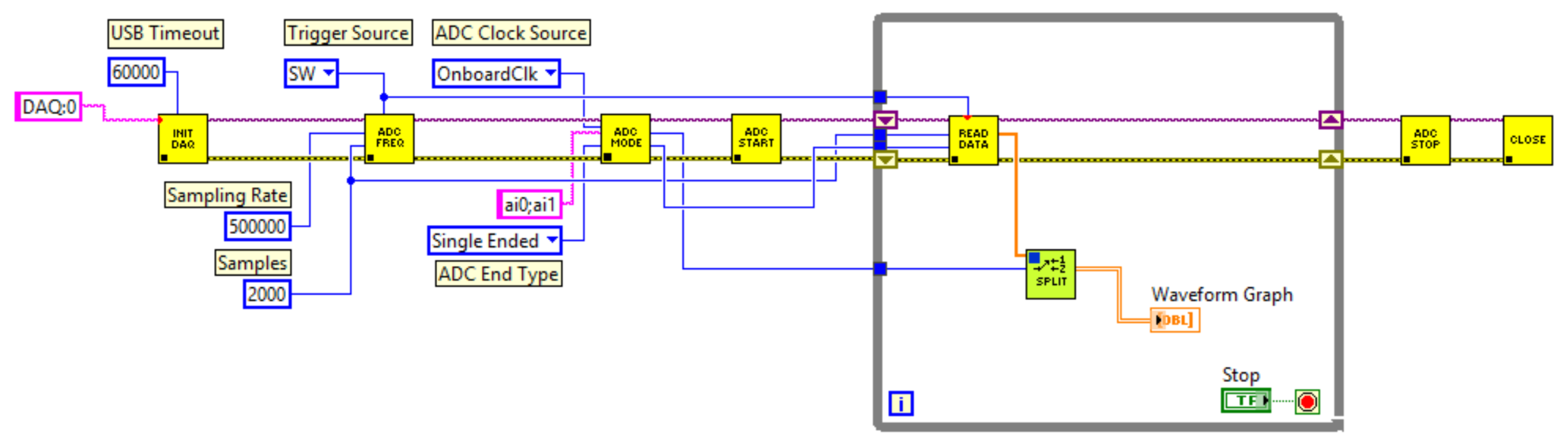
Figure 7.
A schematic representation of a coherent sampling setup for signal-to-noise and distortion measurement. To synchronize the ADC clock source with the AWG, a 1 MHz square wave is generated by the AWG to set the ADC sampling frequency to 1 MSa/s.
Figure 7.
A schematic representation of a coherent sampling setup for signal-to-noise and distortion measurement. To synchronize the ADC clock source with the AWG, a 1 MHz square wave is generated by the AWG to set the ADC sampling frequency to 1 MSa/s.
Disclaimer/Publisher’s Note: The statements, opinions and data contained in all publications are solely those of the individual author(s) and contributor(s) and not of MDPI and/or the editor(s). MDPI and/or the editor(s) disclaim responsibility for any injury to people or property resulting from any ideas, methods, instructions or products referred to in the content. |
© 2025 by the authors. Licensee MDPI, Basel, Switzerland. This article is an open access article distributed under the terms and conditions of the Creative Commons Attribution (CC BY) license (http://creativecommons.org/licenses/by/4.0/).
Copyright: This open access article is published under a Creative Commons CC BY 4.0 license, which permit the free download, distribution, and reuse, provided that the author and preprint are cited in any reuse.


