
Submitted:
13 March 2025
Posted:
13 March 2025
You are already at the latest version
Abstract
A one micron thick pure zinc oxide (ZnO) and nitrogen doped zinc oxide (N-ZnO) films, were fabricated on p-type, pristine (non-porous) and porous gallium nitride (GaN) substrates using a radio frequency (RF) sputtering technique at room temperature. The doping medium is nitrogen gas, which has a flow rate that ranges from 0 to 10 sccm (0 sccm refers to pure ZnO). Ultraviolet (UV) assisted photo electrochemical etching technique was employed to etch the wafer surface and develop porous GaN substrate. High-quality ZnO films were grown with ZnO powder as the target material under vacuum conditions. The X-ray diffraction (XRD) analysis confirms that the films grown on GaN possess a hexagonal wurtzite structure. For N-ZnO films, the UV-visible cut-off wavelength shifts towards the blue region. The root mean square (RMS) roughness of N-ZnO films, measured using atomic force microscopy (AFM), was found to decrease with increasing N-doping concentration. The lowest roughness value of 1.1 nm was observed for the 10 sccm sample, while the highest roughness of 3.4 nm was recorded for the pure ZnO film. The N-ZnO films was found to exhibit p-type conductivity as determined by Hall measurements using Van der Pauw method and the higher value of carrier concentration obtained for the nitrogen gas flow rate of 10 sccm, was 7.99 x 1018 cm-3.
Keywords:
zinc oxide films
; sputtering
; GaN template
; X-ray diffraction
; optical properties
1. Introduction
Zinc oxide (ZnO) thin films have attracted considerable attention due to their outstanding optical, electrical, and mechanical properties, making them highly suitable for diverse applications. ZnO is a wide-bandgap semiconductor (∼3.37 eV) with a high exciton binding energy (∼60 meV), ensuring strong excitonic emission even at room temperature. ZnO thin films exhibit excellent transparency in the visible region, high electrical conductivity when doped, and strong piezoelectric characteristics, making them ideal for optoelectronic devices, transparent conductive electrodes, sensors, and piezoelectric applications. These films can be deposited using various techniques, including sputtering, sol-gel processing, pulsed laser deposition, and chemical vapor deposition, each influencing their structural, morphological, and electrical properties. Besides, ZnO is extensively studied as a transparent conductive oxide thin film due to its high electron mobility, excellent transparency in the visible wavelength range, and low work function [1]. ZnO is an n-type material due to the existence of native defects such as zinc interstitial, oxygen vacancies, and other structural-related defects [2].
In general, ZnO-based optoelectronic devices are fabricated directly on Si substrates; however, achieving high internal quantum efficiency necessitates high-quality ZnO thin films. But, practically this is not possible due to their different crystal structures and thermal expansion coefficients [3]. The substrate plays a crucial role in film growth by controlling lattice and thermal mismatches between the substrate and the film, which contribute to stress formation in the deposited film. Moreover, the charge imbalance in the interface would cause many defects when ZnO thin films are growing because the abrupt interface is energetically unfavorable [4]. Therefore, the alternative findings are necessary and important to address this key issue on obtaining high-quality ZnO thin films. It is difficult to achieve high-quality epitaxial growth of ZnO, on glass substrate which is amorphous, resulting in polycrystalline films with grain boundaries and defects. The lack of epitaxial alignment and high defect density degrade the electrical properties of ZnO films [5]. ZnO films with a wurtzite structure are typically grown on (0001) Al2O3 substrates due to their structural similarity. However, there is a lattice mismatch of 30% between the basal planes of ZnO and Al2O3, along with an 18% mismatch between the smaller cell of Al atoms [6]. Özgür, Ü., et al. described the limitation of ZnO film grown on silicon substrate in which, ZnO and Si have a significant lattice mismatch (approximately 40%), which leads to the formation of defects such as dislocations and strain in the ZnO film [7]. The defects and strain in ZnO films grown on Si can lead to poor optical quality, including reduced photoluminescence efficiency and increased defect-related emission [8]. It was reported that ZnO deposited on Si, forms an amorphous interfacial layer of silicon oxide, (SiO2) at the ZnO/Si interface. This oxide layer can act as a barrier on transporting the charge carriers and reducing the electrical performance of devices [9]. Due to the chemical and structural differences between ZnO and Si, the adhesion of ZnO films to Si substrates can be poor, leading to delamination or peeling of the film [10]. Growing ZnO thin films on silicon substrates can negatively impact the film quality due to structural incompatibilities. ZnO has a wurtzite crystal structure, whereas Si possesses a diamond cubic structure, resulting in a lattice mismatch that can introduce strain and defects in the ZnO film. The thermal expansion coefficients between ZnO and Si can lead to thermal stress during the deposition of thin films [11,12] and this will deteriorate the optical property of the ZnO films. GaN substrate is considered for the growth of ZnO thin films, since the lattice mismatch between GaN and ZnO is relatively small [13]. Dong et al. discussed on producing cost-effective solid state lighting devices by combining zinc oxide (ZnO) and gallium nitride (GaN), by fabricating heterostructured LED device [14]. Both ZnO and GaN have a wurtzite crystal structure, which promotes epitaxial growth and reduces the formation of grain boundaries and defects [15] and this also enhance the photoluminescence efficiency and hinders defect-related emission. Thin films grown on porous substrates are found to be a greater relaxation of mismatch strain and have effectively reduced defect density through lateral dislocation bending mechanism [16]. GaN substrates have high thermal stability, allowing for high-temperature growth and processing of ZnO films without significant degradation in quality [17]. ZnO films grown on GaN substrates enhance the piezoelectric properties due to the high-quality epitaxial growth, making them suitable for piezoelectric devices and sensors [18].
Nitrogen (N) doping in ZnO has been extensively studied to modify its electrical and optical properties, particularly for achieving p-type conductivity in ZnO. Since intrinsic ZnO typically exhibits n-type conductivity due to native defects such as oxygen vacancies and zinc interstitials, the incorporation of nitrogen, a group-V element, aims to introduce acceptor states and compensate for the dominant donor defects. Nitrogen substitutes oxygen in the ZnO lattice, acting as an acceptor that can introduce hole carriers that facilitate hole conduction [19]. Nitrogen doping can shift photoluminescence (PL) emission peak of ZnO to the visible region, enhancing yellow-green emission due to the formation of nitrogen-related defect states. Nitrogen-doped ZnO exhibits improved photocatalytic performance, particularly under visible light irradiation. The introduction of nitrogen creates localized states within the bandgap, reducing the energy required for photoexcitation and enhancing the material's ability to drive photochemical reactions, such as water splitting for hydrogen production [20].
Reently, nitrogen doped ZnO thin films were fabricated on different substrates and by deposition techniques, to increase the optical transmittance and electrical conductivity for optoelectronic device applications [19,21]. Among various physical deposition techniques, magnetron sputtering is the most suitable for growing high-quality n-type doped ZnO thin films, as it allows precise control over the doping concentration while achieving a high deposition rate.
In this paper, ZnO films are grown on the non-porous and porous GaN substrates by employing the radio frequency (RF) magnetron sputtering technique at room temperature. The substrate purification and etching process was achieved on the surface of GaN substrate by using UV assisted photoelectrochemical etching technique for the production of porous GaN substrate. Later the pure and nitrogen doped ZnO films was subsequently grown on the etched porous GaN substrate. The effect of substrates and nitrogen doping on morphological, structural, electrical and optical properties of the grown ZnO films were analysed and the obtained results were discussed in detail.
2. Experimental Techniques
2.1. Preparation of Porous GaN Substrate
In this experiments, porous GaN template was utilized as one of the substrates along with non-porous (pristine) substrate for the growth of ZnO and N-doped films. The commercial unintentionally doped n-type 2-inch diameter of GaN wafer (from Technologies and Devices International Inc., USA) was used in this experiment as a substrate for the growth of ZnO film. The thickness of GaN film was about 3.0 μm with carrier concentration of about ~4.38×1017 cm−3. The total process was executed in two different stages. In the first stage, a porous gallium nitride template was achieved by UV-assisted photo electrochemical etching in a custom-made Teflon cell containing a mixture of sulphuric acid (H2SO4) and hydrogen peroxide (H2O2) with a 3:1 volume ratio. Platinum wire and GaN substrates acted as the cathode and the anode, respectively. The porous gallium nitride was formed at a constant current density of 10 mA/cm2, under the illumination of a UV lamp with 500W power for an etching period of 60 minutes to develop sufficient deep porous nanostructures. The etched template was thoroughly rinsed with deionized (DI) water and then dried with high-purity nitrogen gas prior to the coating process [22].
2.2. Preparation of Pure and N-Doped ZnO Films on GaN Substrate
In the second stage of the experiment, HHV A500 radio frequency (RF) sputtering system was employed with zinc oxide (ZnO) target (99.999% purity) to deposit ZnO films on GaN substrate. The base pressure was 3×10⁻⁵ mbar, which was raised to 2×10⁻² mbar by purging the chamber with high purity argon that served as the sputtering gas and the maintained power of the sputtering was 150 W. For N-ZnO films, the nitrogen gas flow rate was varied between 0-10 sccm in steps of 2 sccm (sccm denotes cubic centimeter per minute) through a mass flow controller. One micron-thick ZnO films were deposited onto both nonporous and porous gallium nitride (GaN) substrates. The grown pure and N-doped ZnO films on both the substrates were then annealed in a tube furnace at 500 °C under a nitrogen atmosphere for one hour. The growth parameters are presented in Table 1.
2.3. Characterisation Techniques
The surface topographical features of pristine and porous gallium nitride and the deposited ZnO films were visualized by employing field emission scanning electron microscopy (FESEM) (model FEI/NovaNanoSEM450). The morphology and roughness of the grown films were investigated through atomic force microscope (AFM, Model: Dimension Edge, Bruker). The crystalline structure and the film growth orientation were ascribed with X-ray diffraction (XRD) (PAN analytical X’Pert PROMRDPW3040) with CuKα radiation wavelength of 0.154 nm. The optical properties of the GaN substrate and the deposited ZnO films were analysed at room temperature with JobinYvon HR 800UV, Edison, NJ, USA equipment. He–Cd laser (325 nm) and an argon ion laser (514.5 nm) were used as excitation sources for photoluminescence (PL) and Raman measurements, respectively. The electrical properties of the pure and nitrogen-doped ZnO films, including electrical resistivity, carrier concentration, and electron mobility, were measured using a Hall Effect system (Model: Lakeshore Controller 601/DRC-93CA).
3. Results and Discussion
3.1. Structural and Optical Analysis of GaN Substrates
3.1.1. SEM Analysis of Pristine and Porous GaN Substrate
Photoelectrochemical etching process was adapted for modifying the surface of GaN substrate. Porous nanostructure was developed on the flat GaN substrate surface (shown in Figure 1(a)) due to the energy band bends downward by the application of the bias that depletes electrons from the substrate material [23]. In this course of action, holes were accumulated that oxidizes the substrate surface by the injection of electrons. While the etchant subsequently dissolves the produced oxides, the substrate surface was turned into porous structure that was further enhanced by incorporating the illumination of UV light during the etching reaction was shown are shown in Figure 1 (b) and (c) with an enlarged image. The SEM image of the porous GaN surface exhibit that the developed pores are spherical in shape [24].
3.1.2. Raman Spectral Analysis of Pristine and Porous GaN Substrate
Raman spectral analysis was conducted at room temperature to investigate the phonon modes present, as illustrated in Figure 2. As can be seen that, two such modes E2 (TO) and A1 (LO) are observed in the Raman spectra for the non-porous and porous gallium nitride substrates [25]. The obtained Raman peaks are located at 532 cm−1 for A1 (TO) phonon, 568.2 cm−1 for E2 (high) phonon, and at 740 cm−1 for A1 (LO) phonon modes, respectively. Here, we observed the A₁ (LO) phonon peak at 750.2 cm−1 for the etched porous GaN. Due to the efficient coupling of Raman scattered radiation, the surface nanostructure enhances the substrate quality of porous GaN and delivers higher Raman intensity compared to an unetched GaN substrate. Moreover, all these modes exhibit a red shift to higher frequencies compared to the unetched pristine GaN substrate. This shift is attributed to the relaxation of compressive stress in the etched substrate, driven by the quantum confinement effect of the porous structures [26]. However, the observed Raman shift is slightly lower, indicating minimal stress from defects. This confirms that the etched porous GaN wafer in this study is nearly stress-free and suitable for ZnO film deposition [27]. The improvement of the substrate quality might be attributed to the disordering crystalline structure.
3.2. Structural, Morphological and Electrical Properties ZnO Films
3.2.1. XRD Analysis of Pure and Nitrogen Doped ZnO on Porous GaN Substrate
To evaluate the crystalline nature of the grown ZnO films, high-resolution X-ray diffraction (HRXRD) analysis was performed, and the resulting diffraction curves are presented in Figure 3(a)–(c). Figure 3(a) and (b) illustrates the pure zinc oxide film grown on non-porous and porous GaN substrate, respectively. These diffraction peaks indicate that the deposited films has hexagonal wurtzite phase, verified with standard data card No. 00-005-0664 [28]. The compiled XRD data for the nitrogen doped ZnO (N-ZnO) films deposited on porous GaN subtrate is shown in Figure 3(c). It is confirmed that the high-quality ZnO films were grown on porous GaN substrate than non-porous substrate by having a narrow and high intense diffraction peak of ZnO with the same crystal orientation of GaN. It was observed that the grown epitaxial film on both substrates was oriented along (002) crystal plane at 2θ = 34°. It was detected that all the ZnO films were grown with a preferred orientation along the c-axis. As shown in Figure 3(b), the epitaxial ZnO film grown on a porous substrate exhibits an additional low-intensity peak at 36.36°, corresponding to the ZnO (101) plane. The diffraction peaks associated with porous GaN substrate also has very high diffraction intensities towards the same crystal orientation of ZnO. The presence of high intense diffraction peaks ensures excellent crystal quality of ZnO films on porous GaN is due to the stress-free and reduced defects compared to a film grown on non-porous substrate. Nitrogen doping could also reduce the crystallite size, and accompanied by peak broadening in the XRD pattern [29].
It is well known that doping ions are more likely to occupy substitutional sites rather than interstitial sites due to the lower energy barrier associated with nitrogen incorporation [30]. The diffraction data did not reveal any additional nitrogen-related diffraction peaks, indicating that nitrogen is incorporated solely into the ZnO lattice. This confirms the absence of any secondary nitrogen compounds or complexes [31]. The ionic radius of O²⁻ is 1.40 Å (140 pm), which is slightly smaller than that of N³⁻ (1.46 Å). This smaller difference in ionic radii can lead to lattice distortion or strain when nitrogen is doped into ZnO and expected that N atoms would preferably substituting O atoms in the crystal lattice of ZnO. When N3- replaces O2- in the ZnO lattice during doping, it acts as an acceptor, compensating for oxygen vacancies and reducing both defect density and the concentration of conduction electrons. The low intense (101) peak of the grown films were carefully examined by magnifing the peak for pure and N-ZnO samples as shown in Figure 3(d), to confirm the substitution of nitrogen in the ZnO lattice. It was clear that (101) peak get shifted towards higher angle with reasonable peak broadening compared with pure ZnO film. The peak shift observed in all N-doped films compared to undoped ZnO indicates interstitial nitrogen doping, leading to lattice contraction due to internal strain [32,33,34]. Increased peak broadening suggests smaller crystallite size or lattice defects caused by nitrogen incorporation affecting electronic and optical properties of ZnO films.
3.2.2. SEM Analysis of Pure and Nitrogen Doped ZnO on Porous GaN Substrate
The SEM micrographs of the grown pure ZnO films on both non-porous and porus substrates were shown in Figure 4(a) and (b) respectively. Additionally, the nitrogen doped ZnO film deposited on porous GaN substrate is presented in Figure 4(c). From the images it was evidenced that all the grown pure and nitrogen doped ZnO films were well adhered to the substrate using sputtering technique. Comparing to the ZnO film on non-porous substrate, the film which was deposited on the porous substrate have labyrinth patterns due to the release of air during the annealing process to produce a kind of growth pattern presenting several nanoparticles of ZnO clumping together to form agglomerated structure [35]. It is attributed that the pores in the GaN substrate were filled with ZnO particles and having matrix with GaN which effectively modifies the substrate nature by releasing the stress present in the substrate. This predominately improves the film quality by minimizing the dislocations of the grown films, compared to non-porous substrate films.
3.2.3. Atomic Force Microscopic Analysis of Pure ZnO and N-ZnO Films
Figure 6 shows the AFM topographical images of the pure ZnO and nitrogen-doped ZnO (N-ZnO) film deposited on gallium nitride (GaN) substrates. The AFM images were scanned over a 5 µm × 5 µm area of the sample, as shown in Figure 5(a) and (b), respectively for the pure ZnO film deposited on non-porous and porous GaN substrate. Figure 5(c-g) represents the N-ZnO film deposited on porous GaN substrate, respectively. AFM images shown the grown metal oxide films on porous GaN have a smooth and compact morphology which is highly favors solar cell device performance [36]. The surface was composed of high dense homogenous grains for each film sample and we observed the grain size decreases gradually towards the higher nitrogen content in ZnO film. As seen in 3D AFM images of the surface, grain growth found to be dense with highly homogenous distribution with smaller RMS values on doping [37]. The root means square (RMS) values of the ZnO films on non-porous and porous GaN substrtaes were tabulated in the Table 2. It was clear that the RMS (roughness) value obtained from AFM images for the films deposited on porous GaN decreases, compared to films grown on an unetched (non-porous) substrate. The obtained RMS value for the pure ZnO film grown on a non-porous GaN was 11.2 nm, while the same was decreased to 3.4 nm when the film was grown on a porous GaN substrate. This confirms that the porous structure of GaN favors smoothing the ZnO film surface during the particles deposition over the substrate. This smoothing behavior significantly enhances the diffusion ability of the atoms, resulting in a notable reduction in surface roughness. Consequently, the film quality is improved compared to the ZnO film grown on a non-porous substrate. For the N-ZnO film sample with a gas flow rate of 10 sccm, a low roughness value of 1.1 nm was observed on the porous GaN substrate.
3.2.4. Photoluminescence Analysis of ZnO Films on GaN Substrates
The photoluminescence spectra of the ZnO films grown on both pristine and porous GaN substrates were shown in Figure 6. Two emission peaks are observed in both films, namely near band edge (NBE) emission and the deep level (DLE) emission in visible region, respectively. NBE emission peak at 375 nm and low intense broader DLE emission peak is observed for both samples. However, the obtained peak for the film grown on the porous substrate having significantly narrower with increasing intensity compared to the film grown on the non-porous GaN substrate. It is attributed that the substantial enhancement of the luminescence efficiency by suppressing the inherently associated substrate-induced stress and the growth-associated dislocations in ZnO films on GaN, which illustrates that the high optical quality film was grown on the porous GaN substrate. Moreover, higher surface to volume ratio of the porous structure enormously increase the electrons concentration for participating in the photoluminescence process, as a result emitted photons is higher in porous GaN and the porosity has the dominant influence on the enhancement of emission intensity. Further it is noted that the low intense broader DLE peak shifted towards red region for the ZnO film on porous GaN, from the green region of ZnO film on grown non-porous GaN substrate.
3.2.5. UV-Visible Specrtra of ZnO Films on GaN Template
The optical properties of the undoped and nitrogen doped ZnO films on GaN template were recorded by the UV-visble optical transmittance spectra in the wavelength region 300 to 2000 nm is displayed in Figure 7. The obtained transmission spectra consist the interference oscillations because of the film thickness and difference in the refraction of incident light between the film and the substrate. In the nitrogen-doped ZnO films, cut-off wavelength is blue-shifted by 8 nm (i.e. from 374 nm to 367 nm) for different gas flow rate. It is also considered that the widening of the band gap of ZnO film is due to the effect of nitrogen doping in the lattice. It was attributed that ZnO film doping with nitrogen atom shifted the Fermi level below the valence band by the excess of the hole concentration that widen the band gap of the grown films [38]. The magnified UV-Vis transmittance spectra in the inset of Figure 7 clearly show a blue shift in the N-ZnO film samples with increasing nitrogen doping content, supporting our previous findings [22].
3.2.6. Electrical Properties of ZnO Films on GaN Substrate
The Hall measurements was executed to investigate the electrical properties, including carrier mobility, carrier concentration and electrical resistivity for pure ZnO film and nitrogen doped ZnO films (N-ZnO) by adapting van der Pauw technique [39,40] and the obtained results were plotted in Figure 8. From the plot we found that all the pure ZnO and N-doped ZnO films were exhibited p-type conductivity due to the acceptor level incorporation in the ZnO lattice by the inclusion of dopant nitrogen [41]. The nitrogen doped ZnO sample with 6 sccm nitrogen gas flow rate found to have slightly higher resistivity than other doped samples. This decrement in conductivity at higher doping level, causing nitrogen to form complexes such as N2 molecules or creating N-O defects, which reduces conductivity or lead to semi-insulating behavior in ZnO film [42]. The electrical resistivity was found to be decreased drastically in several orders of magnitude such as 10−3 Ω-cm, while the undoped sample has resistivity 1.095 Ω-cm. This resistivity decrement in the doped films greatly improved the hole concentration from 1017 to 1021 cm-3. The obtained hole concentration values measured from Hall measurements for the deposited films are 2.12 x 10¹⁸, 8.54 x 10¹⁹, 4.40 x 10²¹, 5.29 x 10²¹, and 7.99 x 1018 cm−3 for 2 sccm, 4 sccm, 6 sccm, 8 sccm, and 10 sccm, respectively. The N-ZnO sample with 8 sccm nitrogen gas flow rate found to have higher carrier concentration 5.29 x 1021 cm−3. The decreased hole concentration at higher nitrogen doping was due to the pinning of the Fermi level [43]. The mobility of the nitrogen-doped films exhibits a zigzag pattern. The increase in the nitrogen flow rate effectively decrease the mobility by intensifying the ionized impurity scattering in the ZnO lattice. This might be the sample having lower hole concentration reduces the grain boundary scattering compared with all other doped samples. The N-ZnO film with 4 sccm nitrogen gas flow rate delivers high mobility than other film samples. In contrast for the sample with nitrogen flow rate of 10 sccm, the carrier mobility is found to be increasing again. The decrease in mobility with increase in nitrogen doping, consistent with increased scattering from defects and impurities which caused by nitrogen doping inducing defects created by the presence of N2, or N-O complexes, which act as scattering centers [44].
4. Conclusions
A porous structure was developed on the surface of gallium nitride (GaN) substrates, and pure zinc oxide (ZnO) nanoparticles were deposited onto it. For comparison, N-ZnO films were also grown on non-porous GaN substrates to study the influence of the substrate on the quality of the as-grown ZnO films. Ultra violet light assisted photoelectrochemical etching technique was adapted to develop the porous nanostructure over the surface of pristine GaN substrate. Physical evaporation coating technique and radio frequency magnetron sputtering method were used to deposit the metal oxide films over both porous and non-porous GaN substrates at room temperature. The obtained FESEM micrographs of GaN surface revealed the development of spherical shape pores having an excellent porous network throughout the surface of the substrate without any ridge morphology. The deposited ZnO thin film was well adhered with the porous GaN substrate due to filling of ZnO nanoparticles in the pores and production of labyrinth patterns compared to the deposition of particles on non-porous substrate. The XRD pattern revealed that the grown ZnO film over porous substrate establish better diffraction intensity towards (002) crystalline orientation. In the UV-Vis transmittance spectra, the increasing nitrogen doping level in the ZnO films caused the cut-off wavelength shifted towards blue region by 8 nm, i.e. from 374 to 367 nm, which could be ascribed to widening of band gap. The emission properties of the N-doped films got sufficiently improved through the nanostructuring process which was further ascertained with the enhancement of luminescence intensity. Besides, the allowed phonon modes get red-shifted in the Raman spectral data determines the relaxation of the compressive stress present in the porous GaN substrate. Hall measurements confirmed that all the nitrogen doped ZnO films demonstrated p-type property with better electrical conductivity. The nitrogen-doped ZnO film with an 8 sccm nitrogen gas flow rate was found to exhibit a higher carrier concentration.
Author Contributions
Investigation and Methodology, R. Perumal; Manuscript draft, Lakshmanan Saravanan; Supervision, Jih-Hsin Liu.
Funding
This research was funded by Tunghai University and the National Science and Technology Council, Taiwan, R.O.C., grant number NSTC 112-2622-E-029-007.
Conflicts of Interest
The author declare that they have no conflict of interest.
References
- Tian, Z.R.; Voigt, J.A.; Liu, J.; Mckenzie, B.; Mcdermott, M.J.; Rodriguez, M.A.; Xu, H. Complex and oriented ZnO nanostructures. Nat. Mater. 2003, 2, 821–826. [Google Scholar] [CrossRef]
- Seghier, D.; Gislason, H.P. Shallow and deep donors in n-type ZnO characterized by admittance spectroscopy. J. Mater. Sci.: Mater. Electron. 2008, 19, 687–691. [Google Scholar] [CrossRef]
- Klingshirn, C. ZnO: Material, physics, and applications. ChemPhysChem. 2007, 8, 782–803. [Google Scholar] [CrossRef] [PubMed]
- Wang, L.; Liu, Y.C.; Xu, C.S.; Qiu, Y.Q.; Zhao, L.; Rong, X.M. Effect of nitrogenized Si (111) substrates on the quality of ZnO films grown by pulsed laser deposition. J. Phys. D: Appl. Phys. 2009, 42, 035307. [Google Scholar] [CrossRef]
- Fortunato, E.; Barquinha, P.M.C.; Pimentel, A.C.M.B.G.; Gonçalves, A.M.F.; Marques, A.J.S.; Martins, R.F.P.; Pereira, L.M.N. Wide-bandgap high-mobility ZnO thin-film transistors produced at room temperature. Appl. Phys. Lett. 2004, 85, 2541–2543. [Google Scholar] [CrossRef]
- Chen, Y.; Ko, H.J.; Hong, S.K.; Yao, T. Layer-by-layer growth of ZnO epilayer on Al2O3(0001) by using a MgO buffer layer. Appl. Phys. Lett. 2000, 76, 559. [Google Scholar] [CrossRef]
- Özgür, Ü.; Alivov, Ya. I.; Liu, C.; Teke, A.; Reshchikov, M.A.; Doğan, S.; Avrutin, V.; Cho, S.-J.; Morkoç, H. A comprehensive review of ZnO materials and devices. J. Appl. Phys. 2005, 98, 041301. [Google Scholar] [CrossRef]
- Vanheusden, K.; Warren, W.L.; Seager, C.H.; Tallant, D.R.; Voigt, J.A.; Gnade, B.E. Mechanisms behind green photoluminescence in ZnO phosphor powders. J. Appl. Phys. 1996, 79, 7983–7990. [Google Scholar] [CrossRef]
- Pearton, S.J.; Norton, D.P.; Ip, K.; Heo, Y.W.; Steiner, T. Recent progress in processing and properties of ZnO. Superlattices Microstruct. 2003, 34, 3–32. [Google Scholar] [CrossRef]
- Wang, Z.L. Zinc oxide nanostructures: Growth, properties, and applications. J. Phys.: Condens. Matter. 2004, 16, R829–R858. [Google Scholar] [CrossRef]
- Hanada, T. Basic Properties of ZnO, GaN, and Related Materials. In Oxide and Nitride Semiconductors. Advances in Materials Research, Yao, T.; Hong, S.K. Ed.; Springer, Berlin, Heidelberg, 2009, Volume 12.
- Chao, C.H.; Wei, D.H. Synthesis and characterization of high c-axis ZnO thin film by plasma enhanced chemical vapor deposition system and its UV photodetector application. J. Vis. Exp. 2015, 3, 53097. [Google Scholar] [CrossRef]
- Hamdani, F. ; Yeadon, M.; Smith, D. J.; Tang, H.; Kim, W.; Salvador, A.; Botchkarev, A. E.; Gibsor, J. M.; Polyakov, A. Y.; Skowronski, M.; Morkoc, H. J. Appl. Phys. 1998, 83, 983.
- Dong, J.J.; Zhang, X.W.; Yin, Z.G.; Wang, J.X.; Zhang, S.G.; Liu, X. Ultraviolet electroluminescence from ordered ZnO nanorod array/p-GaN light emitting diodes. Appl. Phys. Lett. 2012, 100, 171109. [Google Scholar] [CrossRef]
- Look, D.C. Recent advances in ZnO materials and devices. Mater. Sci. Eng. B, 2001, 80, 383–387. [Google Scholar] [CrossRef]
- Inoki, C.K.; Kuan, T.S.; Lee, C.D.; Sagar, A.; Feenstra, R.M.; Koleske, D.D.; Adesida, I. Growth of GaN on porous SiC and GaN substrates. J. Electron. Mater. 2003, 32, 855–860. [Google Scholar] [CrossRef]
- Norton, D.P.; Heo, Y.W.; Ivill, M.P.; Ip, K.; Pearton, S.J.; Chisholm, M.F.; Steiner, T. ZnO: Growth, doping, and processing. Mater. Today, 2004, 7, 34–40. [Google Scholar] [CrossRef]
- Wang, Z.L. Nanopiezotronics. Adv. Mater. 2007, 19, 889–892. [Google Scholar] [CrossRef]
- Shafiqul, I.M.; Deep, R.; Lin, J.; Yoshida, T.; Fujita, Y. The Role of nitrogen dopants in ZnO nanoparticle-based light emitting diodes. Nanomaterials. 2022, 12, 358. [Google Scholar] [CrossRef]
- Cerrato, E.; Privitera, A.; Chiesa, M.; Salvadori, E.; Paganini, M.C. Nitrogen-doped Zinc oxide for photo-driven molecular hydrogen production. Int. J. Mol. Sci. 2022, 23, 5222. [Google Scholar] [CrossRef]
- Musiliyu, K.A.; Ogunmola, E.D.; Ajayi, A.A.; Abodunrin, O.W. Effect of concentration on the properties of nitrogen-doped zinc oxide thin films grown by electrodeposition. Mater. Renew. Sustain. Energy. 2023, 12, 23–29. [Google Scholar] [CrossRef]
- Perumal, R.; Hassan, Z. Effect of nitrogen doping on structural, morphological, optical and electrical properties of radio frequency magnetron sputtered zinc oxide thin films. Physica B Condens. Matter. 2016, 490, 16–20. [Google Scholar] [CrossRef]
- Seo, J.W.; Oh, C.S.; Cheong, H.S.; Yang, J.W.; Youn, C.J.; Lim, K.Y. UV-assisted electrochemical oxidation of GaN. J. Korean Phys. Soc. 2002, 41, 1017–1020. [Google Scholar]
- Yam, F.K.; Hassan, Z.; Ng, S.S. Porous GaN prepared by UV assisted electrochemical etching. Thin solid films, 2007, 515, 3469–3474. [Google Scholar] [CrossRef]
- Davydov, V.Y.; Kitaev, Y.E.; Goncharuk, I.; Smirnov, A.; Graul, J.; Semchinova, O.; Uffmann, D.; Smirnov, M.; Mirgorodsky, A.; Evarestov, R. Phonon dispersion and Raman scattering in hexagonal GaN and AlN. Phys. Rev. B. 1998, 58, 12899. [Google Scholar] [CrossRef]
- Al-Heuseen, K.; Hashim, M.R.; Ali, N.K. Effect of different electrolytes on porous GaN using photo-electrochemical etching. Appl. Surf. Sci. 2011, 257, 6197–6201. [Google Scholar] [CrossRef]
- Zeng, Y.; Ning, J.; Zhang, J.; Jia, Y.; Yan, C.; Wang, B.; Wang, D. Raman analysis of E2 (High) and A1 (LO) phonon to the stress-free GaN grown on sputtered AlN/Graphene buffer layer. Appl. Sci. 2020, 10, 8814. [Google Scholar] [CrossRef]
- Abed, C.; Bouzidi, C.; Elhouichet, H.; Gelloz, B.; Ferid, M. Mg doping induced high structural quality of sol–gel ZnO nanocrystals: Application in photocatalysis. Appl. Surf. Sci. 2015, 349, 855–863. [Google Scholar] [CrossRef]
- Ibrahim, K.M.; Saleh, W.R.; Al-Sammarraie, A.M.A. Structural and optical properties of ZnO nanostructures synthesized by hydrothermal method at different conditions. Nano Hybrids and Composites, 2022, 35, 75–83. [Google Scholar] [CrossRef]
- Ahmed, F.; Kumar, S.; Arshi, N.; Anwar, M.S.; Koo, B.H. Morphological evolution between nanorods to nanosheets and room temperature ferromagnetism of Fe-doped ZnO nanostructures. Cryst. Eng. Comm. 2012, 14, 4016–4026. [Google Scholar] [CrossRef]
- Tu, M.-L.; Su, Y.-K.; Ma, C.-Y. Nitrogen-doped p-type ZnO films prepared from nitrogen gas radio-frequency magnetron sputtering. J. Appl. Phys. 2006, 100, 053705–053708. [Google Scholar] [CrossRef]
- Zhang, X.; Qin, J.; Xue, Y.; Yu, P.; Zhang, B.; Wang, L.; Liu, R. Effect of aspect ratio and surface defects on the photocatalytic activity of ZnO nanorods. Sci. Rep. 2014, 4, 4596. [Google Scholar] [CrossRef] [PubMed]
- Siva, N.; Sakthi, D.; Ragupathy, S.; Arun, V.; Kannadasan, N. Synthesis, structural, optical and photocatalytic behavior of Sn doped ZnO nanoparticles. Mater. Sci. Eng. B. 2020, 253, 114497. [Google Scholar] [CrossRef]
- Hirai, M.; Kumar, A. Infrared Lattice Vibrations of Nitrogen-doped ZnO Thin Films. Mater. Res. Soc. Symp. Proc. 2007, 1035, 707. [Google Scholar] [CrossRef]
- Decremps, F.; Datchi, F.; Saitta, A.M.; Polian, A.; Pascarelli, S.; Di Cicco, A.; Baudelet, F. Local structure of condensed zinc oxide. Phys. Rev. B. 2003, 68, 104101. [Google Scholar] [CrossRef]
- Kang, J.H.; Song, A.; Park, Y.J.; Seo, J.H.; Walker, B.; Chung, K.-B. Tungsten-doped zinc oxide and indium–zinc oxide films as high-performance electron-transport layers in N–I–P perovskite solar cells. Polymers, 2020, 12, 737. [Google Scholar] [CrossRef]
- Dimitrov, D.; Tsai, C.-L.; Petrov, S.; Marinova, V.; Petrova, D.; Napoleonov, B.; Blagoev, B.; Strijkova, V.; Hsu, K.Y.; Lin, S.H. Atomic layer-deposited Al-doped ZnO thin films for display applications. Coatings 2020, 10, 539. [Google Scholar] [CrossRef]
- King, P.D.C.; Veal, T.D.; Fuchs, F.; Wang, C.Y.; Payne, D.J.; Bourlange, A.; Zhang, H.; Bell, G.R.; Cimalla, V.; Ambacher, O.; Egdell, R.G.; Bechstedt, F.; McConville, C.F. Band gap, electronic structure, and surface electron accumulation of cubic and rhombohedral In2O3. Phys. Rev. B. 2009, 79, 205211–10. [Google Scholar] [CrossRef]
- van der Pauw, L.J. A method of measuring specific resistivity and Hall effect of discs of arbitrary shape. Philips Res. Rep. 1958, 13, 1–9. [Google Scholar]
- Imasato, K.; Kang, S.D.; Ohno, S.; Snyder, G.J. Band engineering in Mg3Sb2 by alloying with Mg3Bi2 for enhanced thermoelectric performance. Mater. Horiz. 2018, 5, 59–64. [Google Scholar] [CrossRef]
- Keavney, D.J.; Buchholz, D.B.; Ma, Q.; Chang, R.P.H. Where does the spin reside in ferromagnetic Cu-doped ZnO? Appl. Phys. Lett. 2007, 91, 012501. [Google Scholar] [CrossRef]
- Erhart, P.; Albe, K.; Klein, A. First-principles study of intrinsic point defects in ZnO: Role of band structure, volume relaxation, and finite-size effects. Phys. Rev. B. 2006, 73, 205203. [Google Scholar] [CrossRef]
- Zhang, S.B.; Wei, S.H.; Zunger, A. Microscopic Origin of the Phenomenological Equilibrium “Doping Limit Rule” in n-Type III-V Semiconductors. Phys. Rev. Lett. 2000, 84, 1232–1235. [Google Scholar] [CrossRef] [PubMed]
- Wang, L.Y.; Mal'shukov, A.G.; Chu, C.S. Nonuniversality of the intrinsic inverse spin-Hall effect in diffusive systems. Phys. Rev. B. 2012, 85, 165201. [Google Scholar] [CrossRef]
Figure 1.
FESEM images of GaN substrates (a) non-etched GaN (b) porous GaN and (c) magnified image of porous GaN.
Figure 1.
FESEM images of GaN substrates (a) non-etched GaN (b) porous GaN and (c) magnified image of porous GaN.
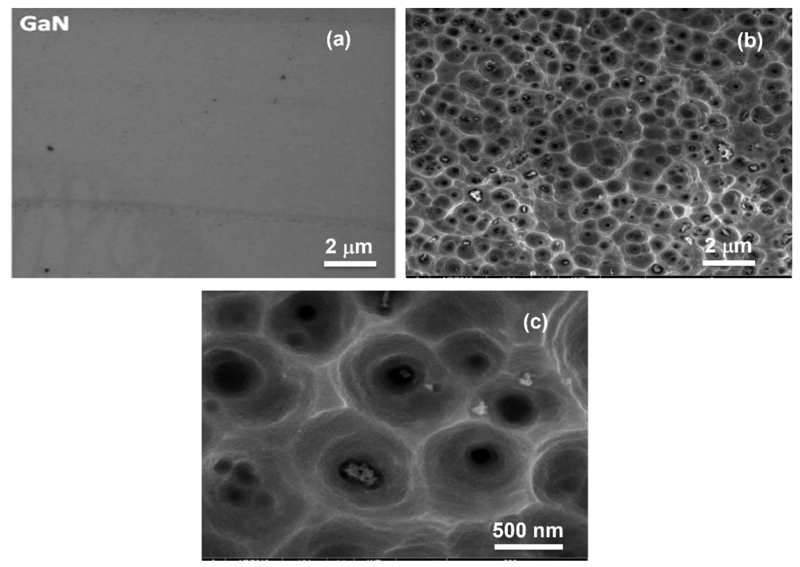
Figure 2.
Raman spectra of non-porous (GaN) and porous GaN (PGaN) substrates.
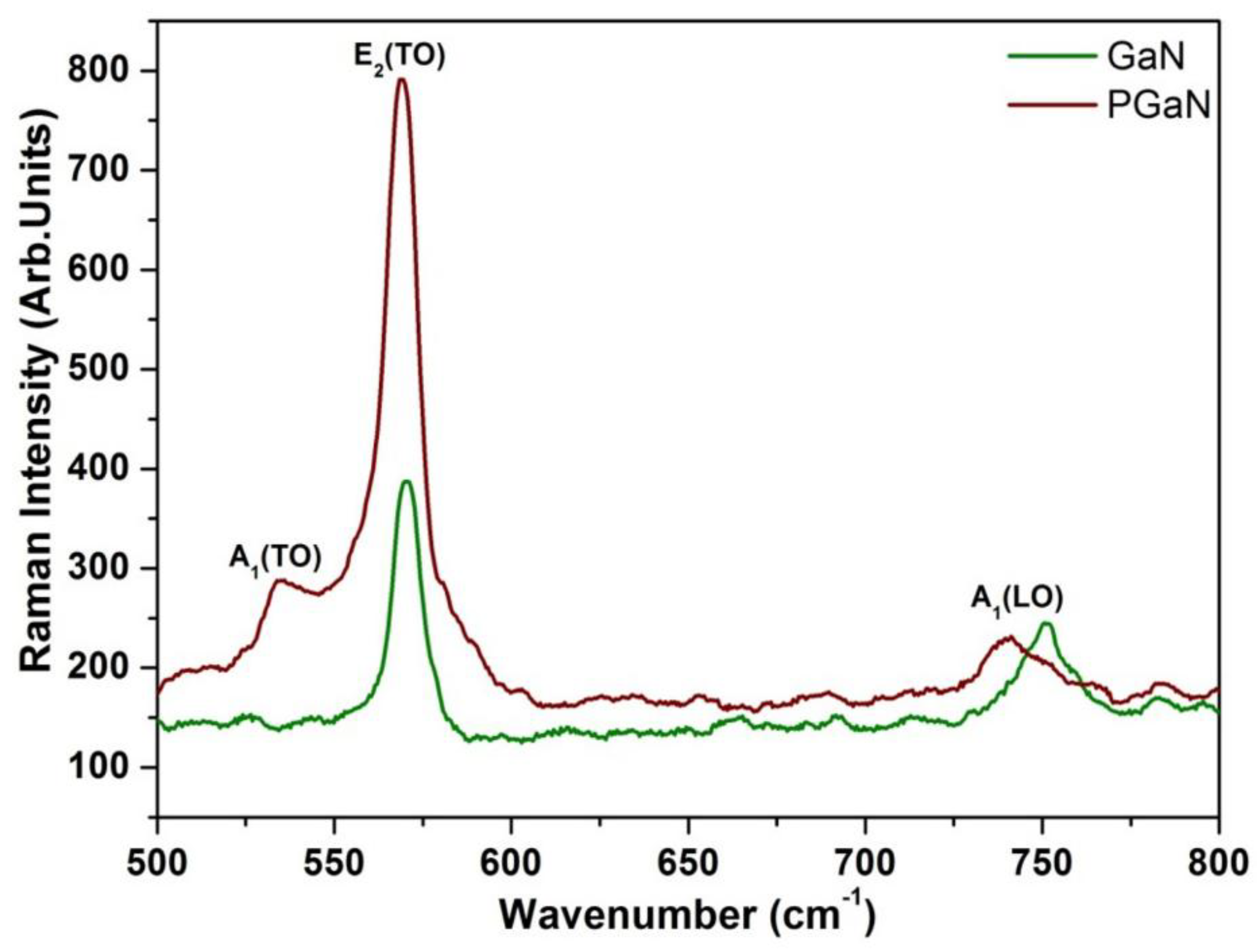
Figure 3.
Thin film XRD pattern of (a) pure ZnO film deposited on pristine non-etched GaN and (b) pure ZnO film deposited on porous GaN substrate. XRD for (c) nitrogen doped ZnO films and (d) magnified (101) ZnO peaks for nitrogen doped ZnO film samples.
Figure 3.
Thin film XRD pattern of (a) pure ZnO film deposited on pristine non-etched GaN and (b) pure ZnO film deposited on porous GaN substrate. XRD for (c) nitrogen doped ZnO films and (d) magnified (101) ZnO peaks for nitrogen doped ZnO film samples.
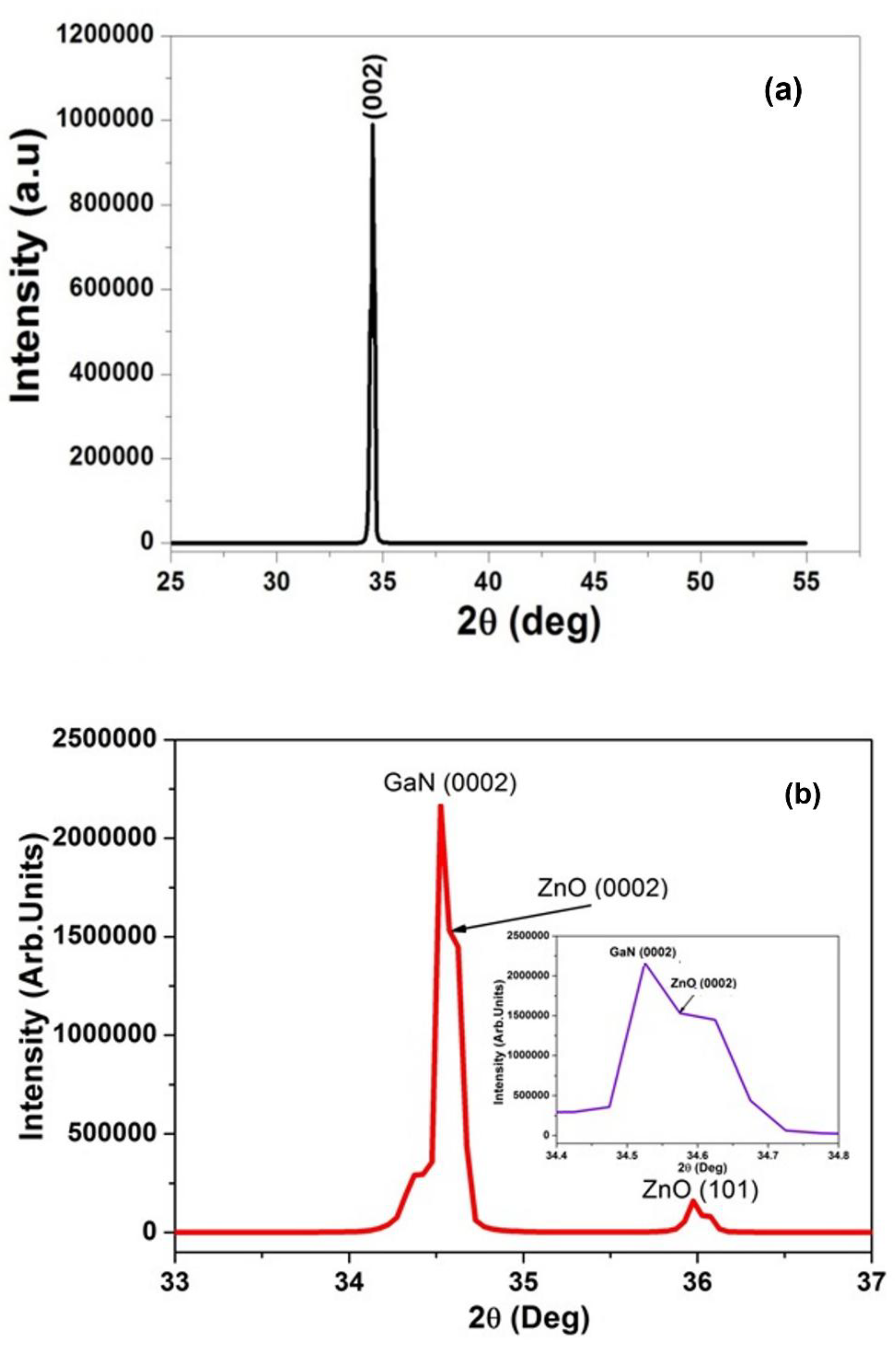
Figure 4.
FESEM images of pure ZnO thin film on deposited on (a) pristine and (b) porous GaN substrates. (c) FESEM image of N-ZnO film on porous GaN.
Figure 4.
FESEM images of pure ZnO thin film on deposited on (a) pristine and (b) porous GaN substrates. (c) FESEM image of N-ZnO film on porous GaN.
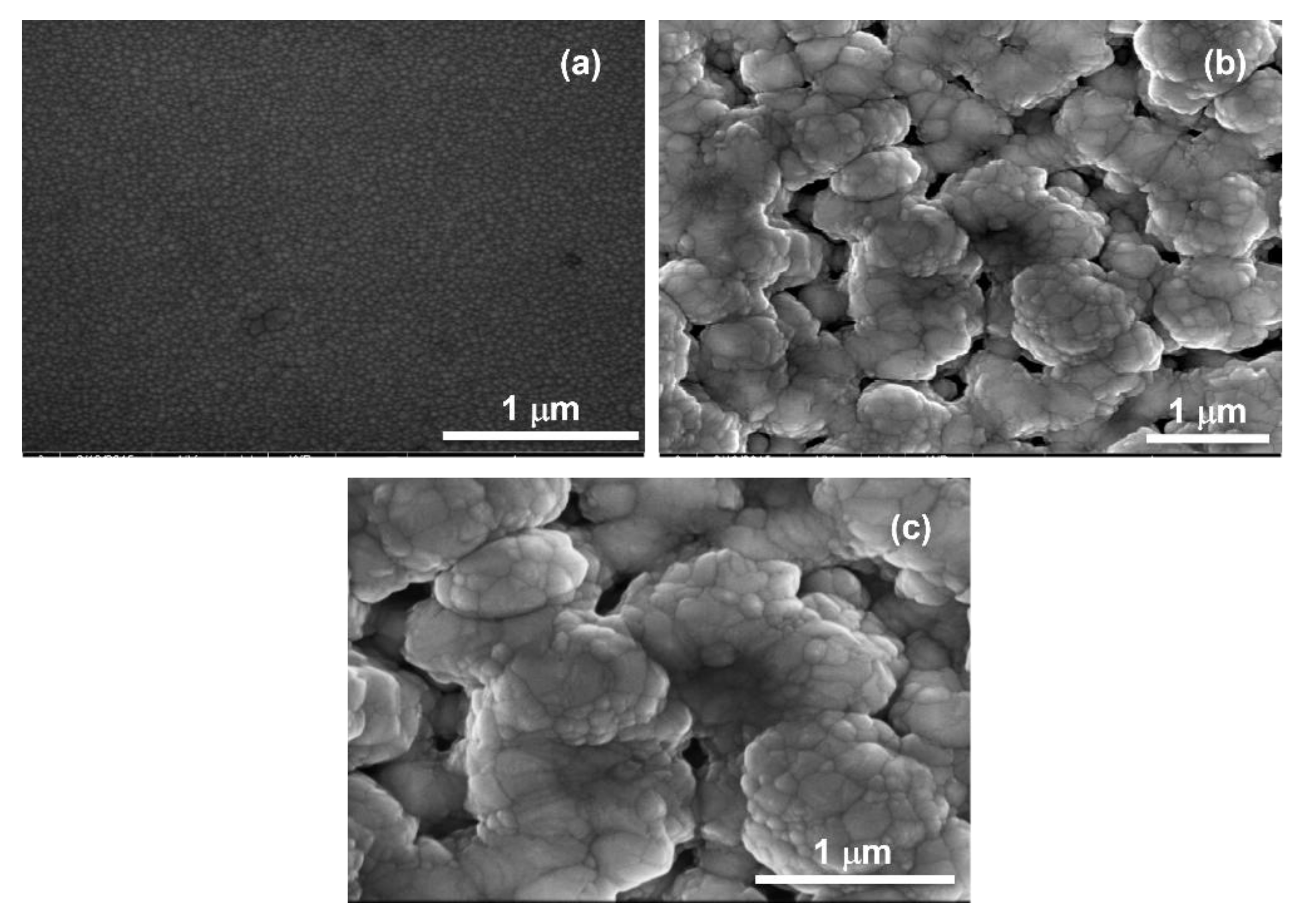
Figure 5.
AFM topography of the ZnO thin films. (a) Pure ZnO deposited on pristine and (b) on porous GaN substrate. (c-g) Nitrogen doped ZnO films on porous GaN substate with different nitrogen doping. Sccm- Standard denotes cubic centimeters per minute, refers to the nitrogen gas flow rate, doping gas. RMS denotes, root mean square value of surface roughness.
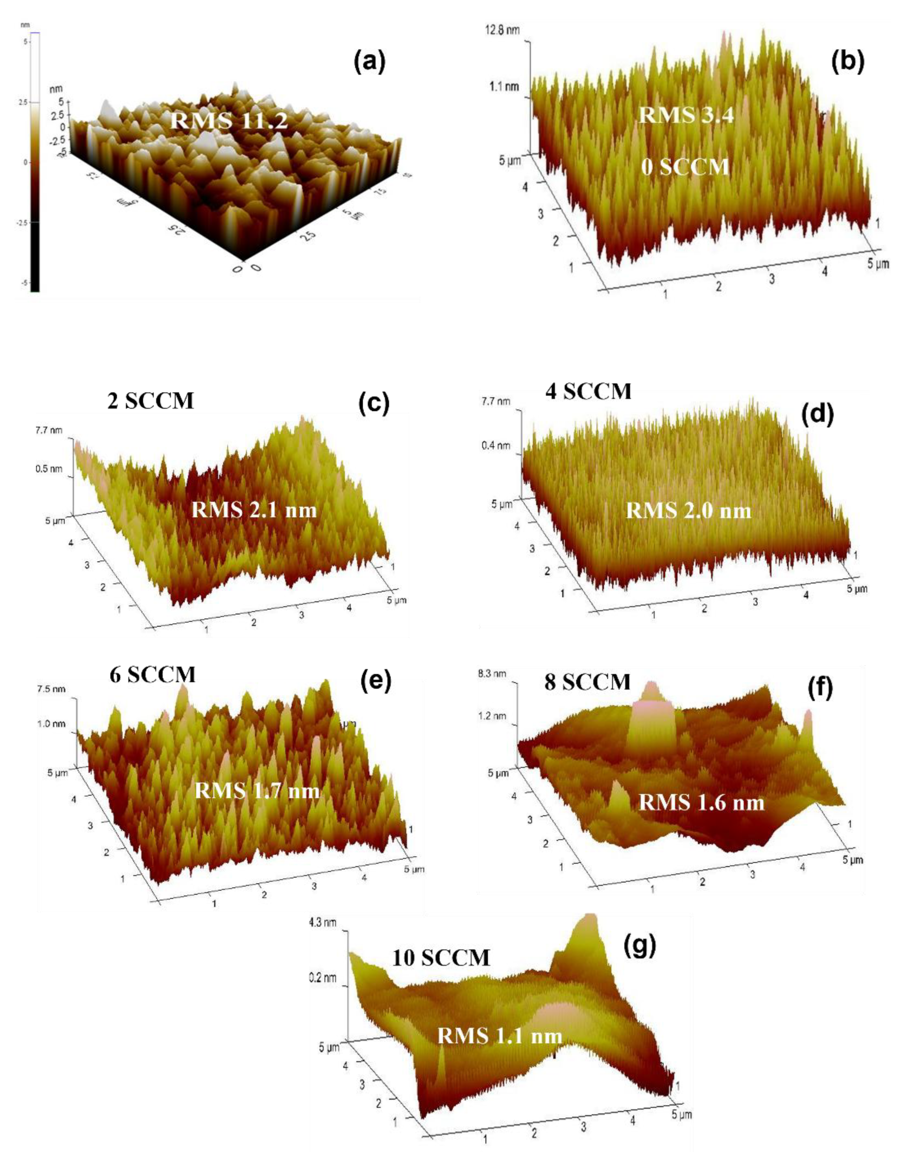
Figure 6.
Photoluminescence spectrum of pure ZnO thin films deposited on pristine and porous GaN substrates.
Figure 6.
Photoluminescence spectrum of pure ZnO thin films deposited on pristine and porous GaN substrates.
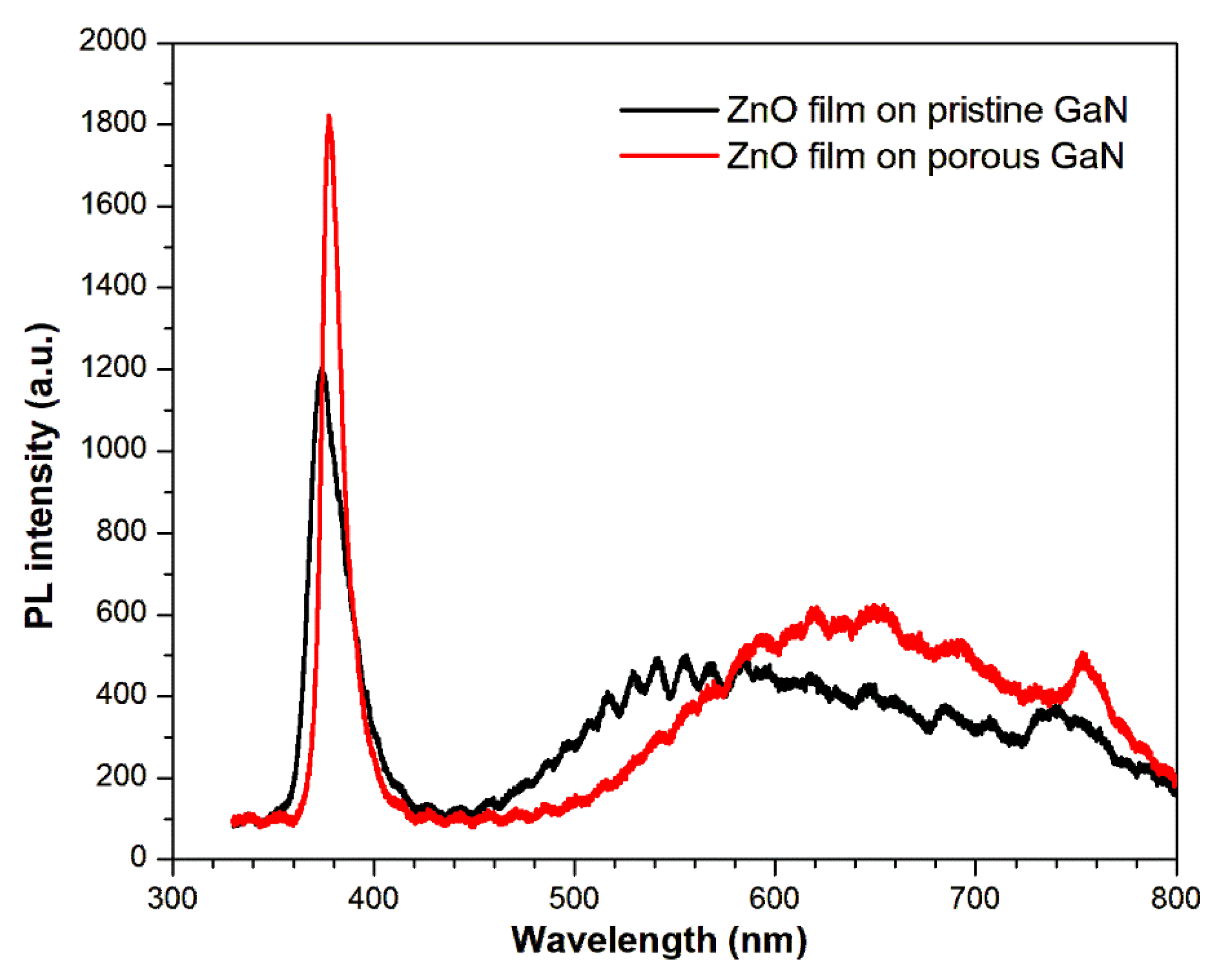
Figure 7.
UV-Visible transmittance spectra of pure ZnO and N-ZnO films on GaN template.
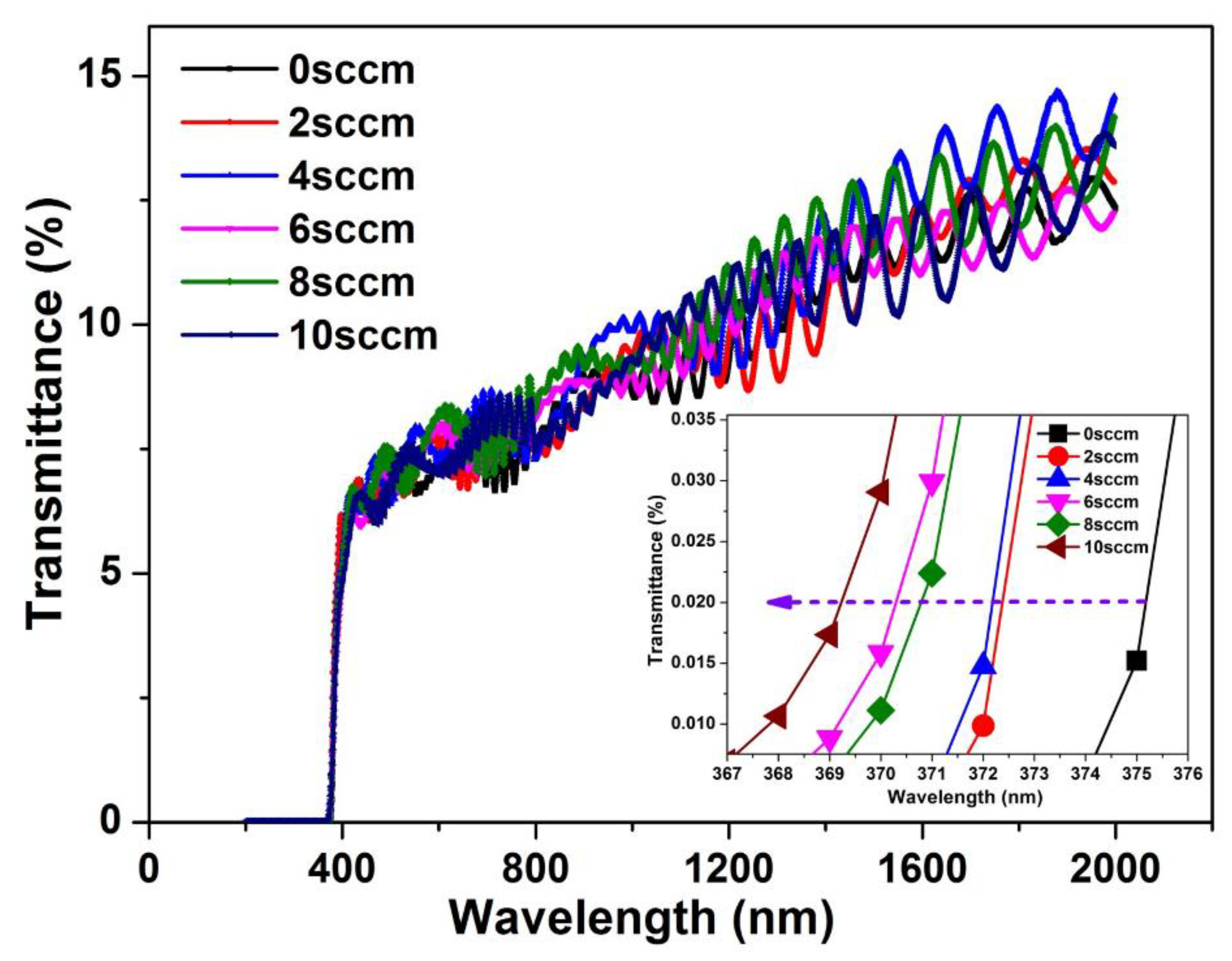
Figure 8.
Electrical properties of pure ZnO and N-ZnO films on GaN substrate. Electrical resistivity, carrier concentration and carrier mobility are plotted together in a single graph for comparison.
Figure 8.
Electrical properties of pure ZnO and N-ZnO films on GaN substrate. Electrical resistivity, carrier concentration and carrier mobility are plotted together in a single graph for comparison.
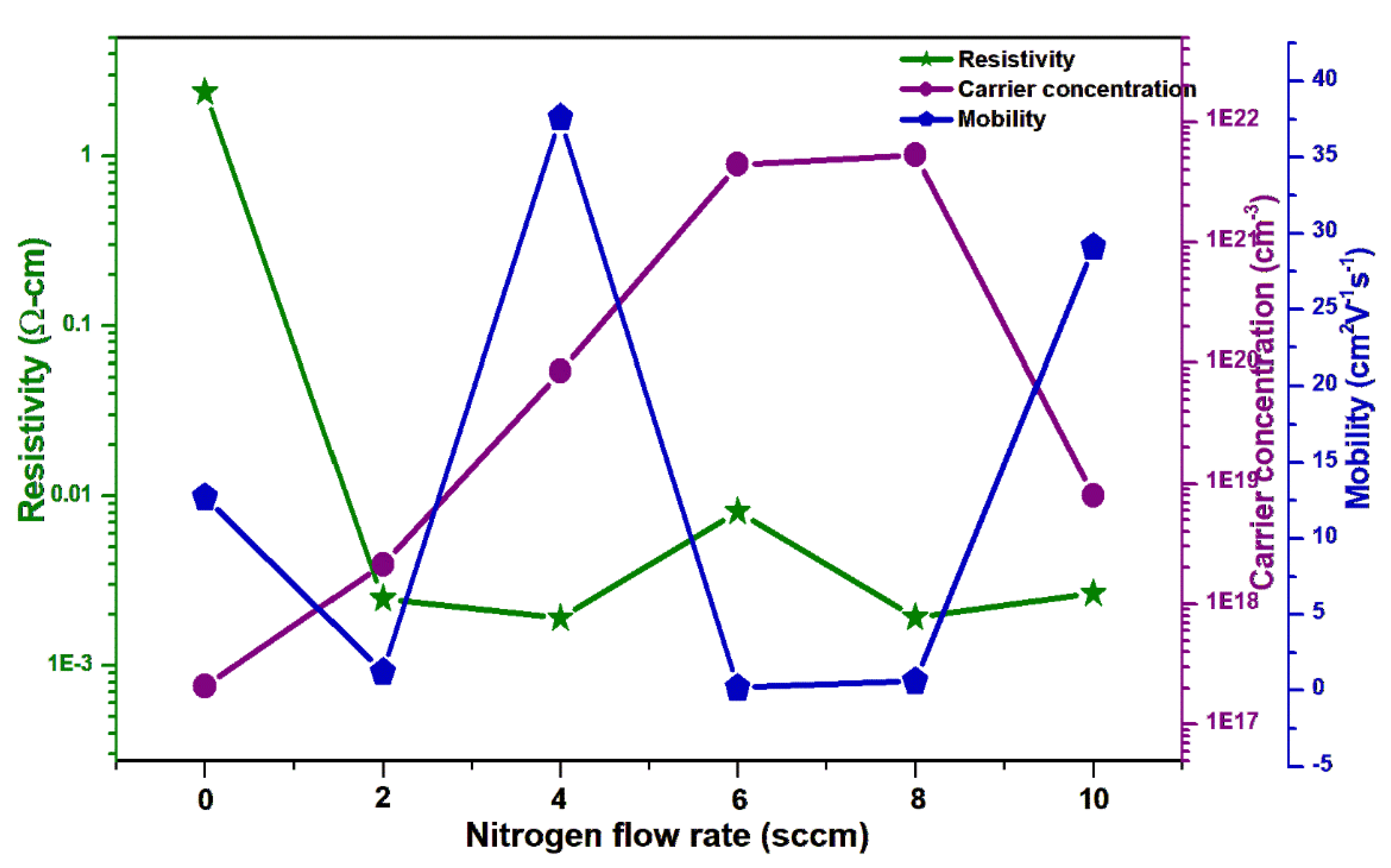

Table 1.
Optimized growth parameters for the deposition of ZnO films on GaN substrates.
| Growth Parameters | Experimental values |
|---|---|
| Substrate | Unintentionally doped GaN (n-type) |
| Metal oxide target | ZnO ceramic (99.999%) |
| Base Pressure | 3.0 x 10⁻⁵ milli bar |
| Working Pressure | 2.0 x 10⁻² milli bar |
| Substrate Temperature | Room temperature (no intentional substrate heating ) |
| Argon gas (atmosphere) | 10 sccm |
| Nitrogen gas (doping) | 2 sccm, 4 sccm, 6 sccm, 8 sccm and 10 sccm respectively. |
| Radio frequency (RF) sputtering power | 150 W |
Table 2.
Root mean square (RMS) values from AFM images of ZnO films on GaN substrate, and carrier concentration and mobility obtained from the Hall measurements of pure and N-ZnO film samples.
Table 2.
Root mean square (RMS) values from AFM images of ZnO films on GaN substrate, and carrier concentration and mobility obtained from the Hall measurements of pure and N-ZnO film samples.
| Film Sample | Nitogen gas flow (sccm) | RMS values on non-porous GaN (nm) | RMS values on etched porous GaN (nm) | Carrier concentraion (cm−3) | Carrier mobility (cm2V−1s−1) |
|---|---|---|---|---|---|
| Pure ZnO | 0 sccm | 11.2 | 3.4 | 4.71 × 10¹⁷ | 13.15 |
| N-doped ZnO | 2 sccm | - | 2.1 | 2.12 x 10¹⁸ | 2.5 |
| N-doped ZnO | 4 sccm | - | 2.0 | 8.54 x 10¹⁹ | 37.5 |
| N-doped ZnO | 6 sccm | - | 1.7 | 4.40 x 10²¹ | 1.0 |
| N-doped ZnO | 8 sccm | - | 1.6 | 5.29 x 10²¹ | 1.7 |
| N-doped ZnO | 10 sccm | - | 1.1 | 7.99 x 10¹⁸ | 29.8 |
Disclaimer/Publisher’s Note: The statements, opinions and data contained in all publications are solely those of the individual author(s) and contributor(s) and not of MDPI and/or the editor(s). MDPI and/or the editor(s) disclaim responsibility for any injury to people or property resulting from any ideas, methods, instructions or products referred to in the content. |
© 2025 by the authors. Licensee MDPI, Basel, Switzerland. This article is an open access article distributed under the terms and conditions of the Creative Commons Attribution (CC BY) license (http://creativecommons.org/licenses/by/4.0/).
Copyright: This open access article is published under a Creative Commons CC BY 4.0 license, which permit the free download, distribution, and reuse, provided that the author and preprint are cited in any reuse.


