1. Introduction
Significant efforts are being made to reduce the operating expenses (OPEX) of Concentrated Solar Power (CSP) systems [
1]. One key challenge is the performance of solar reflectors/mirrors, which is compromised by soiling [
2,
3]. Restoring the specular reflectivity of these mirrors requires large amounts of water [
4], and the cost of cleaning procedures directly impacts the levelized cost of energy (LCOE) produced by CSP plants [
5].
Among the various strategies to address this issue, the most effective involves the development of solar mirrors coated with thin, transparent, self-cleaning films. These coatings allow for significantly reduced water consumption during cleaning, leading to considerable cost savings, particularly in regions with high labor or resource costs, such as desert areas [
6].
Additionally, self-cleaning coatings play a crucial role in maintaining the cleanliness of all types of solar mirrors while resisting environmental degradation over time, without compromising optical transparency or reflectivity [
7]. Consequently, an emerging trend for ensuring the long-term performance of solar mirrors is the integration of autonomous and intelligent operational quality control systems, like those already being implemented in the photovoltaic sector [
8,
9,
10].
Providing a solar field with intelligence and automating O&M (Operations and Maintenance) processes requires the ability to monitor the dirt level or detect failures in individual mirrors (or even the entire field), enabling on-demand cleaning or component replacement [
11]. Practically, this could be achieved by adding commercial sensors to the mirrors. However, this approach would be costly and inefficient, as there are no commercial sensors currently suitable for use on solar mirrors. It’s important to remember that solar mirrors have strict optical requirements, are exposed to outdoor conditions, and, even in medium-sized solar plants, are found in large quantities [
12]. To date, no commercial sensor-equipped mirrors exist, only patented prototypes that incorporate scattering sensors into the mirror design [
13]. If a layer of the existing solar mirrors—such as the exposed layer—were made sensitive to soiling (or other specific parameters), it would allow for monitoring of their performance. This has motivated us to explore the integration of sensing thin films directly into the mirror structure.
In our previous work [
14], we demonstrated that the wetting properties of solar mirrors can be modified by applying transparent auxetic metamaterials to reflector surfaces using scalable processes, with the goal of reducing water consumption in cleaning procedures. Auxetic aluminum nitrides, deposited via sputtering on metallized low-iron glass, have been proposed as an ideal self-cleaning solution for back-surface mirrors. These coatings are transparent, hydrophobic, versatile, and can be applied to large substrates using cost-effective and scalable techniques.
But can these coatings be further engineered to meet additional functional requirements? This study seeks to answer that question. Our objective is to develop self-cleaning meta-materials that can also function as sensors to detect mirror performance failures caused by dust accumulation, excessive humidity, or other critical factors such as structural damage, aging, corrosion, and erosion. Through a dedicated electronic interface and IoT integration, these materials could provide real-time data on soiling levels and the overall functionality of individual components or the entire solar field.
Regarding aluminum nitrides, it is well known that thin films exhibit piezoelectric behavior when they crystallize in the hexagonal phase and grow perpendicularly to the substrate along the c-axis [
15].
Piezoelectric phases develop an electric dipole when the mechanical strain is applied to them. All dipoles add up over the entire material and produce a net polarization that results in electric field generation, that can be piezo-electrically transduced to electric voltage and current and hence detected.
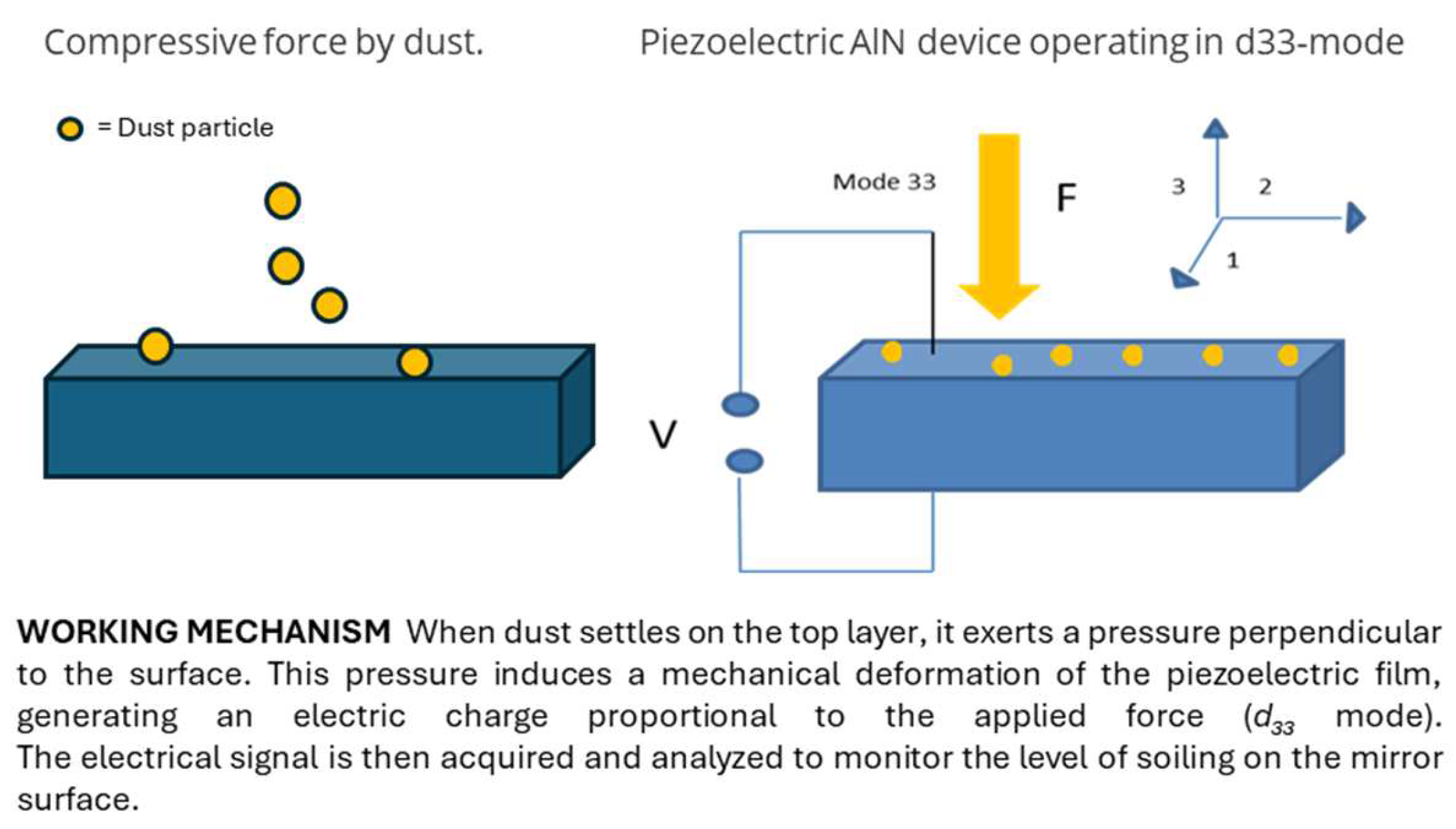
In other terms, if we coat a solar mirror with a piezoelectric material, we can turn it into a dust sensor. In desert environments, where dust conditions are extreme, the amount of dust that accumulates on a solar mirror can be significant. In regions like the Sahara or the Middle East, dust deposition rates range from 10 to 100 g/m² per day, with an average of about 1.5 kg/m² over the course of a month [
16]. This dust accumulation exerts pressure on the surface of the mirror, which can be detected by the piezoelectric material as an electrical signal.
The main challenge in this context is that dust does not accumulate uniformly. On a relatively small area, such as 1 cm², the piezoelectric signal generated by dust pressure would be very small, on the order of picovolts (pV), which is too low to be easily detectable by standard sensors. However, by increasing the sensitive area to 1 m², the generated signal increases significantly, reaching about 10 microvolts (µV), which is much more detectable than the signal from a smaller area. The importance of distributing sensing in this case is crucial. A larger sensitive area not only amplifies the piezoelectric signal enough to surpass the noise threshold (typically in the nanovolt range) but also allows for more precise monitoring of the entire surface of the mirror, averaging out localized pressure variations caused by dust. A larger surface area better distributes pressure fluctuations, improving the stability and reliability of the detection system.
In summary, by using a larger sensitive area and optimizing the piezoelectric material properties, measurable signals can be obtained even under harsh desert conditions, where dust accumulates rapidly and unevenly. This dual strategy of enhancing piezoelectric material properties and defining an effective device architecture is crucial for achieving robust, measurable signals in distributed dust sensing.
In this work, we focus on maximizing the piezoelectric effect of the material in the form of a thin film. The goal is to optimize the piezoelectric properties to generate a strong and measurable signal in response to dust accumulation. The study aims to enhance the material’s performance by fine-tuning its composition and structure to achieve the highest possible sensitivity. In a future study, we will investigate the optimal device area to further improve the sensor’s efficiency and performance, ensuring that the sensitive skin can reliably detect dust accumulation across the entire surface of the solar mirror.
In particular, the first step of fabrication of thin AlN films by means of reactive sputtering processes has been directed to maximize piezoelectric coefficients of the material, in manner that dust deposition (and hence the soiling of the surface) can be treated as mechanical strain and in such way detected, preserving at the same time all requirements of self-cleaning and optical clarity in the full solar range.
Moreover, considering the use of piezoelectricity to give sensing properties for detecting soiling on a solar mirror’s surface, and recognizing that zinc oxide (ZnO) is another transparent piezoelectric material [
17], sputtered ZnO-based inorganic composites have been investigated. The decision to incorporate zinc oxide into a transparent, insulating matrix was made to preserve the optical properties of solar mirrors, especially their refractive index. In this case, our goal was to evaluate both the piezoelectric and electrical conductivity properties of these composites, aiming to create a versatile sensing skin capable of providing different outputs for potential neural sensor architectures [
18]. Additionally, such a system could be integrated into multimodal sensing systems designed to detect various stimuli, including light, pressure, and chemical changes, ultimately contributing to more accurate, brain-like behavior in artificial neural networks [
19]. To achieve this, the sputtering process for ZnO-based composites was optimized to detect piezoelectric behavior, even when ZnO is dispersed within an insulating matrix, while also assessing the electrical properties of various composite films, all while maintaining the optical transmittance across the full solar spectrum and the self-cleaning capabilities of the material.
2. Materials and Methods
Aluminum nitrides were fabricated by means of sputtering deposition, using the proprietary multi-cathode sputtering custom built apparatus, named ENEA2, equipped with process chamber and load lock chamber. ENEA2 is the apparatus by which they have been developed, patented and transferred to the international industry key technologies in the field of selective thin-film solar coatings for receiver tubes [
20]. The mirror substrate has been positioned in front of the target in a planar configuration and the fabrication process has been a reactive sputtering at Ar+N
2 pressure of 3 Pa with power supplied to Al cathode of 1800W for auxetic phase and of 0.3 Pa with power supplied to the target of 3600W for piezoelectric phase.
Zinc oxide-based nanocomposites were fabricated by means of a solid-state reaction between thin films of ZnO and Silicon obtained by means of a planar magnetron multi-cathode sputtering apparatus by Material Research Corporation Mod. MRC 643. Boron doped Si and undoped ZnO sputter targets (dimensions: H = 38 cm and L = 12 cm) were used coupled with bi-polar pulsed DC and RF generator, respectively. Sputtering processes have been carried out at pressures of 2.0 Pa, starting from a base vacuum of about 2 x 10⁻⁴ Pa.
The solid-state reaction was carried out in a vacuum at temperatures between 450 °C and 560 °C, with reaction times ranging from 3 to 6 h for conductive samples containing ZnO micro- or nano-domains, respectively. Solar mirrors substrates have been purchased by Società Vetraria Biancaldese Spa.
UV-VIS-NIR analysis has been performed using a double beam Perkin-Elmer mod. Lambda 900 instrument, equipped with a 15 cm integrating sphere to measure global spectral reflectance and transmittance. The optical bandgap of phases constituting different composites has been defined by UV-VIS-NIR reflectance and transmittance measurements, by means of Tauc’s plot method [
18], assuming for ZnO and silicates a direct transition. The assumption of a direct transition for ZnO and zinc silicates is based on the known electronic structure and optical properties of these materials. ZnO, being a wide-bandgap semiconductor, exhibits a direct bandgap, which allows for efficient absorption of light and direct electronic transitions. Similarly, zinc silicates are considered to follow a direct bandgap transition due to their crystalline structure and similar electronic characteristics to ZnO. This assumption is supported by previous studies, where direct transitions have been observed in these materials through optical characterization techniques [
21,
22].
The thickness of each sample was measured mechanically using a Tencor P-10 surface profiler.
The Static Water Contact Angle (WCA) was measured with the direct optical method of drop-shape analysis, by means of the contact angle meter KRUSS DSA-100.
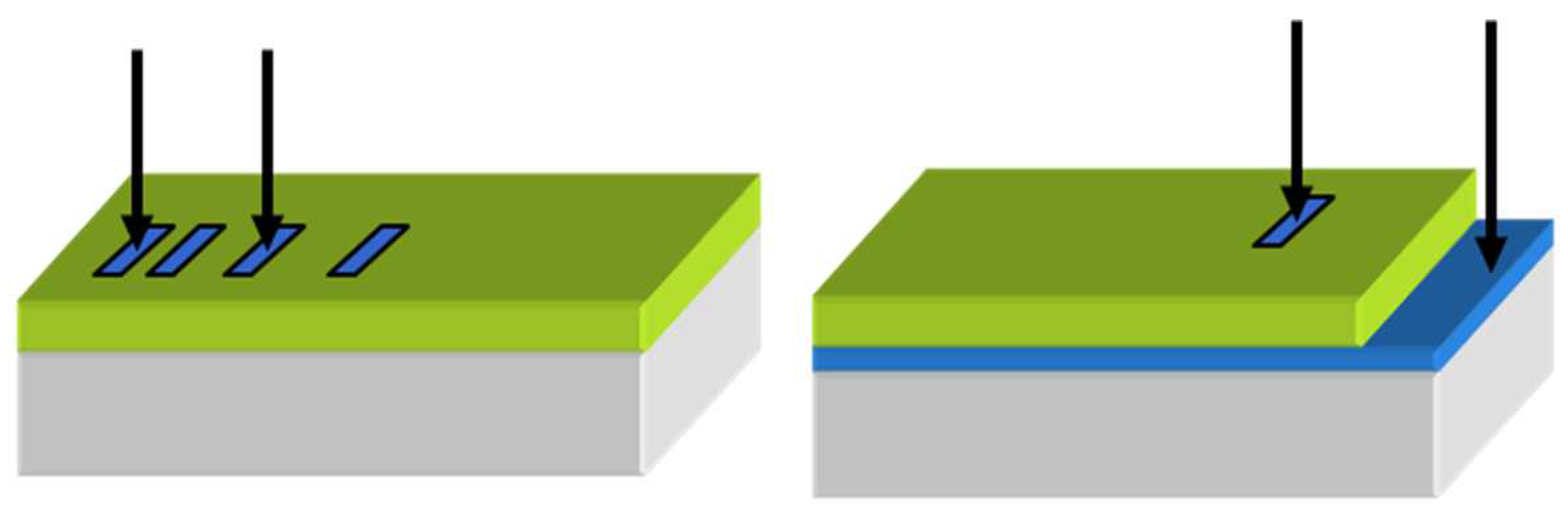
For testing electrical properties of different materials two main configurations have been utilized: planar and vertical. The first is made by means of electrical Aluminum contacts evaporation onto the film (with a known and regular geometry) and the second is made by interposing the film between a metallic sputtered thin W layer and an evaporated metallic contact, as shown in
Figure 1.
For the W deposition the chamber has been filled with 200sccm of Argon at a pressure of 0.4Pa. The DC power applied was 2500W, speed of translation was 500mm/min, and the number of scans was 4.
X-ray diffraction analysis was performed using a Philips Panalytical X’ PERT PRO MRD diffractometer working with CuKα radiation (λ = 1.54059 nm). The glancing incidence configuration was used to obtain high sensitivity to the film structure: the measurements were collected at incidence angles of 0.5° and 1° and using a scan range of 10°–100° (2θ).
Microstructural investigation of ZnO composites on Si(100) were performed by TEM using a JEOL JEM 2010F TEM operating at 200kV acceleration voltage and equipped with a field emission gun. The system was imaged in cross-section and in plane-view using diffraction contrast, selected area electron diffraction (SAED) and high-resolution TEM (HRTEM. Standard TEM sample preparation was used. Optical measurements were performed at room temperature with an Agilent 8453E ultraviolet-visible spectrometer with a resolution of 1 nm.
The piezoelectric response d33 of fabricated samples has been measured by means of a D33meter POLIK.
3. Results and discussion
Starting from the previous results about auxetic aluminum nitrides developed as ideal for substituting alumina as BSM self-cleaning skin, here it has been explored the possibility of conferring sensing properties to this material, by utilizing its piezoelectric properties combined to the distributed sensing of a large area of deposition. When dust accumulates on a solar mirror, it exerts pressure on the surface. This pressure generates a piezoelectric signal in the mirror’s aluminum nitride coating, as shown in
Figure 2. With a large area, the total pressure from dust accumulation is distributed over a large surface, resulting in a signal which is several orders of magnitude larger than the signal from a smaller area. Clearly, the maximization of piezoelectric behavior is crucial for exploiting the distributed sensitive performance.
So, the thin film AlN fabrication by means of reactive sputtering process has been directed to maximize the piezoelectric strain constant (d33) of the material, that can be correlated to dust deposition (considered as an applied force), and hence to the soiling of the surface.
From a structural perspective, the
d₃₃ piezoelectric coefficient of sputtered AlN films is highest when the material crystallizes in the hexagonal wurtzite phase and when its crystallites grow with c-axis orientation [
23]. The crystallographic phase and orientation are closely tied to the deposition technique used. Aluminum nitride thin films can be deposited using chemical vapor deposition (CVD), molecular beam epitaxy, or sputtering in either DC or AC mode [
24]. The advantage of the selected reactive sputtering process is that it enables room-temperature deposition, with c-axis orientation tunable through various process parameters, such as the
discharge power/pressure ratio and the
Ar/N₂ gas flow ratio.
Even when sputtered thin films exhibit mixed orientations, it is still possible to maximize piezoelectric response. This is because, within the 10–200 nm thickness range required to ensure optical clarity across the full solar spectrum for self-cleaning purposes, the coatings naturally exhibit an intrinsic anisotropy due to their polycrystalline structure.
Extensive experimental work has been dedicated to optimizing process conditions to balance optical transmittance, self-cleaning wettability (contact angle, WCA), and the maximization of the piezoelectric coefficient in sputtered AlN thin films.
Table 1 reports the defined magnetron sputtering conditions and WCA, of auxetic, amorphous and piezoelectric AlN self-cleaning coatings.
The measured contact angles (WCA) are all greater than 90°, confirming self-cleaning behavior compared to uncoated mirrors. It should be noted that in a BSM, the layer exposed to air is alumina, which typically has contact angles around 40°. Therefore, replacing the alumina layer on the glass with an AlN layer, as previously explained, ensures self-cleaning properties, allowing the mirrors to be washed with a reduced amount of water [
25].
Once the self-cleaning effect is preserved, we can now focus on the piezoelectric properties. To maximize the piezoelectric behavior, process parameters were adjusted until the film became amorphous, followed by further modifications involving a significant reduction in process pressure and an increase in the power supplied to the aluminum target. Both conditions indicate a more energetic process, which promotes the coalescence of fine columnar wurtzite grains into larger ones.
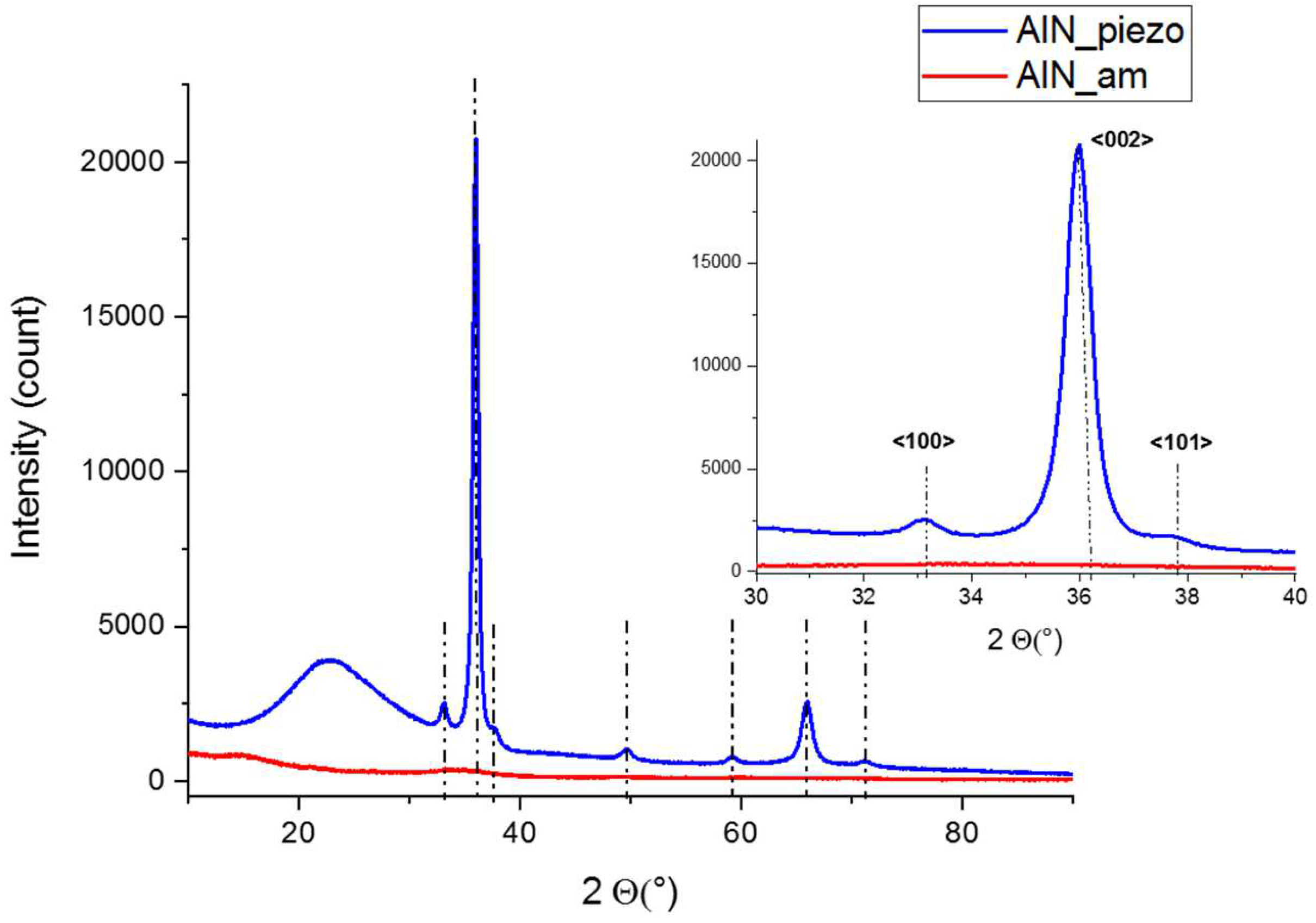
Figure 3 presents the XRD spectra of both amorphous and piezoelectric films.
A greater thickness was chosen to enhance the piezoelectric coefficients. However, it is important to note that further increasing the thickness could compromise the coating’s optical clarity across the full solar spectrum.
Increasing the thickness of the coating beyond a certain point may lead to light scattering and absorption, which would reduce the transparency of the film. This would be particularly problematic in the context of maintaining optical clarity across the full solar spectrum, as any reduction in transmittance could negatively impact the overall efficiency of solar mirror systems. Therefore, while thicker films can improve piezoelectric properties, the trade-off between thickness and optical clarity must be carefully balanced to ensure optimal performance for both the self-cleaning and reflective functions of the mirror.
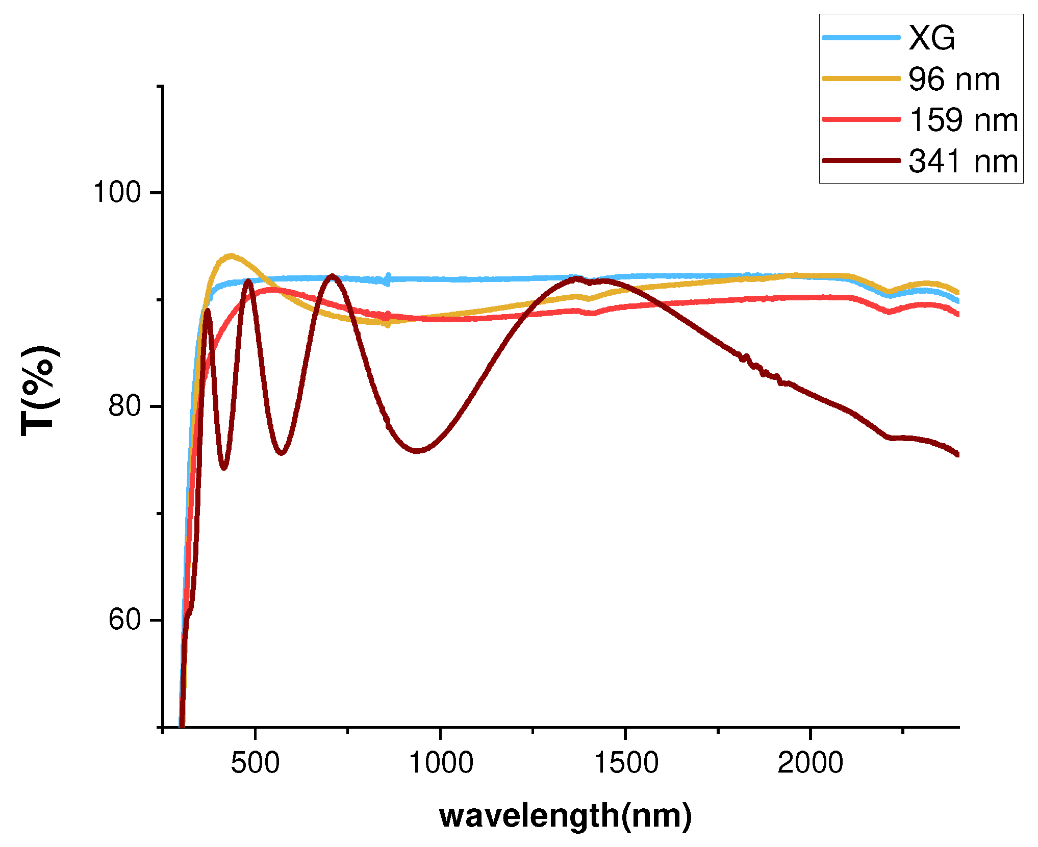
To support this, it is useful to observe the UV-VIS-NIR transmittance trend of sputtered AlN thin coating films shown in
Figure 4.
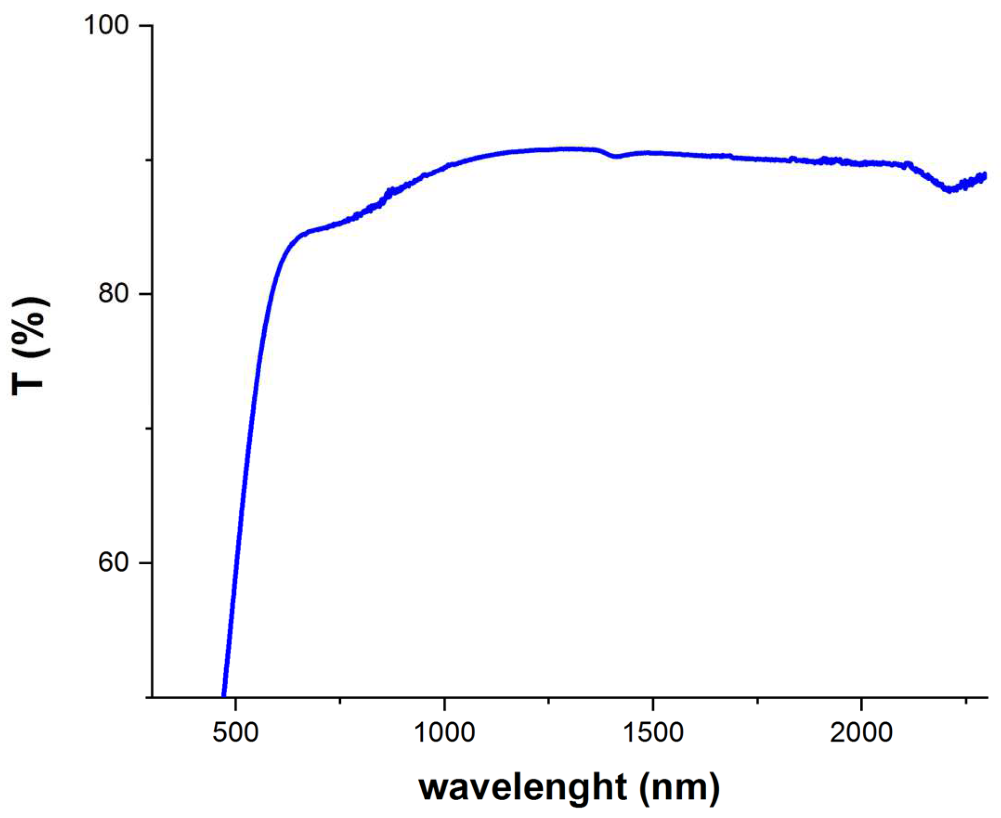
Starting with the XG glass substrate, one can observe the difference in transmittance of the films at varying thicknesses where it should be taken into account that the optimal optical behavior is the one closest to that of the uncoated substrate.
The piezoelectric coefficient d₃₃ of the fabricated samples was measured, and for the selected sample AlNpiezo, it was found to be 1.8 pC/N under an applied force of 5N. This promising value enables the use of this material as a piezoelectric soiling transducer, advancing the development of a soiling-detecting solar mirror skin.
Another useful property for detecting solar mirror failures in different configurations is a change in the coating’s electrical conductivity. The key idea is that a
sensitive skin should be multifunctional, meaning it should provide different outputs, similar to the smart materials used in the building sector [
20].
In this way the future step of fabricating a neural network of devices starting from selected materials can be simplified choosing properties that can be easily integrated.
Aluminum nitrides are well known for their insulating properties, but ongoing studies are exploring doping with metallic particles to develop resistive composites capable of altering their electrical resistivity in response to various failure-related inputs.
Following this approach, we have also tested another material as a potential sensitive solar mirror skin: a family of inorganic composites containing different amounts of zinc oxide (ZnO). These composites exhibit both piezoelectric properties—due to the combined effect of the thin film’s overall anisotropy and ZnO’s intrinsic piezoelectric behavior—and resistive properties, resulting from the presence of conductive crystalline ZnO islands embedded within an insulating silicate matrix. In other terms, each composite can be optimized for a particular task (detecting failure, sensing soiling, monitoring relative humidity and so on) depending on its specific electric behavior.
The fabrication of these composites was achieved through a solid-state reaction occurring at 450–560°C between sputtered ultra-thin layers of silicon and zinc oxide. This process leads to the formation of ZnO crystalline domains of different sizes within a transparent silicate matrix, which also provides self-cleaning capabilities.
Table 2 reports the defined experimental conditions and wetting contact angle, WCA, of ZnO composites self-cleaning coatings.
Before the reaction, the samples appear opaque due to the stratification of the reagents. However, after undergoing the solid-state reaction—an annealing process at temperatures ranging from 450 to 560°C—optical transmittance in the desired solar range is achieved.
In
Figure 5 the optical transmittance of sample C1-4 has been reported.
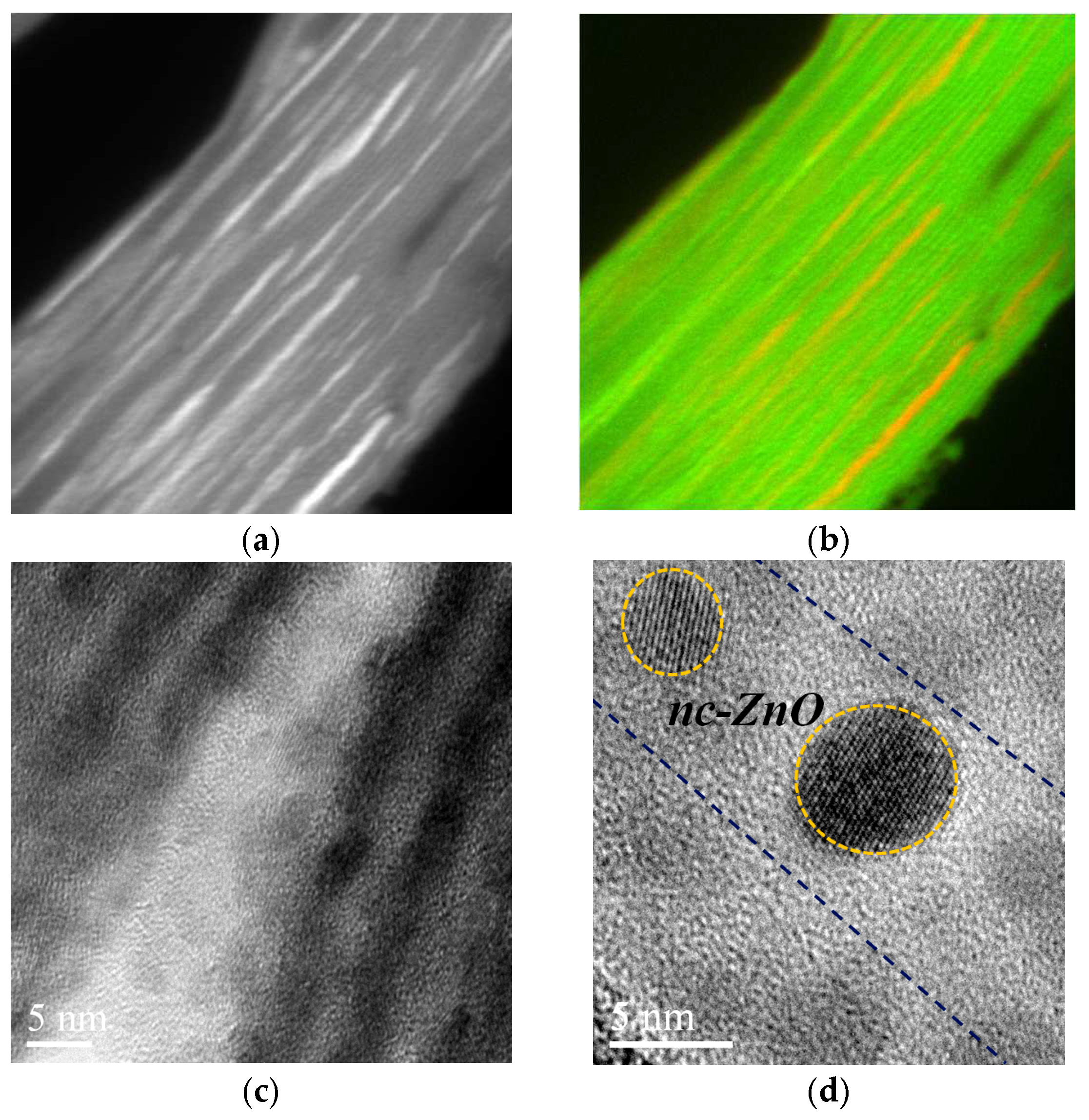
TEM investigations, reported in
Figure 6 confirm the presence of crystalline ZnO domains embedded in amorphous silicates.
Alternate regions appear in terms of different brightness and by energy electron loss spectroscopy (EELS) we verified they are correlated to sheet silicate layer’s structure consisting of distorted tetrahedra SiO4 sheet (clear regions) and distorted octahedron MO6 sheet (dark regions), where M=Zn. Inside MO6 layers crystalline two ZnO nanoaggregates appear, whose interplanar spacing gave larger average value (2.57 Å) for both the nanoaggregates, very close to the value (2.603 Å) of the lattice parameter in (002) direction of the ZnO crystalline structure (wurzite).
Electrical characterization has been performed for measuring lateral and vertical resistivity in the configuration previously described and reported in
Table 3.
Low values for lateral resistivity (samples C1-4, C85-4, C85-45, C85-45b) could be attributed to the presence of unreacted ZnO thin layers (crystalline phase with optical band gap determined by means of Tauc’s plot method are in the range 3.2 – 3.4 eV) giving a quasi-metallic transport mechanism. Regarding vertical resistivity, all the samples show middle-high values that can be justified in terms of larger/smaller interposed silicate layer thicknesses (or in terms of larger/smaller vertical spacing between ZnO domains).
In other terms, the observed electrical anisotropy is due to the presence of conductive p-type ZnO domains in the plane of the film layered with the insulating matrix in the vertical direction. When dimensions of the ZnO domains are reduced to the nanometric range the conductivity drops, because prevails the insulation property of silicate matrix.
The piezoelectric coefficient d33 of fabricated samples has been measured and for the selected sample C1-4 it results to be -0.8 pC/N under a 5N applied force. This value combined with the different lateral and vertical electrical conductivity enables the utilization of such material as sensitive skin of solar mirrors.
4. Conclusions
Self-cleaning transparent metamaterials have been designed, fabricated, and characterized as solar mirror coatings with potential sensor capabilities for various parameters, including dust accumulation, humidity, erosion, aging, and failure detection.
AlN-based coatings have been explored as soiling sensors due to their piezoelectric properties. Dust accumulation applies pressure on the coated mirror surface, which the piezoelectric material detects as an electrical signal. Distributed sensing plays a crucial role in this approach. Expanding the sensitive area not only enhances the piezoelectric signal beyond the noise threshold but also enables more precise monitoring of the entire mirror surface soiling, compensating for localized pressure variations caused by dust. Experimental work has focused on optimizing sputtering process conditions to maximize piezoelectric performance, laying the groundwork for future research on the devices testing on field and sensitive area optimization.
ZnO composites have been investigated as resistive sensors, capable of altering their electrical conductivity in response to failure events. Experimental efforts have focused on defining the conditions for a solid-state reaction between sputtered silicon and zinc oxide reagents. This reaction generates a family of coatings with different concentrations of conductive micro- and nano ZnO domains, exhibiting anisotropic electrical resistivity. If a failure event (such as cracking, delamination, or thermal stress) occurs, it might alter the electrical conductivity of the material, providing a detectable signal.
This innovative approach integrates self-cleaning properties with electrical functionality while maintaining optical transparency, demonstrating promising potential for distributed sensing applications in solar coatings. The proposed materials are cost-effective, scalable, and versatile, making them well-suited as sensitive solar reflector skins, whose adoption could significantly reduce field maintenance costs in solar power plants. while advancing the first step toward the smartization of CSP technology.
Author Contributions
Conceptualization, A.C; methodology, A.C. and E.G; software, E.G.; validation, A.C..; formal analysis, A.C; investigation, A.C. and E.G.; resources, A.C..; data curation, E.G.; writing—original draft preparation, A.C; writing—review and editing, .C. and E.G.; visualization, E.G..; supervision, A.C..; project administration, A.C..; funding acquisition, A.C.. All authors have read and agreed to the published version of the manuscript.
Funding
This work was funded by the Italian Ministry of Environment and Energy Security through the “National Electric System Research” Programme – Project 1.9 “CSP/CST technology”, 2022-2024 implementation plan.
Conflicts of Interest
The authors declare no conflict of interest.
References
- Khan, M.I. , Gutiérrez-Alvarez R., Asfand F., Bicer Y., Sgouridis S., Sami G. Al-Ghamdi, Hussam Jouhara, M. Renewable and Sustainable Energy Reviews, A: Apostolos Pesyridis, Muhammad Farooq, The economics of concentrating solar power (CSP), 2024. [Google Scholar] [CrossRef]
- El boujdaini, l. , Mezrhab A., Moussaoui M.A., Carballo Lopez J.A., Wolfertstetter F. Sustainable Energy Technologies and Assessments, E: materials, 2022; 53. [Google Scholar] [CrossRef]
- Heimsath, A. , Heck, M., Morin, G., Kiewitt, W., & Platzer, W. (2010). Soiling of aluminum and glass mirrors under different climatic conditions and techno-economic optimization of cleaning intervals. Proceedings of the SolarPACES, Perpignan, France.
- Elsherif, H. , and H. M. Kandil. “Fully-automated cleaning systems for Photovoltaic panels and reflectors.” GUC Workshop on Renewable Energies and Smart Grid. 2011.
- Li, X. Zhao X., Li J., Li W., Xu N., Huang W. Analysis of life-cycle levelized cost of electricity for tower solar thermal power Autom Electr Power Syst, 2015, 39, 84-88.
- Adak, D. , Bhattacharyya, R., Barshilia, H.C., 2022. A state-of-the-art review on the multifunctional self-cleaning nanostructured coatings for PV panels, CSP mirrors and related solar devices. Renew. Sustain. Energy Rev. [CrossRef]
- Dahlioui, D. , Wette J., Fernández-García A., Bouzekri H., Azpitarte I. Solar Energy, 2022; -23. [Google Scholar] [CrossRef]
- Villasante-Corredoira, C. , Mabe-Alvarez, J., Les Aguerrea, I., Peña-Lapuente, A., Sanchez-Gonzalez, M., Lopez, S.. SMARTCSP: INDUSTRY 4.0 APPROACH FOR AN EFFECTIVE CONCENTRATED SOLAR POWER (CSP) COST REDUCTION. DYNA 2020, 95, 629-634. [CrossRef]
- Aghaei, M. , Kolahi, M., Nedaei, A., Venkatesh, N.., Esmailifar, S.., Moradi Sizkouhi, A.., Aghamohammadi, A., Oliveira, A..., Eskandari, A., Parvin, P., Milimonfared, J., Sugumaran, V. and Rüther, R. (2024), Autonomous Intelligent Monitoring of Photovoltaic Systems: An In-Depth Multidisciplinary Review. Prog Photovolt Res Appl. [CrossRef]
- M. Emamian, A. M. Emamian, A. Eskandari, M. Aghaei, A. Nedaei, A. M. Sizkouhi,and J. Energies, 2022; 15. [Google Scholar]
- Castaldo, A. , Gambale E., Vitiello G., Lanchi M.,Turchetti L. Proceedings of the SolarPACES 2022, 28th International Conference on Concentrating Solar Power and Chemical Energy Systems Advanced Materials, Manufacturing, and Components, 2022. [Google Scholar] [CrossRef]
- Boretti, A. (2018). Concentrated Solar Power Plants Capacity Factors: A Review. In: Dai, L., Jazar, R. (eds) Nonlinear Approaches in Engineering Applications. Springer, Cham. [CrossRef]
- WO 2018/069558 A1 Mirror for a solar reflector, method of mirror assembly and management system in a solar field, FUNDACION CENER CIEMAT, 2018.
- Castaldo, A. , Gambale E., Vitiello G., “Aluminum Nitride Doping for Solar Mirrors SelfCleaning Coatings. Energies 2021, 14, 6668. [Google Scholar] [CrossRef]
- McKinlay, M. , Fleming L., García M. P., L. N. Sierra, P. V. Castro, D. Araujo, B. J. García, D. Gibson, C. G. Nuñez, On the Piezoelectric Properties of Zinc Oxide Thin Films Synthesized by Plasma Assisted DC Sputter Deposition. Adv. Mater. Interfaces 2024, 11, 2400252. [Google Scholar] [CrossRef]
- Ilse, K. , Micheli L. et al. Techno-Economic Assessment of Soiling Losses and Mitigation Strategies for Solar Power Generation. Joule 2019, 3, 2303–2321. [Google Scholar] [CrossRef]
- Li, Z. , Liu, J., & Zhang, Q. ZnO-based nanomaterials for brain-machine interface: Challenges and prospects. Nano Research 2021, 14, 17–32. [Google Scholar]
- Liu, H. , Wang, H., & Wu, Z. Multimodal sensing devices based on ZnO nanowires: A review of sensing mechanisms and applications. Journal of Materials Science 2018, 53, 1–17. [Google Scholar]
- Schmidgall, S. , Ziaei R., Achterberg J., et al. Brain-inspired learning in artificial neural networks: A review. APL Mach. Learn. 2024, 2, 021501. [Google Scholar] [CrossRef]
- Esposito, S. , D’Angelo A., Antonaia, A., Castaldo A., Ferrara M., Addonizio M.L., Guglielmo A. Optimization procedure and fabrication of highly efficient and thermally stable solar coating for receivers operating at high temperature. Applied Thermal Engineering 2016, 102, 91–107. [Google Scholar]
- Murayama, K. , Toyama T., Seiichi Miyazaki, Masataka Hirose. Fundamental absorption edge spectrum of ultrathin a-Si : H film in a-Si : Ha-Si3N4 : H multilayer obtained from luminescence excitation spectrum. Solid State Communications 1997, 104, 119–123. [Google Scholar] [CrossRef]
- S. Y. Ren, J.D. Dow, Thermal Conductivity of superlattices. Phys. Rev. B 1992, 45, 6492. [Google Scholar]
- F. Iriarte, J.G. Rodríguez, F. Calle, Synthesis of c-axis oriented AlN thin films on different substrates: A review. Materials Research Bulletin 2010, 45, 1039–1045. [CrossRef]
- J. Ohta, H. J. Ohta, H. Fujioka, M. Sumiya, M. Furusawa, M. Yoshimoto, H. Koinuma, M. 2000. [Google Scholar]
- Castaldo, A.; Gambale, E.; Vitiello, G.; Cara, G. Self-Cleaning Solar Mirror Coatings: From the Laboratory Scale to Prototype Field Tests. Appl. Sci. 2024, 14, 6669. [Google Scholar] [CrossRef]
- Iacona, F. , Bongiorno C., Spinella C., Boninelli C., Priolo F., JAP 2004 95, 3723-3732.
- Zhang, Wei, Smart Building Skin Design with Dynamic Climate Adaptability of Smart Cities Based on Artificial Intelligence, Advances in Multimedia, 2023, 2859195, 12 pages, 2023. [CrossRef]
|
Disclaimer/Publisher’s Note: The statements, opinions and data contained in all publications are solely those of the individual author(s) and contributor(s) and not of MDPI and/or the editor(s). MDPI and/or the editor(s) disclaim responsibility for any injury to people or property resulting from any ideas, methods, instructions or products referred to in the content. |
© 2025 by the authors. Licensee MDPI, Basel, Switzerland. This article is an open access article distributed under the terms and conditions of the Creative Commons Attribution (CC BY) license (http://creativecommons.org/licenses/by/4.0/).