Submitted:
27 February 2025
Posted:
03 March 2025
You are already at the latest version
Abstract
The properties of harmonic waves, carrying a longitudinal electric field and a space-charge density, made up of conduction electrons, are investigated in metals and semi-conductors with help of a classical analysis. The associated dispersion curve is worked out. These findings are further applied to unravel a novel second harmonic generation mechanism for an electromagnetic wave shone on a nanometric wire, with frequency ranging from the IF up to UV domain. The calculated efficiency in semi-conductors might be higher by 12 orders of magnitude than in metals. Observable predictions are made.
Keywords:
non linear optics
; plasmonics
1. Introduction
Second harmonic generation (SHG) at frequency has been initially investigated in case of an electromagnetic wave of frequency interacting with molecular dipoles, lacking inversion symmetry, but such that the energy difference between the electronic ground- and excited states, making up each dipole, is close to [1]. Therefore subsequent observation of SHG, over a broad frequency range, in bulk materials displaying conversely inversion symmetry[2,3] or at their surface [4,5], for which the incident light was coupled with valence and conduction electrons rather than molecules, was bound to require new interpretations. The corresponding hydrodynamic and quantum arguments were further extended to account tentatively for SHG data, measured in metallic samples [6,7,8] of nanometric ( nm) dimension. Remarkably those various explanations shared a common feature, since all of them dealt with conduction electrons coupled with an electromagnetic field [2,3,4,9,10,11], obeying Maxwell’s equations [12] and thence not allowing for 3-dimensional space-charge for some reason to be developed in the conclusion. Therefore this work is aimed at devising the first theory of space-charge waves in conducting materials. Its potential will then be illustrated by investigating SHG induced in samples of nanometric length. As a matter of fact SHG will turn out to stem from the quadratic term, showing up in the expressions of the drift current and the polarisation of conduction electrons. Actually space-charge solitons have already been invoked to account for the Gunn effect [13] and acousto-electric instabilities observed in piezoelectric semi-conductors [14,15], but the corresponding theoretical treatments were empirical, which prevented any conclusive statement regarding their validity. By contrast, the self-consistent analysis, laid out below, yields the explicit dependence of the SHG signal on the sample length, electron concentration and frequency for the sake of comparison with measurements.
The outline is as follows : the dispersion curve of space-charge waves will be worked out in section 1 with help of Newton and Gauss’ equations and the charge conservation law, whereas section 2 will deal with the procedure permitting to match together an electromagnetic wave with a space-charge one of same frequency; SHG will be analysed in section 3, while the main results will be summarised in the conclusion.
2. 1-Dispersion Curve
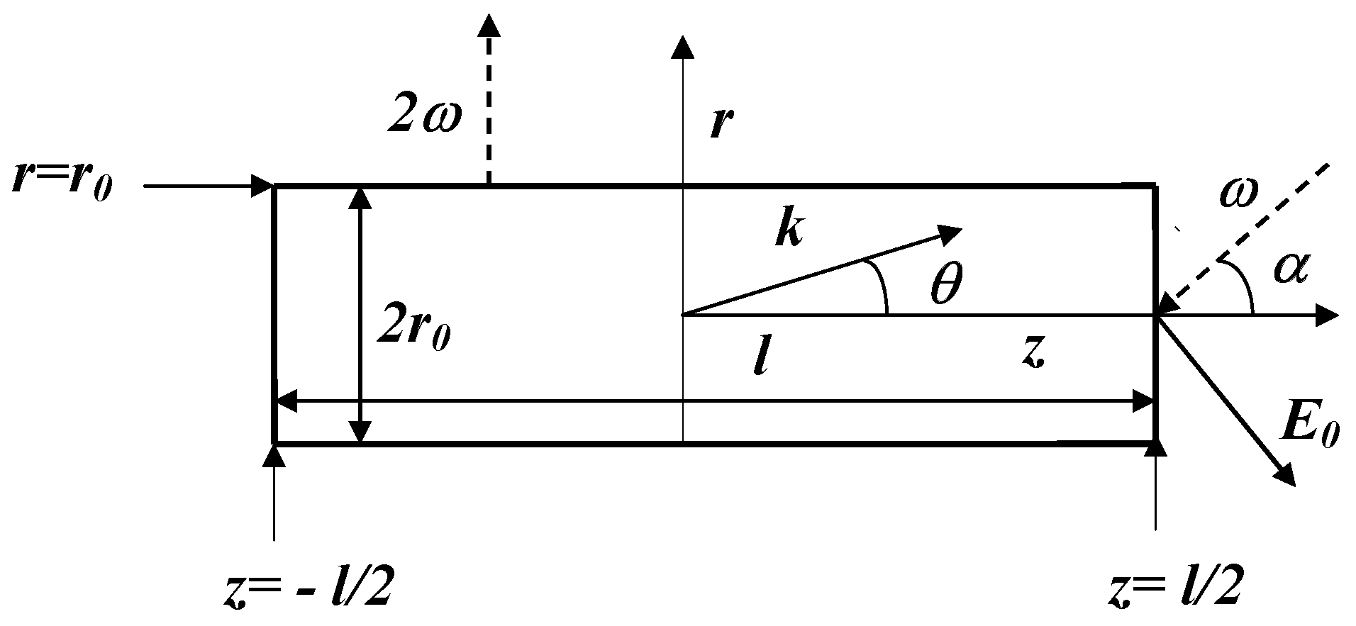
Though various geometrical shapes, such as silver-coated nanocones and bowtie antennas [6], gold nanospheres [7] and V-groove nanoparticle [8], have been discussed by other authors, we shall focus for simplicity upon the wire, sketched in Figure 1, containing conduction electrons of charge e, effective mass m and concentration and located in a cylindrical frame . It is assumed to sustain a wave, travelling along the z axis and conveying an electric field E, parallel to the z direction and taken to read
Figure 1.
Cross section of a cylindrical wire of length l and radius in the plane; the dashed lines labelled designate respectively the incoming electromagnetic wave of frequency , making an angle with the z direction, and the outgoing one of frequency , parallel to the radial axis; the solid lines labelled k, refer, respectively, to a one-electron wave-vector, making an angle with the z direction and the electric field carried along by the incoming wave.
To that end, let us begin with writing the expression of the force exerted by p upon a cylinder of axis z, length , section , containing thence of electrons
Then
showing up in the right-hand side of Equation (1), is identified as the force exerted on a single electron. The expression of will be worked out now by resorting to usual thermodynamical definitions [16,17], while assuming a unique temperature T all over the wire
with referring to a small volume, containing of electrons , local Helmholz free energy per unit-volume, Fermi energy, known as the chemical potential of independent electrons and space-charge density , respectively. Thus the pressure gradient is realized to ensue from the finite space-charge density . Note also that the macroscopic pressure p is unrelated to the so called quantum pressure, considered by other authors [4,9,10].
Besides, the field E induces [12,16,18] a dielectric displacement D, parallel to the z direction
with referring to the vacuum permittivity. Noteworthy is that the polarisation term (n stands for the refractive index), originating from the filled bands and contributing to in the Ampère-Maxwell equation, is lacking in Equation (2), because the corresponding electrons contribute nothing to . Linearising further D by dropping in Equation (2) and Fourier transforming it with respect to t yields
The space-charge density is given by Gauss’ equation [18], reading in this unidimensional analysis as
At last substituting to in Equation (1) and Fourier transforming the resulting expression with respect to , while taking advantage of Equation (4), gives
Thus combining Equations (3,5) together is seen to make up a Cramer system in terms of the unknowns , to be solved as
with being the plasma frequency [12]. Those expressions of are seen to be quite different from the corresponding formulae, valid for an electromagnetic wave [12] which can be deduced from Equation (1), after deleting , as
The charge conservation law [18] can be recast, by taking advantage of Equation (4) while assuming , as
Comparing Equation (8) with the Ampère-Maxwell equation [12] enables one to realise that the space-charge wave conveys no magnetic field, unlike electromagnetic waves.
The current density in Equation (8) is defined as with referring to the drift[12,16] and diffusion[13,14,15] components, respectively, both flowing along the z axis. They read [13,14,15,16]
with being a diffusion coefficient [13,14,15]. Linearising by dropping in Equation (9) and Fourier transforming the resulting expression of with respect to t and that of with respect to z lead to
with standing for Drude’s conductivity [12,16] and B given by Equation (6). The expression of in Equation (10) is to be compared with that of a current , aroused by an electromagnetic wave and obeying thence Ohm’s law [12,16]
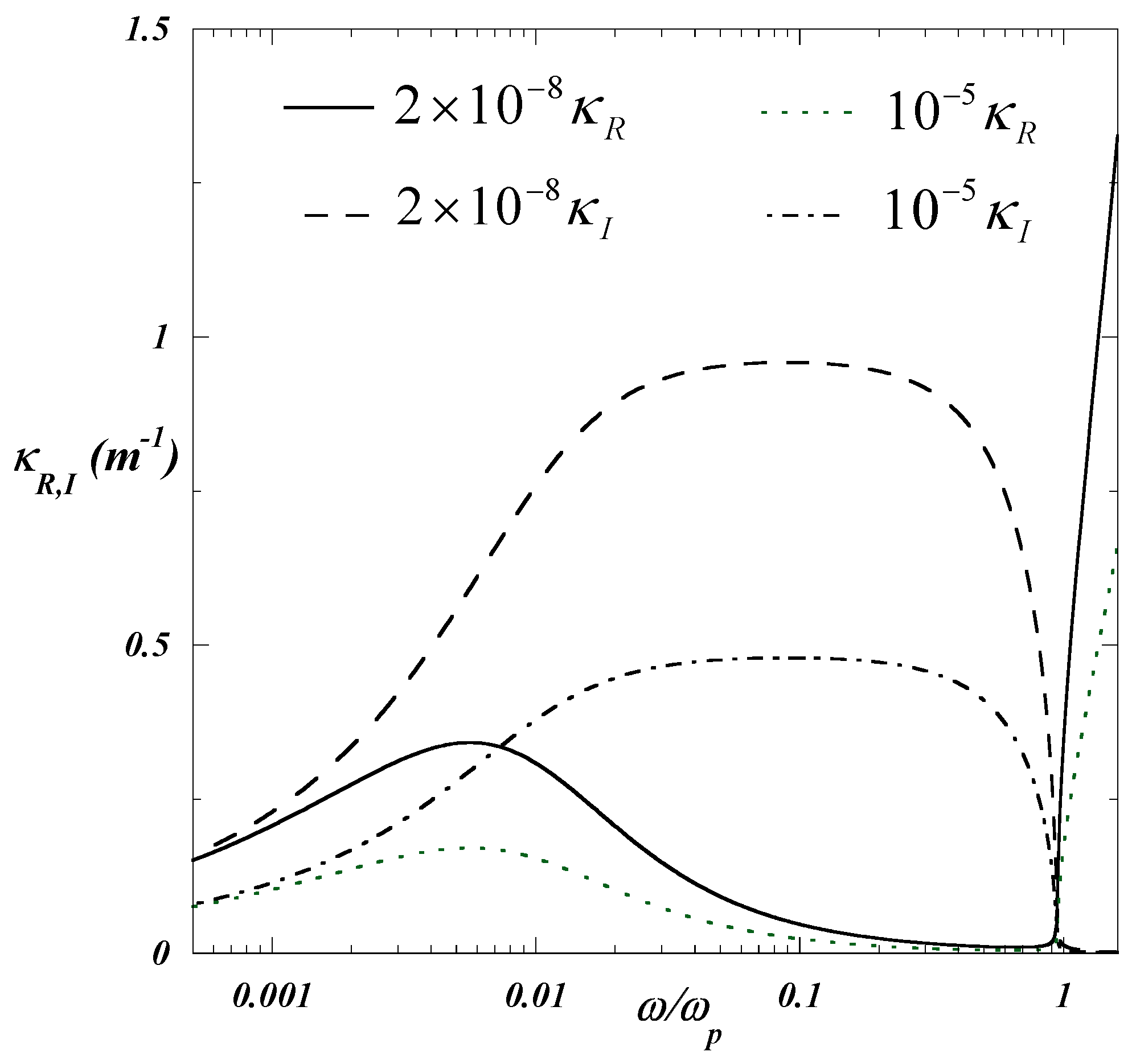
At last, Fourier transforming the charge conservation law in Equation (8) with respect to , while taking advantage of Equations (6,10), yields eventually the dispersion relation as
Explicit expressions are needed now for . To that end, the set of conduction electrons is assumed to make up an isotropic, 3-dimensional Fermi gas, either degenerate (metal) or not (semi-conductor). The one-electron energy and the corresponding density of states read in both cases
wherein and are defined in the caption of Figure 1. Moreover the origin of energy is taken at the bottom of the conduction band. Due to the electron velocity being equal to , each electron contributes to
with
being the Fermi-Dirac distribution [16], whereas refer, respectively, to Boltzmann’s constant and the mean free path, projected onto the z axis. Remarkably the conduction electrons are to be described below as a Fermi gas at local thermal equilibrium, characterised by a uniqueT, yet zdependent. The diffusion current density is then obtained by integrating over in reciprocal space
with being the radius of the spherical Brillouin zone and standing for the volume of the unit-cell, accommodating at most 2 electrons. Hence is inferred to be the upper bound of the conduction band. After integration with respect to , Equation (14) is recast into
Note that entails . The calculation of proceeds differently for a metal or a semi-conductor.
Since the T dependence of is negligible [16] in a metal up to room temperature, the calculation of will be made at , which yields
by assuming a half-filled band . Performing further the integration in Equation (15) owing to Sommerfeld’s expansion [16] gives eventually
By contrast, the conduction electron properties prove strongly T-dependent in semi-conductors [16], which implies near room temperature
for which designates the donor concentration. At last is inferred to read
3. 2-Matching Procedure
The electric field E can be now expressed as
with the unknowns to be assigned below. To that end, it ought to be noted that, since the longitudinal space-charge wave is to be aroused by an external transverse electromagnetic wave, the only practical way to couple both waves together consists of having the electromagnetic wave impinging upon the edge of the wire, as pictured in Figure 1. Thus requiring the projection of the dielectric displacement D onto the z axis to be continuous at implies
is given by Equation (6) and are respectively the light velocity, the amplitude of the electric component of the incoming wave, making an angle with the z axis (see Figure 1) and its projection onto the z axis, whereas is identified as the phase-shift of the incoming beam along the radial axis.
Actually allowing for would give rise to a superficial charge density
in accordance [18] with Equation (4). However, let us prove by contradiction that it cannot be so. Accordingly taking advantage [18] of and Equation (8) implies
Thence inserting the latter expression of into Equation (18) enables us to deduce , contradicting thereby our assumption . At last, by substituting the expressions of , as given in Equation (16), to in Equation (17), Equation (17) is turned into a Cramer system, the unknowns of which are found to read
4. 3-SHG
The polarisation and current density which have been discarded while linearising in Equations (2,9), are both realised to oscillate like and are thence recognised as the only source of SHG in this work. They read
which entails for their time-Fourier transforms owing to Equations (4,6)
The average values of over are needed to proceed further. They are inferred to read, thanks to Equations (16,19)
The SHG signal to be addressed now consists for in an electromagnetic wave of frequency propagating outward along the radial direction (see Figure 1) and carrying an electric component, parallel to the z axis
with the wave number . However for , induces in addition a drift current density , obeying Ohm’s law (see Equation (11)) and a dielectric displacement , both aligned with the z axis and reading [12]
with given by Equation (7). The complex number will be calculated now with help of the wave-equation [12]
The dispersion curve of electromagnetic waves
plotted in Figure 3, turns out to differ markedly from that of space-charge waves , pictured in Figure 2. Likewise, there is
for , whereas there is
for . Actually, the conditions and characterise, respectively, the surface plasmon-polaritons [11,12], for which the electromagnetic field is confined inside a narrow range in accordance with the skin effect [19], and three-dimensional plasmons, penetrating deeply into bulk matter due to . At last, it is worth noting that there is , as inferred from Equations (12,21) for , which entails that the associated space-charge and electromagnetic waves are identical in this particular case, since both are characterised by
but vanishing space-charge density and magnetic field. Besides, the plasma oscillation ought to take place at rather than , as arbitrarily purported in textbooks [12,16,20] to ensue from with defined in Equation (7).
The unknown will be assigned thanks to Equations (11,20), by substituting to , respectively, in the wave-equation (21), which yields finally
with given by Equation (7).
The incoming electromagnetic power and the outgoing one can thence be inferred to read
The property
is a signature of the non-linear character of SHG [1]. Moreover reaches its upper bound for deg.
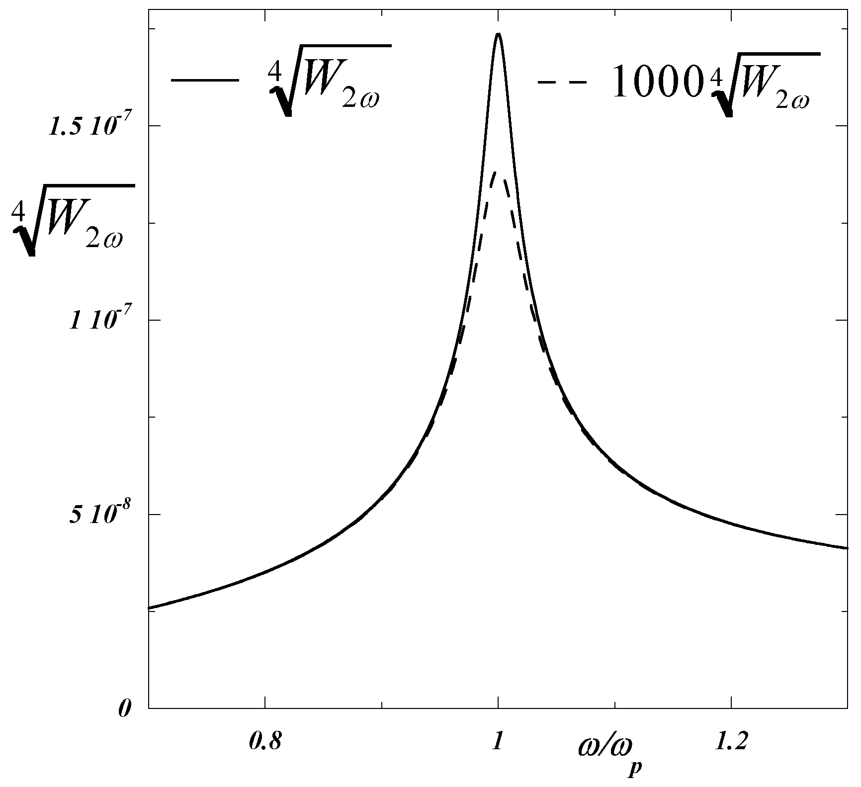
The outgoing power has been plotted in Figure 4 for a metal and a semi-conductor. Both plots exhibit a sharp maximum at , ensuing from with , as inferred from Equation (6) for . decreases to 0 with , whereas it reaches a plateau for . The huge ratio (semi-conductor)(metal), conspicuous in Figure 4, stems from
Such a behaviour, ensuing from
in Equations (20,22), respectively, is thence realised to concur with the ratio of -values, assumed in Figs.2,4. Therefore choosing a semi-conducting sample of short length l is likely to greatly enhance the SHG efficiency. Besides, semi-conductors exhibit two additional merits :
- semi-conductors, unlike metals of fixed , enable one to tune to the searched frequency, either by controlling the doping rate or monitoring the temperature;
- the relatively low value of rad/s, typical of donor-like semi-conductors permits to benefit from a broader frequency range above rad/s than in metals and acceptor-like semi-conductors, for which this threshold is pushed up above rad/s. Moreover this analysis breaks down in the microscopic limit for , which, in view of Equation (12), sets upper limits rad/s and rad/s for metals and semi-conductors, respectively.
Figure 4.
Plot of the SHG power at frequency , expressed in with V/m, nm, nm; the solid and dashed lines depict the data reckoned for a semi-conductor and a metal, respectively; the various parameters, used for the calculations, have been assigned to the same values, as already taken for Figure 2.
Figure 4.
Plot of the SHG power at frequency , expressed in with V/m, nm, nm; the solid and dashed lines depict the data reckoned for a semi-conductor and a metal, respectively; the various parameters, used for the calculations, have been assigned to the same values, as already taken for Figure 2.
5. Conclusions
The properties of longitudinal space-charge waves have been worked out with help of Equations (1,4,8) and strong emphasis has been put on their being quite different from transverse electromagnetic waves which are rather solutions of Maxwell’s equations [12,18]. Accordingly, a space-charge wave carries no magnetic field, whereas an electromagnetic wave carries no three-dimensional space-charge, even though the electromagnetic field may be strongly spatially inhomogeneous [9,10,11]. However most of textbooks [12,20] purport wrongly that the same dielectric displacement D comes up, on the one hand, in the Ampère-Maxwell equation and on the other hand, in Gauss’ equation (see Equation (4)) and the charge conservation law (see Equation (8)). Unfortunately such a claim is inconsistent in two respects :
- as already recalled above, D contains only the polarisation, stemming from the conduction electrons in Gauss’ equation and the charge conservation law, whereas D includes in addition that of filled bands in the Ampère-Maxwell equation;
- there is for Gauss’ equation and the charge conservation law versus for the Ampère-Maxwell equation.
Hopefully this work will help dispel this ubiquitous and harmful confusion.
Figure 1 illustrates how matching both waves together might provide with a novel mechanism of SHG, instrumental over a wide frequency range in semi-conductors. Light has been shed on the advantage offered by nanometric samples. The concentration dependence of turns out to be redolent of a similar behaviour of the Hall voltage, varying [21] like . Note also that the -dimensional space charge discussed here, is quite different from the -dimensional superficial charge density, conveyed by a surface plasmon polariton [11,12]. Last but not least, the dependences of , unveiled here, lend themselves to an experimental check.
Acknowledgments
One of us (J.S.) is beholden to Eric Bringuier, Carsten Henkel and the Referee for helpful criticisms.
References
- J. Szeftel et al., Opt.Comm., 305, 107 (2013).
- N. Simon and N. Bloembergen, Phys.Rev., 171, 1104 (1968).
- N. Bloembergen et al., Phys.Rev., 174, 813 (1968).
- N. Sipe et al., Phys.Rev.B, 21, 4389 (1980).
- Chaojin Zhang, Chengpu Liu and Zhizhan Xu, Phys.Rev A, 88, 035805 (2013).
- A. Husakou, S.-J. Im and J. Herrmann, Phys.Rev A, 83, 043839 (2011).
- A. Slablab et al., Opt.Expr., 20, 220 (2012).
- A. Hille et al., J.Phys.Chem.C, 120, 1163 (2016).
- Henglei Du and Chengpu Liu, IEEE, 72, 2592 (2024).
- Henglei Du, Wenkang Wang and Chengpu Liu, Micro and Nanostructures, 188, 207784 (2024).
- Rafi Ud Din, Hazrat Ali and Rashid Ahmad, Phys.Lett. A, 532, 130202 (2025).
- S.A. Maier, Plasmonics, Fundamental and Applications, Springer (2007).
- B.K. Ridley, Quantum Processes in Semiconductors, Clarendon Oxford (1999).
- J. Szeftel et al., Europhys.Lett., 73, 752 (2006).
- J. Szeftel and G.X. Huang, Inter.J.Mod.Phys.B, 21, 4201 (2007).
- N.W. Ashcroft and N. D. Mermin, Solid State Physics, Saunders College (1976).
- L.D. Landau and E.M. Lifshitz, Statistical Physics, ed. Pergamon Press, London (1959).
- J.D. Jackson, Classical Electrodynamics, John Wiley & Sons, New York (1999).
- J. Szeftel et al., Phys.Lett.A, 381, 1525 (2017).
- M.P. Marder, Condensed Matter Physics, John Wiley & Sons, New York (2000).
- J. Szeftel and J.C.S. Lévy, Euro.Phys.J.WOC, 300, 01009 (2024).
Figure 2.
Plot of as given by Equation (12), calculated with nm, K and ; the solid and dashed lines refer to the data reckoned for a metal with electron per unit-cell, rad/s, J×m3, m2s, whereas the dotted and dashed-dotted lines depict the data, obtained for a semi-conductor with electron per unit-cell, rad/s, J×m3, m2s.
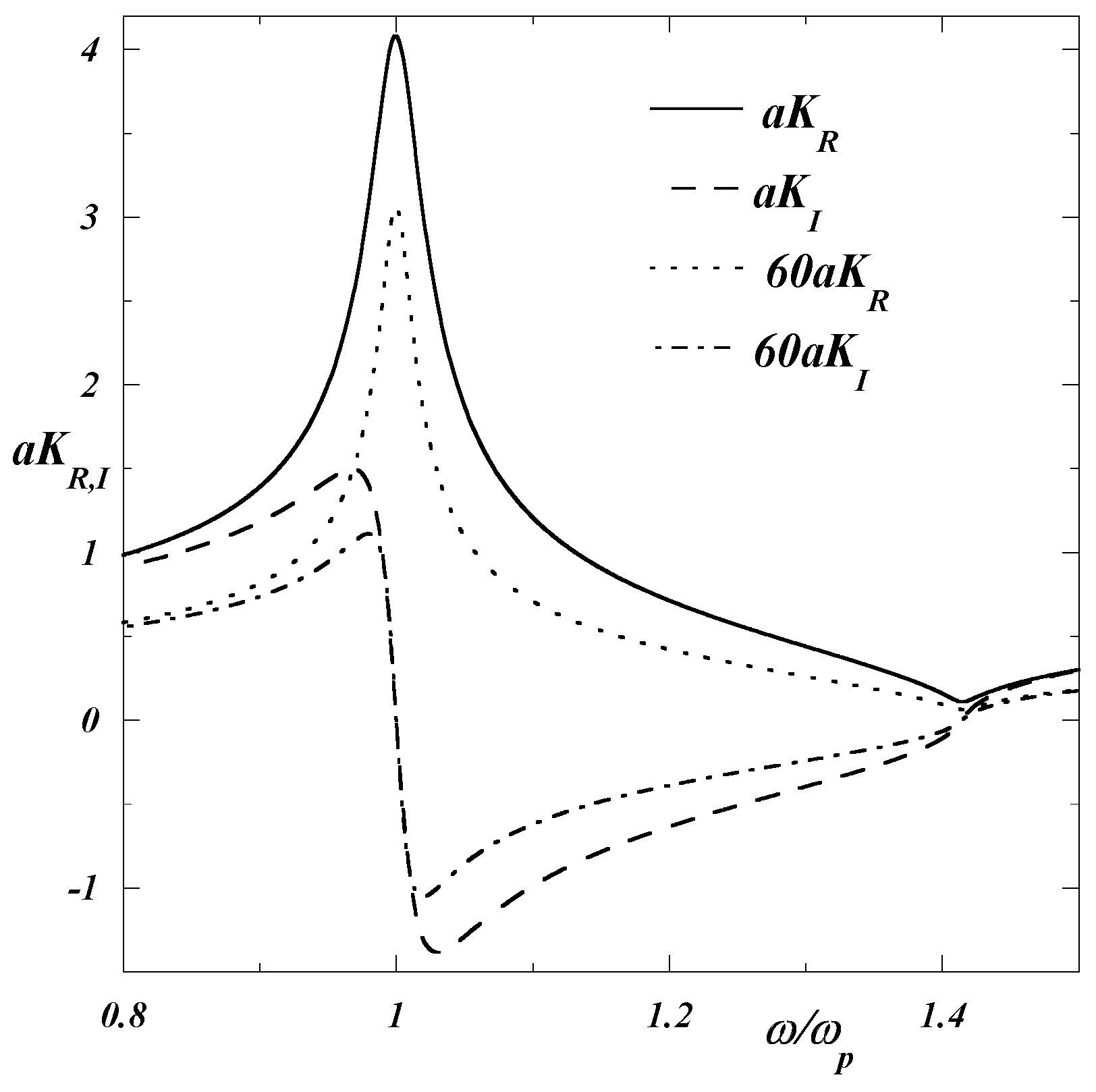
Figure 3.
Plot of as given by Equation (21), calculated with and ; the solid and dashed lines refer to the data reckoned for a metal with rad/s, whereas the dotted and dashed-dotted lines depict the data, obtained for a semi-conductor with rad/s.
Figure 3.
Plot of as given by Equation (21), calculated with and ; the solid and dashed lines refer to the data reckoned for a metal with rad/s, whereas the dotted and dashed-dotted lines depict the data, obtained for a semi-conductor with rad/s.
Disclaimer/Publisher’s Note: The statements, opinions and data contained in all publications are solely those of the individual author(s) and contributor(s) and not of MDPI and/or the editor(s). MDPI and/or the editor(s) disclaim responsibility for any injury to people or property resulting from any ideas, methods, instructions or products referred to in the content. |
© 2025 by the authors. Licensee MDPI, Basel, Switzerland. This article is an open access article distributed under the terms and conditions of the Creative Commons Attribution (CC BY) license (http://creativecommons.org/licenses/by/4.0/).
Copyright: This open access article is published under a Creative Commons CC BY 4.0 license, which permit the free download, distribution, and reuse, provided that the author and preprint are cited in any reuse.


