Submitted:
17 February 2025
Posted:
18 February 2025
You are already at the latest version
Abstract
Microring resonators have become one of the key components for realizing signal processing, generation, and integration in microwave photonics, owing to their high Q factor, compact footprint, and tunability. However, most of the reported microring resonators are confined to the single-mode regime. In this paper, we design an ultra-compact multimode microring resonator (MMRR) based on shape-optimized multimode waveguide bends (MWBs). Cubic spline curves are used to represent the MWB boundary and the adjoint methods are utilized for inverse optimization, achieving an effective radius of 8 μm. Asymmetric directional couplers (ADCs) are designed to independently couple three modes into multimode microring, according to phase-matching conditions and transmission analysis. The MMRR is successfully fabricated on a commercial platform using 193-nm dry lithography process. The device exhibits high loaded Q factors of 2.3 × 10⁵, 4.1 × 10⁴ and 2.9 × 10⁴, and large free spectral ranges (FSRs) of 5.4, 4.7 and 4.2 nm for TE0, TE1 and TE2 modes, with about 19 × 55 μm² footprint.
Keywords:
microring resonator
; inverse design
; multimode waveguide bend
; silicon photonics
; microwave photonics
1. Introduction
Currently, communication systems face significant challenges in terms of energy consumption and bandwidth, and microwave photonics is an important technological solution to address these challenges [1]. However, traditional microwave photonic systems still suffer from large size, poor stability, and high power consumption. The application of photonic integration technology can not only greatly reduce the system size and power consumption but also significantly enhance its performance, holding the promise of realizing a single microwave photonics processing chip [2]. Microring resonators, one of the key components in integrated optics, have demonstrated excellent performance in high speed modulators [3,4], optical switches [5,6], microwave photonic filters [7,8] and many other fields. Meanwhile, to enhance the communication capacity of optical networks, the utilization of multiplexing technology has emerged as an effective strategy. Combined with silicon-based optoelectronics technology, a variety of chip-scale multiplexing devices and systems have been reported [9,10,11]. Mode division multiplexing (MDM) devices enable simultaneous parallel data transfers on a single physical channel, having been attracted widespread attention [12,13]. Recently, numerous multimode devices have been demonstrated for silicon-based MDM systems, including mode (de)multiplexers [14,15], multimode waveguide crossings [16,17], multimode power splitters [18,19] and multimode fiber-to-chip couplers [20,21].
However, most of the microring resonators are designed to operate in the fundamental mode case, limited by mode crosstalk and mode dispersion. Separately optimizing microring resonator parameters for each mode is clearly effective for multimode multiplexing [22,23], however multiple microrings will increase the overall size of the device. Several schemes to realize a multimode MMRR have been reported. In [24], a shape-optimized MWB based on transformation optics is demonstrated and applied into a MMRR, whereas the effective radius of the MWB is 15 μm. In [25], a MMRR composed of modified Euler waveguide bends and subwavelength grating (SWG) coupler is designed, but the MMRR exhibits high insertion loss (IL) and mode crosstalk. Meanwhile, small feature sizes of the SWG coupler may not be compatible with standard silicon photonics fabrication processes. Another novel MMRR is proposed and demonstrated in [26], with the help of total internal reflection (TIR) effect. However, the insertion loss of this MMRR is also large due to the scattering at the TIR mirror surface.
In this work, we propose and demonstrate an ultra-compact and low-loss MMRR on a commercial 220-nm silicon-on-insulator (SOI) platform. The MMRR consists of optimized MWBs and multimode straight waveguides, supporting the first three-order modes (, and ). The shape of the MWB is described by cubic spline curves and is inverse designed and optimized by adjoint methods. The proposed MWB which is also used as a bending directional coupler for mode, possesses an effective radius of 8 μm. The and modes are coupled into MMRR through corresponding ADC, and the total length of MMRR is about 123 μm. The fabricated MMRR exhibits > loaded Q factors and about 5 nm FSR for the three modes.
2. Design and Simulation
2.1. The Design of Multimode Waveguide Bend (MWB)
Conventional MWB usually require a very large bending radius to avoid undesired losses and inter-mode crosstalk due to mode mismatch [24,27]. The performance of MWB is strongly dependent on its shape, and several different special mathematical curves have been employed to optimize the MWB [28,29,30,31]. Among them, the cubic spline interpolation curves possess a high degree of freedom and not limited by the well-defined curve functions [31]. For a given set of n data points (, ) that follow, a smooth curve can be obtained by cubic spline interpolation, in which the adjacent data points are fitted by a cubic polynomial,
where i = 1, 2, …, n-1, is the ith spline curve, , and are unknown coefficients. Cubic spline curves require the segments to be continuous at the nodes, and the first-order and second-order derivatives to be continuous at the nodes, which can be expressed as follows:
It can be seen that the total number of unknown coefficients is 3n-3 from (1), while only 3n−5 equations can be formulated according to (2). Thus, it is often necessary to impose additional boundary conditions at the start and end points of the spline curve in practical applications. A commonly employed natural boundary condition can be formulated as follows [31]:
By combining (1) to (3), we can solve for all the undetermined coefficients.
As shown in Figure 1a, in order to balance the trade-off between device size and performance, we choose the effective radius of the MWB as 8 μm. The width of both ends of the MWB is 1.3 μm, consistent with the straight multimode waveguide, supporting the first three-order TE modes. The MWB consists of two identical 45-degree curved sections, with its boundary outlined by two sets of cubic spline interpolation points, which are marked as blue circles. To obtain accurate device performance and smooth curve shapes, we choose 20 and 15 interpolation points in the inner and outer curves of the MWB. The optimization of this MWB by using traditional parameter scanning methods requires a large amount of computational resources and time. Therefore, we employ the adjoint method to optimize the dataset, which is significantly efficient for the inverse design of complex electromagnetic components [32,33]. By calculating the gradient of figure-of-merit (FOM) through only two simulations in each iteration, namely forward and adjoint simulations, the adjoint method can significantly accelerate the optimization process .
The FOM is defined as mode overlap (η) between input mode and the corresponding output mode of the MWB, similar to formulations in [27,34], which is easy to implement in Lumerical. The total FOM can be written as:
where i denotes the ith mode. A 1/4 ring waveguide with a radius of 8 μm and a width of 1.3 μm is chosen as the initial structure, and the interpolation points are uniformly distributed. Aided by the shape optimization within the Lumopt module of Ansys Lumerical, the 3D finite-difference time-domain (FDTD) solver is selected to maximize the FOM, and the L-BFGS-B algorithm is used to update the parameters [35,36]. The structure of the optimized MWB approximates a 1/4 circle that is wider at both ends and narrower in the middle. Figure 2 illustrates the optical field distributions of three modes through the MWB and the corresponding insertion loss and crosstalk curves. It can be seen that no significant mode mismatch between input and output waveguide ports. Moreover, within the wavelength range of 1.5 to 1.6 μm, the average losses for the , and modes are 0.01 dB, 0.03 dB, and 0.03 dB, and the crosstalk are below -21.3 dB, -17.9 dB, and -17.3 dB, respectively.
2.1. The Design of Multimode Microring Resonator (MMRR)
The proposed MMRR consists of a multimode microring located at the center and three ADCs positioned at the periphery, as shown in Figure 1b. According to the coupled mode theory [37], when two waveguides are close enough, there will be periodic energy exchange between them via the evanescent fields. The employed ADC consists of a single-mode waveguide and a multimode waveguide, which enables mode conversion between a fundamental mode and a high-order mode. To achieve efficient mode conversions, the three coupling regions should be designed carefully, including widths of access waveguides, coupling lengths and gaps between waveguides, as shown in Figure 3.
Figure 4a shows the effective indices of first three-order modes in the waveguides with different widths at the wavelength of 1.55 μm, calculated by finite difference eigenmode method. For the and modes, should be fulfilled according to the phase-matching condition, where is the effective indices for the modes of two access waveguides and is the effective indices for the or modes of multimode waveguide. Based on this principle, we choose the widths of the access waveguides ( and ) as 0.64 μm and 0.41 μm, respectively. Moreover, A bending ADC is used to couple the mode of narrow access waveguide into the mode of MWB. Similarly, should be fulfilled according to the phase-matching condition [38], where and are radii of curvature of the two bending waveguides. The width of the ADC can be calculated as 0.52 μm according to this formula.
Coupling lengths and gaps between waveguides affect the coupling coefficients of the MMRR, which determine the MMRR performance like IL and extinction ratio (ER). To make the MMRR suitable for integrated optoelectronic applications, a large FSR and ER are usually required. Thus, the expected FSR and ER of the MMRR are set to 5 nm and 20 dB. The FSR of an all-pass microring resonator can be expressed as below:
where = 1.55 μm, is the group refractive index of the mode and L is the circumference of the multimode microring. is defined as follows:
Figure 4b demonstrates the effective refractive index of each mode as a function of wavelength. We fit it to a straight line using the least-squares method and derive the slope of the line to be brought into (6) to obtain of each mode. We first consider the mode in the multimode waveguide, which has a of 3.9 at wavelength of 1.55 μm, so circumference L can be derived from (5) as 123.18 μm under the target of an FSR of 5 nm.
To choose the coupling coefficients t of the three ADCs, we consider the relationship between the self-coupling coefficient and ER in the all-pass microring resonator, which can be expressed as follows [39]:
where α is the attenuation factor of multimode microring. For ring SOI waveguide with 5 - 10 μm bending radius, the loss is generally considered to be 5-20 dB/cm, which corresponds to an attenuation factor α of 0.98-0.99. Considering the inevitable fabrication errors, we analyzed three representative values of α, namely 0.98, 0.985 and 0.99, by which t can be calculated according to (7).
Once coupling coefficients t is clear, we can choose the appropriate coupling length by 3D FDTD simulations. To reduce the complexity of device fabrication while simultaneously maintaining a compact device size, we selected the gaps of the three ADCs to be 200 nm, 200 nm, and 300 nm, respectively. Taking the case of α = 0.985 as an example, by doing 3D FDTD parameter scanning, we can derive the corresponding coupling region angle and lengths of the three ADCs as 51.4 degrees, 10.57 μm and 2.3 μm at the wavelength of 1.55 μm. Figure 5 illustrates the optical field distributions for launched , and modes in the three ADCs. In the ADC, the performance of the bending coupling is guaranteed due to the refractive index matching between the modes and the fact that the interpolation points at the outer boundary of the MWB are almost distributed along a conventional 1/4 bend. In the other two ADCs, the and modes injected from the bus multimode waveguide are coupled to the corresponding modes of the access waveguides as expected. No mode crosstalk is observed in each ADC.
Some of design parameters for three ADCs of the MMRR are listed in Table 1, in which α is a dimensionless parameter. In addition, other parameters can be summarized as follows: = 0.52 μm, = 0.64 μm, = 0.41 μm, = 1.3 μm, = 0.2 μm, = 0.2 μm, = 0.3 μm.
We also calculated the coupling coefficient t at different wavelengths using 3D FDTD solver, when the above parameters are employed. As illustrated in Figure 6, in wavelength range of 1.5 to 1.6 μm, t is higher than 0.97 and increases with α. Since the coupling coefficient t is no longer linearly related to the wavelength, we can use polynomial fitting to derive the corresponding mathematical expression.
The transmission spectrums of the three modes in the MMRR are then calculated. The relationship between transmission efficiency (T) and the wavelength of an all-pass microring can be expressed as follows [39]:
where , which is the phase of the optical wave after propagating one complete round trip in the microring. Simultaneously considering the dispersion characteristics of and t shown in the Figure 4b and Figure 6, theoretical transmission spectrum for each mode can be calculated according to (8).
As shown in Figure 7, under these different α, the FSRs of the three modes are 5.2 nm, 5 nm and 5.9 nm, respectively. Here we need to point out that, since we firstly determine the circumference of the multimode microring based on the of the mode with (5), and this value will not be changed for a determined MMRR, which leads to a slight difference in the FSR due to the distinction of the three modes.
3. Fabrication and Characterization
Using a 193-nm dry lithography process, the designed MMRR are fabricated on a 220nm-thick SOI wafer with a 3-μm-thick silicon dioxide buried layer at Advanced Micro Foundry, Singapore. Figure 8 presents the microscope image of the devices, with clear boundaries and smooth contours shown in the etched MMRR. The footprint of the MMRR is only ∼19 × 55 μm2, and six identical grating couplers are used for optical transmission between the device and single-mode fibers.
An amplified spontaneous emission source and an optical spectrum analyzer are used to measure the transmission spectrums of each mode in the fabricated MMRR. The transmission spectrum of the reference waveguide without the presence of the multimode microring is measured firstly for normalization. The real transmission spectrums of each mode in MMRR are then obtained by subtracting the reference one, as shown in Figure 9 (a) – (c). Here, the spectrums are only show in a 20 nm range for better observation of FSRs. All three modes in the MMRR exhibit ILs below -1dB in the measured wavelength range. Besides, the transmission spectrums of each mode contain only one set of uniformly distributed resonance peaks, suggesting that crosstalk between modes is negligible.
We select the resonant peaks near 1546.18 nm, 1548.55 nm and 1547.67 nm for the three modes to analyze the loaded Q factors of the MMRR, and utilize Lorentzian curves to fit the measured data, as shown in Figure 9 (d) – (f). The full widths at half-maximum are 6.3 pm, 37.1 pm and 54.3 pm for , and modes, corresponding to calculated loaded Q factors of , and , respectively. Moreover, the FSRs for and modes are 5.1 nm and 4.7 nm, which are close to the calculated values. The FSR for mode is 4.2 nm, with a larger difference to the calculated value. This may come from that the coupling length of ADC is the smallest, so it is most susceptible to process errors. Nonetheless, the fabricated MMRR still exhibits a sufficiently large FSR in all three modes, which is highly advantageous for the applications like wavelength division multiplexing, optical sensing and microwave photonics.
4. Conclusions
In summary, we propose and experimentally demonstrate a compact MMRR on a commercial 220-nm SOI platform, which is composed of shape-optimized MWBs and ADCs. Two cubic spline curves are chosen to define the MWB and the adjoint methods are used for optimization, achieving an effective radius of 8 μm. Three ADCs are carefully designed according to the phase-matching condition and desired transmission performance. The fabricated MMRR exhibits high loaded Q factors of to , and large FSRs of 4.2 to 5.1 nm for , and modes. The device footprint is only ∼19 × 55 μm², making it highly suitable for integrated optoelectronic applications. This work demonstrates the potential of ultra-compact MMRR for high-density integration in next-generation optical communication systems and microwave photonics.
Author Contributions
Conceptualization, Z.L. and C.C.; methodology, Z.L. and C.C.; software, C.C.; validation, Z.L. and C.C.; formal analysis, C.C.; investigation, Z.L.; resources, Z.L.; data curation, C.C.; writing—original draft preparation, Z.L.; writing—review and editing, Z.L. and C.C.; visualization, Z.L. and C.C.; supervision, L.Y.; project administration, X.F. and L.Y.; funding acquisition, X.F. and L.Y. All authors have read and agreed to the published version of the manuscript.
Funding
This research received no external funding.
Institutional Review Board Statement
Not applicable.
Informed Consent Statement
Not applicable.
Data Availability Statement
Relevant data are available from the authors upon reasonable request.
Conflicts of Interest
The authors declare no conflicts of interest.
Abbreviations
The following abbreviations are used in this manuscript:
| MMRR | multimode microring resonator |
| MWB | multimode waveguide bend |
| ADC | asymmetric directional coupler |
| FSR | free spectral range |
| MDM | mode division multiplexing |
| SWG | subwavelength grating |
| IL | insertion loss |
| TIR | total internal reflection |
| SOI | silicon-on-insulator |
| FOM | figure-of-merit |
| FDTD | finite-difference time-domain |
| ER | extinction ratio |
References
- Yao, J.; Capmany, J. Microwave Photonics. Sci. China Inf. Sci. 2022, 65, 221401. [Google Scholar] [CrossRef]
- Marpaung, D.; Yao, J.; Capmany, J. Integrated Microwave Photonics. Nature Photon 2019, 13, 80–90. [Google Scholar] [CrossRef]
- Zhang, Y.; Zhang, H.; Zhang, J.; Liu, J.; Wang, L.; Chen, D.; Chi, N.; Xiao, X.; Yu, S. 240 Gb/s Optical Transmission Based on an Ultrafast Silicon Microring Modulator. Photon. Res. 2022, 10, 1127. [Google Scholar] [CrossRef]
- Yuan, Y.; Peng, Y.; Sorin, W.V.; Cheung, S.; Huang, Z.; Liang, D.; Fiorentino, M.; Beausoleil, R.G. A 5 × 200 Gbps Microring Modulator Silicon Chip Empowered by Two-Segment Z-Shape Junctions. Nat Commun 2024, 15, 918. [Google Scholar] [CrossRef] [PubMed]
- Jia, H.; Zhao, Y.; Zhang, L.; Chen, Q.; Ding, J.; Fu, X.; Yang, L. 5-Port Optical Router Based on Si Microring Optical Switches for Photonic Networks-on-Chip. IEEE Photon. Technol. Lett. 2016, 1–1. [Google Scholar] [CrossRef]
- Liu, S.; Huo, Y.; Cheng, C.; Niu, J.; Fu, X.; Yang, L. Ultra-Compact On-Chip Silicon Photonic Polarization- and Wavelength-Selective Switch. Journal of Lightwave Technology 2024, 42, 8793–8801. [Google Scholar] [CrossRef]
- Tao, Z.; Tao, Y.; Jin, M.; Qin, J.; Chen, R.; Shen, B.; Wu, Y.; Shu, H.; Yu, S.; Wang, X. Highly Reconfigurable Silicon Integrated Microwave Photonic Filter towards Next-Generation Wireless Communication. Photon. Res. 2023, 11, 682. [Google Scholar] [CrossRef]
- Yan, H.; Xie, Y.; Zhang, L.; Dai, D. Wideband-Tunable on-Chip Microwave Photonic Filter with Ultrahigh- Q U-Bend-Mach–Zehnder-Interferometer-Coupled Microring Resonators. Laser & Photonics Reviews 2023, 2300347. [Google Scholar] [CrossRef]
- Zhao, W.; Peng, Y.; Cao, X.; Zhao, S.; Liu, R.; Wei, Y.; Liu, D.; Yi, X.; Han, S.; Wan, Y.; et al. 96-Channel on-Chip Reconfigurable Optical Add-Drop Multiplexer for Multidimensional Multiplexing Systems. Nanophotonics 2022, 11, 4299–4313. [Google Scholar] [CrossRef]
- James, A.; Novick, A.; Rizzo, A.; Parsons, R.; Jang, K.; Hattink, M.; Bergman, K. Scaling Comb-Driven Resonator-Based DWDM Silicon Photonic Links to Multi-Tb/s in the Multi-FSR Regime. Optica 2023, 10, 832. [Google Scholar] [CrossRef]
- Yi, X.; Zhao, W.; Li, C.; Zhang, L.; Xiang, Y.; Liu, C.; Shi, Y.; Liu, L.; Dai, D. Reconfigurable Optical Add-Drop Multiplexers for Hybrid Mode-/Wavelength-Division-Multiplexing Systems. Adv. Photon. Nexus 2023, 2. [Google Scholar] [CrossRef]
- Mojaver, K.R.; Safaee, S.M.R.; Morrison, S.S.; Liboiron-Ladouceur, O. Recent Advancements in Mode Division Multiplexing for Communication and Computation in Silicon Photonics. Journal of Lightwave Technology 2024, 42, 7860–7870. [Google Scholar] [CrossRef]
- Li, C.; Liu, D.; Dai, D. Multimode Silicon Photonics. Nanophotonics 2019, 8, 227–247. [Google Scholar] [CrossRef]
- Wu, X.; Huang, C.; Xu, K.; Shu, C.; Tsang, H.K. Mode-Division Multiplexing for Silicon Photonic Network-on-Chip. J. Lightwave Technol. 2017, 35, 3223–3228. [Google Scholar] [CrossRef]
- Dai, D.; Li, C.; Wang, S.; Wu, H.; Shi, Y.; Wu, Z.; Gao, S.; Dai, T.; Yu, H.; Tsang, H. 10-Channel Mode (de)Multiplexer with Dual Polarizations. Laser & Photonics Reviews 2018, 12, 1700109. [Google Scholar] [CrossRef]
- Zhao, W.; Yi, X.; Peng, Y.; Zhang, L.; Chen, H.; Dai, D. Silicon Multimode Waveguide Crossing Based on Anisotropic Subwavelength Gratings. Laser & Photonics Reviews 2022, 16, 2100623. [Google Scholar] [CrossRef]
- Chang, W.; Zhang, M. Silicon-Based Multimode Waveguide Crossings. J. Phys. Photonics 2020, 2, 022002. [Google Scholar] [CrossRef]
- Liu, R.; Lu, L.; Zhang, P.; Chang, W.; Liu, D.; Zhang, M. Integrated Dual-Mode 3-dB Power Splitter Based on Multimode Interference Coupler. IEEE Photon. Technol. Lett. 2020, 32, 883–886. [Google Scholar] [CrossRef]
- Fu, X.; Yang, S.; Niu, J.; Zhang, G.; Jia, H.; Yang, L. Carrier Depletion High-Speed Tunable Dual-Mode Converter for Mode-Division Multiplexing Networks. IEEE Photon. Technol. Lett. 2022, 34, 1242–1245. [Google Scholar] [CrossRef]
- Sun, S.; Fu, Y.; Li, S.; Ning, X.; Zhou, Z.; Zhang, D.; Wang, X. Ultra-Broadband Multimode Fiber-to-Chip Edge Coupler Based on Periodically Segmented Waveguides. Opt. Lett. 2024, 49, 6061. [Google Scholar] [CrossRef]
- Zhang, R.; Li, X.; He, Y.; Chen, G.; Xiong, L.; Chen, H.; Fontaine, N.K.; Zhang, Y.; Xie, W.; Su, Y. Ultra-High Bandwidth Density and Power Efficiency Chip-To-Chip Multimode Transmission through a Rectangular Core Few-Mode Fiber. Laser & Photonics Reviews 2023, 2200750. [Google Scholar] [CrossRef]
- Tan, J.; Xiao, H.; Ma, M.; Zhou, X.; Yuan, M.; Dubey, A.; Boes, A.; Nguyen, T.G.; Ren, G.; Su, Y.; et al. Arbitrary Access to Optical Carriers in Silicon Photonic Mode/Wavelength Hybrid Division Multiplexing Circuits. Opt. Lett. 2022, 47, 3531. [Google Scholar] [CrossRef]
- Jia, H.; Fu, X.; Zhou, T.; Zhang, L.; Yang, S.; Yang, L. Mode-Selective Modulation by Silicon Microring Resonators and Mode Multiplexers for on-Chip Optical Interconnect. Opt. Express 2019, 27, 2915. [Google Scholar] [CrossRef]
- Cai, L.; Gao, D.; Dong, J.; Hou, J.; Yang, C.; Chen, S.; Zhang, X. Compact and High Q-Factor Multimode Racetrack Ring Resonator Based on Transformation Optics. Opt. Express 2022, 30, 15766. [Google Scholar] [CrossRef]
- Chen, Z.; Ye, M.; Zhang, L.; Zhang, Q. Compact Mode-Insensitive Ring Resonator Based on SWG Coupler and Euler Bends. In Proceedings of the AOPC 2021: Micro-optics and MOEMS; SPIE, November 24 2021; Vol. 12066; pp. 144–149. [Google Scholar]
- Ye, M.; Sun, C.; Yu, Y.; Ding, Y.; Zhang, X. Silicon Integrated Multi-Mode Ring Resonator. Nanophotonics 2021, 10, 1265–1272. [Google Scholar] [CrossRef]
- Yang, S.; Jia, H.; Niu, J.; Fu, X.; Yang, L. CMOS-Compatible Ultra-Compact Silicon Multimode Waveguide Bend Based on Inverse Design Method. Optics Communications 2022, 523, 128733. [Google Scholar] [CrossRef]
- Dou, T.; Yue, S.; Hou, Y.; Wang, R.; Shi, H.; Li, Y.; Feng, Y.; Zhang, Z. Ultra-Sharp Multimode Waveguide Bends Based on Superellipse Curves and Shallowly Etched Nanoslots Designed by an Intelligent Algorithm. J. Light. Technol. 2024, 42, 5249–5261. [Google Scholar] [CrossRef]
- Li, W.; Chen, J.; Zhu, M.; Dai, D.; Shi, Y. Ultra-Compact Multimode Waveguide Bend With Optimized Dual Bezier Contours. IEEE Photon. Technol. Lett. 2023, 35, 1131–1134. [Google Scholar] [CrossRef]
- Liao, J.; Tian, Y.; Yang, Z.; Xu, H.; Dai, T.; Zhang, X.; Kang, Z. Broadband and Compact Silicon Multimode Waveguide Bends Based on Hybrid Shape Optimization. Journal of Lightwave Technology 2024, 42, 4882–4891. [Google Scholar] [CrossRef]
- Zhang, E.; Yang, S.; Zhang, L. General Waveguide Bend Design Based on Cubic Spline Interpolation and Inverse Design. J. Light. Technol. 2024, 42, 4614–4625. [Google Scholar] [CrossRef]
- Lalau-Keraly, C.M.; Bhargava, S.; Miller, O.D.; Yablonovitch, E. Adjoint Shape Optimization Applied to Electromagnetic Design. Opt. Express 2013, 21, 21693. [Google Scholar] [CrossRef]
- Georgieva, N.K.; Glavic, S.; Bakr, M.H.; Bandler, J.W. Feasible Adjoint Sensitivity Technique for EM Design Optimization. IEEE Transactions on Microwave Theory and Techniques 2002, 50, 2751–2758. [Google Scholar] [CrossRef]
- Cheng, C.; Yang, S.; Liu, W.; Liu, S.; Huo, Y.; Fu, X.; Yang, L. Ultra-Compact Inverse Designed Multimode Waveguide Bend Based on Levelset Method. IEEE Photonics Technology Letters 2024, 36, 571–574. [Google Scholar] [CrossRef]
- Discrete Global Optimization Algorithms for the Inverse Design of Silicon Photonics Devices. Photonics and Nanostructures - Fundamentals and Applications 2022, 52, 101072. [CrossRef]
- Chen, H.; Su, G.; Fu, X.; Yang, L. Ultra-Broadband and Compact 2 × 2 3-dB Silicon Adiabatic Coupler Based on Supermode-Injected Adjoint Shape Optimization. Photonics 2023, 10, 1311. [Google Scholar] [CrossRef]
- Haus, H.A.; Huang, W. Coupled-Mode Theory. Proc. IEEE 1991, 79, 1505–1518. [Google Scholar] [CrossRef]
- Dai, D.; Bowers, J.E. Novel Ultra-Short and Ultra-Broadband Polarization Beam Splitter Based on a Bent Directional Coupler. Opt. Express, OE 2011, 19, 18614–18620. [Google Scholar] [CrossRef]
- McKinnon, W.R.; Xu, D.X.; Storey, C.; Post, E.; Densmore, A.; Delâge, A.; Waldron, P.; Schmid, J.H.; Janz, S. Extracting Coupling and Loss Coefficients from a Ring Resonator. Opt. Express 2009, 17, 18971. [Google Scholar] [CrossRef]
Figure 1.
Schematic of (a) the MWB and (b) the MMRR.
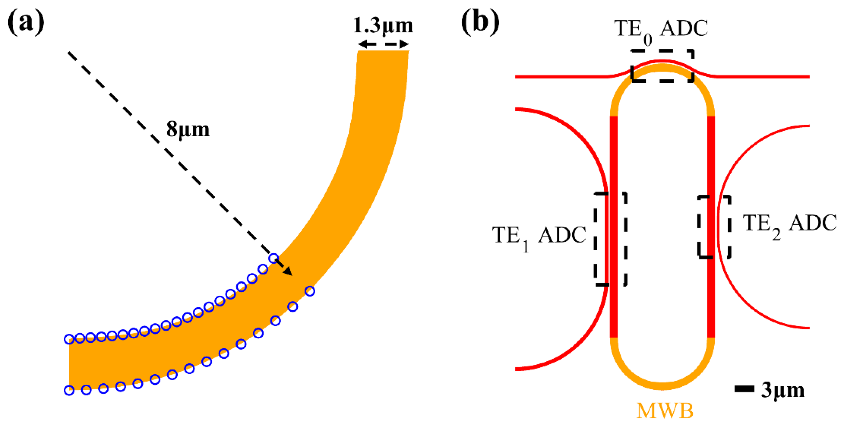
Figure 2.
T Simulation data for the optimized MWB with an effective radius of 8 μm.
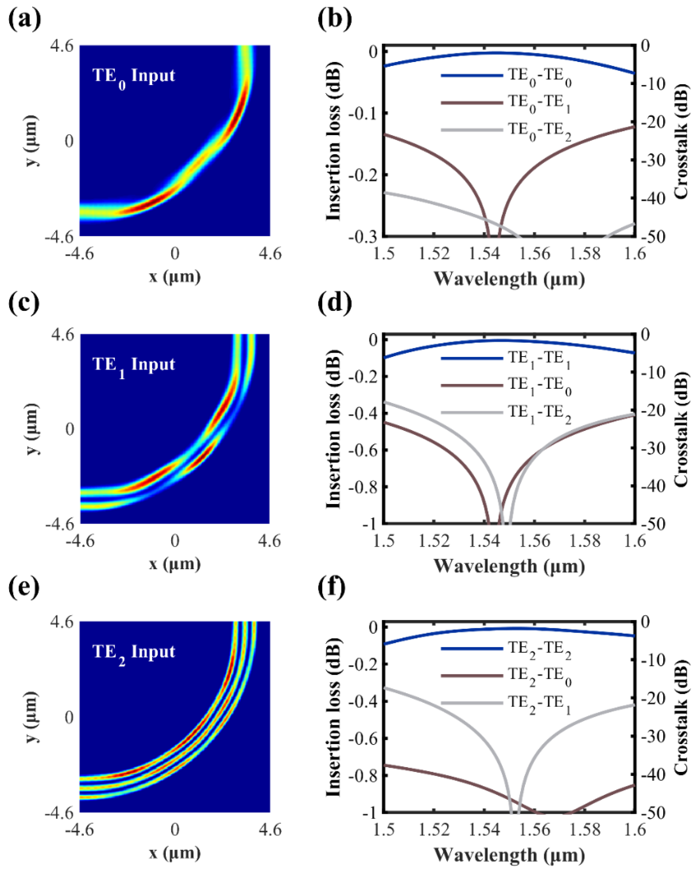
Figure 3.
Detailed schematics of ADC coupling regions of (a) , (b) and (c) modes.
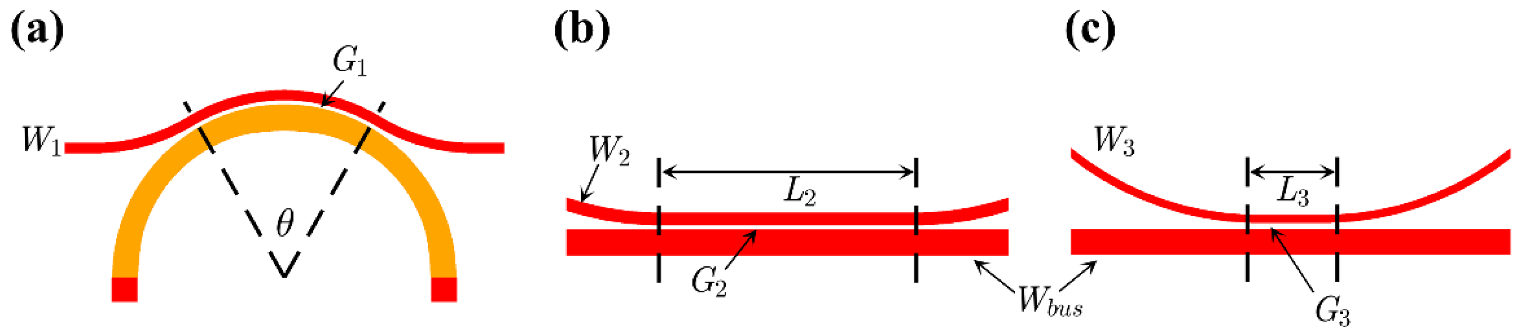
Figure 4.
Effective indices of , and modes for different (a)widths and (b)wavelengths.
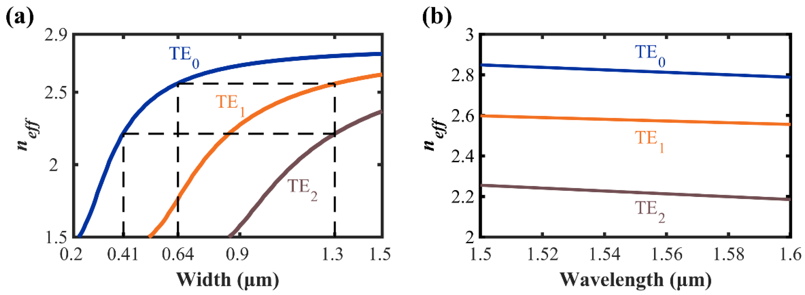
Figure 5.
(a) ADC , (b) ADC and (c) ADC electric field distributions for the multimode microring at 1.55 μm.
Figure 5.
(a) ADC , (b) ADC and (c) ADC electric field distributions for the multimode microring at 1.55 μm.
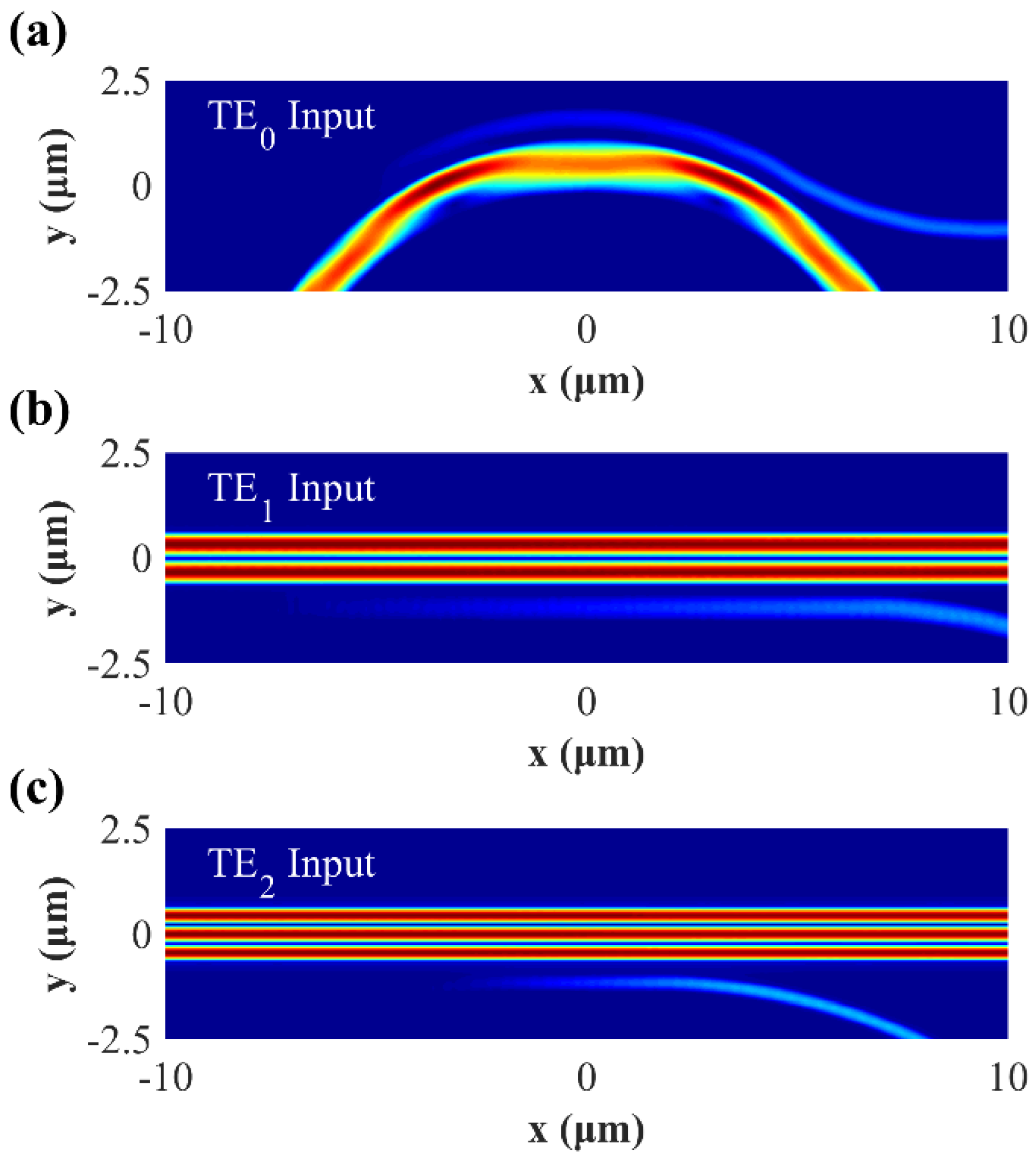
Figure 6.
The relationship between coupling coefficient and wavelength for (a) ADC, (b) ADC and (c) ADC under different attenuation factors.
Figure 6.
The relationship between coupling coefficient and wavelength for (a) ADC, (b) ADC and (c) ADC under different attenuation factors.
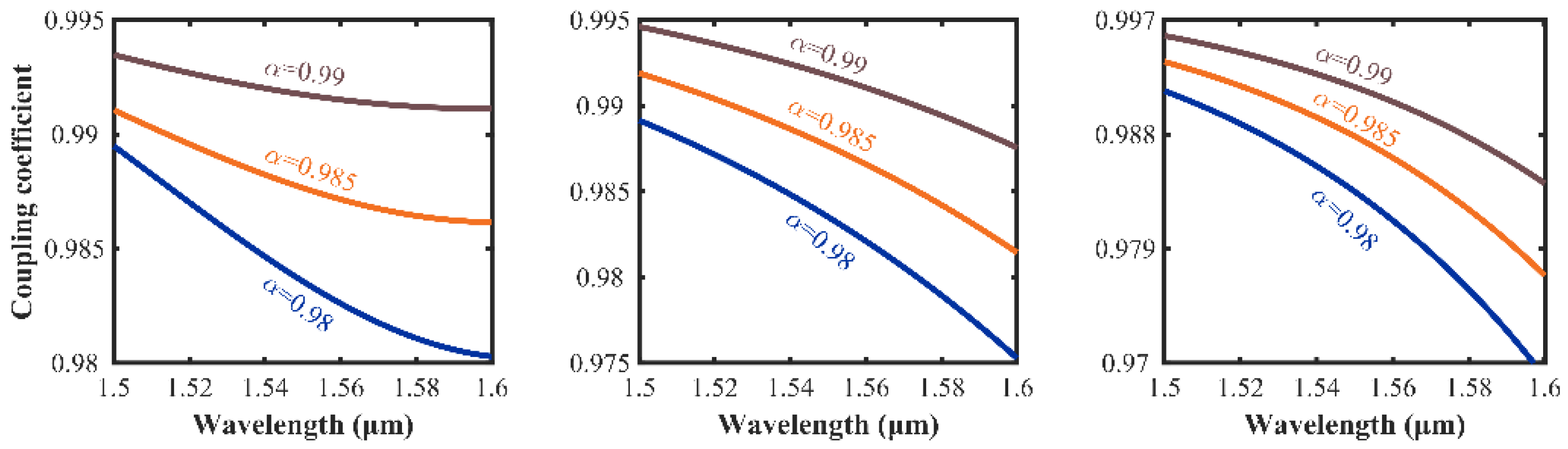
Figure 7.
Transmission spectrums of the MMRR for different attenuation factors and modes.
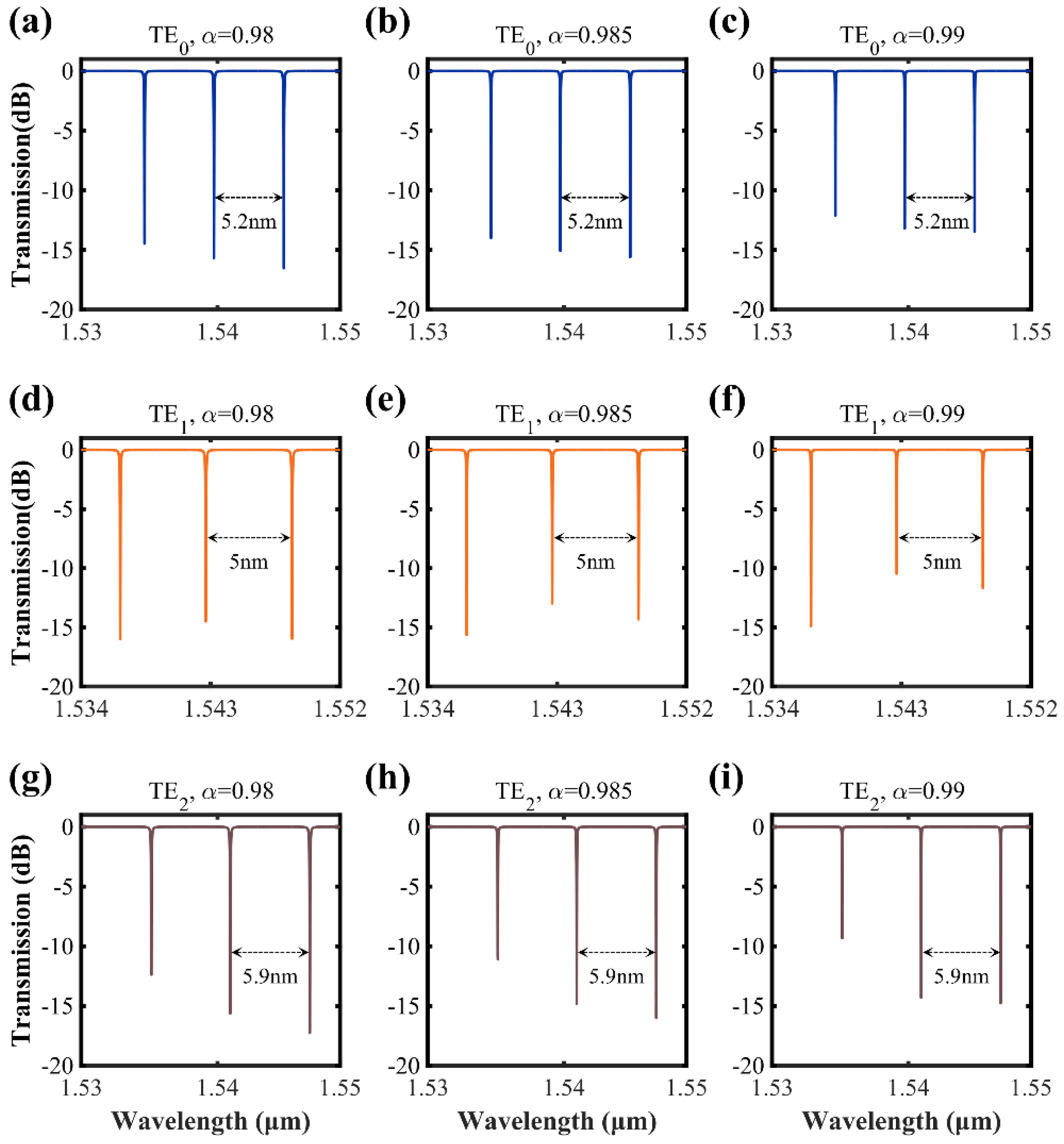
Figure 8.
Microscope images of the fabricated MMRR. (a) Overall picture for fabricated devices. (b) Grating coupler. (c) The zooming-in micrographs of MMRR.
Figure 8.
Microscope images of the fabricated MMRR. (a) Overall picture for fabricated devices. (b) Grating coupler. (c) The zooming-in micrographs of MMRR.
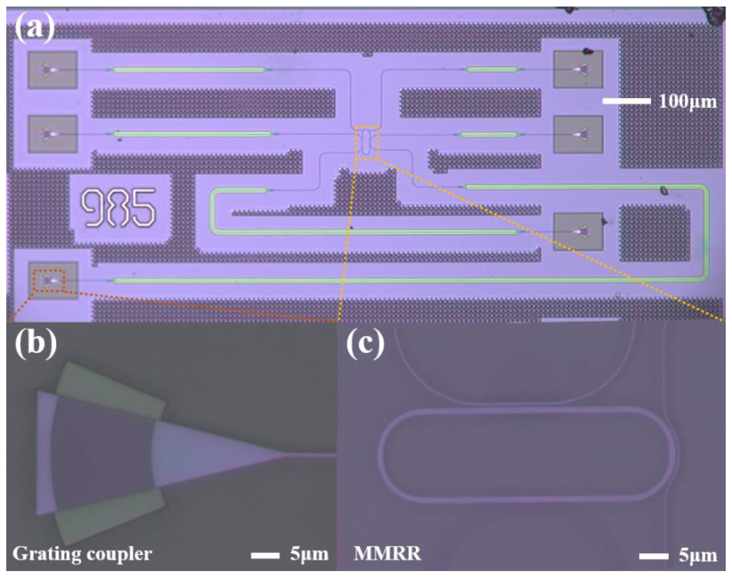
Figure 9.
Transmission spectrums of the fabricated MMRR. (a) - (c) Transmission spectrums for each mode. (d) - (f) The measured data (scattered dots) and Lorentzian fit curves (red lines) around resonant peaks for each mode.
Figure 9.
Transmission spectrums of the fabricated MMRR. (a) - (c) Transmission spectrums for each mode. (d) - (f) The measured data (scattered dots) and Lorentzian fit curves (red lines) around resonant peaks for each mode.
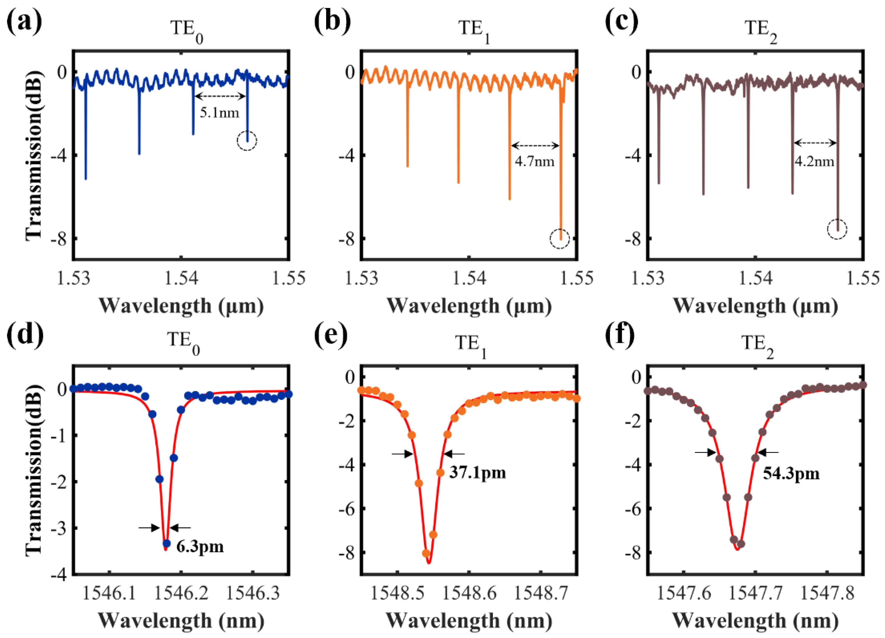

Table 1.
design parameters for three ADCs of the MMRR.
| α | θ (degree) | (μm) | (μm) |
|---|---|---|---|
| 0.98 | 62.57 | 12.74 | 3.27 |
| 0.985 | 51.4 | 10.57 | 2.3 |
| 0.99 | 42.86 | 8.03 | 1.28 |
Disclaimer/Publisher’s Note: The statements, opinions and data contained in all publications are solely those of the individual author(s) and contributor(s) and not of MDPI and/or the editor(s). MDPI and/or the editor(s) disclaim responsibility for any injury to people or property resulting from any ideas, methods, instructions or products referred to in the content. |
© 2025 by the authors. Licensee MDPI, Basel, Switzerland. This article is an open access article distributed under the terms and conditions of the Creative Commons Attribution (CC BY) license (http://creativecommons.org/licenses/by/4.0/).
Copyright: This open access article is published under a Creative Commons CC BY 4.0 license, which permit the free download, distribution, and reuse, provided that the author and preprint are cited in any reuse.


