
Submitted:
13 February 2025
Posted:
13 February 2025
You are already at the latest version
Abstract
This study explores the mechanisms responsible for the bandwidth reduction observed in Ge-on-Si photodetectors under high incident light power. We investigate the impact of the carrier-screening effect on the bandwidth through simulations, and we mitigate this effect by increasing the applied bias voltage. The increase in the concentration of photogenerated carriers leads to a reduction in the carrier saturation drift velocity, which reduces the bandwidth of the Ge-on-Si photodetector; this phenomenon is studied for the first time. The bandwidth is determined primarily by the carrier saturation drift velocity when the incident light power is below 2.5 mW, and the decrease in bandwidth that is calculated based on the decrease in carrier saturation drift velocity is consistent with the experimental results. However, when the incident light power exceeds 3 mW, both the carrier-screening effect and the reduction in the carrier saturation drift velocity contribute to the bandwidth reduction. This study provides a good theoretical guicdance for the design of high-power Ge-on-Si photodetectors.
Keywords:
Ge-on-Si photodetectors
; high-power optical signals
; bandwidth
; carrier-screening effect
; carrier saturation drift velocity
1. Introduction
Silicon photonics has been applied to optical communication and interconnection, and its applications in optical computing, optical sensing, and lidar have attracted extensive research interest [1,2,3]. As Ge-on-Si photodetectors are the key devices in the receiver, their performance plays an important role in the entire optical transceiver system. High sensitivity, large bandwidth and low dark current have been needed for the development of photodetectors [4,5,6].
For applications such as coherent optical communication, microwave photonics, and optical sensing, photodetectors must possess both high optical signal power and high operating frequency [7,8]. Currently, there are several papers on Ge-on-Si photodetectors that exhibit excellent frequency characteristics under high incident light power [9,10,11].
The bandwidth of Ge-on-Si photodetectors can decrease under high incident light power which limits their application [12,13,14]. The main reason for the decrease in bandwidth is the carrier-screening effect described in previous papers [15,16,17]. To reveal the reasons for the bandwidth decrease under high incident light power, this paper conducted simulations and experiments on the carrier-screening effect. To the best of our knowledge, the impact of the decrease in carrier saturation drift velocity, which is caused by a high concentration of photogenerated carriers, on the bandwidth of Ge-on-Si photodetectors has been studied for the first time. This provides theoretical support for the design of Ge-on-Si photodetectors for high-power applications.
2. Structure
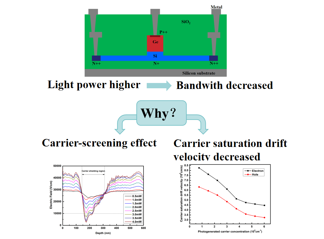
Figure 1 presents a cross-sectional diagram of a vertical PIN Ge-on-Si photodetector. This device is fabricated on a silicon on insulator (SOI) substrate, where the silicon layer functions as both the slab and waveguide regions. The silicon slab consists of both lightly and heavily doped areas. The lightly doped region, spanning from the rib waveguide to the electrode, is 1.5 μm wide and has a doping concentration of 1×10-17 cm-3. To ensure optimal ohmic contact between the slab and the metal electrode, a heavily doped contact region with a doping concentration of 1×10-20 cm-3 is incorporated. The thickness of the silicon slab is 60 nm. The width of the 220 nm thick rib waveguide is 1.5 μm, and the length is 10 μm. The doping concentration for the silicon rib is 1×10-15 cm-3; this concentration ensures the transport of high-concentration photogenerated carriers without significant light absorption. The germanium absorption layer is epitaxially grown on the silicon rib waveguide region with a thickness of 600 nm, and its width and length match those of the silicon rib waveguide region. For ohmic contact with the electrode, the top of the germanium absorption layer is heavily doped with a concentration of 3.8×10⁻¹⁸ cm-3.
The fabrication process began with an SOI wafer which then has its top layer of silicon etched, on which the nonetched area is the silicon waveguide and the shallow etched area is the slab region. Next, the wafer is lightly implanted with boron and then heavily implanted to form p-type ohmic contacts. The dopants in Si are activated using a rapid thermal annealing (RTA) process at 1030 °C for 5 s prior to germanium epitaxy. Ion implantation with phosphorus is then performed on top of the germanium layer to form the n-type ohmic contact area. After the cladding oxide is deposited, the fabrication process results in the formation of contact vias and aluminum interconnects. The defect density of the top silicon layer in the SOI is 3×104 cm-2, and the defect density of the epitaxial germanium layer is 7×104 cm-2.
An increase in the size of the germanium absorption region improves the level of high incident light power processing of the photodetector, but it increases the device’s capacitance, which reduces the bandwidth of the device.
The 3 dB bandwidth of the photodetector was measured using a setup comprising a vector network analyzer (VNA, KEYSIGHT PNA-X Network Analyzer N5247A) and a high-performance LiNbO3 modulator with a 40 GHz bandwidth. A precision DC power supply (KEITHLEY 2611A SYSTEM Source Meter) was used to apply the DC bias voltage to the photodetector through a bias-Tee.
We experimentally tested the bandwidth characteristic curves of the photodetector under various incident light powers at a -1 V bias voltage, as shown in Figure 2. The vector network analyzer emits electrical signals, which are amplified and loaded onto a 40G bandwidth lithium niobate modulator. The modulated optical signal enters the detector and is converted into an electrical signal, which is transmitted back to the vector network analyzer. Before testing, it is necessary to calibrate the entire link system to deduct errors generated by the instrument. A 1550-nm laser was utilized, and all the lasers mentioned in this paper operate within this wavelength range. To facilitate a clear understanding of the relationship between the bandwidth and incident light power, power is expressed in milliwatt (mW) units. The minimum incident light power was set to 0.5 mW, with increments of 0.5 mW, resulting in the following power levels: 0.5 mW, 1 mW, 1.5 mW, 2 mW, 2.5 mW, 3 mW, 3.5 mW and 4 mW. The corresponding optoelectronic bandwidths for each incident light power were determined to be 38.56 GHz, 37.33 GHz, 35.62 GHz, 32.34 GHz, 28.75 GHz, 23.41 GHz, 16.26 GHz and 6.52 GHz, respectively, as shown in Figure 2. The experimental results demonstrate that the bandwidth decreases with increasing incident light power, and the rate of the decrease becomes more pronounced at higher power levels. The relationship between the bandwidth and incident light power is further illustrated in Figure 2(b).
A major factor contributing to the reduction in bandwidth at high incident light power is the carrier-screening effect [12,13,14]. This carrier-screening effect occurs due to the rearrangement of photogenerated carriers under the influence of an external electric field. Photogenerated holes move in the direction of the applied electric field, whereas photogenerated electrons move in a direction opposite to the applied electric field. Then, the electrons and holes generate an internal electric field in the opposite direction to that of the external electric field. When the built-in electric field is superimposed with the external electric field, the electric field strength in the absorption region is weakened by the built-in electric field. When the concentration of photogenerated carriers is high, this effect is more pronounced. The carrier-screening effect leads to a decrease in the electric field strength in the absorption region, thereby reducing the migration rate of the carriers.
3. Experiments and Discussion
To quantitatively study the effect of carrier-screening on the bandwidth, we simulated the distribution of the internal electric field at different incident light power levels with the finite-difference time-domain (FDTD) method, and the results are shown in Figure 3. The region of the strongest light field in the germanium absorption region coupled with the evanescent wave is located 1.1 μm from the incident end [18]. Therefore, the simulation focused on the 1D electric field intensity in the germanium absorption region between the metal electrode and the silicon waveguide at this position. When a bias voltage of -1 V is applied, the minimum internal electric field intensity is approximately 2.34×10⁴ V/cm at an incident light power of 0.5 mW. As the incident light power increases to 4 mW, the minimum internal electric field intensity decreases significantly to 0.26×10⁴ V/cm. This indicates that the electric field in the photogenerated carrier region decreases substantially, whereas the field outside the carrier region increases. These results suggest a pronounced carrier-screening effect in the region where the electric field weakens.
The electric field intensity required to reach the saturation drift velocity of charge carriers in germanium is 0.97×10⁴ V/cm [19]. When the incident light power is less than 2.5 mW, although the carrier-screening effect reduces the local electric field intensity, it still allows the carriers to reach their saturation drift velocity. In other words, when the incident light power is below 2.5 mW, the decrease in electric field intensity due to the carrier-screening effect does not impact the device bandwidth. However, when the incident light power exceeds 3.0 mW, the carrier-screening effect begins to reduce the bandwidth.
The carrier-screening effect can reduce the electric field intensity in the photodetector at high incident light power levels. To counter this, we can increase the device’s internal electric field intensity by increasing the bias voltage, thereby reducing or even eliminating the impact of carrier-screening on the device bandwidth. The experimental results are presented in Figure 4.
We applied voltages of -2 V, -3 V, -4 V and -5 V for incident light powers of 0.5 mW and 4 mW, and we compared the resulting bandwidth characteristics to those observed at a -1 V bias. Given that the photodetector’s reverse breakdown voltage is -6 V, those test voltages were set within an appropriate range. At an incident light power of 0.5 mW, increasing the applied bias voltage from -1 V to -5 V resulted in almost no change in bandwidth. However, at an incident light power of 4 mW, increasing the bias voltage to -2 V, -3 V, -4 V or -5 V increased the bandwidth to 10.84 GHz, 15.03 GHz, 18.62 GHz or 18.62 GHz, respectively. When the bias voltage is increased to -5 V, the bandwidth characteristics remain almost consistent with those at -4 V and do not continue to increase. This observation is consistent with the simulation results shown in Figure 3. When the incident light power is 4 mW, the simulation results in Figure 3 show that the light absorption region has a significant carrier-screening effect. We eliminated the carrier-screening effect by increasing the bias voltage during the experiment, and the bandwidth of the photodetector was significantly improved. When the incident light power is 0.5 mW, the simulation results of the absorption region electric field show that the carrier-screening effect does not influence the carrier saturation drift velocity. In the experiment, by increasing the bias voltage to eliminate the carrier-screening effect, the bandwidth of the photodetector remains almost unchanged. The simulation results and experimental results show good consistency.
When the bias voltage is -5 V and the optical power is 4 mW, the photodetector bandwidth reaches 18.62 GHz, which remains lower than the 38.56 GHz bandwidth observed at an optical power of 0.5 mW with a -1 V bias. These experimental results indicate that at high incident light power, the carrier-screening effect reduces the device bandwidth by lowering the electric field intensity. However, the impact on the bandwidth is limited and significant only when the incident light power is less than 2.5 mW.
The increase in carrier concentration at high incident light power leads to a decrease in the carrier saturation drift velocity [20,21], which is another key factor that contributes to the reduction in bandwidth. A higher carrier concentration increases the scattering probability during carrier drift, thereby decreasing the carrier saturation drift velocity. An increase in the carrier concentration leads to an increase in the scattering probability, which mainly includes scattering between electrons and holes, carriers and lattices, phonons, and defects [22,23]. The scattering during carrier migration changes the direction of carrier movement, reducing the rate of carrier migration. Therefore, the rate of carrier movement along the electric field direction is reduced.
We experimentally measured the changes in the carrier saturation drift velocity at various photogenerated carrier concentrations using the Hall effect, as shown in Figure 5. The carrier saturation drift velocity in germanium was measured with an Ecopia HMS-3000 Hall tester. The sample was clamped onto a sample plate with a probe and injected with light through an optical fiber. At incident light powers of 0.5 mW, 1 mW, 1.5 mW, 2 mW, 2.5 mW, 3 mW, 3.5 mW and 4 mW, the corresponding concentration of photogenerated carriers in the high-field area of the germanium absorption region are 0.38×1016 cm-3, 0.75×1016 cm-3, 1.12×1016 cm-3, 1.51×1016 cm-3, 1.88×1016 cm-3, 2.26×1016 cm-3, 2.63×1016 cm-3 and 3.01×1016 cm-3, respectively. Since the electron saturation drift velocity is higher than that of holes, we focus primarily on the effect of a reduced hole saturation drift velocity on the device bandwidth. The corresponding hole saturation drift velocities are 6.33×106 cm/s, 5.94×106 cm/s, 5.51× 106 cm/s, 4.85×106 cm/s, 4.13×106 cm/s, 3.59×106 cm/s, 3.38×106 cm/s and 3.24×106 cm/s.
The 3 dB bandwidth is determined by the carrier transit time and RC constant [24,25]. The limit of the transit time can be described as follows:
where vh is the saturation hole drift velocity of the germanium, and d is the thickness of the intrinsic germanium film. The limit of the RC can be described by:
where R is the load resistance, and C is the capacitance. The 3-dB bandwidth can be estimated by:
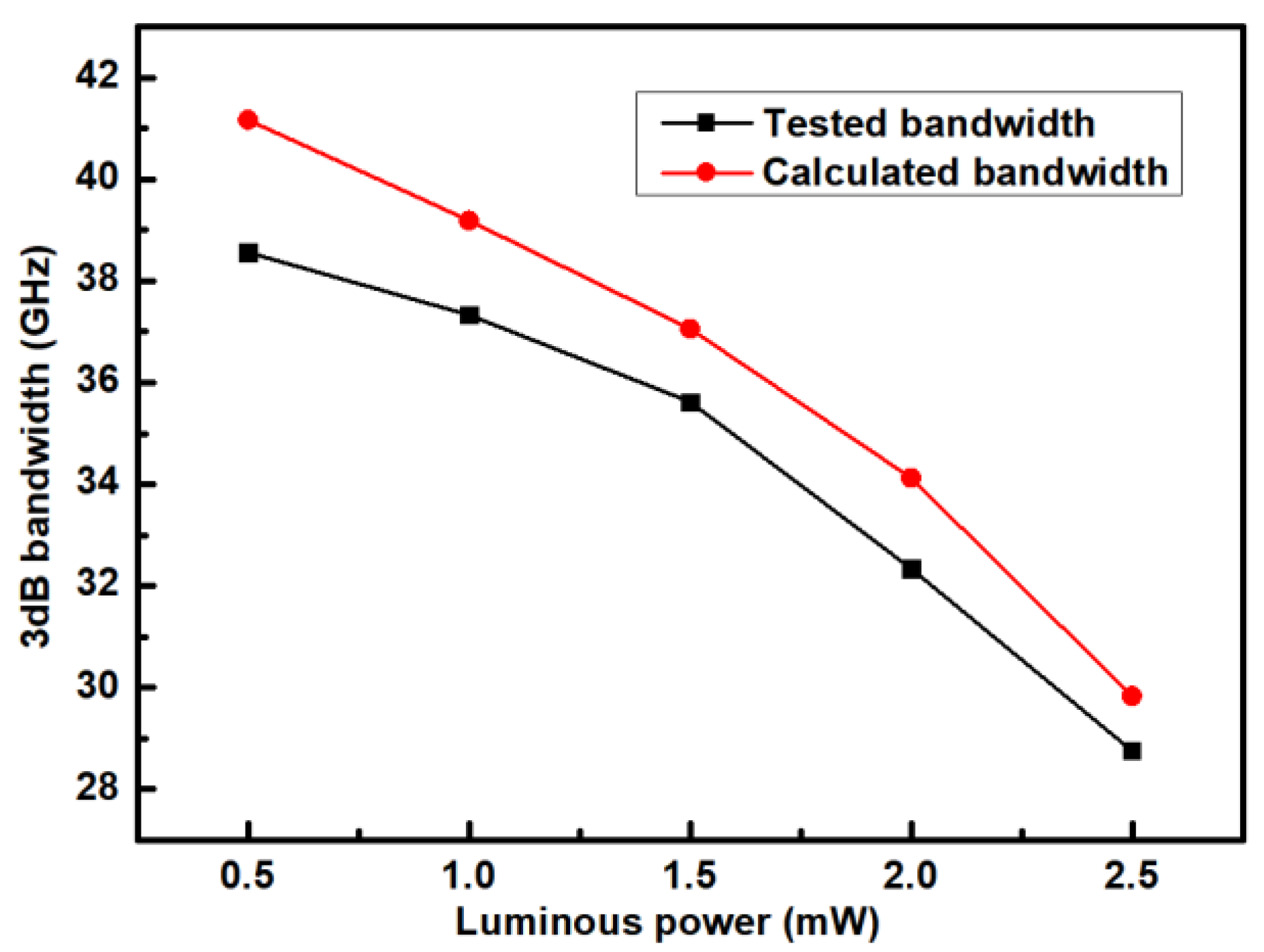
The measured series resistance was 618 Ω, and the capacitance was 4.5 fF, resulting in an RC-limited bandwidth of 57.23 GHz. Using the saturation hole drift velocity obtained from the Hall effect measurements experimentally, we calculated the bandwidth at various optical powers, as shown in Figure 6. This experimentally determined bandwidth serves as a reference and is consistent with the data presented in Figure 2. The bandwidth derived from the saturation hole drift velocity aligns closely with our experimental results, confirming that, for incident light powers less than 2.5 mW, the saturation hole drift velocity is the primary factor that influences the bandwidth. Notably, bandwidth values that are calculated using theoretical formulas tend to be slightly higher than those that are observed experimentally. This discrepancy is due primarily to losses and measurement errors during the testing process, which may affect the accuracy of the results. Overall, our findings highlight the critical role of the saturation hole drift velocity in determining photodetector performance under specific optical power conditions.
4. Conclusions
This work investigated the mechanism underlying the bandwidth reduction in Ge-on-Si photodetectors at high incident light power. According to experimental and simulation results, we conclude that the primary reasons for bandwidth reduction at high incident light power are the carrier-screening effect and the decrease in the carrier saturation drift velocity. We conducted multiple tests on the data in the paper, and the trend of the test results shows good consistency. Each data point used in our paper is the median of multiple tests.
For incident light powers below 2.5 mW, despite a notable carrier-screening effect, the electric field intensity across the absorption region remains sufficient for carriers to reach their saturation drift velocity. Thus, the carrier-screening effect has a minimal impact on the bandwidth of the photodetector in this range. Instead, the primary factor influencing bandwidth is the increased concentration of photogenerated carriers, which leads to a reduction in the saturation drift velocity of the holes.
When the incident light power exceeds 3 mW, the electric field intensity in the carrier-screening region becomes too weak to maintain the saturation drift velocity of the carriers. By increasing the applied bias voltage, we mitigate the effect of carrier-screening on the electric field intensity. However, the bandwidth remains lower than that observed at 0.5 mW. Therefore, an increase in the concentration of photogenerated carriers leads to a decrease in the saturation drift velocity of the holes, which is another significant factor in bandwidth reduction. This finding indicates that both the carrier-screening effect and the decrease in saturation drift velocity contribute to bandwidth reduction when the incident light power exceeds 3 mW.
The main reasons for the decrease in bandwidth under high incident light power are the carrier-screening effect and the decrease in carrier saturation drift velocity, both of which are caused by excessively high distributions of local carrier concentration. Therefore, in the design of Ge-on-Si photodetectors, owing to the coupling of evanescent waves, the light field in the germanium absorption region exhibits a strong weak alternating distribution. This leads to a carrier-screening effect and a decrease in the carrier saturation drift velocity in regions with strong light field distributions, thereby affecting the bandwidth. Optimizing the structural design to make the light field distribution in the germanium absorption region more uniform can effectively improve the frequency response characteristics of Ge-on-Si photodetectors under high incident light power.
Author Contributions
Conceptualization, Jin Jiang and Jishi Cui; methodology, Hongmin Chen; software, Fenghe Yang; validation, Xiumei Wang and Jishi Cui; formal analysis, Jin Jiang; investigation, Chunlai Li; resources, Jin He.; data curation, Jin He; writing—original draft preparation, Jin Jiang; writing—review and editing, Jishi Cui; funding acquisition, Xiumei Wang. All authors have read and agreed to the published version of the manuscript.
Funding
Please add: This research was funded by National Key Research and Development Program of China, grant number 2022YFB2803700, Natural Science Foundation of Fujian Province, grant number 2023J011030 and 2023J011029, the Fundamental Research Project of Shenzhen Science and Technology Fund, grant number JCYJ20220818103408017, JCYJ20220818103408018 and JCYJ20230807154759002, IER funding of PKU-HKUST Shenzhen-Hong Kong Institution: IERF202206.
Data Availability Statement
No new data were created or analyzed in this study. Data sharing is not applicable to this article.
Conflicts of Interest
The authors declare no conflicts of interest. The funders had no role in the design of the study; in the collection, analyses, or interpretation of data; in the writing of the manuscript; or in the decision to publish the results.
References
- Kumari K, Kumar S, Mehta M, et al. Laser-crystallized epitaxial germanium on silicon-based near-infrared photodetector[J]. IEEE Sensors Journal, 2022, 22(12): 11682-11689. [CrossRef]
- Jahangiri M, Sberna P, Sammak A, et al. Comparative Study of the Resolution of Ge-on-Si Photodetectors for $1\\mu\mathrm {m} $ Infrared Signals[C]//2022 IEEE 1st Industrial Electronics Society Annual On-Line Conference (ONCON). IEEE, 2022: 1-6.
- Chang C, Xie X, Li T, et al. Configuration of the active region for the Ge-on-Si photodetector based on carrier mobility[J]. Frontiers in Physics, 2023, 11: 1150684. [CrossRef]
- Liu X, Li X, Li Y, et al. High-Performance Cascaded Surface-Illuminated Ge-on-Si APD Array[J]. IEEE Electron Device Letters, 2022, 44(2): 205-208. [CrossRef]
- De Iacovo A, Mitri F, Ballabio A, et al. Dual-Band Ge-on-Si Photodetector Array With Custom, Integrated Readout Electronics[J]. IEEE Sensors Journal, 2022, 22(4): 3172-3180. [CrossRef]
- Cui J, Chen H, Zhou J, et al. High performance Ge-on-Si photodetector with optimized light field distribution by dual-injection[J]. IEEE Photonics Journal, 2022, 14(2): 1-4. [CrossRef]
- M.J. Byrd, E. Timurdogan, Z. Su, et al. Mode-evolution-based coupler for high saturation power Ge-on-Si photodetectors, Opt. Lett. 42 (4) (2017) 851–854. [CrossRef]
- Y. Zuo, Y. Yu, Y. Zhang, et al. Integrated high-power germanium photodetectors assisted by light field manipulation, Opt. Lett. 44 (13) (2019) 3338–3341. [CrossRef]
- Y Zhu, Z Liu, C Niu, et al., High-speed and high-power germanium photodetector based on a trapezoidal absorber,Opt. Lett. 47,(2022) 3263-3266. [CrossRef]
- Hu X, Wu D, Zhang H, et al. High-speed and high-power germanium photodetector with a lateral silicon nitride waveguide[J]. Photonics Research, 2021, 9(5): 749-756. [CrossRef]
- Li D, Yang Y, Li B, et al. High-Speed and High-Power Ge-on-Si Photodetector with Bilateral Mode-Evolution-Based Coupler[C]//Photonics. MDPI, 2023, 10(2): 142. [CrossRef]
- Hu X, Wu D, Zhang H, et al. High-speed lateral PIN germanium photodetector with 4-directional light input[J]. Optics Express, 2020, 28(25): 38343-38354. [CrossRef]
- Fard M M P, Cowan G, Liboiron-Ladouceur O. Responsivity optimization of a high-speed germanium-on-silicon photodetector[J]. Optics Express, 2016, 24(24): 27738-27752. [CrossRef]
- Chen G, Yu Y, **ao X, et al. High speed and high power polarization insensitive germanium photodetector with lumped structure[J]. Optics Express, 2016, 24(9): 10030-10039. [CrossRef]
- Byrd M J, Timurdogan E, Su Z, et al. Mode-evolution-based coupler for high saturation power Ge-on-Si photodetectors[J]. Optics letters, 2017, 42(4): 851-854. [CrossRef]
- Alasio M G C, Franco P, Tibaldi A, et al. Optical Power Screening Effects in Ge-on-Si Vertical Pin Photodetectors[C]//Annual Meeting of the Italian Electronics Society. Cham: Springer Nature Switzerland, 2022: 155-159.
- Sun C K, Tan I H, Bowers J E. Ultrafast transport dynamics of pin photodetectors at high-power illumination[J]. IEEE Photonics Technology Letters, 1998, 10(1): 135-137. [CrossRef]
- Cui J, Li T, Yang F, et al. The dual-injection Ge-on-Si photodetectors with high saturation power by optimizing light field distribution[J]. Optics Communications, 2021, 480: 126467. [CrossRef]
- Chen HT, Verheyen P, De Heyn P, Lepage G, De Coster J, Absil P, et al. High responsivity low-voltage 28-Gb/s Ge pin photodetector with silicon contacts. J Lightwave Technol (2015) 33(4):820–4. [CrossRef]
- Li Y, Clady R, Marshall A F, et al. Ultrafast carrier dynamics of a photo-excited germanium nanowire–air metamaterial[J]. ACS Photonics, 2015, 2(8): 1091-1098. [CrossRef]
- Golikova O A, Moizhes B Y, Stilbans L S. Hole mobility of germanium as a function of concentration and temperature[J]. Sov. Phys. Solid State, 1962, 3(10): 2259-2265.
- McLean T P, Paige E G S. A theory of the effects of carrier-carrier scattering on mobility in semiconductors[J]. Journal of Physics and Chemistry of Solids, 1960, 16(3-4): 220-236. [CrossRef]
- Ma N, Jena D. Charge scattering and mobility in atomically thin semiconductors[J]. Physical Review X, 2014, 4(1): 011043. [CrossRef]
- Sze S M, Li Y, Ng K K. Physics of semiconductor devices[M]. John wiley & sons, 2021.
- Cui J, Zhou Z. High-performance Ge-on-Si photodetector with optimized DBR location[J]. Optics Letters, 2017, 42(24): 5141-5144. [CrossRef]
Figure 1.
Cross-sectional diagram of the Ge-on-Si PIN photodetector.
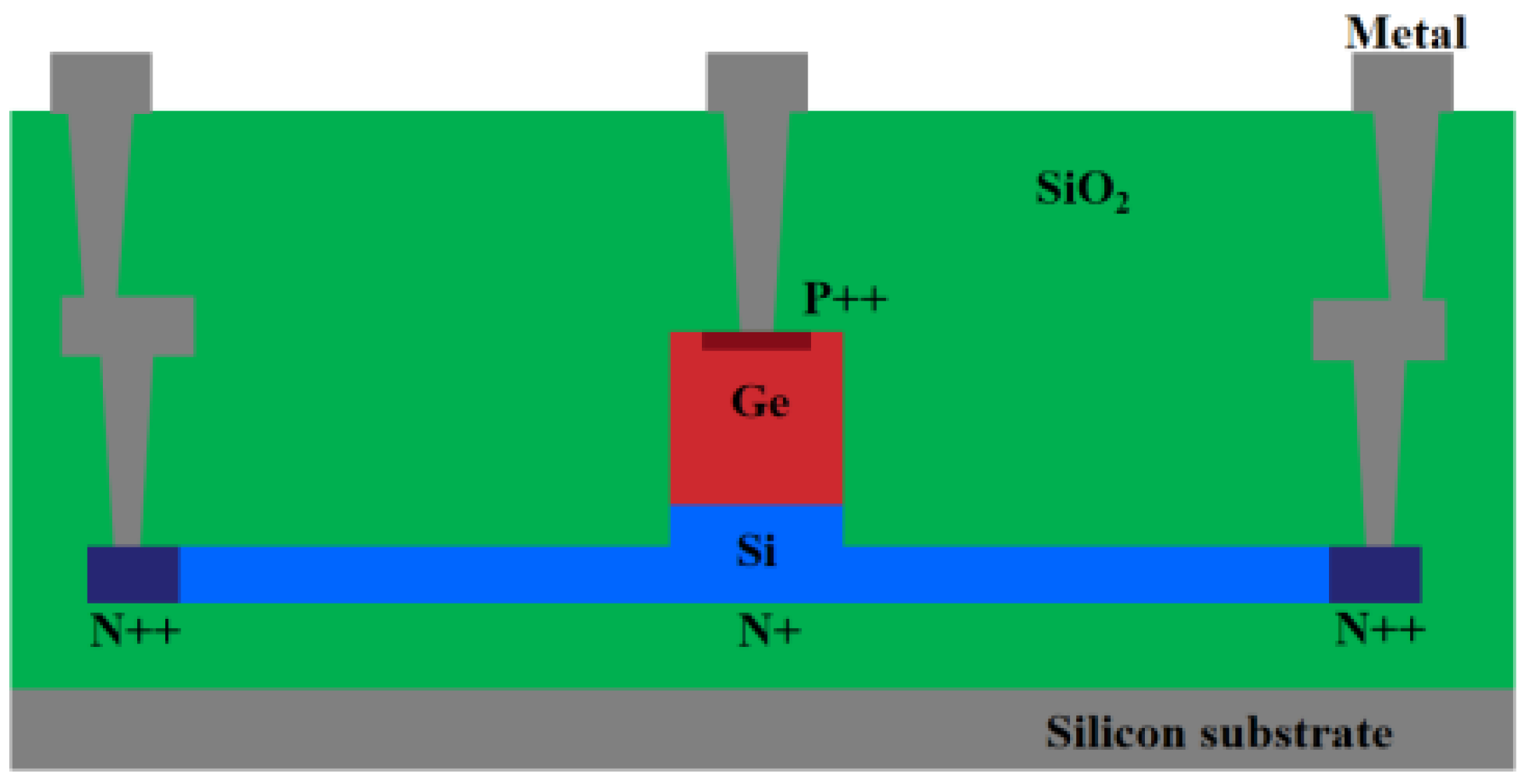
Figure 2.
(a) Normalized S21 traces of the photodetector under different incident light power levels, (b) 3 dB bandwidths of the photodetector under different incident light power levels.
Figure 2.
(a) Normalized S21 traces of the photodetector under different incident light power levels, (b) 3 dB bandwidths of the photodetector under different incident light power levels.
Figure 3.
The magnitude of the electric field in the germanium layer is measured along the metal contact and the silicon waveguide at a point 1.1 µm from the front edge of the absorber and at the center along the width.
Figure 3.
The magnitude of the electric field in the germanium layer is measured along the metal contact and the silicon waveguide at a point 1.1 µm from the front edge of the absorber and at the center along the width.
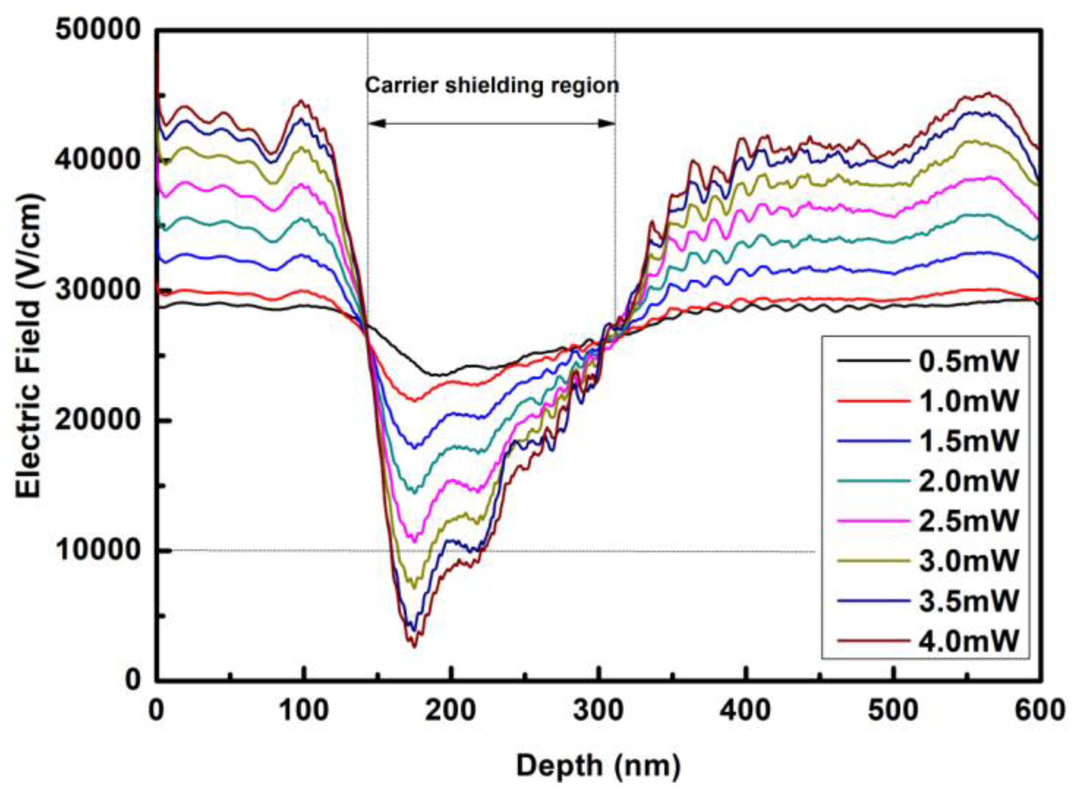
Figure 4.
Normalized S21 response of the photodetectors under different bias voltages at incident light powers of 0.5 mW and 4 mW.
Figure 4.
Normalized S21 response of the photodetectors under different bias voltages at incident light powers of 0.5 mW and 4 mW.
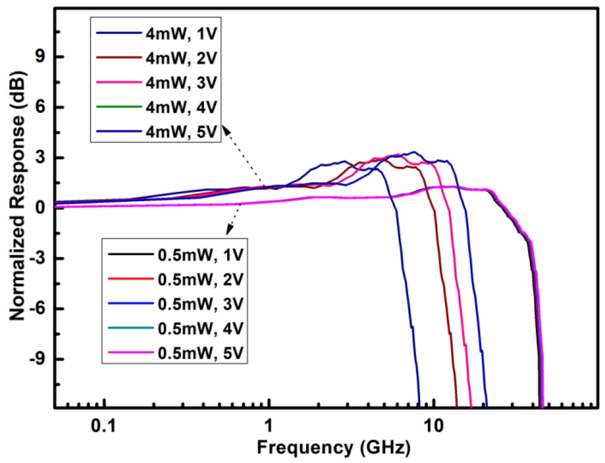
Figure 5.
Carrier saturation drift velocity versus photogenerated carrier concentration in the germanium layer according to the measured Hall effect.
Figure 5.
Carrier saturation drift velocity versus photogenerated carrier concentration in the germanium layer according to the measured Hall effect.
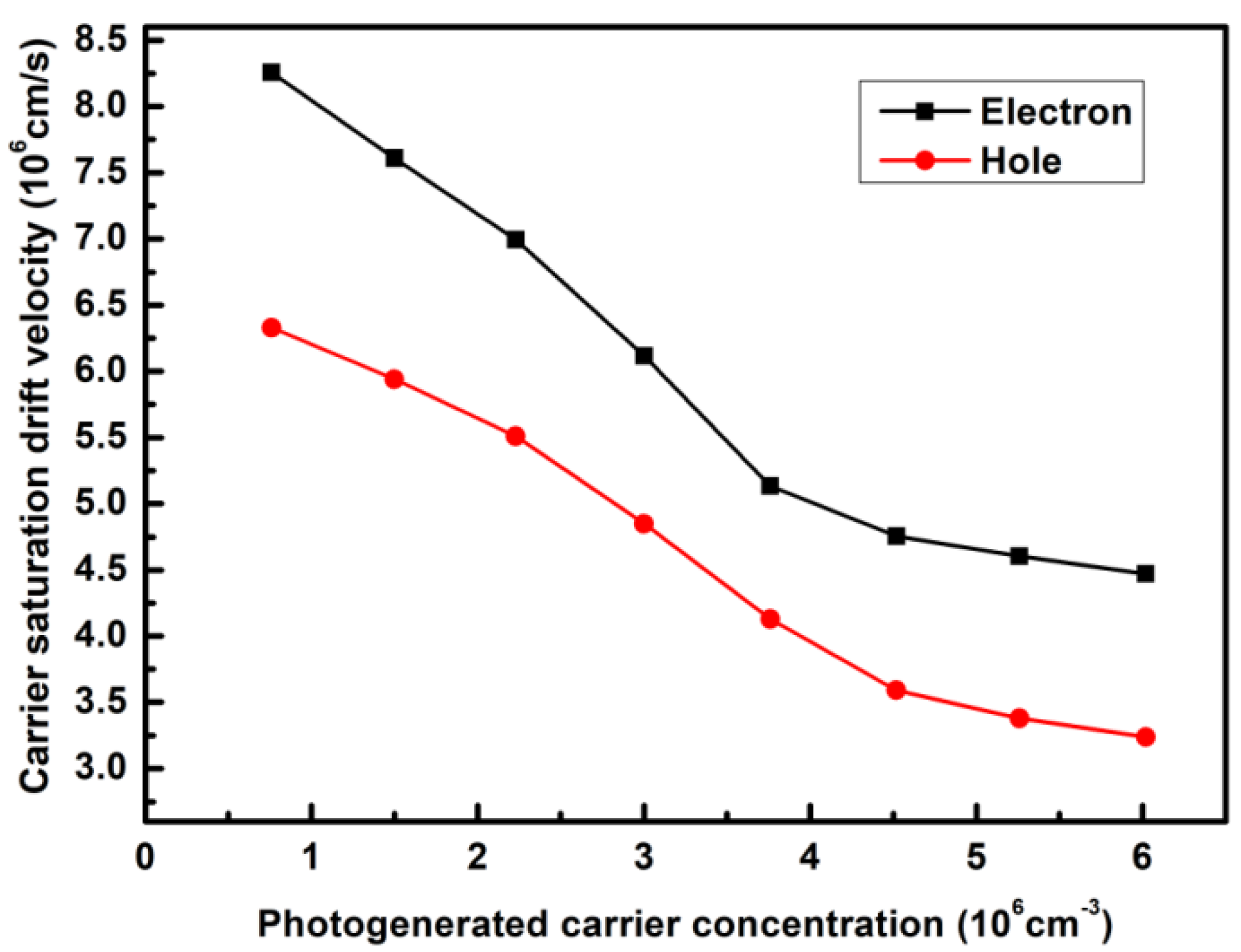
Figure 6.
The tested and calculated normalized S21 response of the photodetectors under different incident light powers.
Figure 6.
The tested and calculated normalized S21 response of the photodetectors under different incident light powers.
Disclaimer/Publisher’s Note: The statements, opinions and data contained in all publications are solely those of the individual author(s) and contributor(s) and not of MDPI and/or the editor(s). MDPI and/or the editor(s) disclaim responsibility for any injury to people or property resulting from any ideas, methods, instructions or products referred to in the content. |
© 2025 by the authors. Licensee MDPI, Basel, Switzerland. This article is an open access article distributed under the terms and conditions of the Creative Commons Attribution (CC BY) license (http://creativecommons.org/licenses/by/4.0/).
Copyright: This open access article is published under a Creative Commons CC BY 4.0 license, which permit the free download, distribution, and reuse, provided that the author and preprint are cited in any reuse.


