1. Introduction
The ability to scale intermittent semiconductor devices has continued to be a driving force in realizing integrated circuits that are smaller, faster, and more power-efficient in modern electronics. As technology advances into the sub-nanometer regime, traditional transistor technology like planar MOSFETs and FinFETs face critical challenges like short-channel effects (SCEs), problems with gate control, and higher power dissipation. These limitations preclude scaling transistors further, and alternative transistor architectures that yield better electrostatic control, improved performance, and scalability must be pursued [
1]. A gate-all-around (GAA) transistor is one promising solution to all these challenges. A GAA transistor has a gate surrounding the channel, providing more electrostatic control than conventional transistor structures such as FinFETs, where the gate is controlled from three sides. As the dimensions are scaled down even further, this enhanced control plays a crucial role in overcoming SCEs and device performance [
2]. The GAA-JLFET is among the most promising candidates for different GAA transistor configurations. In a conventional MOSFET, the current flows according to control by a well-defined p-n junction, while contrarily junctionless transistors control current flow based upon a continuous doping profile within the channel. The absence of a sharp junction boundary means that fabrication is simple, and there is no need for complex high-temperature processing and junction formation. Junctionless devices are less sensitive to the SCEs and are easily scalable with smaller dimensions. One strong cornerstone has been the material silicon, primarily used in fabrication, and the processing has matured and become highly cost-effective. The silicon-based GAA-JLFETs present an interesting case worth pursuing further since they may enable the reduction of the scaling limits and lead to better performance within the silicon CMOS ecosystem. In this paper, we explore the idea of GAA-JLFETs concerning silicon material and evaluate the advantages and disadvantages of applying this approach to next-generation semiconductor devices. In this paper, we take a step backward from that and aim to provide a comprehensive review of the basic GAA-JLFET principles, its performance, and how it overcomes the limits of conventional transistor design [
3].
As much as the scaling of transistor dimensions has continued unmoved, ad infinitum, according to Moore's Law [
4], this scaling has created fundamental difficulties with SCEs, leakage currents, and power dissipation in conventional MOSFETs. To overcome these problems, various multi-gate architectures, including so-called' Gate All Around' (GAA) transistors, are superior for the control of electrostatics and, thus, improve channel scaling. One of these is the JLFET, a novel device concept that eliminates the traditional pn junctions, is easy to fabricate and improves manufacturability [
5]. Unlike conventional MOSFETs that conduct current through a surface channel, JLFETs use bulk conduction, leading to mobility degradation and better carrier transport properties. Moreover, Cylindrical GAA JLFETs (CGAA-JLFETs) possess even better gate-to-channel control, thus effectively suppressing drain-induced barrier lowering (DIBL) and leakage currents, making them especially suitable for ultra-low power and high-frequency applications [
6].
Compound III-V semiconductor gallium arsenide (GaAs) has several advantages over silicon (Si) for electronic purposes, especially in high-frequency and optoelectronic devices. Since the electron mobility for GaAs is higher (~8500 cm²/V·s) than that of Si (~1400 cm²/V·s), transistor performance in drive current and switching speed is better for GaAs than for Si. Furthermore, GaAs possess a direct bandgap (1.42 eV at 300 K) and are very attractive for optoelectronic applications such as laser diodes and high-efficiency solar cells. However, due to its lower dielectric constant (ε = 12.9) compared to Si (ε = 11.7), weaker electrostatic control is obtained, leading to enhanced leakage current and SCEs in scaled devices. However, heterostructure engineering is a primary means of overcoming some of the shortcomings of GaAs-based transistors in low-power applications and their widespread exploration for high-speed, high-frequency, and RF applications. Recent research on GaAs-based GAA JLFETs has been related to utilizing superior transport properties of GaAs-based materials while optimizing the electrostatics using advanced doping techniques and high-k gate dielectrics [
7].
2. Theoretical and Simulation Framework
With a continued push toward smaller transistor sizes and enhanced device performance, semiconductors have been evolving fast in this field. Traditional MOSFETs face significant challenges at the sub-10 nm scaling regime, and alternative transistor architectures have been proposed. The class of junctionless transistors (JLTs) proposed by researchers does away with a conventional p-n junction in the channel, instead relying on a continuous doping profile. At the same time, this design promises reduced fabrication complexity and augmented electrostatic control in scaled devices. In parallel, GAA transistor architecture has emerged as a promising candidate for overcoming some of the limitations of FinFETs that are mainly limited by a lack of gate control on the channel. In the GAA structure, the gate not only encloses the channel on the top but all the exposed sides are covered with gates, making it easier to control electrostatically. Junctionless GAA transistors benefit from junctionless and GAA transistor designs, namely that junctionless transistors have fewer SCEs and better scalability [
8,
9].
Because of the improved electrostatic control over all corners of junctionless transistors, electrostatic GAA is one of the primary motivations for adopting this architecture. In traditional planar MOSFET, the gate only controls part of the channel, resulting in poor electrostatic control as the devices scale down. A three-dimensional structure with FinFETs was introduced to overcome this issue; however, as the channel length continues to scale, SCEs and DIBL remain of concern. Junctionless GAA transistors have their gate surrounding the channel, providing superior electrostatic control and eliminating SCEs. According to research from Hossain et al., this superior control causes a reduced threshold voltage variation and steeper subthreshold slope (SS), which are standard for better switching characteristics. A significant reduction in subthreshold leakage currents and a higher on/off ratio than traditional and GAA junctionless transistors have been demonstrated [
10].
The simplified fabrication process can also be another significant advantage of GAA-JLFET. Conventional devices create p-n junctions in the channel, but GAA-JLFET devices have uniform doping profiles in the channel. As a result, the fabrication complexity is significantly reduced in junction formation, high-temperature processing, and doping profile control. Ghosh et al. have shown that GAA-JLFET devices could be fabricated using relatively simpler process flows on silicon-on-insulator (SOI) wafers, which provide better electrostatic isolation and easier control of the channel conductivity. The continuing low cost, well-understood manufacturing processes, and superior mechanical properties of silicon continue to make it the most frequently used semiconductor fabrication material for submicron devices. Silicon has relatively high carrier mobility and is a well-known bandgap in terms of electrical properties. It is an ideal candidate for most semiconductor devices. Nevertheless, with the ongoing scaling of the transistor size, the performance of silicon-based devices is limited due to SCEs and carrier mobility [
11].
In recent years, the potential of silicon concerning junctionless GAA devices has been investigated in works by Srivastava et al. Silicon-based junctionless GAA transistors have significant advantages over conventional planar MOSFETs and FinFETs in terms of reduced SCEs, saturation current, and better scalability. Although silicon is a well-accepted material, the use of silicon in Junctionless GAA transistors is limited by carrier mobility limitation [
12]. Compared to materials such as germanium, III-V compounds (e.g., InGaAs), and graphene, silicon has lower electron mobility and smaller current drive capabilities of devices. To tackle this issue, A. Kumari et al. presented strained silicon or silicon-germanium alloy as carriers of carrier mobility improvement. Improvements in velocity and, thus, drive current can be achieved with strained silicon created by introducing tensile or compressive strain in the material. Yet, applying strain to silicon devices often results in additional complexity and challenges, including strain-mediated mechanical stress management during fabrication and strain-sensitive interface defects [
13].
Junctionless GAA devices are widely regarded as an excellent candidate for commercialization and ideal for SOI wafer fabrication. Insulation of the channel from the substrate enables better control over the channel and reduces parasitic capacitance, enabling better device performance. In addition, the insulating layer supplies better electrostatic isolation, which is essential for shrinking GAA-JLFET devices without degrading performance. Dixit et al. have shown that using SOI wafers also allows for higher performance of Junctionless GAA devices by preventing current leakage through the substrate and providing a cleaner current path [
14]. However, precise patterning of the gate and channel affects the performance of scaled-down junctionless GAA devices. As device dimensions approach the nanometer scale, traditional photolithography techniques operate near their resolution limits. As a result, researchers have been investigating higher-resolution lithography techniques, such as extreme ultraviolet (EUV) lithography and nanoimprint lithography (NIL). For example, Results showed the use of NIL to fabricate high-quality nano-wire structures in GAA-JLFET. As a result, NIL offers excellent advantages over conventional photolithography; NIL produces smaller feature sizes and is, therefore, a promising candidate for the future fabrication of GAA-JLFET [
15].
The performance of Junctionless GAA devices is heavily dependent on the channel doping profile. These devices require the doping to be uniform across the channel to ensure continuous bandwidth and avoid separate p-n junctions. Uniform doping profiles have been attempted using ion implantation and in-situ doping techniques. Nevertheless, doping concentration gradients and the diffusion of dopants during high-temperature processing impeded the precision of the doping profile. It has been recently proven that atomic layer doping (ALD) techniques can improve the doping uniformity in GAA-JLFET. Numerous research studies have been conducted to compare Junctionless GAA transistors with conventional FinFETs and planar MOSFETs to demonstrate the electrostatic control, scalability, and reduction of the SCEs of Junctionless GAA transistors [
16]. For instance, they showed that junctionless GAA transistors exhibit better threshold voltage stability given improved electrostatic control, reduced short channel effects resulting in lower leakage currents and better on/off current ratios, and successful scaling down to the 5 nm node with little performance degradation. Other studies, for example, reported that Junctionless GAA transistors are scaled further and may confront impediments to high leakage currents and power efficiency, particularly with silicon-based devices. Though significant advancements have been achieved in exploring the application perspective of GAA-JLFET, certain issues are still largely unaddressed, namely material constraints, technological issues, and scaling problems [
17].
3. Methodology and Device Structure of JLFET
For efficient prediction of the device's performance in nanoscale regimes, the cylindrical GAA-JLFET (CGAA-JLFET) also requires analysis. Poisson's equation in cylindrical coordinates describes the electrostatic behavior of these transistors, that is, the potential distribution within the channel. Next, the threshold voltage is derived from solving the 2D Laplace equation with the proper boundary conditions, including the doping concentration effect, oxide thickness, and channel radius. The analysis of SCEs like DIBL and subthreshold slope (SS) degradation is presented by the potential to explore the weaker electrostatic integrity in the case of GaAs's lower dielectric constant-based transistors. In addition, the drain current characteristics are modeled using the drift-diffusion transport equation, and the higher carrier mobility of GaAs leads to higher drive currents, although they suffer from greater off-state leakage. An assessment of combining different channel lengths and optimized doping profiles to alleviate SCEs, improve the subthreshold performance, and decrease the leakage currents in GaAs-based CGAA-JLFETs is presented. Before this work, theories and experiments regarding Si and GaAs-based JLFETs were developed. This mathematical framework incorporates this prior work, fully compares Si and GaAs-based JLFETs, and provides key insight into the application space of these devices for low-power and high-frequency applications [
18,
19,
20]. The mathematical solutions for drain current under various bias conditions are shown in
Table 1 and
Table 2.
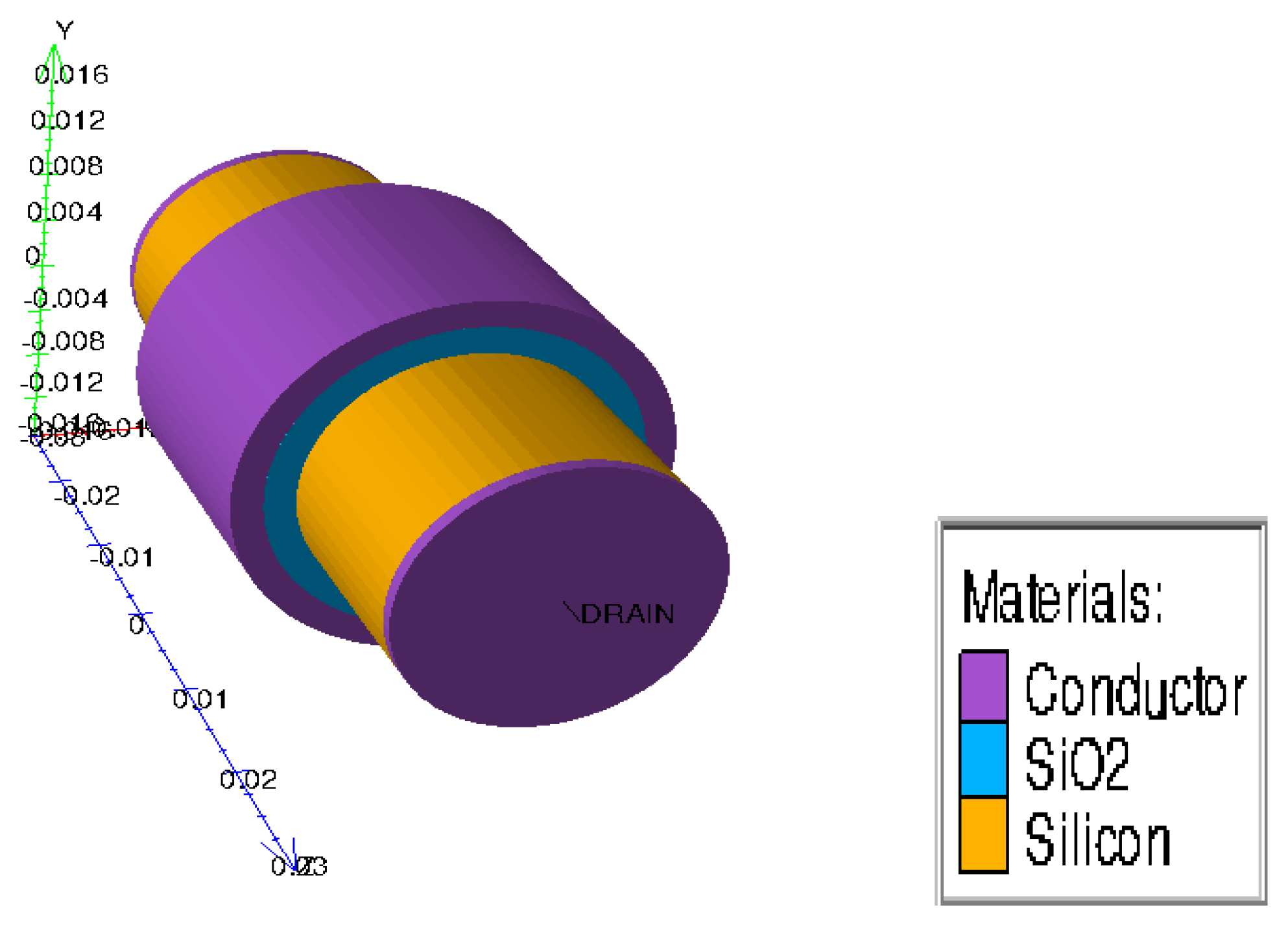
In our work, we have performed a detailed analysis of silicon-based three-dimensional JLFET with cylindrical gate-all-around architecture. As shown in
Figure 1, this proposed architecture has been comparatively studied with varying gate lengths of 10, 20, 30, 40, 50, and 60 nm with a constant radius of 14 nm. The ITRS road map has guided geometrical settings and mesh design, and finally, this crucial task has been provided with proper technology nodes and feature sizes as needed. With the help of extensive 3D simulations done in SILVACO TCAD tools, it is shown that the presented device exhibits better performance than the conventional MOSFETs. The 3D cylindrical design has radius mesh (R in µm), angle mesh (A in degrees), and length mesh (Z in µm) and five regions of silicon (semiconductor), SiO
2 (insulator), 3 regions of conductor (Metal). The coordinates for the cylindrical structure involved three electrodes: drain, source, and gate. The device parameters of the proposed device are noted in
Table 3.
The Shockley-Read-Hall and AUGER recombination models were used to analyze recombination effects for high current densities. NEWTON and GUMMEL models were incorporated into equations with coupled and decoupled forms. This paper describes the simulation of the electrical characteristics of novel transistor JLFET with gate-all-around architecture using ATLAS 3-D device simulator for different channel lengths.
4. Result and Discussions
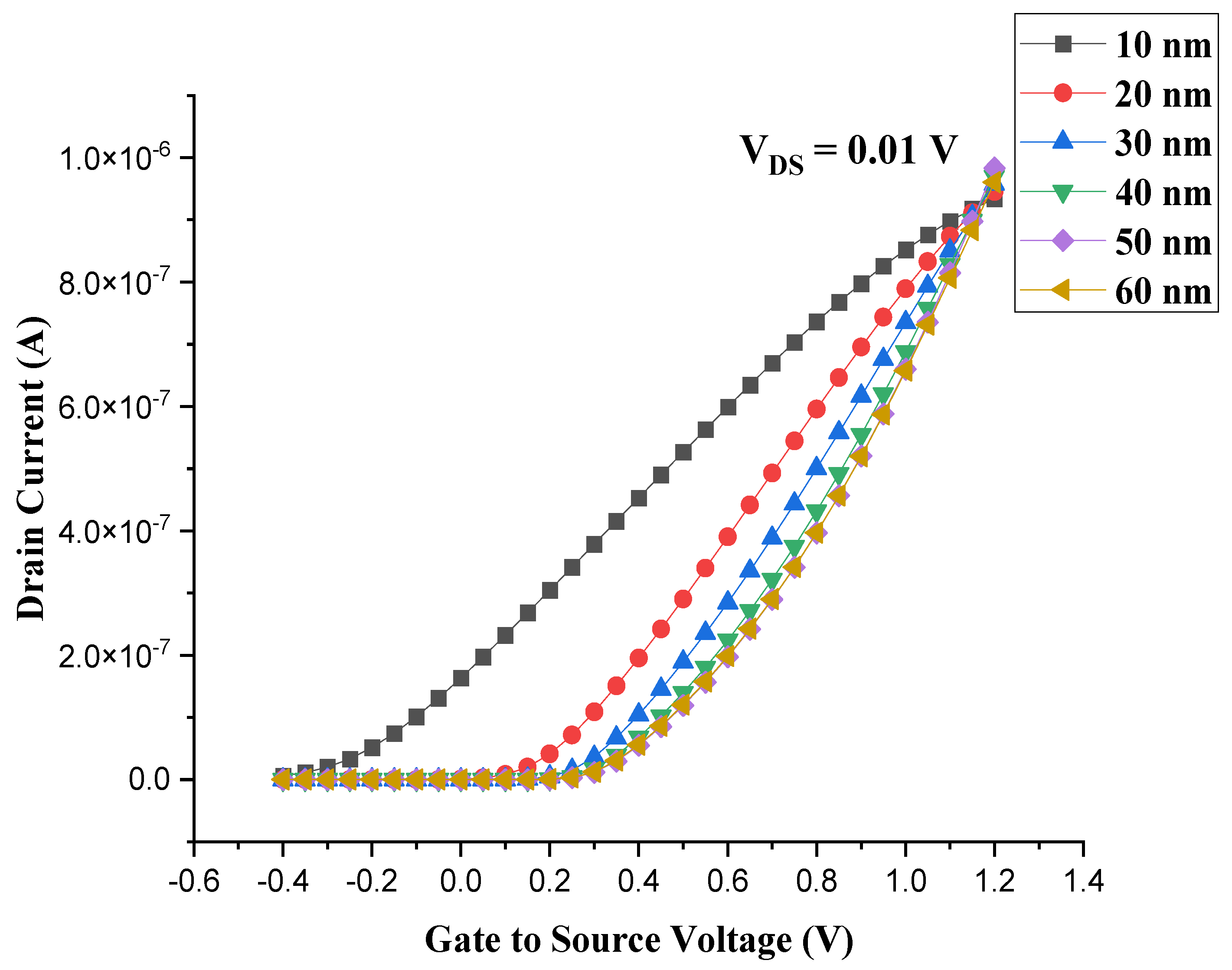
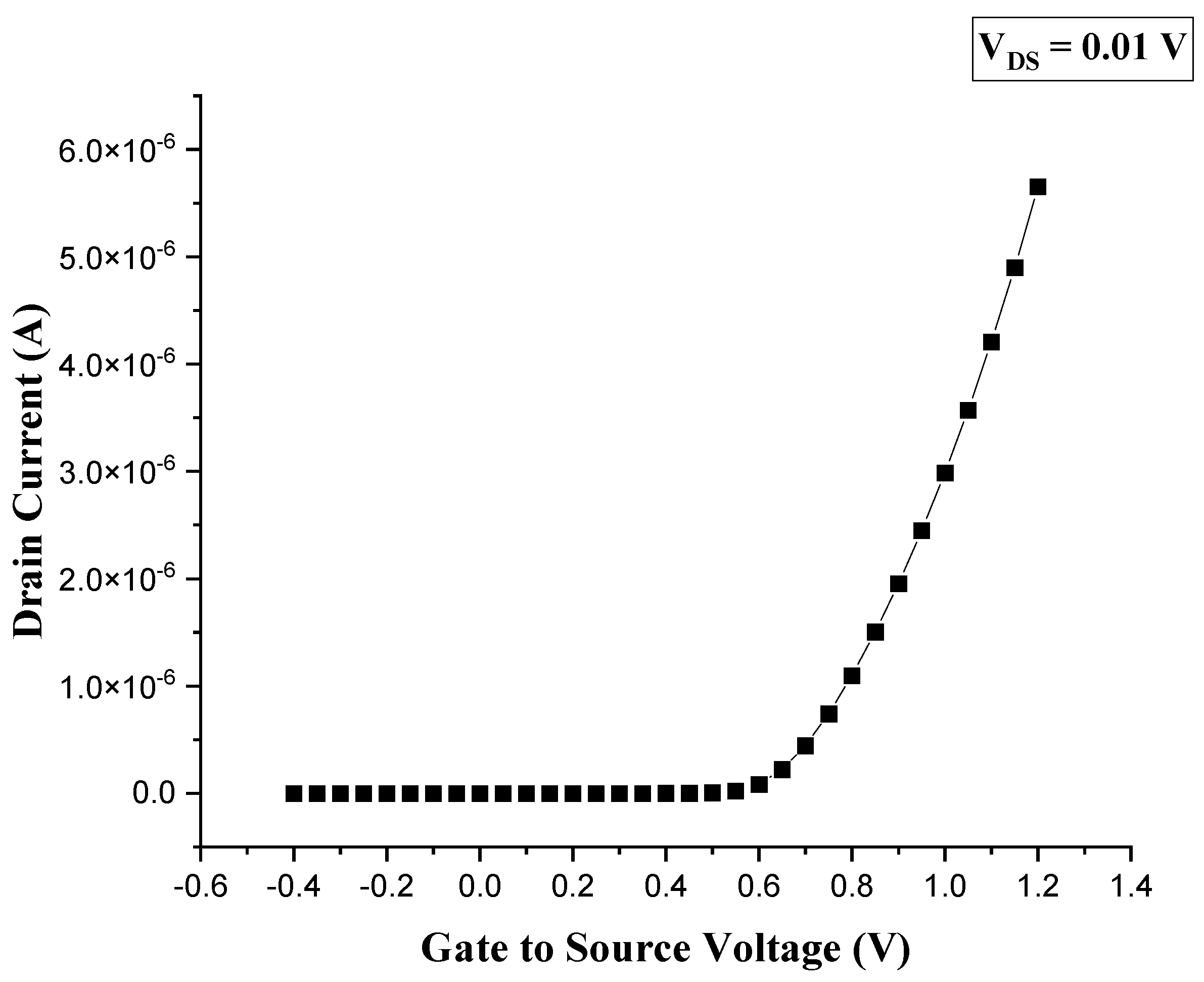
Figure 2 presents the simulated transfer characteristics of CGAA-JLFET for different channel lengths ranging from 10 nm to 60 nm, and P+ Polysilicon has been used to fulfill the requirement of high gate workfunction to achieve appropriate V
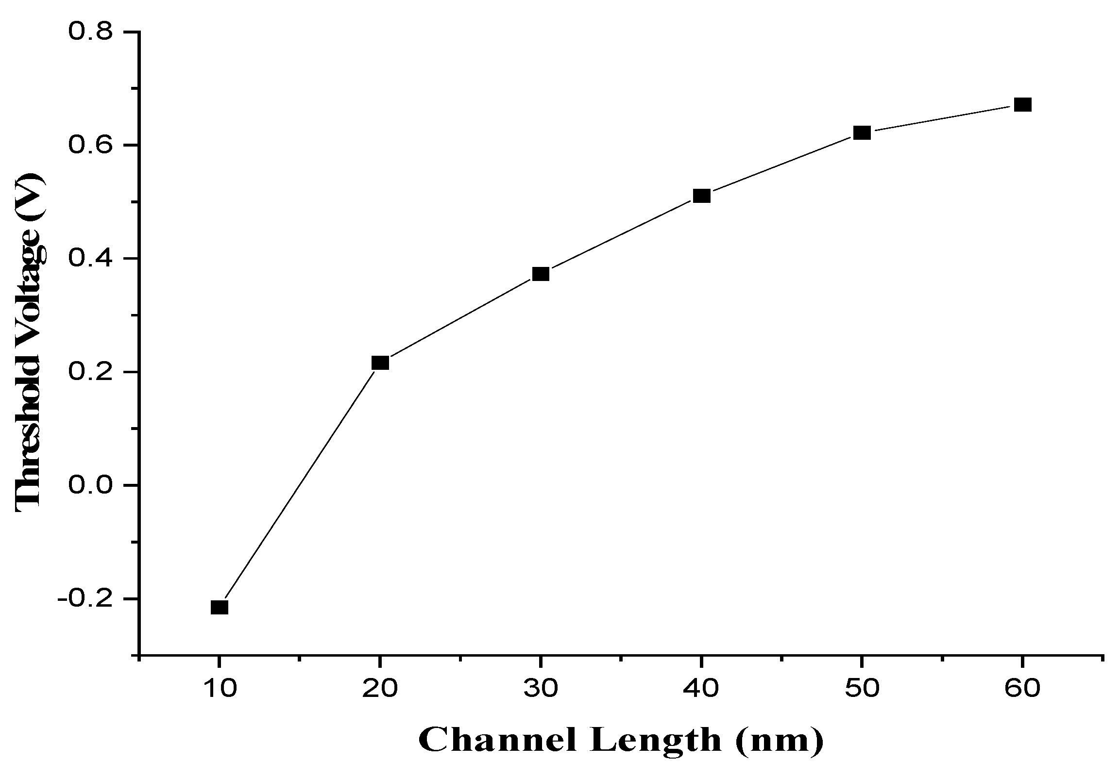
TH value. The threshold voltage value decreased as the channel length decreased, as shown in
Figure 3. These I
D-V
GS characteristics of the CGAA-JLFET have been plotted at V
DS = 0.01 V, spanning a range of V
GS from -0.4 to 1.2 V. The threshold voltages for different channel lengths have been observed to be V
th = -0.21461 V (at 10 nm), 0.216574 V (at 20 nm), 0.37356 V (at 30 nm), 0.511143 V (at 40 nm), 0.622054 V (at 50 nm) and 0.671832 V (at 60 nm).
The characteristics and results of a silicon-based CGAA-JLFET show the behavior of the drain current as a function of the gate-to-source voltage (V
GS). The transfer curve of a JLFET often rises sharply above when V
GS crosses the threshold voltage (V
TH) and then saturates in the on-state. This device has a steep subthreshold slope, showing that switching is efficient. As we decrease the channel length, SCEs arise, which force the threshold voltage (V
TH) to drop; hence, it is more sensitive to a change in V
DS. As a result, leakage current rises, and the I
on/I
off ratio decreases, leading to compromised device switching efficiency [
22]. Compared to other inversion devices, SCEs are less common in JLFETs. Equation 1 explains how the space charge area connected to the junctions (designated as SCE in Equation 1) and the expansion of the drain space charge region with drain voltage (designated as DIBL in Equation 1) cause the threshold voltage to decrease in the junction or other conventional devices.
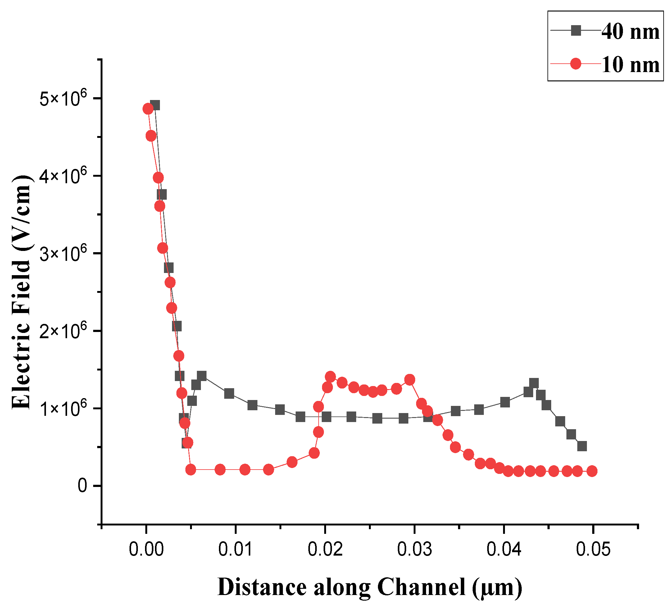
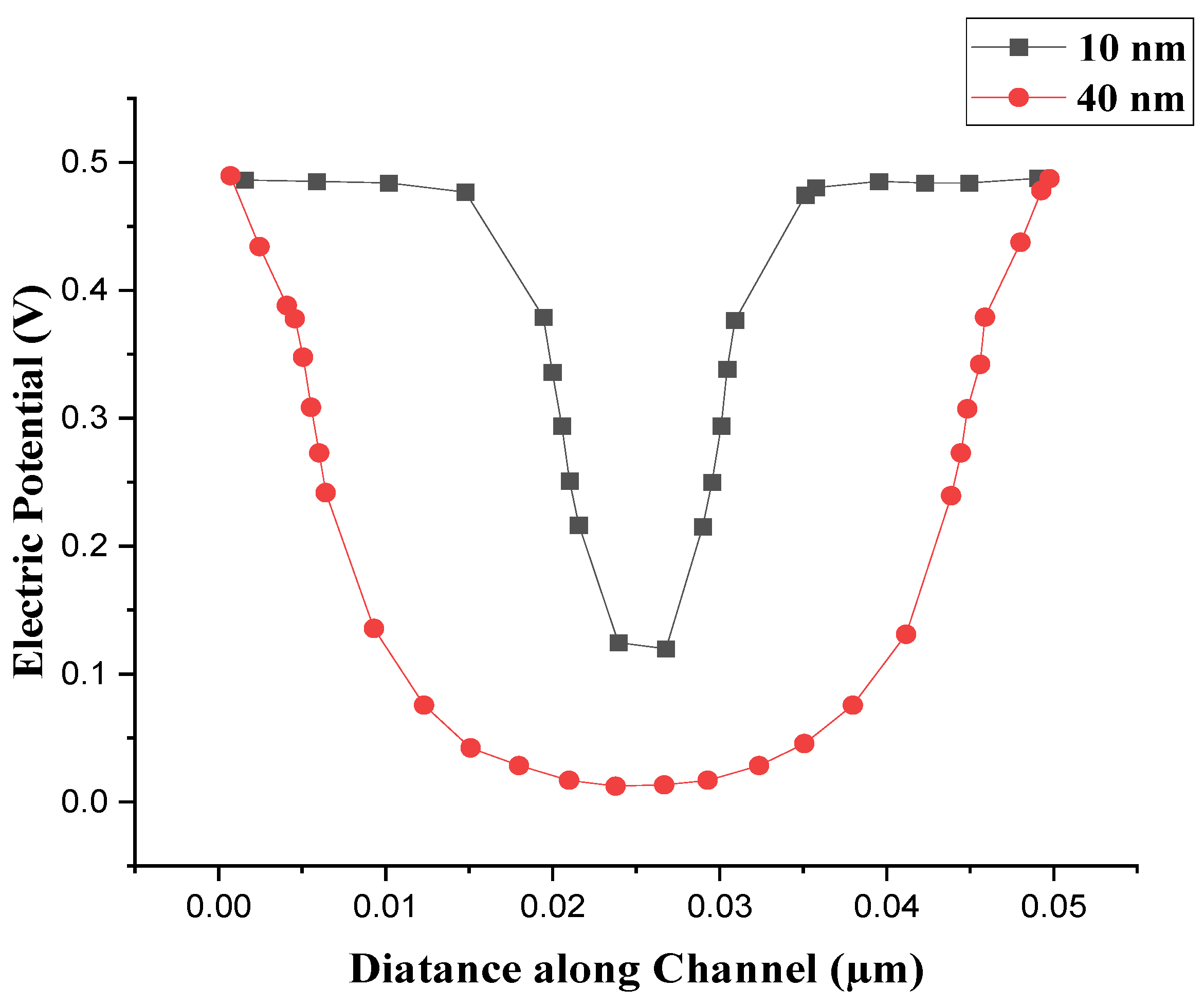
Figure 4 shows the plot of the electric field distribution versus the distance from the gate electrode along the nano-wire for 10 nm and 40 nm CGAA-JLFET, respectively. Scaling and SCEs significantly differ in electric field distribution for a 10 nm and 40 nm CGAA-JLFET. When scaled to a 10 nm channel length, the electric field across the channel is highly concentrated near the source and drain regions, where the variations are sharp due to the strong DIBL and punch-through effects. Because of this scale, however, the gate electrostatic control becomes weak, resulting in a non-uniform electric field at the channel ends where the field is higher. However, for this case of the 40 nm channel length, the electric field distribution is uniform over the channel compared to that of the 10 nm channel, with smaller SCEs. The gate-to-channel electrostatic coupling is stronger, allowing better channel control. In both cases, the CGAA-JLFET structure helps overcome some of the SCEs by providing better gate control on the channel, but as the channel length reduces, the field becomes localized, and device performance becomes more dependent on higher leakage currents and switching efficiency [
23].
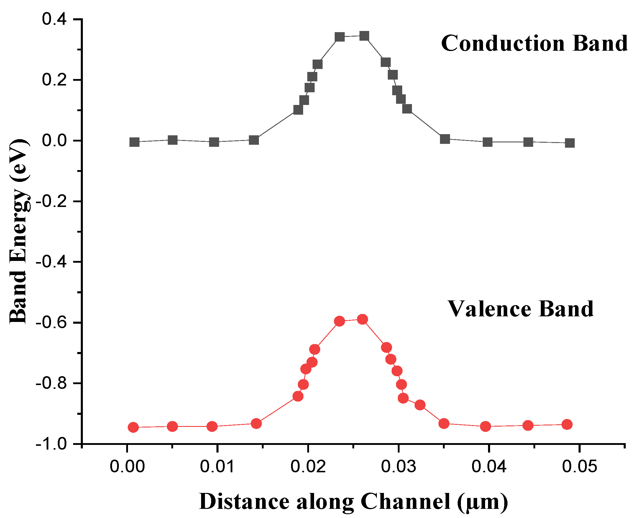
Figure 5 and
Figure 6 show the energy band diagrams of 10 nm and 40 nm CGAA-JLFET, respectively. The energy band diagram consists of a conduction band and a valence band. An energy band diagram for 10 nm and 40 nm CGAA-JLFET shows the effect of gate voltage, channel length, and SCEs on the conduction and valence bands. The band bending in the source and drain regions for the 10 nm CGAA-JLFET is due to DIBL and quantum confinement effects and is very significant. More pronounced in shorter channels, the strong electrostatic influence of the drain on the channel leads to a very steep band bending and, thus, reduced control over the carrier transport across the channel. In this case, the Fermi level near the source and drain is more affected, which causes an increase in leakage current. The energy band diagram shows a sharper band bending along the channel length for the 40 nm CGAA-JLFET, indicating relatively less severe SCEs. The energy bands demonstrate a smoother transition from the source to the drain, and the electrostatic control from the gate is more effective and, therefore, more concentrated [
24].
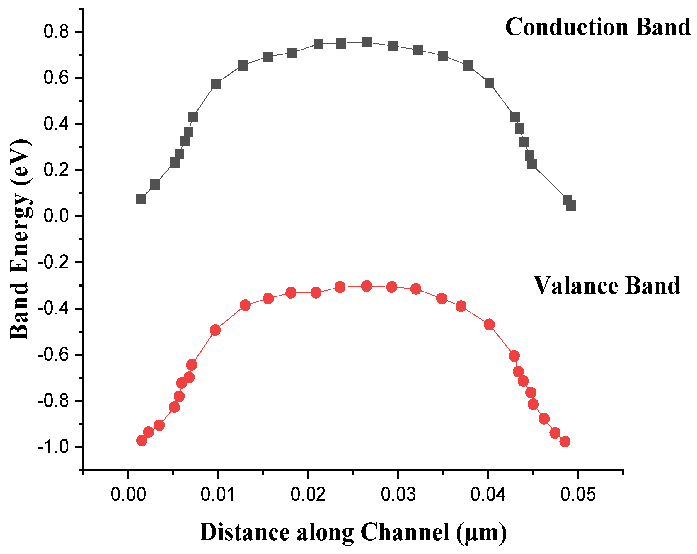
Figure 7 shows the electric potential distribution of 10 nm and 40 nm CGAA-JLFET. Variation of potential distribution in a 10 nm and 40 nm CGAA-JLFET is significant because of the difference in channel length, which subsequently leads to short channel effects. Since the DIBL and the reduced electrostatic control of the gate peak at the source and drain region, the potential profile exhibits a steep voltage gradient for the 10 nm channel. Due to the reduced size of the channel, control over the channel becomes difficult, reflected through the potential near the channel center trying to flatten. However, the device retains stronger gate electrostatic control at 40 nm, and potential distribution is more uniform across the channel with smoother variation from source to drain. The longer channel improves device performance and reduces SCEs by facilitating a more gradual change in potential. In both cases, the CGAA-JLFET structure yields better control on the channel than conventional planar transistors, but the 10 nm device is plagued by increased leakage currents and more severe potential fluctuations at higher drain voltages [
25].
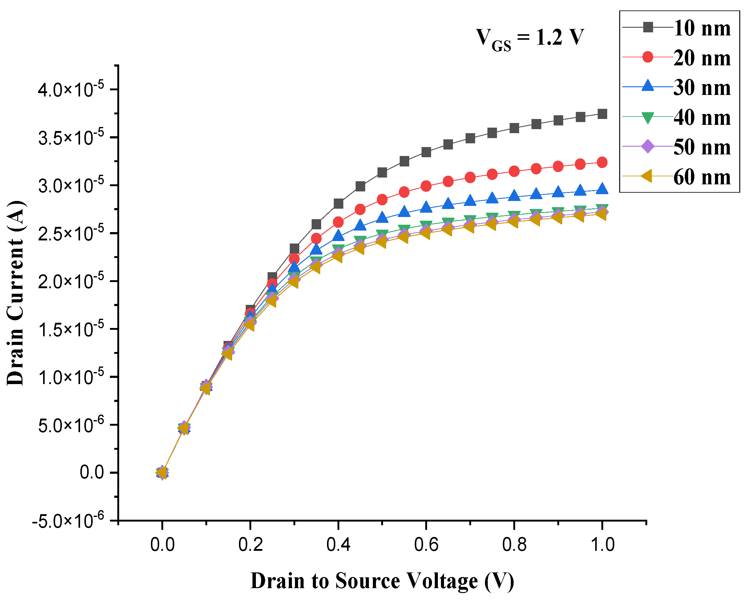
Figure 8 illustrates the I
D-V
DS characteristics of the CGAA-JLFET at V
GS = 1.2 V, with V
DS ranges from 0 to 1 V for different channel lengths. This device demonstrates a high ON-state current and a low OFF-state current, showcasing excellent electrostatic control, with a maximum drain current of 3.74606 × 10
-5 (at 10 nm), 3.23924 × 10
-5 (at 20 nm), 2.95 × 10
-5 A (at 30 nm), 2.76015 × 10
-5 (at 40 nm), 2.720923 × 10
-5 (at 50 nm) and 2.698054 × 10
-5 (at 60 nm) and saturation slope is about to 6.43265×10
-6 (at 10 nm), 4.07531 × 10
-6 (at 20 nm), 3.1868 × 10
-6 (at 30 nm), 3.15754 × 10
-6 (at 40 nm), 3.10029 × 10
-6 (50 nm) and 3.05913 × 10
-6 (at 60 nm). It can be understood here that the maximum drain current and saturation slope increase as channel length decreases. As the technology scales down during different nodes (10, 20, 30, 40, 50, and 60 nm), the output characteristics of the silicon-based CGAA-JLFET follow key trends. With smaller nodes (10-30 nm), electrostatic control improves, short channel effects are reduced, and the subthreshold slope steepens, leading to higher current drivability and lower leakage. On the other hand, larger nodes (40–60 nm) suffer from more severe short channel effects, such as threshold voltage roll-off and higher leakage currents, resulting in reduced performance efficiency. The drain current is proportional to the gate voltage, and the devices have typical saturation behavior, with smaller nodes controlling these effects better.
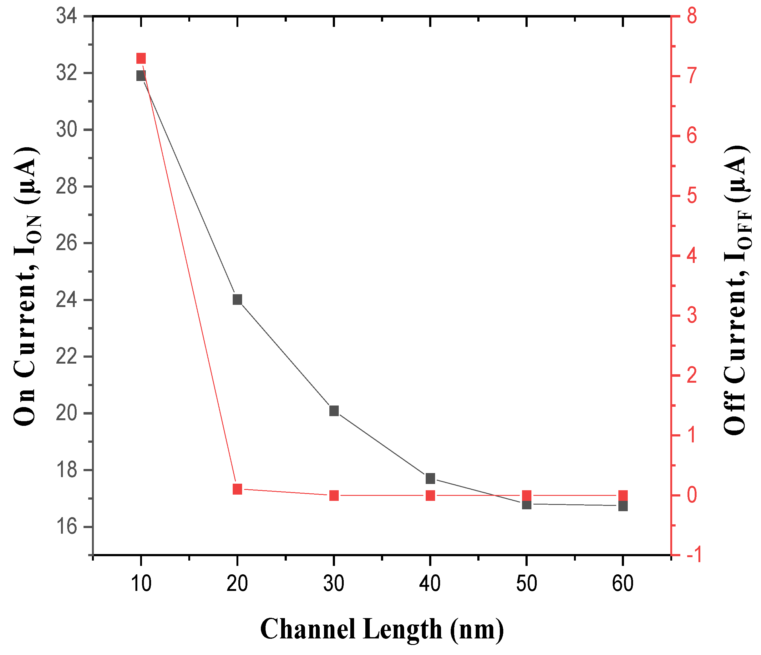
Figure 9 illustrates the on-current and off-current variations of Si-based CGAA-JLFET with different channel lengths [
26]. Mathematical expressions for subthreshold slope (SS) and drain-induced barrier lowering (DIBL) are explained in Equations 2 and Equation 3, respectively:
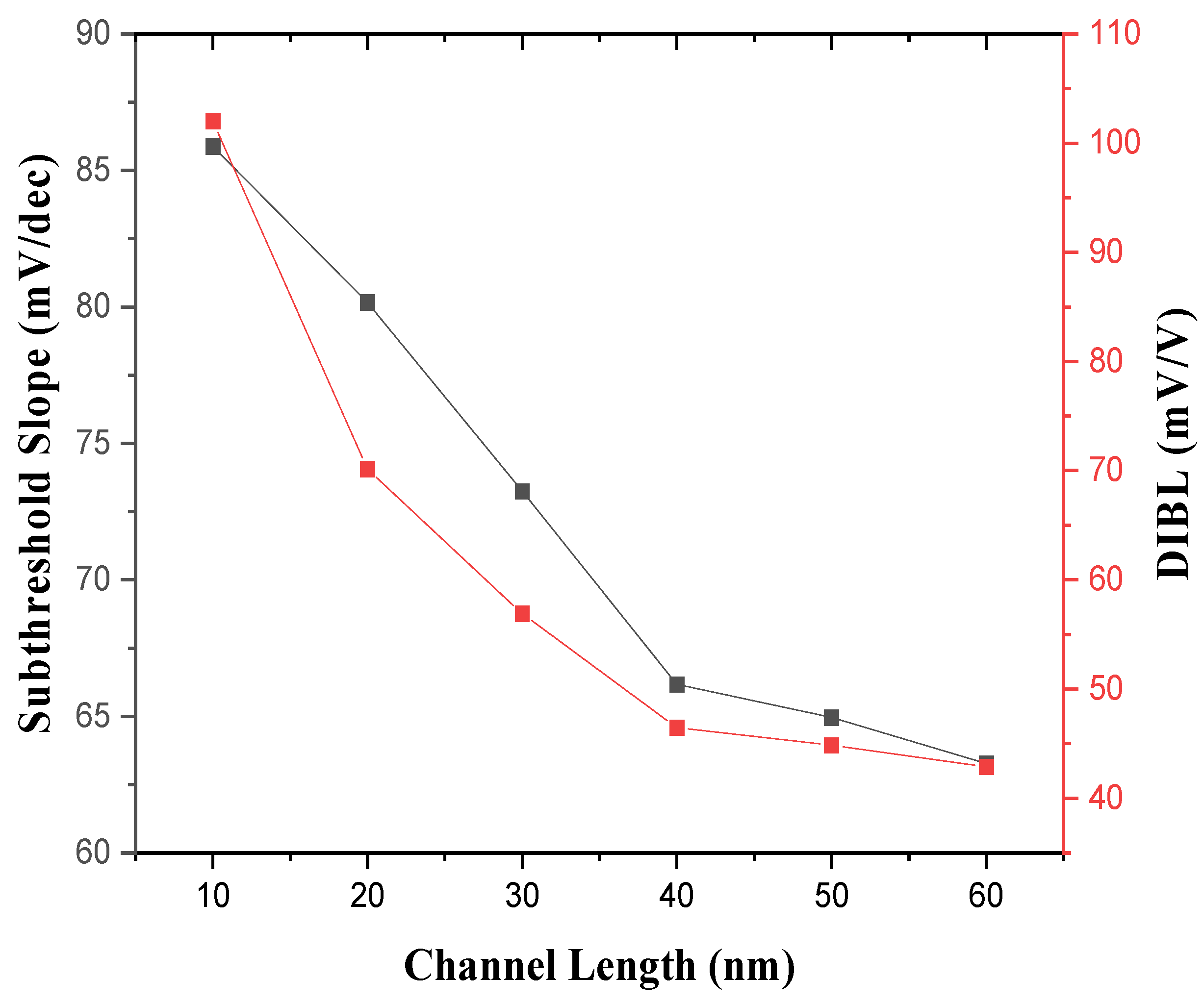
The simulated results for DIBL and SS versus different channel lengths are plotted in
Figure 10. We present distinct trends in the SS and DIBL as the technology node shrinks for silicon-based CGAA-JLFET. Due to the improved electrostatic control, the SS becomes steeper, typically close to the ideal 60 mV dec for larger nodes (40∼60 nm), and DIBL decreases, resulting in milder SCEs. However, smaller nodes (10∼30 nm) suffer from larger DIBL and shallower SS due to greater SCEs, resulting in more threshold voltage shifts and lower gate control. As a result, larger nodes (40 to 60 nm) provide better subthreshold performance and DIBL, resulting in less electric loss. When channels have extensive lengths, gate electrostatic control effectively seals leakage currents. When channels get shorter, the gate loses its capacity to entirely regulate current, resulting in greater leakage in off-state mode [
27].
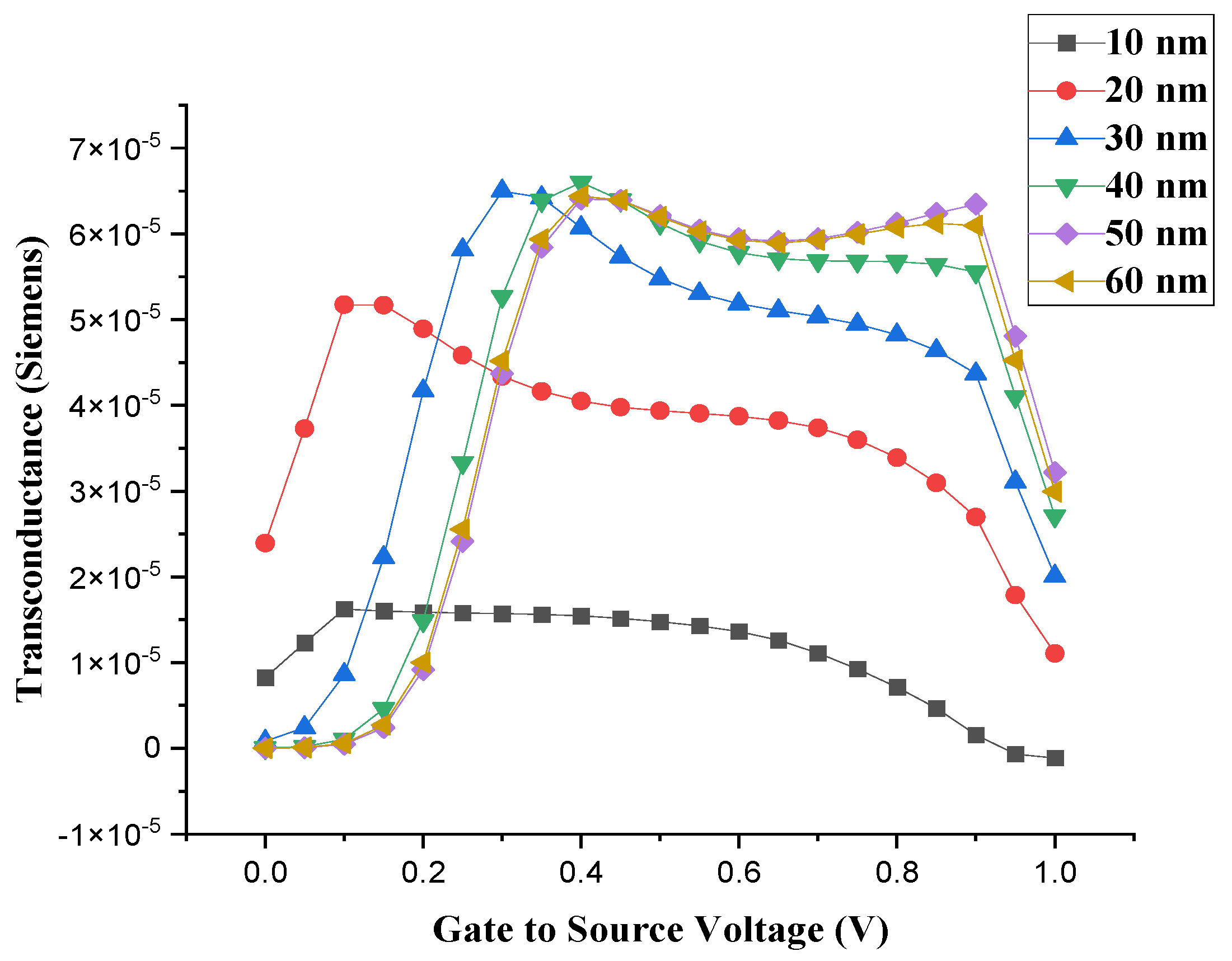
Figure 11 illustrates the channel length dependency of the Si-based CGAA-JLFET transconductance for different channel lengths ranging from 10 nm to 60 nm. As the technology node scales down, the transconductance of silicon-based CGAA-JLFET has been improved. For larger nodes (40-60 nm), higher transconductance is achieved because of enhanced electrostatic control and reduced SCEs, thereby enabling better current modulation as a function of gate voltage. However, smaller nodes (10–30 nm) exhibit more pronounced SCEs, resulting in lower transconductance and less efficient control over the channel current. Larger nodes exhibit higher transconductance because of better gate control and less leakage, and they are suitable for higher-end applications [
28].
5. Comparative DC Analysis of Si-Based ` CGAA-JLFET with Different Channel Lengths
The analysis of CGAA-JLFET studies with varying channel lengths is presented in this study.
Table 4 compares the proposed architectures with gate lengths between 10 and 60 nm in terms of DIBL, on and off current, saturation slope, subthreshold slope, maximum drain current, threshold voltage, and gate length. This study demonstrates that the subthreshold slope of CGAA-JLFET with channel lengths of 40, 50, and 60 nm is remarkably close to the ideal value of 60 mV/V, at roughly 66 mV/V, 64 mV/V, and 63 mV/V, respectively. Finally, we have compared the performance of Si-based CGAA-JLFET with those accessible architectures in the literature in
Table 5.
6. AC Analysis of Si-Based CGAA-JLFET with Different Channel Lengths
As for semiconductor devices, the channel length of a CGAA-JLFET greatly affects its performance. Since high-speed, low-power devices are in high demand, their behavior as channel length changes should be studied. In this study, the AC analysis is done on a CGAA-JLFET with channel length variation from 10 nm to 60 nm. The main purpose is to analyze their change in transconductance, output conductance, the unity gain cut-off frequency, and capacitance when the channel length changes. We explore these relationships to obtain deeper insights into the trade-offs between high-frequency performance, power efficiency, and device scalability. This analysis of the scaling-based enhancement of the characteristics of CGAA-JLFET aids in the design of CGAA-JLFET for applications ranging from high-speed devices to low-power devices, and essentially, a more thorough understanding of the effects of scaling in nanoelectronics can be achieved.
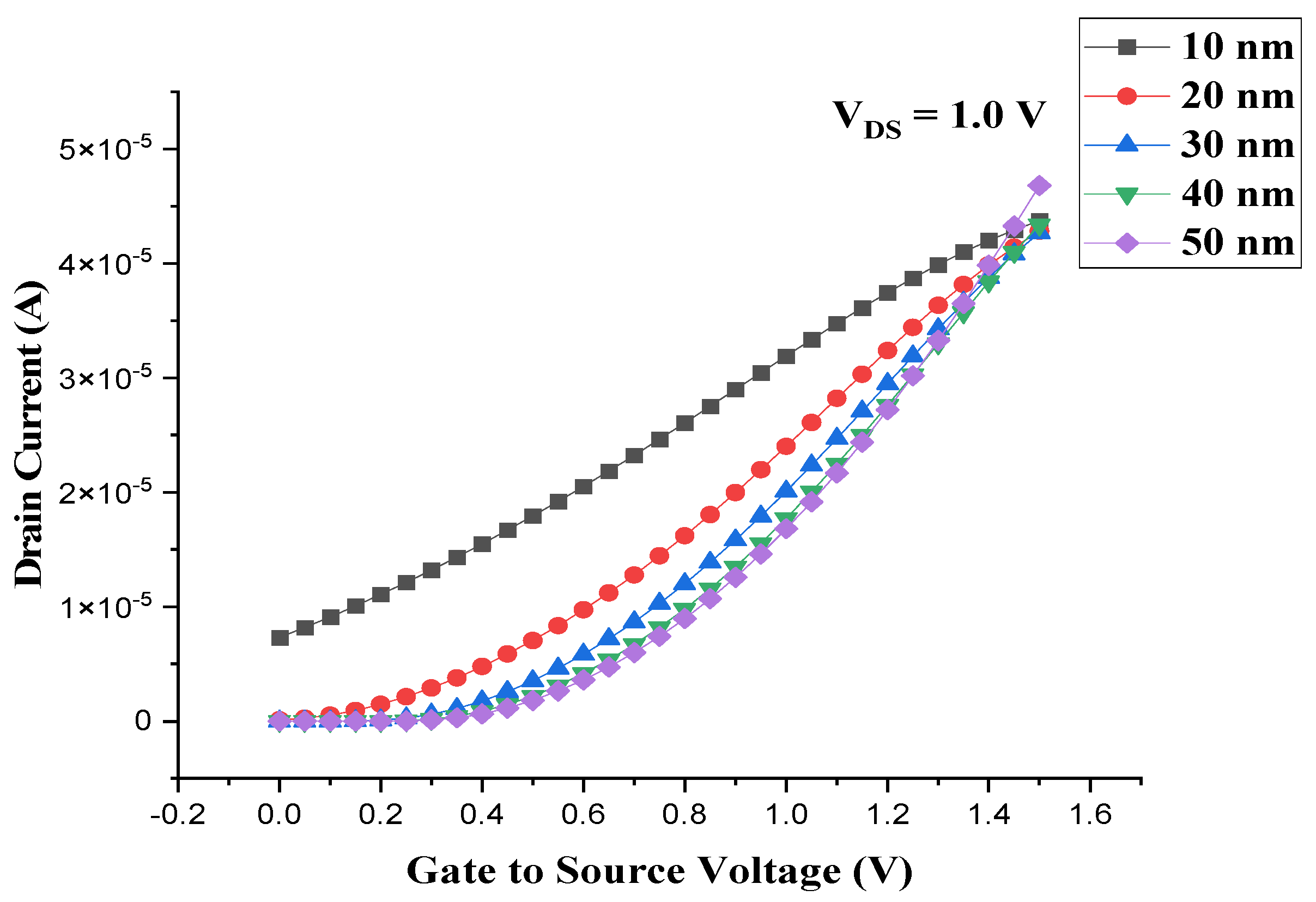
Figure 12 presents the simulated transfer characteristics of CGAA-JLFET for AC analysis at different channel lengths ranging from 10 nm to 60 nm. These I
D-V
GS characteristics of the CGAA-JLFET have been plotted at V
DS = 1.0 V, spanning a range of V
GS from 0 to 1.5 V with 10
9 Hz frequency.
Figure 13 shows transconductance variation against gate voltage with different channel lengths of CGAA-JLFET. The combined results of
Figure 12 and
Figure 13 have been compiled in
Table 6.
Table 6 shows the maximum drain current, maximum transconductance, and maximum oscillation frequency of a CGAA-JLFET with different channel lengths (10 nm, 20 nm, 30 nm, 40 nm, and 50 nm). Further data on how the channel length affects the transistor performance, conducting current, switching efficiently, and operating at high frequency are needed. It is obvious from
Table 6 that the maximum drain current slightly reduces as the channel length increases from the
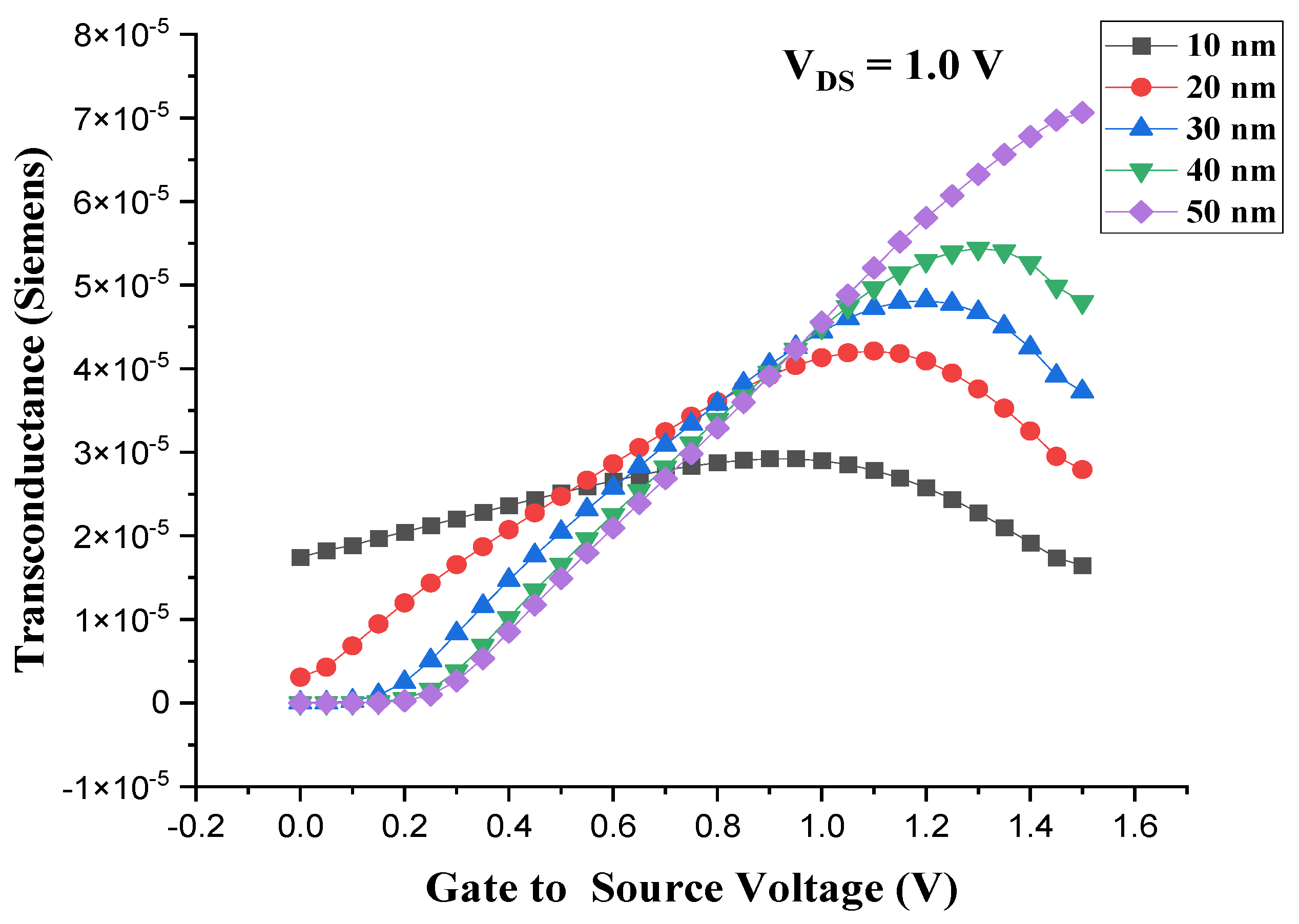
Table 6. For example, at 10 nm, the maximum drain current is 4.37285 × 10⁻⁵ A, and at 50 nm, it reduces to 4.20062 × 10⁻⁵ A. It aligns with FETs' well-known behavior, as longer channels result in a less efficient current passage because of increased resistance and parasitic effects. When the channel length increases, the effective gate control of the channel is less, and it is hard to drive current through the device. The trend in the maximum transconductance is also similar. The transconductance obtained is 2.92304 × 10⁻⁵ Siemens at 10 nm; however, the channel length harms the transconductance. At maximum, for 50 nm, it provides the transconductance value in the order of 7.06235 × 10⁻⁵ Siemens. Because the gate voltage controls the drain current less effectively, the device's transconductance decreases as the channel length increases. The channel length also decreases the maximum oscillation frequency. Finally, we obtained the maximum oscillation frequency of 1969.02945 GHz at 10 nm, which decreases as we move down to 50 nm, where the frequency becomes 477.220384 GHz.
Therefore, based on the above discussion, it has again shown that higher channel lengths lead to poorer device switching speeds, which further reduces the maximum oscillation frequency of the device, while lower channel lengths result in higher cut-off frequencies, which allow it to be run at higher speeds. From the data in
Table 6, we can conclude that this data agrees with the finding of the plot and previous analysis that shorter channel lengths (e.g., 10 nm) exhibit better high-frequency performance, higher transconductance, and larger drain currents, which is why these are good for switching speeds. On the other hand, the longer channel lengths (e.g., 50 nm) are more stable and have lower leakage and parasitic effects than shorter lengths, but they also run at lower frequencies and have reduced current driving capabilities. They show the importance of choosing an appropriate channel length and the trade-off between speed, power, and stability for the specific application.
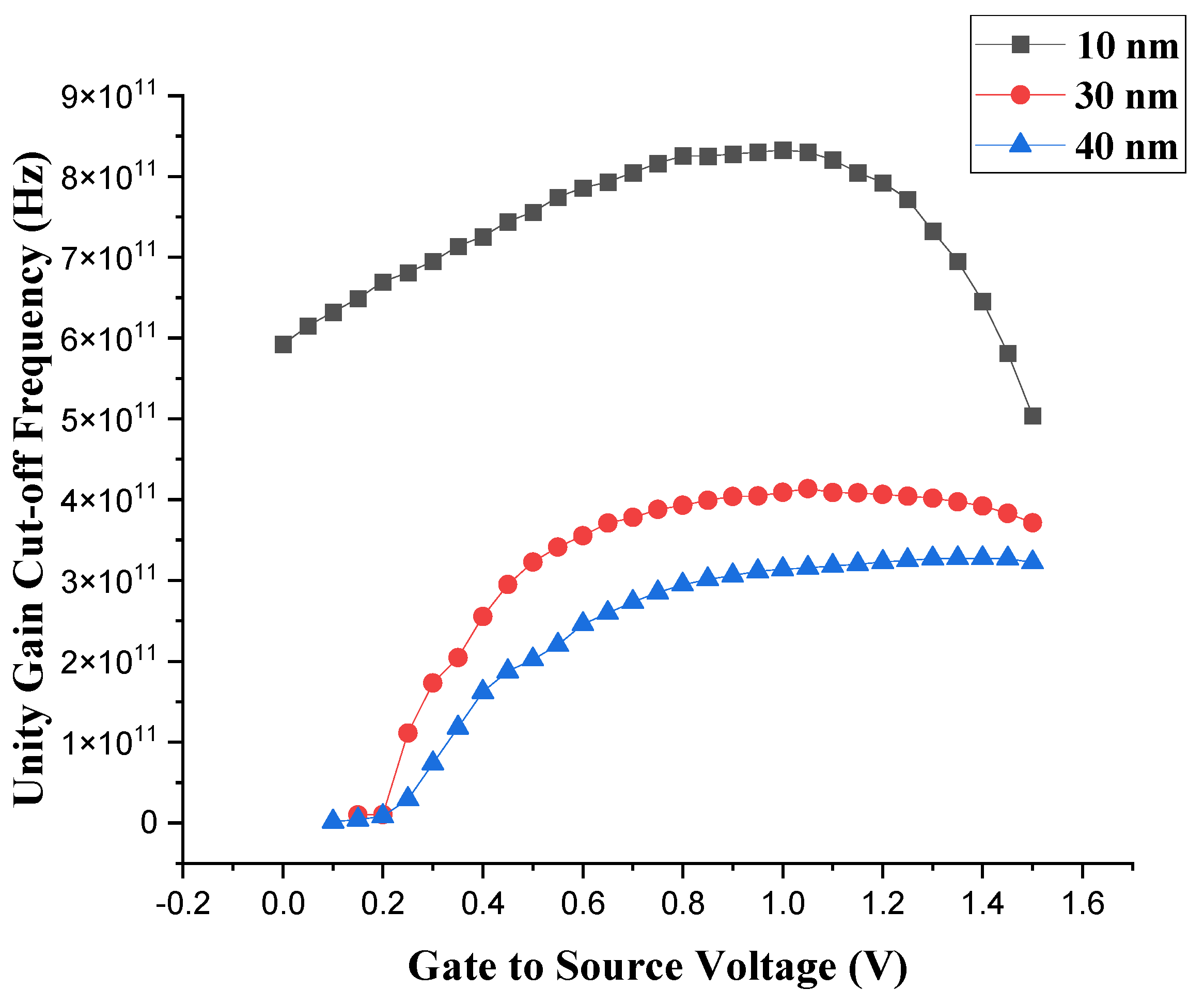
Figure 14 illustrates how the unity gain cut-off frequency depends on the gate-to-source voltage of a CGAA-JLFET with different channel lengths of 10 nm, 30 nm, and 40 nm. It shows that the cut-off frequency as a function of gate-to-source voltage reveals the effect of channel length on the device's high-frequency performance. Cut-off frequency, f
T, can be expressed in Equation 4, where g
m is transconductance, and C
gg is output capacitance:
As such, from
Figure 14, it is clear that the 10 nm channel length exhibits the highest unity gain cut-off frequency of all gate voltages, with the voltage rising from 0 to approximately 1.5 V. This implies that the switch time is faster with reduced SCEs of transistors and the shorter channel length provides better gate control due to enhanced field penetration with effective change in work function. At smaller dimensions, the influence of the gate controls the channel's conductivity and improves its operating frequencies. Although a shorter channel length improves performance faster, it may also bring extra leakage currents and probably threshold voltage roll-off that may affect long-term operating transistors in its practical applications. However, the unity gain cut-off frequency decreases as the channel length increases to 30 and 40 nm. That is likely due to increased parasitic capacitances from the larger physical dimensions of the channel. Besides this, longer channel lengths result in stronger SCEs that result in less gate control over the channel, lowering the device's capability of switching at high frequencies. Although the 10 nm transistor has a reduced cut-off frequency, the 30 nm and 40 nm transistors have a reduced cut-off frequency. The devices are less prone to leakages and provide closer to comparable dynamic stability as the 10 nm transistor, especially for higher gate voltages.
Experimental results show that the CGAA-JLFET for 10 nm, 30 nm, and 40 nm follow the same voltage dependency curve, and the unity gain cut-off frequency increases as the gate-to-source voltage increases. The channel conductivity is improved as the gate voltage increases, giving the device the potential to function at higher frequencies. However, the cut-off frequency increases, but only up to a certain gate voltage threshold, after which it becomes saturated, indicating a transition into saturation mode where the variation in drain current concerning gate voltage is not substantial.
Figure 14, on the whole, shows the trade-offs between channel length and high-frequency performance. However, shorter channels like the 10 nm device have better performance concerning speed and frequency response but come with problems like leakage current and problems of SCEs. The 30 nm and 40 nm channels appear to scale better to longer channels where slower switching speeds, as compared to the 10 nm and 20 nm channels, may be acceptable because of the greater power efficiency and stability [
33,
34,
35].
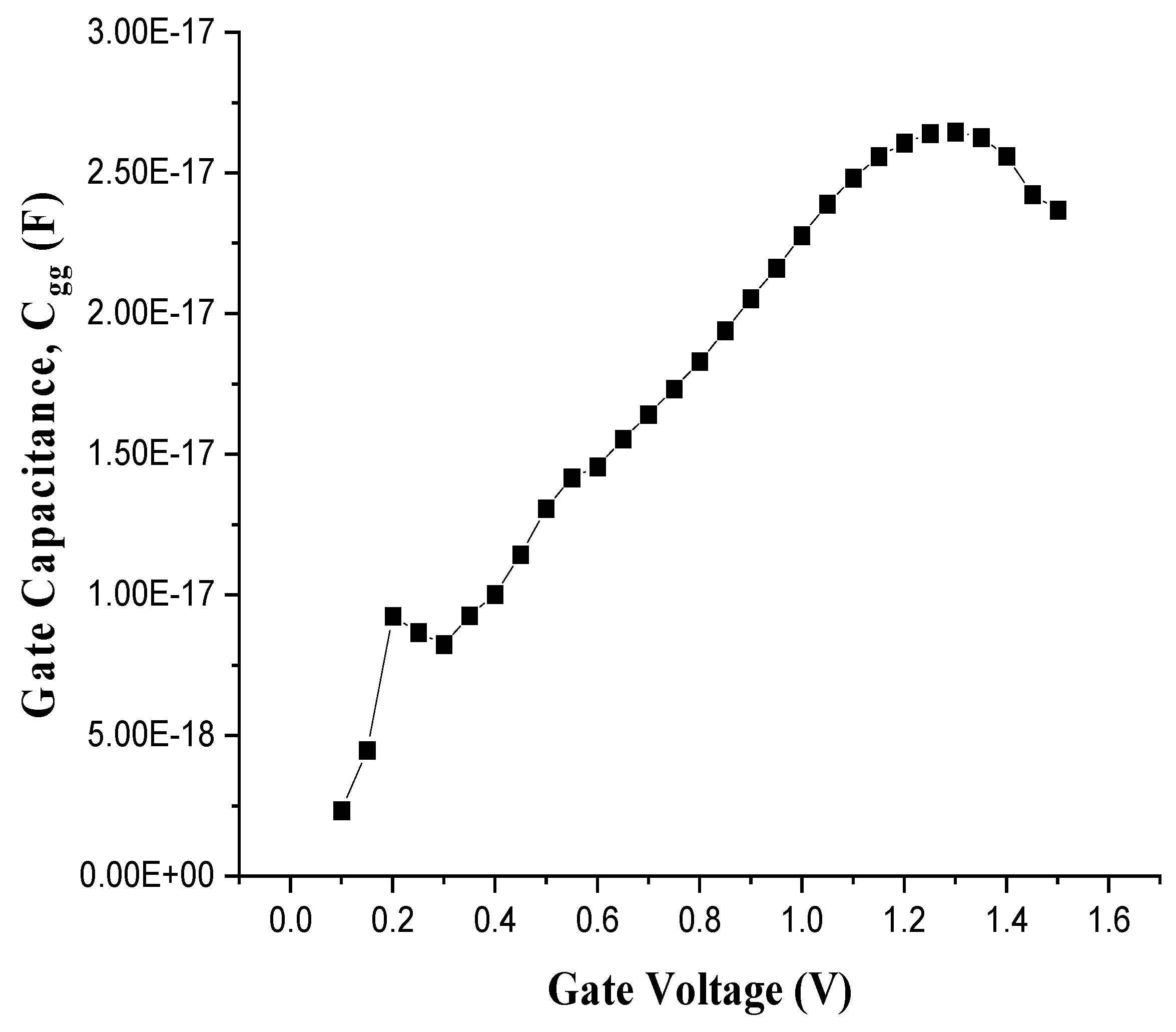
Figure 14 illustrates gate capacitive variation against gate voltage for 40 nm CGAA-JLFET. In CGAA-JLFET, gate capacitance (C
gg) or gate-to-channel capacitance is one of the important parameters. The capacitance between the transistor's gate and channel region is important in determining the device frequency response, switching speed, and other parameters. In CGAA-JLFET, C
gg depends on the 2D gate geometry, and the cylindrical gate enables stronger channel electrostatic control than in the planar devices. As channel length decreases, the gate capacitance increases since the gap between the gate and channel can be decreased. That makes the device better at controlling the current flow. While this increase in gate capacitance can cause higher parasitic delays, the resulting higher parasitic delays can be an issue for the transistor's high-frequency performance. Since C
gg directly affects transistor transconductance, cut-off frequency, and dynamic behavior in AC analysis, it is important to understand C
gg in AC analysis and to become as small as possible, which helps in having minimum capacitive delay in high-speed applications.
7. Simulated Results and Discussion for GaAs-Based JLFET
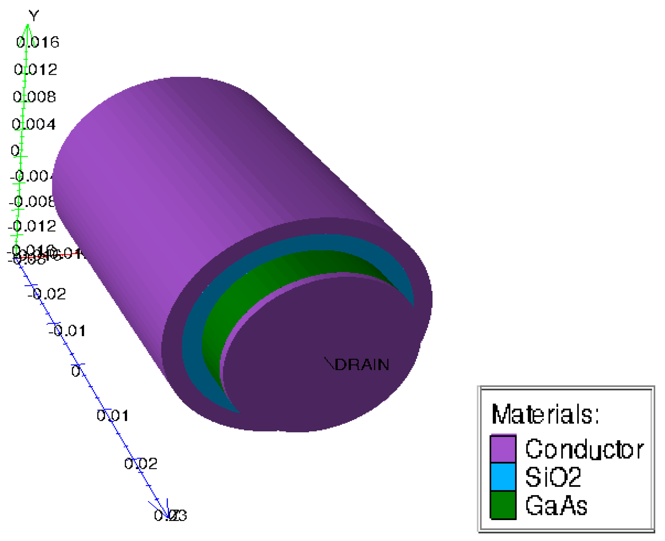
Materials that contain group III elements (such as aluminum, gallium, and indium) and group V elements (such as nitrogen, phosphorus, arsenic, and antimony) of the periodic table are referred to as group III-V materials. This material combination has a direct energy band gap and unique electrical and optoelectronic characteristics. A comprehensive investigation of a three-dimensional JLFET with a cylindrical gate-all-around architecture has also been performed using GaAs, III-V material. The channel material used to construct the device construction shown in
Figure 16 is GaAs. The device gate length is 40 nm, and the radius is 14 nm. The Silvaco ATLAS tool is utilized in this simulation. The Shockley-Read-Hall and AUGER recombination models analyzed the recombination effects at high current densities. Equations with linked and decoupled forms were modified to integrate the NEWTON and GUMMEL models. The electrical properties of a novel transistor CGAA-JLFET with an all-around gate layout are simulated in this paper. The recommended device parameters are listed in
Table 7, and the different properties of silicon and GaAs are discussed in
Table 8.
Modern semiconductor technology values CGAA-JLFET for their simple structure design that does away with p-n junctions, thus making them optimal for low-power and high-frequency applications. A simple device structure reduces cost while improving reliability and optimizing current transmission in CGAA-JLFET. High-speed and high-frequency applications demonstrate better performance from GaAs-based CGAA-JLFET over Si-based CGAA-JLFET because GaAs offer superior electron mobility, higher drift velocity, and reduced leakage currents.
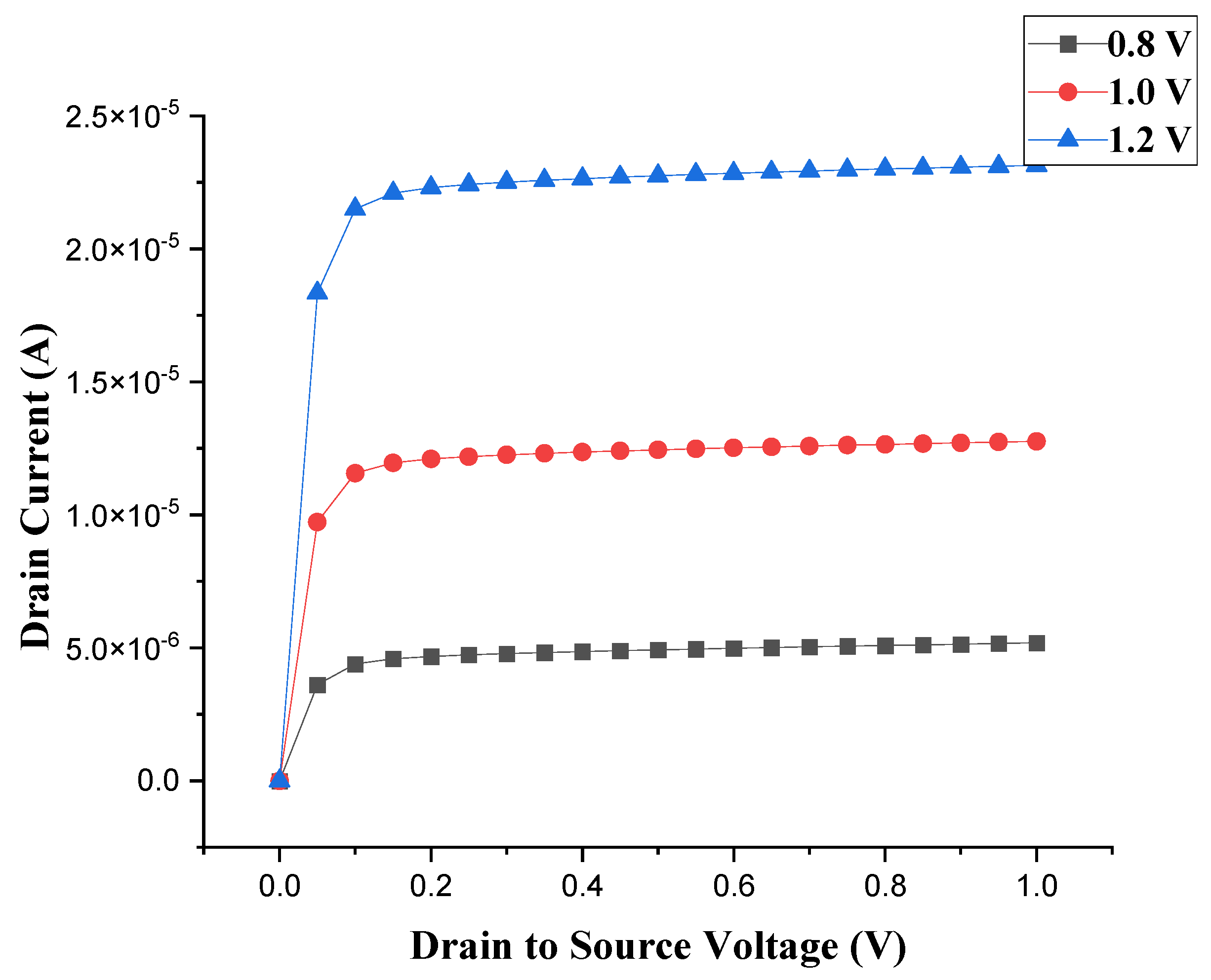
Figure 17 illustrates the 40 nm GaAs-based CGAA-JLFET output characteristics at various VGS = 0.8 V, 1.0 V, and 1.2 V, with V
DS ranges from 0 to 1 V. The output curve of the GaAs part shows significant saturation at a higher current level than the corresponding curve being developed here but at higher drain voltages. In GaAs-based CGAA-JLFET, GaAs's higher electron mobility leads to a much sharper increase in current with increasing drain voltage. It improves current drive and switching behavior. Due to GaAs's superior material properties, the output curve has generally higher saturation currents at a given drain voltage, particularly at smaller channel lengths. However, for the silicon-based CGAA-JLFET, the output characteristics generally show that the output current gradually increases as the drain voltage increases. Due to slower electron mobility in silicon, the current drive capability is usually lower.
Figure 18 presents the simulated transfer characteristics of 40 nm GaAs-based CGAA-JLFET and P+ Polysilicon, which have been used to fulfill the high gate work function requirement to achieve appropriate V
TH value. The transfer characteristics of GaAs-based CGAA-JLFET yield faster on-to-off-state transitions because GaAs exhibit higher electron mobility than silicon-based CGAA-JLFET. GaAs devices demonstrate lower subthreshold swing characteristics and rapid switching processes; thus, they can operate effectively with reduced gate voltage requirements. However, silicon-based CGAA-JLFET demonstrates slower behavior between on and off states because of the decreased mobility of carriers.
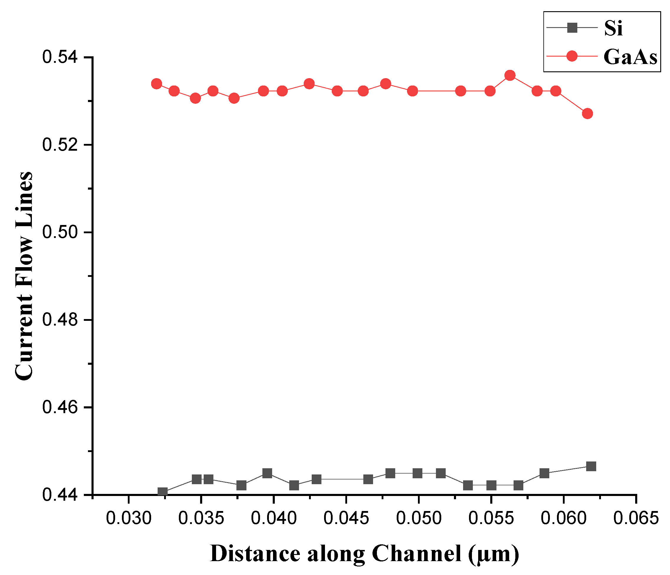
The current flow lines of a 40 nm CGAA-JLFET made of silicon and a 40 nm CGAA-JLFET made of GaAs are depicted in
Figure 19. The current flow lines of 0.45 for silicon and 0.53 for GaAs-based JLFET are shown in
Figure 18. Both drift and diffusion phenomena affect current in silicon-based CGAA-JLFET, and because of the indirect energy band gap, current flow lines are directly driven by the voltages. Like silicon, drift and diffusion phenomena affect current in GaAs-based JLFET. However, GaAs has a direct energy band gap, meaning current flow lines are more concentrated and less dispersed than in silicon.
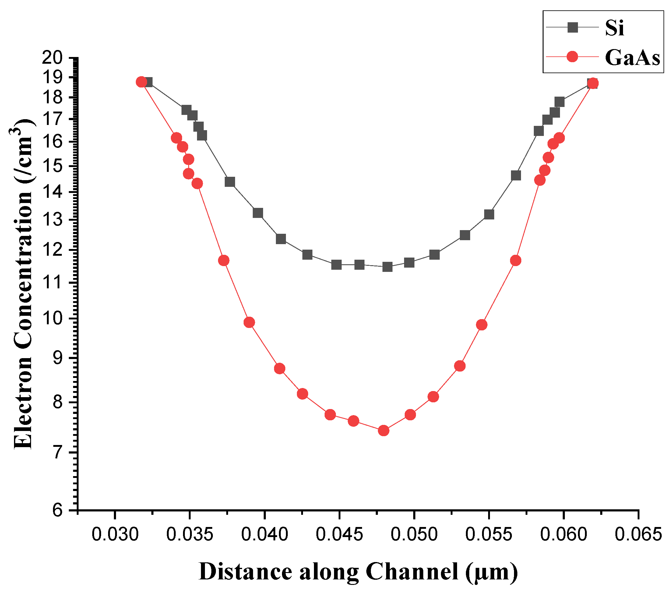
The electron concentration of a 40 nm CGAA-JLFET made of silicon and a 40 nm CGAA-JLFET made of GaAs is displayed in
Figure 20. Understanding the carrier density or electron concentration is essential to comprehending any device's electrical operation. Temperature, inherent properties, and doping can also have an impact. The highest electron concentration, up to 10
19 cm
-3, for both silicon and GaAs-based CGAA-JLFET is displayed in
Figure 20. Compared to silicon CGAA-JLFET, GaAs-based CGAA-JLFET has deeper and greater electron concentrations [
36,
37,
38].
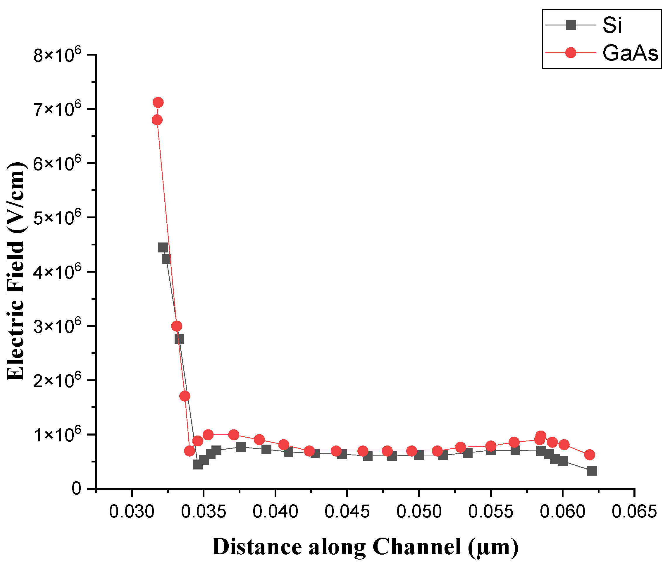
Figure 21 shows the electric fields of 40 nm silicon and GaAs-based JLFET. A key element in evaluating the performance of any device is the electric field distribution, which is impacted by the material properties, doping profiles, and device structure. However, increased current mobility in GaAs-based JLFET results in more concentrated and distinct electric field lines. The GaAs JLFET's electric field distribution is less diffused and more concentrated around the gate region, allowing it to control the conduction process more precisely. Due to wide bandgaps and high mobility of GaAs, GaAs-based devices use better electrostatic control, higher drive currents, and quicker electron transport than silicon devices [
39,
40].
Table 9 shows the performance comparison of 40 nm GaAs and silicon-based CGAA-JLFET with different parameters. For the most part, GaAs-based CGAA-JLFET has better output and transfer characteristics, subthreshold swing (SS), and DIBL than silicon-based CGAA-JLFET owing to the higher electron mobility and improved material properties of GaAs. GaAs-based devices are faster-switching devices, have a smaller subthreshold swing, and lower leakage currents, and consequently, they are suitable for high-speed and low-power applications. However, performance limiting issues such as higher leakage current, slower switching characteristics, and higher DIBL resulting in limited performance in some of the advanced, miniaturized applications are encountered with the silicon-based CGAA-JLFET, which, although are cost-effective and easy to integrate with the existing CMOS technologies.
The CGAA-JLFET exhibits important advantages such as low power and high-frequency operation, and channel length is one of the key parameters to enhance performance. GaAs-based CGAA-JLFET outperforms silicon-based CGAA-JLFET consistently as the channel length reduces from 60 nm to 10 nm owing to the higher electron mobility, lower leakage currents, and higher speed of switching of the former, making GaAs-based CGAA-JLFET favorable for high frequency and low power operation. However, GaAs have the highest power efficiency and speed at channel lengths (10 nm to 30 nm) compared to Si-based JLTs because of leakage and slow switching in the latter. Increasing the channel length (40 nm to 60 nm) to Si-based CGAA-JLFET makes better sense in low-cost and low-power devices, while GaAs continue to lead on high-speed and high-frequency operations. Therefore, GaAs are used for high-performance, low-power devices because of their inherent small electron mobility, while silicon is used for general-purpose devices.
8. Conclusion
Therefore, in summary, CGAA-JLFET is a major step forward in semiconductor technology due to the elimination of the conventional p-n junctions, which helps to reduce the number of device layers and improve the device performance. The reduced complexity of CGAA-JLFET is the key advantage because it results in lower fabrication costs and higher reliability. GaAs-based CGAA-JLFETs are advantageous over silicon-based CGAA-JLFETs due to their higher electron mobility, higher drift velocity, and lower leakage currents, facilitating higher speed, higher frequency, and low power requirements. Si-based CGAA-JLFET has become more cost-attractive and more easily integrated into existing manufacturing processes, but GaAs-based CGAA-JLFET has greater performance requirements for niche applications where higher efficiency and faster switching are required. Finally, choosing between silicon and GaAs junctionless transistors depends on the application, cost, speed, or power consumption. The characteristics of the two materials make them suited to different purposes, but GaAs hold the most potential concerning future high-performance devices.
Author Contributions
Conceptualization, P.S.; methodology, P.S.; software, P.S.; validation, P.S., A.U. and S.Y.; formal analysis, P.S.; investigation, C.N.; resources, P.S.; data curation, P.S.; writing—original draft preparation, P.S., A.U., S.Y., C.N. and A.S.; writing—review and editing, P.S., A.U., S.Y., C.N. and A.S.; visualization, C.N.; supervision, A.S.. All authors have read and agreed to the published version of the manuscript.
Funding
This research received no external funding.
Data Availability Statement
The original contributions presented in this study are included in the article. Further inquiries can be directed to the corresponding author.
Acknowledgments
The author thanks the School of Physical Sciences, Banasthali Vidyapith, Rajasthan, India, and the Department of Mathematics, Institute of Science, Banaras Hindu University, U.P., India for helpful discussions and support of device fabrication simulation.
Conflicts of Interest
The authors declare no conflicts of interest.
Abbreviations
The following abbreviations are used in this manuscript:
| JLFET |
Juncionless field effect transistor |
| SCEs |
Short channel effects |
| DIBL |
Drain-induced barrier lowering |
| SS |
Subthreshold slope |
References
- Sze, S.; Ng, K. K. LEDs and lasers. Physics of semiconductor devices, 2006, vol. 3, pp. 601-657. [CrossRef]
- Jurczak, M.; Collaert, N.; Veloso, A.; Hoffmann, T; Biesemans, S. Review of FINFET technology. In IEEE international SOI conference, 2009, IEEE, pp. 1-4.
- Colinge, J. P. The junctionless transistor. In Emerging devices for low-power and high-performance nanosystems: Jenny Stanford Publishing, 2018, pp. 2-72.
- Theis, T. N.; Wong, H. S. P. The end of Moore's law: A new beginning for information technology. Computing in science & engineering, 2017, vol. 19, no. 2, pp. 41-50.
- Kumar, M. J.; Sahay, S. Junction-Less Field Effect Transistors: The First Transistor to be Conceptualized. 75th Anniversary of the transistor, pp. 51-63, 2023.
- Srivastava, S.; Acharya, A. Challenges and future scope of gate-all-around (GAA) transistors: Physical insights of device- circuit interactions. in Device Circuit Co-Design Issues in FETs: CRC Press, 2024, pp. 231-258.
- Baksh, S. S.; Sarin, R.; Amin, S. I.; Anand, S. Design of GaAs based Junctionless field effect transistor and its performance evaluation. Journal of Nanoelectronics and Optoelectronics, 2018, vol. 13, no. 1, pp. 32-37. [CrossRef]
- Frank, D. J.; Dennard, R. H.; Nowak, E.; Solomon, P. M.; Taur, Y.; Wong, H. S. P. Device scaling limits of Si MOSFETs and their application dependencies. Proceedings of the IEEE, vol. 89, no. 3, pp. 259-288, 2001. [CrossRef]
- Raut, P.; Nanda, U.; Panda, D. K. Recent trends on junction-less field effect transistors in terms of device topology, modeling, and application. ECS Journal of Solid State Science and Technology, 2023, vol. 12, no. 3, p. 031010. [CrossRef]
- Hossain, N. M.; Quader, S.; Siddik, A. B.; Chowdhury, M. I. B. TCAD based performance analysis of junctionless cylindrical double gate all around FET up to 5nm technology node. In 2017 20th International Conference of Computer and Information Technology (ICCIT), 2017: IEEE, pp. 1-4.
- Ghosh, S.; Jana, A.; Agnihotri, A. K.; Kundu, S.; Das, D.; Sarkar, S. K. DC and analog/RF performance comparison of renovated GAA JLFET structures. in 2022 IEEE VLSI Device Circuit and System (VLSI DCS), 2022: IEEE, pp. 80-84.
- Srivastava, P.; Upadhyaya, A.; Yadav, S.; Negi, C. Performance Evaluation of Junctionless Cylindrical Gate-All-Around FET for Low Power Applications. Semiconductor Science and Information Devices, 2023, vol. 5, no. 2, pp. 1-10,. [CrossRef]
- Kumari, A.; Saini, A.; Kumar, A.; Kumar, V.; Kumar, M. Recent Developments and Challenges in Strained Junctionless MOSFETs: A Review. in 2023 International Conference on Computational Intelligence and Sustainable Engineering Solutions (CISES), 2023: IEEE, pp. 118-122.
- Dixit, V. K.; Gupta, R.; Srinivas, P.; Dubey, S. Back Bias Induced Modeling of Subthreshold Characteristics of SOI Junctionless Field Effect Transistor (JLFET). Silicon, 2021. vol. 13, pp. 1961-1967. [CrossRef]
- DEHZANGI, A. FABRICATION AND SIMULATION OF P-TYPE JUNCTIONLESS SILICON NANO-WIRE TRANSISTOR ON SILICON ON INSULATOR BY AFM NANO LITHOGRAPHY. School of Graduate Studies, Universiti Putra Malaysia, 2012.
- Scognamiglio, L. 3D Junctionless-FET technology: A comparative TCAD simulation study with FinFET and NSGAAFET. Politecnico di Torino, 2022.
- Chuan, M. W. et al. A review of the top of the barrier nanotransistor models for semiconductor nanomaterials. Superlattices and Microstructures, 2020, vol. 140, p. 106429. [CrossRef]
- Xie, Q.; Xu, J.; Taur, Y. Review and critique of analytic models of MOSFET short-channel effects in subthreshold. IEEE transactions on electron devices, 2012, vol. 59, no. 6, pp. 1569-1579. [CrossRef]
- Rao, R.; Srivastava, A.; Blaauw, D.; Sylvester, D. Statistical analysis of subthreshold leakage current for VLSI circuits. IEEE Transactions on Very Large Scale Integration (VLSI) Systems, 2004, vol. 12, no. 2, pp. 131-139. [CrossRef]
- Querlioz, D. et al. On the ability of the particle Monte Carlo technique to include quantum effects in nano-MOSFET simulation. IEEE transactions on electron devices, 2007, vol. 54, no. 9, pp. 2232-2242. [CrossRef]
- Colinge, J. P. et al. Nano-wire transistors without junctions. Nature nanotechnology, 2010, vol. 5, no. 3, pp. 225-229.
- Misra, S.; Biswal, S. M.; Bara, B.; Swain, S. K.; Pati, S. K. Study of effect of downscaling on the analog/RF performance of gate all around JLMOSFET. in 2018 IEEE Electron Devices Kolkata Conference (EDKCON), 2018: IEEE, pp. 234-241.
- Chen, L.C. et al. The physical analysis on electrical junction of junctionless FET. AIP Advances, 2017, vol. 7, no. 2. [CrossRef]
- Singh, B.; Gola, D.; Singh, K.; Goel, E.; Kumar, S.; Jit, S. Analytical modeling of subthreshold characteristics of ion-implanted symmetric double gate junctionless field effect transistors. Materials science in semiconductor processing, 2017, vol. 58, pp. 82-88. [CrossRef]
- Meriga, C.; Ponnuri, R. T.; Krishna, B. V.; Saidulu, S. A.; Prakesh, M. D. Dual gate junctionless gate-all-around (JL-GAA) FETs using hybrid structured channels. In 2020 International Conference for Emerging Technology (INCET), 2020: IEEE, pp. 1-4.
- Pandey, S.; Sahu, C.; Singh, J. A highly linear RF mixer using gate-all-around junctionless transistor. International Journal of Electronics Letters, 2017, vol. 5, no. 2, pp. 129-136.
- Singh, B. Analytical Modeling and Simulation of Double Gate Junctionless Field Effect Transistors (DG-JLFETs). 2017.
- Hossain, S.; Iqbal, M. A.; Samant, P.; Siddiki, M. K.; Rahman, M. More Than a Device: Function Implementation in a Multi-Gate Junctionless FET Structure. Journal of Electronics and Electrical Engineering, 2023, pp. 1–11-1–11.
- Pavanello, M. A.; Martino, J. A. A.; Simoen, E.; Rooyackers, R.; Collaert, N.; Claeys, C. Temperature influences on FinFETs with undoped body. ECS Transactions, 2007, vol. 6, no. 4, p. 211. [CrossRef]
- Nazarov, A.; Balestra, F.; Kilchytska, V.; Flandre, D. Functional nanomaterials and devices for electronics, sensors and energy harvesting. Springer, 2014.
- Yadav S.; Negi, C. M. S. Novel L-shaped drain dual-gate SiGe MOSFET for high-frequency, low power applications. International Journal of Numerical Modelling: Electronic Networks, Devices and Fields, 2023, vol. 36, no. 1, p. e3039.
- Kamath, A. et al. Junctionless CMOS transistors with independent doublegates. International Journal of Information and Electronics Engineering, 2013, vol. 3, no. 1, p. 13.
- Rewari, S.; Nath, V.; Haldar, S.; Deswal, S.; Gupta, R. AC analysis of Junctionless Double Surrounding Gate (JLDSG) MOSFET for Tera Hertz applications. in 2016 International Conference on Computational Techniques in Information and Communication Technologies (ICCTICT), 2016: IEEE, pp. 113-117.
- Joshi, R. K.; Arjun, T.; Ahish, S.; Sharma, D.; Vasantha, M.; Kumar, Y. Implementation of double-gate junctionless transistor and its circuit performance analysis. In 2016 IEEE Students' Technology Symposium (TechSym), 2016: IEEE, pp. 278-283.
- Sahu C.; Singh, J. Device and circuit performance analysis of double gate junctionless transistors at L g= 18 nm. The Journal of Engineering, 2014, vol. 2014, no. 3, pp. 105-110.
- Yarlagadda, N.; Verma, Y. K.; Amarnath, G. A temperature dependent drain current model of P+ SiC GAA JLFETs for enhanced analog/RF performance. Micro and Nanostructures, 2024, vol. 188, p. 207786. [CrossRef]
- Dharmender; Nigam, K.; Kumar, S. Performance assessment of cavity on source dual material split gate GaAs/InAs/Ge junctionless TFET for label-free detection of biomolecules. Applied Physics A, 2022, vol. 128, no. 10, p. 943.
- CONGER, J.; PECZALSKI, A.; SHUR, M. S. Temperature modeling of GaAs DCFL. International Journal of High Speed Electronics and Systems, 1992, vol. 3, no. 02, pp. 171-199.
- Zhang, C.; Li, X. III–V nano-wire transistors for low-power logic applications: a review and outlook. IEEE Transactions on Electron Devices, 2015, vol. 63, no. 1, pp. 223-234.
- Nowbahari, A.; Roy, A.; Marchetti, L. Junctionless transistors: State-of-the-art. Electronics, 2020, vol. 9, no. 7, p. 1174. [CrossRef]
Figure 1.
20 nm CGAA-JLFET structure with a solid view.
Figure 1.
20 nm CGAA-JLFET structure with a solid view.
Figure 2.
Transfer characteristics of Si-based CGAA-JLFET with different channel lengths.
Figure 2.
Transfer characteristics of Si-based CGAA-JLFET with different channel lengths.
Figure 3.
Threshold Voltage variations of Si-based CGAA-JLFET with different channel lengths.
Figure 3.
Threshold Voltage variations of Si-based CGAA-JLFET with different channel lengths.
Figure 4.
Electric field distribution in 10 nm and 40 nm-based CGAA-JLFET.
Figure 4.
Electric field distribution in 10 nm and 40 nm-based CGAA-JLFET.
Figure 5.
Energy band diagram of 10 nm Si-based CGAA-JLFET.
Figure 5.
Energy band diagram of 10 nm Si-based CGAA-JLFET.
Figure 6.
Energy band diagram of 40 nm Si-based CGAA-JLFET.
Figure 6.
Energy band diagram of 40 nm Si-based CGAA-JLFET.
Figure 7.
Potential distribution of 10 nm and 40 nm Si-based CGAA-JLFET.
Figure 7.
Potential distribution of 10 nm and 40 nm Si-based CGAA-JLFET.
Figure 8.
Output characteristics of Si-based CGAA-JLFET.
Figure 8.
Output characteristics of Si-based CGAA-JLFET.
Figure 9.
On Current and Off Current variations of Si-based CGAA-JLFET with different channel lengths.
Figure 9.
On Current and Off Current variations of Si-based CGAA-JLFET with different channel lengths.
Figure 10.
SS and DIBL variations in Si-based CGAA-JLFET with different channel lengths.
Figure 10.
SS and DIBL variations in Si-based CGAA-JLFET with different channel lengths.
Figure 11.
Transconductance variations of Si-based JLFET with different channel lengths.
Figure 11.
Transconductance variations of Si-based JLFET with different channel lengths.
Figure 12.
Transfer Characteristics of CGAA-JLFET with different channel lengths in AC analysis.
Figure 12.
Transfer Characteristics of CGAA-JLFET with different channel lengths in AC analysis.
Figure 13.
Transconductance variation against gate voltage of CGAA-JLFET with different channel lengths in AC analysis.
Figure 13.
Transconductance variation against gate voltage of CGAA-JLFET with different channel lengths in AC analysis.
Figure 14.
Unity Gain Cut-off Frequency variation against Gate Voltage for CGAA-JLFET with different channel lengths.
Figure 14.
Unity Gain Cut-off Frequency variation against Gate Voltage for CGAA-JLFET with different channel lengths.
Figure 15.
Gate Capacitance variation against Gate Voltage for 40 nm CGAA-JLFET.
Figure 15.
Gate Capacitance variation against Gate Voltage for 40 nm CGAA-JLFET.
Figure 16.
40 nm CGAA-JLFET structure with GaAs material.
Figure 16.
40 nm CGAA-JLFET structure with GaAs material.
Figure 17.
Output characteristics of 40 nm GaAs-based CGAA-JLFET.
Figure 17.
Output characteristics of 40 nm GaAs-based CGAA-JLFET.
Figure 18.
Transfer characteristics of 40 nm GaAs-based CGAA-JLFET.
Figure 18.
Transfer characteristics of 40 nm GaAs-based CGAA-JLFET.
Figure 19.
Current flow lines along the channel in 40 nm Si and GaAs-based CGAA-JLFET.
Figure 19.
Current flow lines along the channel in 40 nm Si and GaAs-based CGAA-JLFET.
Figure 20.
Electron concentration along the channel in 40 nm Si and GaAs- based CGAA-JLFET.
Figure 20.
Electron concentration along the channel in 40 nm Si and GaAs- based CGAA-JLFET.
Figure 21.
Electric field distribution along the channel in 40 nm Si and GaAs-based CGAA-JLFET.
Figure 21.
Electric field distribution along the channel in 40 nm Si and GaAs-based CGAA-JLFET.
Table 1.
Drain Current Equations for JLFET with Different Bias Conditions [
21].
Table 1.
Drain Current Equations for JLFET with Different Bias Conditions [
21].
| Bias |
Drain Current |
|
|
|
|
|
|
|
|
|
Table 2.
The description of the symbol used in
Table 1 [
21].
Table 2.
The description of the symbol used in
Table 1 [
21].
| Symbol |
Value |
|
|
|
|
|
DIBL coefficient |
|
Channel Perimeter |
|
When the surface is accumulated. |
|
|
|
|
|
The effective length of the neutral bulk channel |
|
The effective length of the accumulation channel |
|
Accumulation mobilities |
|
Bulk mobilities |
Table 3.
Device parameters of the CGAA-JLFET.
Table 3.
Device parameters of the CGAA-JLFET.
| Parameters |
For Cylindrical Gate-All-Around JLFET |
| Channel Material |
Silicon |
| Channel region with Doping Concentration |
N-type – 1019 cm-3
|
| Source region with Doping Concentration |
N-type – 1019 cm-3
|
| Drain region with Doping Concentration |
N-type – 1019 cm-3
|
| Gate material |
P+ Polysilicon |
| Gate Workfunction |
5.4 eV |
| Oxide Permittivity |
3.9 |
| Channel Length |
Ranges 10 nm to 60 nm |
| Oxide Thickness |
2 nm (radius) |
| Semiconductor (Si-Substrate) Thickness |
10 nm (radius) |
| Device Length |
60 nm |
Table 4.
Performance comparison of the proposed CGAA-JLFET with different channel lengths.
Table 4.
Performance comparison of the proposed CGAA-JLFET with different channel lengths.
| Lg (nm) |
Vth (V) |
Saturation Slope (A) |
Max. Drain Current (A) |
SS (mV/dec) |
DIBL (mV/V) |
Ion (µA) |
Ioff (µA) |
Ion/Ioff
|
| 10 |
-0.21461 |
6.43265×10⁻⁶
|
3.74606 × 10⁻⁵
|
85.882 |
120 |
31.91620 |
7.30376 |
4.36983 |
| 20 |
0.216574 |
4.07531 × 10⁻⁶
|
3.23924 × 10⁻⁵
|
80.164 |
70.1652 |
24.0208 |
0.107591 |
223.2615 |
| 30 |
0.37356 |
3.1868 × 10⁻⁶ |
2.95 × 10⁻⁵ |
73.25 |
56.9015 |
20.0967 |
3.05421 × 10⁻⁴
|
6.5800 × 10⁴
|
| 40 |
0.511143 |
3.15754 × 10⁻⁶
|
2.76015 × 10⁻⁵
|
66.1718 |
46.4723 |
17.7135 |
1.31798 × 10⁻⁵
|
1.343985× 10⁶
|
| 50 |
0.622054 |
3.10029 × 10⁻⁶
|
2.720923 × 10⁻⁵
|
64.9612 |
44.8533 |
16.8105 |
4.95607 × 10⁻⁶
|
3.391905× 10⁶
|
| 60 |
0.671832 |
3.05913 × 10⁻⁶
|
2.698054 × 10⁻⁵
|
63.2760 |
42.8955 |
16.7533 |
3.9426 ×10⁻⁶
|
4.249305× 10⁶
|
Table 5.
Table 5. Performance comparison of the proposed CGAA-JLFET with other device architectures.
Table 5.
Table 5. Performance comparison of the proposed CGAA-JLFET with other device architectures.
Device
Architectures |
Authors |
Lg (nm) |
SS (mV/dec) |
DIBL (mV/V) |
Ion (µA) |
Ioff (µA) |
Ion/Ioff
|
| Cylindrical Gate-all-around JLFET (This work) |
P. Srivastava et al.
|
60 |
63.2760 |
42.8955 |
16.7533 |
3.9426 ×10⁻⁶
|
4.249305× 10⁶
|
| FinFET |
M. A. Pavanello et al. [29] |
60 |
85.41 |
120 |
- |
- |
1.61×10⁷
|
| UTBB MOS43 |
F. Gamiz et al. [30] |
60 |
90 |
130 |
- |
- |
- |
| LDMOS |
S. Yadav et al. [31] |
60 |
70.061 |
116.853 |
- |
- |
- |
| SDMOS |
S. Yadav et al. [31] |
60 |
70.811 |
119.609 |
- |
- |
- |
| Cylindrical Gate-all-around JLFET (This work) |
P. Srivastava et al.
|
40 |
66.1718 |
46.4723 |
17.7135 |
1.31798 × 10⁻⁵
|
1.343985× 10⁶
|
| JL FinFET PMOS |
Kamath et al. [32] |
40 |
90 |
- |
15.4 |
- |
105
|
| JL FinFET NMOS |
Kamath et al. [32] |
40 |
92 |
- |
52.3 |
- |
107
|
Table 6.
Performance comparison of the proposed CGAA-JLFET with different channel lengths.
Table 6.
Performance comparison of the proposed CGAA-JLFET with different channel lengths.
| Lg (nm) |
Max. Drain Current (A) |
Max. Transconductance (Siemens) |
Max Oscillation Frequency (GHz) |
| 10 |
4.37285 × 10⁻⁵
|
2.92304× 10⁻⁵
|
1969.02945 |
| 20 |
4.28113 × 10⁻⁵
|
4.20951 × 10⁻⁵
|
1460.14232 |
| 30 |
4.2689 × 10⁻⁵
|
4.8144 × 10⁻⁵
|
1044.51938 |
| 40 |
4.23783 × 10⁻⁵
|
5.43787 × 10⁻⁵
|
761.921066 |
| 50 |
4.20062 × 10⁻⁵
|
7.06235 × 10⁻⁵
|
477.220384 |
Table 7.
Device parameters of the GaAs-based CGAA-JLFET.
Table 7.
Device parameters of the GaAs-based CGAA-JLFET.
| Parameters |
GaAs-based CGAA-JLFET |
| Channel Material |
Gallium Arsenide (GaAs) |
| Mesh-Length, Angle, Radius |
In m |
| Region |
Semiconductor, Silicon Oxide, Conductor for Source, Channel and Gate |
| Channel region with Doping Concentration |
N-type – I019 cm-3
|
| Source region with Doping Concentration |
N-type – I019 cm-3
|
| Drain region with Doping Concentration |
N-type – I019 cm-3
|
| Gate material |
P+ Polysilicon |
| Gate Workfunction |
5.4 eV |
| Oxide Permittivity |
3.9 |
| Channel Length |
40 nm |
| Oxide Thickness |
2 nm (radius) |
| Semiconductor (Si-Substrate) Thickness |
10 nm (radius) |
| Device Length |
60 nm |
Table 8.
Properties of Silicon and GaAs material.
Table 8.
Properties of Silicon and GaAs material.
| Property |
Value for GaAs |
Comparison with Silicon |
| Electron Mobility |
8500 cm²/V·s |
Higher than silicon, enabling high-speed devices |
| Band Gap |
1.42 eV (Direct Band Gap) |
Efficient for optoelectronics such as LEDs and laser diodes |
| Saturation Velocity |
1 × 10⁷ cm/s |
Higher than silicon, it contributes to faster switching speeds |
| Breakdown Voltage |
Higher than Silicon |
Suitable for high-power and high-voltage applications |
| Crystal Structure |
Zinc-blende |
Similar to diamond, but with Ga and As in tetrahedral configuration |
| Lattice Constant |
5.653 Å |
It affects material properties and device performance |
| Thermal Conductivity |
46 W/m·K |
Lower than silicon, which can be a disadvantage in high-power applications |
| Thermal Expansion |
5.8 × 10⁻⁶ /°C |
Different from silicon, which may cause thermal stress |
| Young's Modulus |
85-90 GPa |
Relatively lower than silicon, making it more flexible |
| Hardness |
Higher than Silicon |
It makes GaAs more durable and resistant to scratching |
| Photoluminescence |
Excellent |
Used in optoelectronics such as LEDs and laser diodes |
| Absorption Spectrum |
High in infrared |
Useful for solar cells and photodetectors in the infrared range |
| Applications |
High-frequency devices, optoelectronics, power electronics |
Widely used in communications, high-speed electronics, and photonics |
| Cost |
Higher than Silicon |
Manufacturing GaAs is more expensive than silicon |
Table 9.
Performance comparison of 40 nm GaAs and silicon-based CGAA-JLFET according to this work.
Table 9.
Performance comparison of 40 nm GaAs and silicon-based CGAA-JLFET according to this work.
| Si and III-V Material |
Vth (V) |
Saturation Slope (A) |
Max. Drain Current (A) |
SS (mV/dec) |
DIBL
(mV/V) |
Ion (µA) |
Ioff (µA) |
Ion/Ioff
|
| GaAs |
0.819608 |
6.41239 ×10⁻⁷
|
2.31345
×10-5
|
64.47608 |
30.5962 |
12.7614 |
1.125467
×10-9
|
1.133861
×1010
|
| Si |
0.511143 |
3.15754 × 10⁻⁶
|
2.76015 × 10⁻⁵
|
66.1718 |
46.4723 |
17.7135 |
1.31798 × 10⁻⁵
|
1.343985× 10⁶
|
|
Disclaimer/Publisher’s Note: The statements, opinions and data contained in all publications are solely those of the individual author(s) and contributor(s) and not of MDPI and/or the editor(s). MDPI and/or the editor(s) disclaim responsibility for any injury to people or property resulting from any ideas, methods, instructions or products referred to in the content. |
© 2025 by the authors. Licensee MDPI, Basel, Switzerland. This article is an open access article distributed under the terms and conditions of the Creative Commons Attribution (CC BY) license (http://creativecommons.org/licenses/by/4.0/).