Submitted:
11 January 2025
Posted:
13 January 2025
You are already at the latest version
Abstract
In this work, a cylindrical gate-all-around junctionless field effect transistor (JLFET) has been investigated. Junctions and doping concentration gradients are unavailable in JLFET. According to the results, the suggested device has a novel architecture that significantly enhances transistor performance while exhibiting a decreased vulnerability to short-channel effects (SCEs). The Atlas 3D device simulator has been used to analyze the proposed JLFET's performance, especially for low-power applications for different channel lengths ranging from 10 nm to 60 nm with Al0.30Ga0.60As as III-V materials. The comparative simulated study has been based on various performance parameters, including subthreshold slope (SS), drain-induced barrier lowering (DIBL), transconductance, threshold voltage, and ION to IOFF ratio. The results of the simulations demonstrated that the III-V JLFET exhibited a favorable subthreshold slope and decreased DIBL compared to other circuit topologies. In the suggested study, gallium arsenide (GaAs) and its compound materials have demonstrated a strong correlation between the SS and DIBL values. The SS is approximately 63 mV/V, extremely near the ideal 60 mV/V value. Gallium arsenide (GaAs) and aluminum gallium arsenide (AlGaAs) exhibit DIBL of approximately 30 mV/dec and a subthreshold value of around 64 mV/V.
Keywords:
Gate-all-around junctionless FET
; III-V compound materials
; Drain-induced barrier low-ering
; Subthreshold slope
1. Introduction
Device miniaturization has been an essential technique for past years to meet the electronics industry's low-power, high-speed, and high-density chip needs [1, 2]. Due to aggressive scaling, transistors have been scaled down to nanometer dimensions close to physical limits [3, 4]. Industries utilize Moore's law to establish goals for R&D and direct long-term planning. Nonetheless, in the current context, Moore's law is approaching its limits, and conventional transistors (CTs) are becoming nanoscale in size, making the challenge of minimizing short-channel effects (SCEs) more important. To control the massive leakage currents and SCEs and pave the way further for transistor scaling, researchers have been looking into new technologies for non-conventional transistors (NCTs), such as SOI (Silicon on Insulator) MOS architecture, FinFET, Double Gate MOSFET (DG-MOSFET), and various Multigate MOSFET configurations [5].
CTs are replaced with novel transistors to meet the constant demand for high-frequency and low-power devices. Moore's law illustrates the exponential curve's decreasing size, where the number of transistors doubles every two years. This law was modified after a few years, increasing the number of transistors roughly every 18 months. The semiconductor companies have adopted his prognosis, which has been proven accurate. The International Technology Roadmap for Semiconductors (ITRS), a standard for the semiconductor industries, is updated using this regulation. It illustrated how the ITRS roadmap has changed over the years and demonstrated how this curve is saturating and leveling off at very high frequencies and in the current environment [6].
SCEs that impede the performance improvement of CMOS technology, such as SS, DIBL, mobility issues, parasitic capacitance, reliability, and breakdown phenomena, are becoming increasingly important to overcome in VLSI technology due to the shrinking CTs. There is a severe need to search for other architectures of various NCTs. Current research shows that in today's landscape, there are several performance benefits such as reduced drain-induced barrier lowering, leakage current reduction, improved Ion/Ioff, better sub-threshold slope, low cost, and low power consumption of NCTs.
Various channel materials are used to enhance the performance of MOS devices, including strained silicon and germanium [7]. Lateral field diffusion is reduced, and the conducting channel is completely under gate control when MOS devices reach a specific scale in the submicron range. The lateral field is decreasing due to an increase in substrate doping. As the doping in the substrate grows, a strong bond between the substrate and the channel is formed, and the size of the depletion layer beneath the channel shrinks. A small amount of oxide is decreased in size to enhance the gate-channel interaction. Because of the gate oxide's shrinkage, threshold voltage control is required. The threshold voltage fluctuates more with a strongly doped substrate [7]. This process creates devices by placing tiny silicon pieces on a substrate, often an insulator like SiO2. By using an insulating substrate to separate the Si layer from the wafer body, SOI lessens the impact of parasitic capacitances, which are caused by junction capacitances. Because of the presence of an insulator in SOI, the depletion region cannot be extended into the substrate. Hence, the capacitance at the junction is reduced, reducing RC delays and providing the high-speed performance of SOI devices at lower VDD [8].
Two primary ways to obtain SOI devices are partially depleted SOI MOSFETs (PDSOI) and fully depleted SOI MOSFETs (FDSOI) [9]. PDSOI features a doped channel and a broad insulating buried oxide. Top Si typically has a thickness of 50–90 nm. For a partially depleted MOSFET, the silicon film thickness is more than the bulk depletion width; for a fully depleted MOSFET, it is less than the gate depletion width. Fully depleted MOSFETs are essentially free from KINK effects, although partially depleted MOSFETs are frequently affected by them; in PDSOI MOSFETs, a phenomenon known as the "kink effect" results in an abrupt rise in drain current. Injecting holes into the MOSFET's floating substrate causes this effect, which lowers the threshold voltage and raises the body potential. The cycle is repeated when more holes are created due to the increased drain current. In logic circuits, the kink effect helps with speed and current drive but hinders analog circuits' linearity. Controlling the carrier lifespan in the floating body region can lessen the kink effect. Adding back oxide to the device at specific locations beneath the source and drain is one way to accomplish this [10]. In FDSOI, a planar process method, the silicon substrate is positioned above a thin layer of insulator called the buried oxide. The transistor channel is formed by the minimum bulk thickness of 10 or 25 nm. It is, therefore, referred to as an ultra-thin body, and the buried oxide is UTBB FDSOI or fully depleted SOI. Low VDD, which leads to low power consumption, less changeable VT, low leakage, high logic density, minimal short channel effects, low DIBL, excellent SS, diode leakage, and minimum junction capacitance, is one of the many benefits of FDSOI. [11].
DG-MOSFETs are one of the most promising device topologies for future advancements in immunity against SCEs because of their capacity to regulate electrostatic integrity, or SCEs, in ultra-scaled MOS structures [12,13]. FinFET's optimal gate length to fin width ratio has made it a better choice with enhanced subthreshold slope and DIBL [14,15]. According to several research publications, FinFETs exhibit superior gate controllability, a lower SS, a larger Ion/Ioff ratio, and an improved DIBL compared to its regular planar equivalent. FinFET's non-planar characteristic promotes investigation of the multigate structure [16,17].
Due to device miniaturization technique or scaling, submicron and deep submicron technology have evolved, and simultaneously, SCEs are increasingly becoming more prominent in CTs. Source/drain, substrate, and gate engineering have provided solutions for addressing the leakage currents and reducing SCEs and narrow channel effects (NCEs). Geometrical edge effects are used to explain this narrow channel phenomenon. The transition from the field oxide depletion zone to the gate oxide depletion region becomes comparable to the gate width as the channel width decreases, making it impossible to ignore while determining the threshold voltage equation. The advent of the new device, JLFET, as a potential substitute for CTs, has come about due to the aggressive scaling of CTs during the era of nano-engineering or nanowires. In this work, cylindrical gate-all-around JLFETs have been thoroughly examined, and their performance has been evaluated compared to CTs. The outcomes of the study of JLFET hold significant relevance to the field of semiconductors and superconductors, especially in the context of energy-efficient electronic devices and integrated circuits. Due to device miniaturization, implanting junctions with doping concentrations ranging from 1019 to 1020 cm-3 within the nanoscale gate length is challenging [18]. Researchers have proposed the innovative idea of JLFET replacing CT. Since conventional MOSFETs cannot regulate SCEs, non-conventional JLFET architecture has emerged, and the findings indicate that JLFETs are more resistant to SCEs than CT [19].
.
2. Mathematical Modelling of JLFET
JLFET is a kind of device fully depleted in the subthreshold region and moderately accumulated in the ON state. For both long- and short-channel cases, theoretical investigations have been performed on modeling cylindrical gate-all-around JLFETs. Notably, long-channel models lack the accuracy for short-channel cases. The advent of profound submicron technology has led to the increased requirement of integration density. The proposed study employs an analytical model based on the two-dimensional Poisson equation's estimated solution and subthreshold properties. [20]. The mathematical solutions for drain current under various bias conditions are shown in Table 1 and Table 2.

Table 1.
Drain Current Equations for JLFET with Different Bias Conditions [20]
Table 1.
Drain Current Equations for JLFET with Different Bias Conditions [20]
3. Theoretical and Simulation Framework
A junctionless transistor is a novel device that eliminates junctions and gradients in doping concentration. JLFET assists in resolving the difficulty of producing high-quality junctions in the semiconductor industry. A gate electrode modulates the resistivity of a strongly doped semiconductor bar in JLFETs, which can be considered a gated resistor. Metal-oxide-semiconductor field effect transistors (MOSFETs), the mainstay of the contemporary semiconductor industry, feature metallurgical junctions at the source-channel and channel-drain interfaces. In contrast, JLFETs are evenly doped and lack these junctions. In addition to a low thermal budget production procedure that is cheaper and easier, this results in several intriguing electrical features. Notably, the researchers have put forth several analytical and numerical approaches to solve the current transport mechanism in JLFET. The approach provides an analytical connection between surface potential models and gate voltage, focusing on Boltzmann statistics and the closed-form solution of Poisson's equation. The behavior of the device, including motion quantization, sub-band splitting, fermi statistics, quasi-ballistic transport, surface and channel orientation, and band structure, has been analyzed using numerical models.
Quasi-ballistic transport in nanowire field-effect transistors has been studied by Gnani et al. They used the one-dimensional Boltzmann transport equation to address the analytical solution for any possible profile while considering elastic scattering. They concluded that the kT layer has no bearing on one-dimensional quasi-ballistic carrier transport, and those inelastic collisions have little effect on nanowires [21]. The idea of the kT layer has caused criticism in the device modeling community because of the empirical character of the reasons that introduced it, even though Monte Carlo simulations provided quantitative validity. The theoretical foundation of the kT layer notion has been examined to improve comprehension [22]. It has been demonstrated that the Boltzmann Transport equation can be simplified to a formalism known as the "Quasi Ballistic drift-diffusion" formalism by taking into account one dimension in space, assuming non-degenerated statistics, one single isotropic band, and treating the collision integral by a simple "relaxation length" approximation. The distribution function could be artificially divided into two functions, one for positive velocity and one for negative velocity, both of which have a Maxwellian (thermal) shape and represent the concentration of carriers flowing from source to drain (or, more accurately, from drain to source), according to the BTE solution within these approximations. This method, which approximates semi-classical transport inside the relaxation length approximation framework, incorporates the effects of both arbitrary fields and isotropic scattering, making it a more comprehensive formalism than the kT layer model. Although it has long been known, its relationship to the kT layer notion has only lately been made clear. E. Gnani et al. explored band effects on the transport characteristics of ultra-scaled silicon nanowires, and the proposed model was validated by a tight binding approach and fitted transport effective masses [23]. Lenzi et al. have also used deterministic and Monte Carlo methodologies to solve the transport properties of nanowires. They have solved the coupled Schrodinger-Poisson equation to extract the potential profiles for one-dimensional and multi-dimensional sub-bands along the channel [24].
Using the non-equilibrium Green's function formalism, Poli et al. [25] offered insights into the solutions to the 3D Poisson-Boltzmann equation for comprehensive quantum treatment of Coulomb scattering in silicon nanowire FETs. JLFET is a multigate FET with no doping concentration gradients. Due to less and more manageable fabrication steps involved in JLFET, it is the best replacement for traditional CTs [26,27,28]. Tyndall's lab has created junction-less nanowire transistors with gate lengths as small as 50 nm [29]. The nanowires and the gates were patterned using electron beam lithography, and the gate oxide thickness was 5 nm. Because JLFETs have no junctions, their fabrication procedure is much more straightforward than conventional CTS and NCTs. Diffusion does not occur in JLFETs because there are no junction gradients between the source and drain. It dramatically reduces costs and eliminates the need for pricey annealing processes. The doping concentration in JLFETs typically varies from 1019 to 1020 cm-3 and is consistent and uniform throughout the device. Rather than relying on surface conductivity, the JLFET uses bulk conduction. The significant concern regarding the fabrication of JLFET is to make the semiconductor layer as thin and narrow to support the complete depletion of carriers in OFF condition, and the doping concentration should be as high to provide an excellent current drive in ON condition [30].
In the present scenario, researchers have provided evidence that III-V materials are more immune to SCEs than other CTs. These materials have become an essential substitute for silicon, and they play a massive role in the replacement of silicon and support the fabrication industry in the future. They have excellent current drive capability and high mobility without increasing gate capacitances. The influence of III-V material during manufacturing allows for precise bandgap and control over doping, compositions, and device dimensions. Using quantum mathematical simulations and suppression of source-drain tunneling, some researchers demonstrated the electrical performance of III-V materials, such as GaAs, and obtained currents of up to 100 nA/µm using a 0.65V power supply. According to certain studies, indium arsenide (InAs) is the ideal alternative to silicon channels because it has a low DIBL and an excellent subthreshold slope. Over the past fifty years, advancements in logic performance and an increase in the density of silicon complementary metal-oxide-semiconductor (CMOS) transistors have propelled the exponential growth in electronics power. However, silicon transistor scaling is currently at its limit and might end the revolution in microelectronics. Due to this, the focus is shifting to a family of materials called group III–V compound semiconductors. The construction of the first logic transistors at the nanometer scale may be greatly aided by these materials' exceptional electron transport capabilities. [31,32,33].
Nobrega et al. have compared silicon and III-V nanowire gate-all-around field effect transistors for different gate oxides. They simulated GaAs-based gate-all-around JLFET and reported SS with 58.2 mV/dec at 293.15 K, near the ideal 60 mV/dec [34]. Many research articles consider III-V material as a channel composition, such as germanium, gallium arsenide, indium arsenide, and indium phosphide [35]. Arefin et al. have discussed the impact of III-V material on the threshold voltage sensitivity of the device. They have provided results based on minimum and maximum threshold voltage variations for indium arsenide and silicon [36].
4. Device Structure of JLFET with III-V Materials
The three-dimensional JLFET with cylindrical gate-all-around design and III-V materials has undergone a thorough subthreshold study [37]. As shown in Figure 1, this proposed architecture has been comparatively studied with varying gate lengths of 10 nm, 20 nm, 30 nm, 40 nm, 50 nm, and 60 nm with a constant radius of 14 nm. As shown in figure 1, this proposed device structure has been developed with the Al0.30Ga0.60As, Aluminium Gallium Arsenide (in composite form) as channel material having gate length varying from 10 nm to 60 nm and constant radius of 14 nm. The ITRS road plan has led to geometrical settings and mesh design, and this important work has ultimately produced the required technology node and feature size [38]. With the help of extensive 3D simulations done in SILVACO TCAD (ATLAS Device Simulator version: atlas 5.22.1.R) tools, it is shown here that the presented device exhibits better performance than the other NCTs and CTs with silicon materials. The 3D cylindrical design has Radius mesh (R in µm), Angle mesh (A in degrees), and Length mesh (Z in µm) and five regions of Al0.30Ga0.60As (Semiconductor), SiO2 (Insulator), Conductor (Metal), Conductor (Metal) and Conductor (Metal). The coordinates for the cylindrical structure involved three electrodes: Drain, Source, and Gate. The device parameters of the proposed device are noted in Table 3.
The Shockley-Read-Hall and AUGER recombination models were used to analyze recombination effects for high current densities. NEWTON and GUMMEL models were incorporated into equations with coupled and decoupled forms. This paper describes the simulation of the electrical characteristics of novel transistor JLFET with gate-all-around architecture using ATLAS 3-D device simulator for different channel materials such as Gallium Arsenide (GaAs), Indium Phosphide (InP), Gallium Nitride (GaN), Gallium Phosphide (GaP), Aluminium Gallium Arsenide Phosphide (AlGaAsP), Indium Gallium Arsenide Phosphide (InGaAsP), Aluminium Gallium Arsenide (AlGaAs) and their different compositions as Al0.20Ga0.80As and Al0.30Ga0.60As.
4.1. Properties of AlGaAs
AlGaAs has numerous uses in the semiconductor industry. Since it is almost lattice-matched with GaAs, it is utilized in heterostructures to enable the development of heterostructures with low mechanical stresses. Fermi-level pinning at the nanowire surface can be lessened by the AlGaAs shell [39]. It is also employed in GaAs-based heterostructure devices as a barrier material. For instance, electrons are confined to a GaAs region by the AlGaAs layer in a quantum well-infrared photodetector (QWIP). With the combination of gallium arsenide and aluminum, the semiconductor material AlxGa1-xAs has a larger bandgap than gallium arsenide but nearly the same lattice constant. It is an alloy between gallium arsenide and aluminum arsenide, which is indicated by the x in the formula, which is a value between 0 and 1. AlGaAs is a zincblende crystal with a bandgap that ranges from 2.16 eV (AlAs) to 1.42 eV (GaAs).
When x is less than 0.4, the bandgap is direct. One of the most significant alloy systems in terms of technology is the (AlxGa1-xAs) system, particularly when paired with gallium arsenide (GaAs). It is the foundation for single-barrier, quantum-well, and superlattice device topologies, significantly impacting high-speed electronic gadgets. Thus, having the constants n and k spanning a broad spectral range and over the concentration range of x = 0 to x = l would be crucial. Fundamental parameters and electrical characteristics of AlGaAs are explained in Table 4 and Table 5.
5. Results and Discussion
In this study, JLFET is a usually ON gated resistor, and due to the workfunction difference between the gate and silicon nanowire, the threshold voltage is positive. Figure 2 presents the simulated transfer characteristics of JLFET architecture with Al0.30Ga0.60As, III-V material for different channel lengths ranging from 10 nm to 60 nm, and P+ Polysilicon has been used to fulfill the requirement of high gate workfunction to achieve appropriate VTH value. It can be observed here that the rapidness of the drain current against the gate voltage increases as the channel length decreases. The threshold voltage value decreased as the channel length decreased, as shown in Figure 3. These ID-VGS characteristics of the cylindrical gate-all-around Al0.30Ga0.60As channel-based JLFET have been plotted at VDS = 0.01V, spanning a range of VGS from -0.4 to 1.2 V. The threshold voltages for different channel lengths have been observed to be Vth = 0.71864309 V (at 10 nm), 0.92221857 V (at 20 nm), 0.95883678 V (at 30 nm), 0.9691365 V (at 40 nm), 0.97815102 V (at 50 nm) and 0.98420158 V (at 60 nm). The result shows that JLFET can be a potential candidate for ultra-low power applications. It is because, in JLFET, complete depletion can be easily achieved for the OFF state by controlling the work function of gate material, and for the ON state, high doping levels in the nanowire-type substrate support a high current drive [39].
JLFET behaves as the close relative of accumulation mode FET. In heavily doped silicon (about 1019 cm-3), the bulk mobility of electrons is low (approximately 60-80 cm2V-1s-1) and can be increased by applying gate voltage. Academic research papers show that JLFET can achieve higher mobility and is currently derived in moderate accumulation mode compared to CTs. Coulomb Scattering can be reduced by screening ionized impurities by the accumulation of electrons. In JLFET, the electric field perpendicular to the current flow is significantly lower than CTs. In CTs, this electric field reduces the inversion channel mobility, but the lower electric field in JLFET and the absence of carrier scattering lead to a significant breakthrough in high current drive [40].
Figure 4 shows the plot of the electric field distribution versus the distance from the gate electrode along the nanowire for 10 nm and 40 nm Al0.30Ga0.60As channel-based JLFET. The electric field strength at a particular distance from the gate electrode is proportional to the voltage applied to the gate electrode. The electric field profile is a critical parameter for understanding the behavior of electrons in JLFET. The distribution of the electric field is an essential factor in analyzing any device's performance, and it depends on material properties, doping profiles, and the structure of that device. In AlGaAs JLFET, the electric field lines are more concentrated and sharply defined due to higher current mobility. AlGaAs JLFET is less diffused electric field distribution and more concentrated around the gate region, resulting in a more tightly controlled conduction process [41]. For a 10 nm device, the electric field is stronger with a steeper gradient near the surface of the nanowire. This stronger electric field forces the electrons to flow in the nanowire. The result shows that 10 nm JLFET is more current drive than 40 nm JLFET.
Figure 5 and Figure 6 show the 10 nm and 40 nm energy band diagrams Al0.30Ga0.60As channel-based JLFET. The energy band diagram consists of a conduction band and a valence band. The conduction band is empty at zero bias, and all the electrons occupy only the valence band. The energy levels of the valence and conduction bands shift after applying some external voltage. The result shows that at 40 nm JLFET, the conduction and valence bands are wider than 10 nm JLFET. Due to increasing channel length, the electrons are more tightly coupled with gate voltage. More energy is required for the current drive. In contrast, for 10 nm JLFET, both energy bands are narrower than 40 nm JLFET and are the higher current drive in 10 nm device architecture [42].
Figure 7 shows the electric potential distribution of 10 nm and 40 nm Al0.30Ga0.60As channel-based JLFET. Electric field distribution depends on various factors, including channel doping in the silicon substrate, gate oxide material, and gate-to-source voltage for 40 nm JLFET. There is a significant increase in electric potential energy from the source, and the drain ends with a deeper and broader dip near the gate electrode compared to 10 nm JLFET. The main reason is the forming of a more significant depletion layer, which results in a more significant reduction in electric potential in that region [43].
Figure 8 shows the 10 nm and 40 nm current flow lines Al0.30Ga0.60As channel-based JLFET. In AlGaAs-based JLFET, the current is influenced by drift and diffusion phenomena similar to silicon, but AlGaAs has a direct energy band gap, and the current flow lines are more focused and less spread out than silicon [44]. Because of the shorter channel length that approaches the steeper electric field and higher current density, the current flow lines in the 10 nm device are more concentrated. Enclosing carriers can improve their carrying characteristics but can also cause more dispersion and possible failure. Due to the larger channel length of the 40 nm device, current flow lines are more dispersed, which produces a more even electrical distribution.
Figure 9 shows the electron concentration of 10 nm and 40 nm Al0.30Ga0.60As channel-based JLFET. The electron concentration or carrier density is crucial to understand the electrical performance of any device. It can also be influenced by doping, intrinsic properties, and temperature. The electron concentration in AlGaAs JLFET is deeper and higher than silicon JLFET [45]. More significant doping levels and an improved electric field can typically lead to a larger electron concentration in a 10 nm device. It may result in higher leakage currents and make device control more difficult. However, the electron concentration is usually lower for 40 nm devices, but it is more evenly spread throughout the channel, resulting in stable operation. The longer channel makes better control over carrier concentration possible, lessening leakage currents' effect and enhancing device reliability.
Figure 10 shows the electron mobility of 10 nm and 40 nm Al0.30Ga0.60As channel-based JLFET. Due to high mobility and wider bandgaps, AlGaAs enable faster electron transport, higher drive currents, and enhanced electrostatic control than silicon devices [46,47]. Reduced scattering is usually associated with higher electron mobility because a shorter channel facilitates more effective carrier transport. Although the 40 nm device's mobility may be marginally less than that of the 10 nm device, it has advantages such as reduced scattering and more stable operating conditions.
Figure 11 illustrates the ID-VDS characteristics of the cylindrical gate-all-around Al0.30Ga0.60As channel based JLFET at VGS = 1.2 V, while VDS ranges from 0 to 1 V. This device demonstrates a high ON-state current and a low OFF-state current, showcasing excellent electrostatic control, with a maximum drain current of 2.38548734 × 10⁻⁵ A (at 10 nm), 1.31566809 × 10⁻⁵ A (at 20 nm), 9.77385934 × 10⁻⁶ A (at 30 nm), 8.5672922 × 10⁻⁶ A (at 40 nm), 8.33677822 × 10⁻⁶ A (at 50 nm) and 8.16522822 × 10⁻⁶ A (at 60 nm) and saturation slope is about to 4.8060692 × 10⁻⁶ A (at 10 nm), 2.1114994 ×10⁻⁶ A (at 20 nm), 8.447915 ×10⁻⁷ A (at 30 nm), 4.629001 ×10⁻⁷ A (at 40 nm), 4.1971784 ×10⁻⁷ A (50 nm) and 3.1932996 ×10⁻⁷ A (60 nm). It can be understood here that the maximum drain current and saturation slope increase as channel length decreases.
Compared to other inversion devices, SCEs are less common in JLFETs. Equation 1 explains how the space charge area connected to the junctions (designated as SCE in the equation) and the expansion of the drain space charge region with drain voltage (designated as DIBL in the equation) cause the threshold voltage to decrease in the junction or other CT devices.
Compared to other inversion devices, SCEs are less common in JLFETs. Equation 1 explains how the space charge area connected to the junctions (designated as SCE in the equation) and the expansion of the drain space charge region with drain voltage (designated as DIBL in the equation) cause the threshold voltage to decrease in the junction or other CT devices.
In CTs, in most cases, LSCE < Leff, where physical gate length is Lphysical, effective gate length is Leff when the device is in ON condition, and effective gate length is LSCE when the device is in OFF condition. In the JLFET case, electrostatic squeezing of the channel propagates into the source and drains in OFF condition, concluding the result as Leff > Lphysical, improving SCEs. In the ON condition, the "squeezing" phenomenon does not occur; hence, Leff = Lphysical. JLFETs are less subject to SCEs and have an excellent subthreshold slope and DIBL because doping concentration throughout the device length is constant. Mathematical expressions for subthreshold slope (SS) and drain-induced barrier lowering (DIBL) are explained in equations 2 and 3, respectively:
The simulated results for DIBL and SS versus different channel lengths for Al0.30Ga0.60As channel-based JLFET are plotted in Figure 12. The result shows that in JLFET, the high electric field region is placed in the drain, and the gate covers the outer side of this region. The impact of the drain electric field on the channel is much lower than that of CTs, which provide smaller DIBL. Under the threshold, the strongly doped JLFET depletion produces a large electric field perpendicular to the current flow; the field becomes zero above the threshold. A decrease in DIBL characterizes the OFF situation because the drain-source voltage drop does not occur in the channel region, and the blocking of the current is caused by squeezing the carriers out of the channel region [48].
Furthermore, the conduction mechanism in gate-all-around, Al0.30Ga0.60As channel-based JLFET, is compared with different channel lengths in Figure 13. Figure 13 depicts simulated results for ION and IOFF versus different channel lengths. Moreover, results show that our design boasts some desirable features of JLFET, such as low leakage current and linear variation of drain current with control gate voltage. This device can be an ON & OFF switch in ultra-low power applications. In the ON condition of this device, the large current flows due to the heavily doped source and drain, but in the OFF state, the device cut off due to the work function difference between the gate material and silicon substrate [49].
Figure 14 illustrates the channel length dependency of the transconductance of cylindrical gate-all-around, Al0.30Ga0.60As channel-based JLFET for different channel lengths ranging from 10 nm to 60 nm. Having superior transconductance in JLFET architecture is attributed to its better charge transport properties than other CTs and NCTs. It can be observed here that the value of transconductance increases as channel length increases. Figure 14 illustrates the transconductance profile of Al0.30Ga0.60As channel-based JLFET for different channel lengths and simulation results showing a peak transconductance (gm) value of 1.3 × 10⁻⁴ Siemens for 60 nm. The transconductance can be defined as the change in the drain current for change in the gate voltage and can be expressed as the ratio of the gate capacitance to the carrier transit time τ so that G=1/2πfτ.
The current-to-voltage ratio is commonly referred to as gain. The transconductance versus gate voltage graph shows the relationship between the device's transconductance and gate voltage with constant drain to source voltage and represents any device's amplification capability [50,51]. Transconductance and MOSFET threshold voltage (VTH) are closely correlated and depend on gate channel size. Figure 14 demonstrates that the transconductance curve begins at a comparatively low value of gm for a channel length of 10 nm, indicating modest amplification.
On the other hand, the gm curve climbs steeply for longer channel lengths and increases amplification as the gate voltage increases. The gate voltage at which the derivative of low drain voltage transconductance, dgm/dVGS (gm2), is highest is known as the threshold voltage. Moreover, JLFET with 60 nm channel length has the highest threshold voltage and transconductance.
5.1. Comparative Study of Subthreshold Analysis of JLFET with Different III-V Materials
This paper presents the DC analysis of cylindrical gate-all-around Al0.30Ga0.60As channel-based JLFET investigations with different channel lengths. Table 6 compares the suggested architectures with gate lengths ranging from 10 nm to 60 nm concerning gate length, threshold voltage, maximum drain current, saturation slope, subthreshold slope, DIBL, on current, and off current. The results indicate that the 10 nm device has the lowest threshold voltages, the highest maximum drain current, and a current and saturation slope. This work shows that the subthreshold slope of JLFETs with channel lengths of 40, 50, and 60 nm are approximately 47 mV/V, 45 mV/V, and 40 mV/V. JLFETs have the superior SS and DIBL and are less susceptible to SCEs due to constant doping concentration across the device length. Because the smaller SS demonstrated in this research lowers the OFF current of the transistor, it may be used in low-power applications. Our constructed JLFETs showed the lowest DIBL and SS values, indicating enhanced resilience against short-channel effects. The slope of the gate voltage to the drain current log is known as the SS. It is a crucial parameter for any device's subthreshold analysis. The findings demonstrate that the SS and DIBL values for the suggested task are in good agreement.
In this work, the subthreshold analysis of 40 nm cylindrical gate-all-around JLFET with various III-V channel materials has been provided and compared. Table 7 is furnished with 40 nm gate length, threshold voltage, maximum drain current, saturation slope, subthreshold slope, DIBL, on current and off current of the proposed structures having silicon as channel material and various channel materials for comparison. The different channel materials as Gallium Arsenide (GaAs), Indium Phosphide (InP), Gallium Nitride (GaN), Gallium Phosphide (GaP), Aluminium Gallium Arsenide Phosphide (AlGaAsP), Indium Gallium Arsenide Phosphide (InGaAsP), Aluminium Gallium Arsenide (AlGaAs) and their different compositions as Al0.20Ga0.80As and Al0.30Ga0.60As have been utilized in this work. The result shows that GaAs, Al0.20Ga0.80As, and Al0.20Ga0.80As devices have the highest Ion/Ioff about 1.133861×10¹⁰, 4.299456 ×10¹², and 6.942438 ×10¹³ and they also have maximum drain current, and saturation slope with lowest threshold voltages. Materials GaAs and AlGaAs have DIBL of about 30 mV/dec and SS value of about 64 mV/V. Other materials like Al0.20Ga0.80As and Al0.30Ga0.60As, GaP have DIBL about 28 mV/dec, 25 mV/dec, and 22 mV/dec, respectively. GaAs and their compound materials have provided good agreement of the values of SS and DIBL for proposed work with a subthreshold slope of about 63 mV/V, which is very close to the ideal value of 60 mV/V.
In Table 8, we have finally performed a performance comparison between our device and those available architectures in the literature. Materials, gate length, subthreshold slope, DIBL, on current, off current, and the ratio of on current to off current are provided in Table 8. Because of their direct energy band gap, better mobility compared to silicon, and superior subthreshold slope and DIBL, JLFETs made of III-V materials are less susceptible to SCEs. III-V material can have high frequency and speed due to its smaller SS. Our constructed JLFETs showed the lowest DIBL and SS values, indicating enhanced resilience against short-channel effects. The findings demonstrate that the SS and DIBL values for the suggested task are in good agreement.
Conclusions
Our research included a thorough analysis and evaluation of JLFETs' performance concerning other CTs and NCTs with various channel lengths, especially concerning low-power applications. We developed several JLFET performance metrics, such as transconductance, Ion/Ioff, SS, and DIBL. Our investigation highlighted the outstanding outcomes of the subthreshold swing (SS) of 63.35 mV/dec and a minimum DIBL of 42.89 mV for 60 nm architecture. Researchers have provided the innovative idea of JLFET to replace conventional transistors (CT). As the traditional MOSFET is not able to control SCEs, the birth of non-conventional JLFET architecture has arrived, and the results show that JLFETs are highly immune to SCEs than CT and III-V materials provide higher electron mobility, higher current dive capability and better control over threshold voltage than silicon so that they are especially promising for high speed and high-frequency applications. Group III-V materials are a class of semiconductors that refer to materials comprising group III elements (like aluminum, gallium, and indium) and group V elements (like nitrogen, phosphorus, arsenic, and antimony) of the periodic table. This combination of materials provides distinctive electrical and optoelectronic properties and has a direct energy band gap.
High-K dielectrics promise the continuous availability of tiny devices. Selecting a high-K material is essential since the gate dielectric is the fundamental component of a MOSFET. There is still a wide range of dielectrics accessible that have not yet been studied but may hold the key to unlocking the mysteries facing researchers. Additionally, several side effects should be considered when using high-k materials instead of SiO2. Using high k spacers in the deeper extension of gate control can yield even more benefits. The results were enhanced by using non-silicon materials with multigate architecture.
Author Contributions
Conceptualization, P.S.; methodology, P.S.; software, P.S.; validation, P.S., A.U. and S.Y.; formal analysis, P.S.; investigation, C.N.; resources, P.S.; data curation, P.S.; writing—original draft preparation, P.S., A.U., S.Y., C.N. and A.S.; writing—review and editing, P.S., A.U., S.Y., C.N. and A.S.; visualization, C.N.; supervision, A.S.. All authors have read and agreed to the published version of the manuscript.
Funding
This research received no external funding.
Data Availability Statement
The original contributions presented in this study are included in the article. Further inquiries can be directed to the corresponding author.
Acknowledgments
The author thanks the School of Physical Sciences, Banasthali Vidyapith, Rajasthan, India, and the Department of Mathematics, Institute of Science, Banaras Hindu University, U.P., India for helpful discussions and support of device fabrication simulation.
Conflicts of Interest
The authors declare no conflicts of interest.
Abbreviations
The following abbreviations are used in this manuscript:
| JLFET | Juncionless field effect transistor |
| SCEs | Short channel effects |
| DIBL | Drain-induced barrier lowering |
| SS | Subthreshold slope |
| CTs | Conventional Transistors |
| NCTs | Non-conventional Transistors |
| ITRS | International Technology Roadmap for Semiconductors |
| SOI | Silicon on Insulator |
| FDSOI | Fully depleted silicon on insulator |
| PDSOI | Partially depleted silicon on insulator. |
| NCEs | Narrow channel effects |
References
- Tigelaar, H. How Transistor Area Shrank by 1 Million Fold. Springer; 2020.
- Veendrick, H. J. M. Nanometer CMOS ICs: from basics to ASICs. Basics to ASICs; 2017, 1-611.
- Dhiman, R.; Chandel, R. Nanoscale VLSI: Devices, Circuits and Applications. 2020. Vol 319. Springer Nature.
- Chen, W.K. The VLSI Handbook. CRC Press; 2018.
- Bin Ismail, R.; Ahmadi, M.T.; Anwar, S. Adv Nanoelectron 2013. Vol. 424. CRC press.
- Moore, G. E. Progress in digital integrated electronics. IEDM Tech. Digest 1975, 21, 11–13. [Google Scholar]
- Cristoloveanu, S. Fully Depleted Silicon-on-Insulator: Nanodevices, Mechanisms and Characterization. Elsevier 2021.
- Ranka, D.; Rana, A. K.; Yadav, R. K.; Yadav, K.; Giri, D. Performance evaluation of FD-SOI Mosfets for different metal gate work function. International Journal of VLSI Design & Communication Systems (VLSICS), 2011, 2, 11–24. [Google Scholar]
- Bhoir, M.S.; Mohapatra, N.R. Effects of scaling on analog FoMs of UTBB FD-SOI MOS transistors: a detailed analysis. IEEE Trans Electron Devices. 2020, 67, 3035–3041. [Google Scholar] [CrossRef]
- Kilchytska, V.; Makovejev, S.; Khairuddin, M. Perspectives of UTBB FD SOI MOSFETs for analog and RF applications. In: Nazarov AN (Alexei, N.; Kilchytska ,V.; eds. Functional Nanomaterials and Devices for Electronic Sensors and Energy Harvesting., Springer, 2014, 27–46.
- Md Arshad, M. K.; Kilchytska, V.; Emam, M.; Andrieu, F.; Flandre, D.; Raskin, J.P. Effect of parasitic elements on UTBB FD SOI MOSFETs RF figures of merit. Solid State Electron. 2014, 97, 38–44. [Google Scholar] [CrossRef]
- Balestra, F.; Cristoloveanu, S. ; Benachir, M; Brini, J. ; Elewa, T. Double Gate Silicon-on-Insulator transistor with volume inversion: A new device with greatly enhanced performance, IEEE Transactions in Electron Device Letters 1987, 8, 410–412. [Google Scholar]
- Frank, D.; Laux, S.; Fischetti, M. Montecarlo simulation of 30 nm dual-gate MOSFET: how far can silicon go? IEDM Technical Digest 1992, 553. [Google Scholar]
- Colinge, J. P. The SOI MOSFET: from Single Gate to Multigate, in FinFETs and Other Multigate Transistors, 2008, Ed., Springer US, pp. 1–48.
- Hisamoto, D.; Wen-Chin, L.; Kedzierski, J. ; Takeuchi, H; Asano, K. ; Kuo, C. FinFET-a self-aligned double-gate MOSFET scalable to 20 nm, IEEE Transactions on Electron Devices 2000, 47, 2320–2325. [Google Scholar]
- Tang, S. H.; Chang, L.; Lindert, N.; Yang-Kyu, C.; Wen-Chin, L.; Xuejue, H. FinFET-a quasi-planar double-gate MOSFET, Digest of Technical Papers, ISSCC, IEEE International Conference in Solid-State Circuits, 2001, pp. 118–119.
- Jooyoung, S.; Bo Y.; Yu Y.; Yuan, T. A Review on Compact Modelling of Multiple Gate MOSFETs,"Circuits and Systems I: Regular Papers, IEEE Transactions on Electron Devices 2009, 56, 1858–1869.
- Anvarifard, M. K.; Ramezani, Z.; Amiri, I. S.; Nejad, A. M. A nanoscale-modified band energy junctionless transistor with considerable progress on the electrical and frequency issue. Mater Sci Semicond Process. 2020, 107, 104849. [Google Scholar] [CrossRef]
- Colinge, J. P.; Lee, C. W.; Afzalian, A.; Akhavan, N. D.; Yan, R.; Ferain, I.; Murphy, R. Nanowire transistors without junctions. Nature nanotechnology, 2010, 5, 225–229. [Google Scholar] [CrossRef]
- Colinge, J. P. (2012). Junctionless transistors. In 2012 IEEE International Meeting for Future of Electron Devices, Kansai.
- Srivastava, P.; Upadhyaya, A.; Yadav, S.; Negi, C. Performance Evaluation of Junctionless Cylindrical Gate-All-Around FET for Low Power Applications. Semiconductor Science and Information Devices 2024, 5, 1–10. [Google Scholar] [CrossRef]
- Gnani, E.; Gnudi, A.; Reggiani, S.; Baccarani, G. Quasi-ballistic transport in nanowire field-effect transistors. IEEE Transactions on Electron Devices 2008, 55, 2918–2930. [Google Scholar] [CrossRef]
- Gnani, E.; Gnudi, A.; Reggiani, S.; Luisier, M.; Baccarani, G. Band effects on the transport characteristics of ultra scaled snw-fets. IEEE Transactions on Nanotechnology 2008, 7, 700–709. [Google Scholar] [CrossRef]
- Lenzi, M.; Palestri, P.; Gnani, E.; Reggiani, S.; Gnudi, A.; Esseni, D.; Baccarani, G. Investigation of the transport properties of silicon nanowires using deterministic and Monte Carlo approaches to the solution of the Boltzmann transport equation. IEEE Transactions on Electron Devices 2008, 55, 2086–2096. [Google Scholar] [CrossRef]
- Poli, S.; Pala, M. G.; Poiroux, T. Full quantum treatment of remote Coulomb scattering in silicon nanowire FETs. IEEE Transactions on Electron Devices 2009, 56, 1191–1198. [Google Scholar] [CrossRef]
- Colinge, J. P.; Gao, M. H.; Romano-Rodriguez, A; Maes, H.; Claeys, C. Silicon-on-insulator gate-all-around device Tech. Dig. IEDM, 1990 pp 595–8.
- Colinge, J. P.; Baie, X.; Bayot, V.; Grivei, E. A silicon-on-insulator quantum wire Solid State Electron 1996, 39, 49–51.
- Duarte, J. P.; Choi, S. J.; Moon, D. I.; Choi, Y. K. Simple analytical bulk current model for long-channel double-gate junctionless transistors IEEE Electron Device Lett. 2011, 32 704–6.
- Colinge, J. P. Nanowire Transistors Without Junctions Tyndall National Institute University College Cork. www.tyndall.ie.
- Chi-Woo Lee, Aryan Afzalian,Junctionless MuGFETs Tyndall National Institute, Lee Maltings, Prospect Row, Cork, Ireland.
- Riel, H.; Wernersson, L. E.; Hong, M.; del Alamo, J. A. "III–V compound semiconductor transistors—From planar to nanowire structures," MRS Bull., 2014 vol. 39, no. 8, pp. 668–677.
- Chang, E. Y.; Kuo, C. I.; Hsu, H. T.; Chiang, C. Y.; Miyamoto, Y. "InAs thin-channel high-electron-mobility transistors with very high current-gain cutoff frequency for emerging submillimeter-wave applications," Appl. Phys. Exp. 2013, vol. 6, no. 3, p. 034001, Mar.
- del Alamo, J. A. "Nanometre-scale electronics with III–V compound semiconductors," Nature, 2011, vol. 479, no. 7373, pp. 317–323, Nov.
- Nobrega, R.; Fonseca, Y.; A Costa, R.; Duarte, U. Comparative Study on the Performance of Silicon and III-V Nanowire Gate-All-Around Field-Effect Transistors for Different Gate Oxides. In Proceedings of the XIII Workshop on Semiconductors and Micro & Nano Technology, Brazil, 19–20 April 2018.
- Kumar, P.; Singh, S.; Singh, N.P.; Modi, B.; Gupta, N. Germanium v/s silicon Gate-all-around junctionless nanowire transistor. In Proceedings of the 2014 2nd International Conference on Devices, Circuits and Systems (ICDCS), Coimbatore, India, 6–8 March 2014; pp. 1–5.
- Arefín, U.A. Impact of Temperature on Threshold Voltage of Gate-All-Around Junctionless Nanowire Field-Effect Transistor. ULAB J. Sci. Eng. 2015, 6, 14–18. [Google Scholar]
- Ghosh, S.; Jana, A.; Agnihotri, A. K.; Kundu, S.; Das, D.; Sarkar, S. K. DC and analog/RF performance comparison of renovated GAA JLFET structures. In 2022 IEEE VLSI Device Circuit and System (VLSI DCS) 2022. (pp. 80–84). IEEE.
- Kamath, A.; Chen, Z. X.; Shen, N.; Li, X.; Singh, N.; Lo, G. Q.; Kwong, D. L. Junctionless CMOS transistors with independent double gates. International Journal of Information and Electronics Engineering 2013, 3, 13. [Google Scholar]
- Basu, S.; Singh, P. K.; Sze, P. W.; Wang, Y. H. AlGaAs/InGaAs metal-oxide-semiconductor pseudomorphic high-electron-mobility transistor with low temperature liquid phase deposited Al2O3 gate insulator. Journal of Applied Physics 2008, 104. [Google Scholar] [CrossRef]
- Han, M. H.; Chang, C. Y.; Jhan, Y. R.; Wu, J. J.; Chen, H. B.; Cheng, Y. C.; Wu, Y. C. Characteristic of p-type junctionless gate-all-around nanowire transistor and sensitivity analysis. Electron Device Letters, IEEE 2013, 34, 157–159. [Google Scholar] [CrossRef]
- Chau, R.; Datta, S.; Majumdar, A. Opportunities and challenges of III–V nanoelectronics for future high-speed, low-power logic applications, in Proc. IEEE Compound Semiconductor Integr. Circuit Symp., Oct./Nov. 2005, pp. 17–20.
- Baruah, R. K.; Paily, R. P. A Dual-Material Gate Junctionless Transistor With High-Spacer for Enhanced Analog Performance. IEEE Transactions on Electron Devices, 2014, 61, 123–128. [Google Scholar] [CrossRef]
- Lee, C. W.; Afzalian, A.; Yan, R.; Dehdashti, N.; Colinge, J. P. (2009). Junctionless MuGFETs. In Proceedings EUROSOI Conference, Vol. 195, pp. 21–22.
- Pearsall T. P.; Hirtz, J. P. "The carrier mobilities in Ga0.47In0.53As grown by organic-metallic CVD and liquid-phase epitaxy," J. Crystal Growth, vol. 54, no. 1, pp. 127–131 1981.
- Chau, R. et al., Benchmarking nanotechnology for high performance and low-power logic transistor applications, IEEE Trans. Nanotechnol. 2005, vol. 4, no. 2, pp. 153–158.
- Singh, P.; Singh, N.; Miao, J.; Park, W.T.; Kwong, D.L. Gate-all-around junctionless nanowire MOSFET with improved low-frequency noise behavior. IEEE Electron. Device Lett. 2011, 32, 1752–1754. [Google Scholar] [CrossRef]
- Song, Y.; Zhang, C.; Dowdy, R.; Chabak, K.; Mohseni, P. K.; Choi, W.; Li, X. III-V junctionless gate-all-around nanowire MOSFETs for high linearity low power applications. IEEE Electron Device Letters, (2014). 35, 324-326.
- Lee, C. W.; Ferain, I.; Afzalian, A.; Yan, R.; Akhavan, N. D.; Razavi, P.; Colinge, J. P. Performance estimation of junctionless multigate transistors. Solid-State Electronics 2010, 54, 97–103. [Google Scholar] [CrossRef]
- Rauly, E.; Iñiguez, B.; Flandre, D. Investigation of deep submicron single and double gate SOI MOSFETs in accumulation mode for enhanced performance, Electrochem. Solid-State Lett. 2001, 4, G28–G30. [Google Scholar] [CrossRef]
- Iñíguez, B.; Gentinne, B.; Dessard, V.; Flandre, D. A physically-based continuous model for accumulation-mode SOI pMOSFETs, IEEE Trans. Electron Devices, 1999, 46, 2295–2303. [Google Scholar] [CrossRef]
- Chattopadhyay, D.; Sutradhar, S. K.; Nag, B. R. Electron transport in direct-gap III–V ternary alloys, J. Phys. C, Solid State Phys. 1981, 14, 891–908. [Google Scholar] [CrossRef]
- Talukdar, A.; Raibaruah, A. K.; Sarma, K. C. D. Dependence of electrical characteristics of Junctionless FET on body material. Procedia computer science 2020, 171, 1046–1053. [Google Scholar] [CrossRef]
- Rout, S. P.; Dutta, P. Impact of high mobility III-V compound material of a short channel thin-film SiGe double gate junctionless MOSFET as a source. Engineering Reports 2020, 2, e12086. [Google Scholar] [CrossRef]
- Cho, S.; Park, S. H.; Park, B. G.; Harris, J. S. Silicon-compatible bulk-type compound junctionless field-effect transistor. In 2011 International Semiconductor Device Research Symposium (ISDRS) 2011, (pp. 1–2). IEEE.
Figure 1.
10 nm structure of Al0.30Ga0.60As Channel-based JLFET.
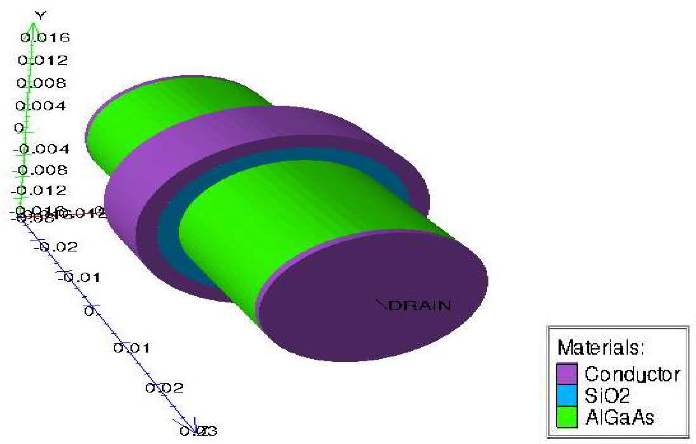
Figure 2.
Transfer characteristics of Al0.30Ga0.60As channel-based JLFET with different channel lengths.
Figure 2.
Transfer characteristics of Al0.30Ga0.60As channel-based JLFET with different channel lengths.
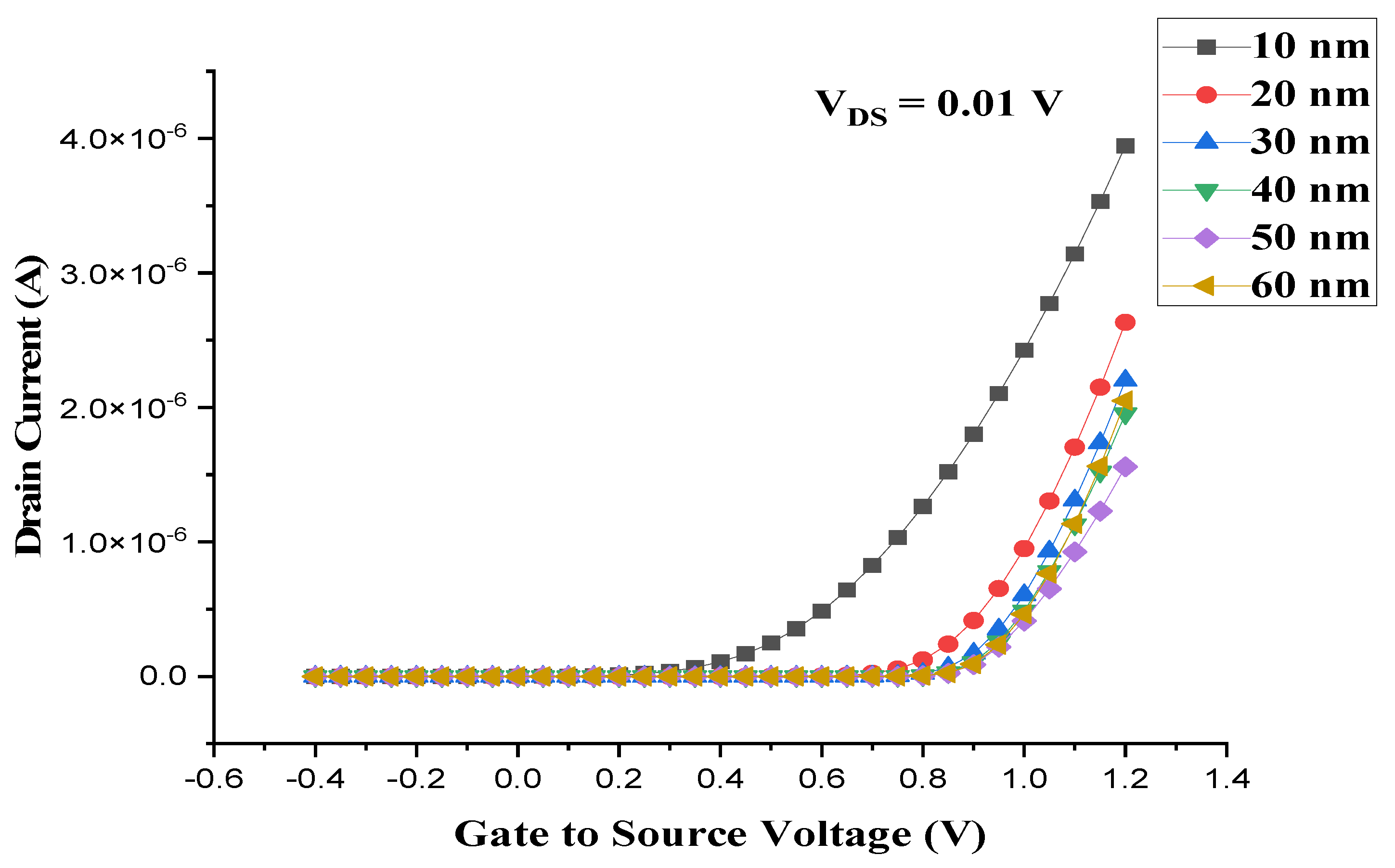
Figure 3.
Threshold Voltage variation of Al0.30Ga0.60As channel-based JLFET with different channel lengths.
Figure 3.
Threshold Voltage variation of Al0.30Ga0.60As channel-based JLFET with different channel lengths.
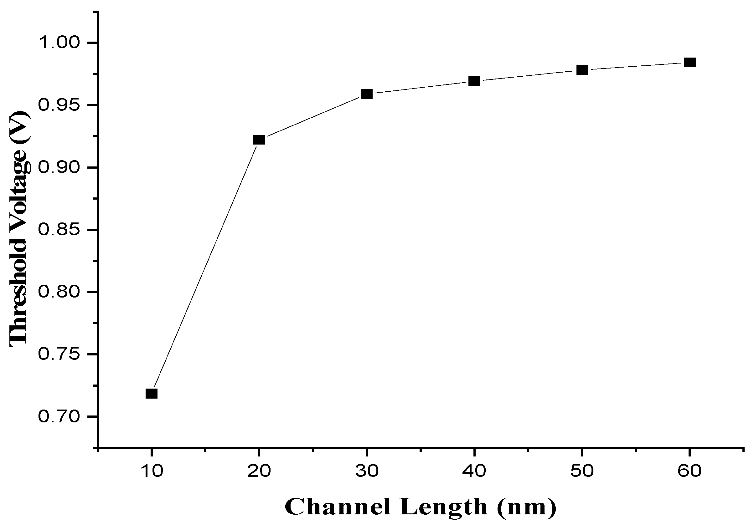
Figure 4.
Electric field distribution along the channel for Al0.30Ga0.60As channel-based JLFET.
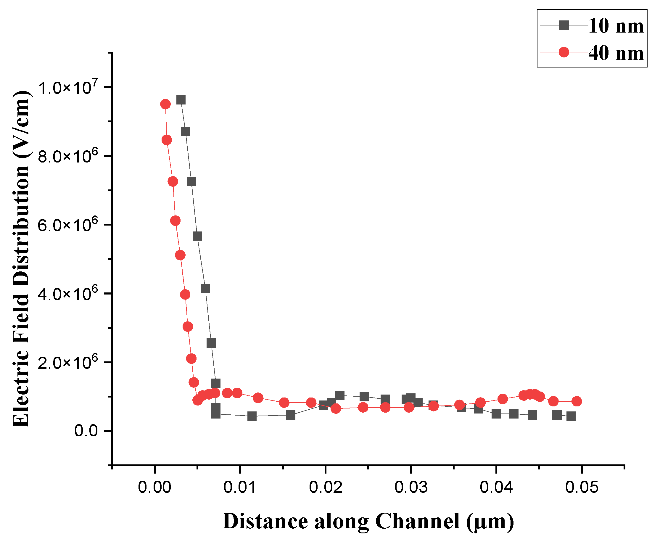
Figure 5.
Energy band diagram of Al0.30Ga0.60As Channel-based 10 nm JLFET.
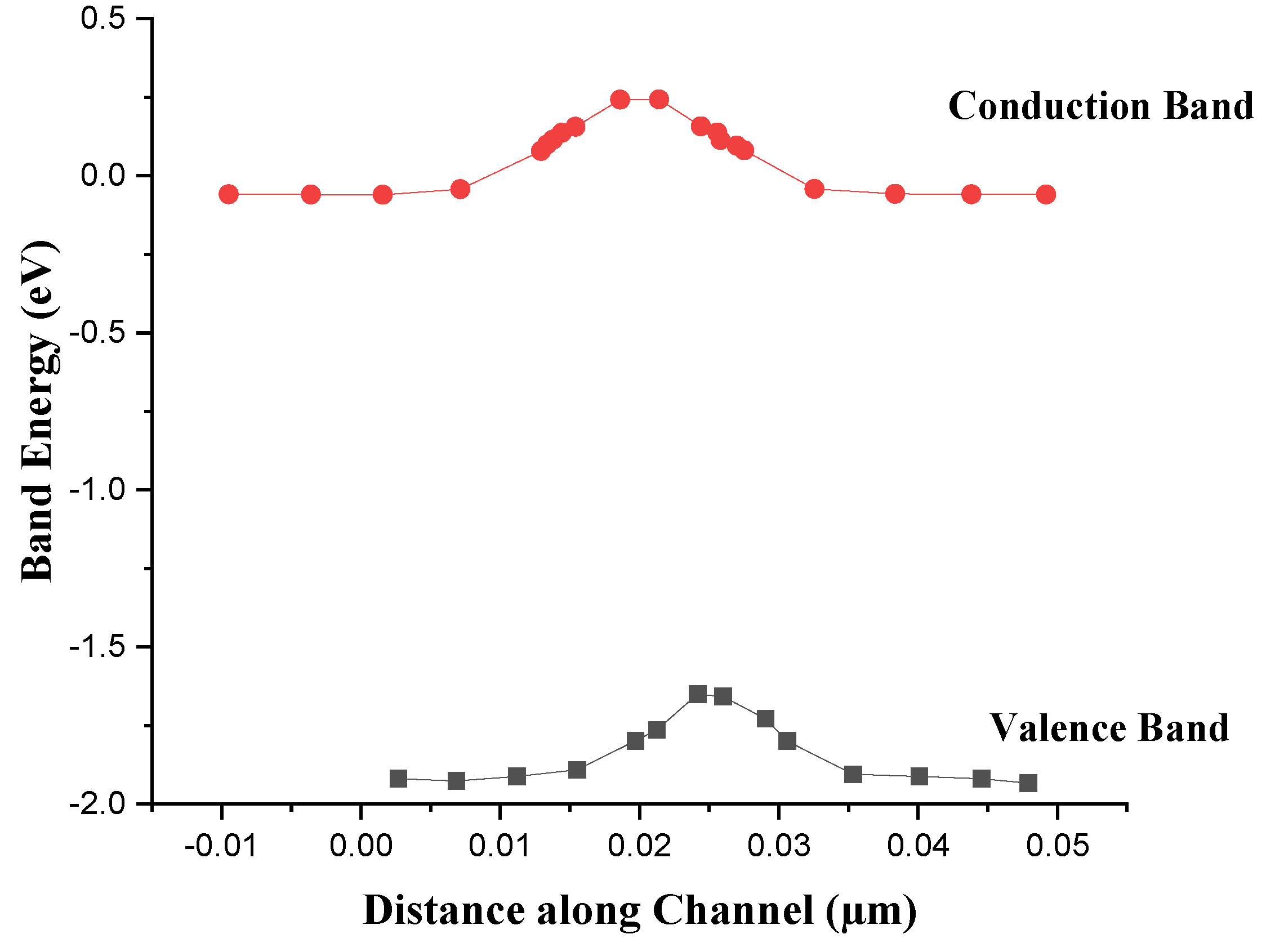
Figure 6.
Energy band diagram of Al0.30Ga0.60As Channel-based 40 nm JLFET.
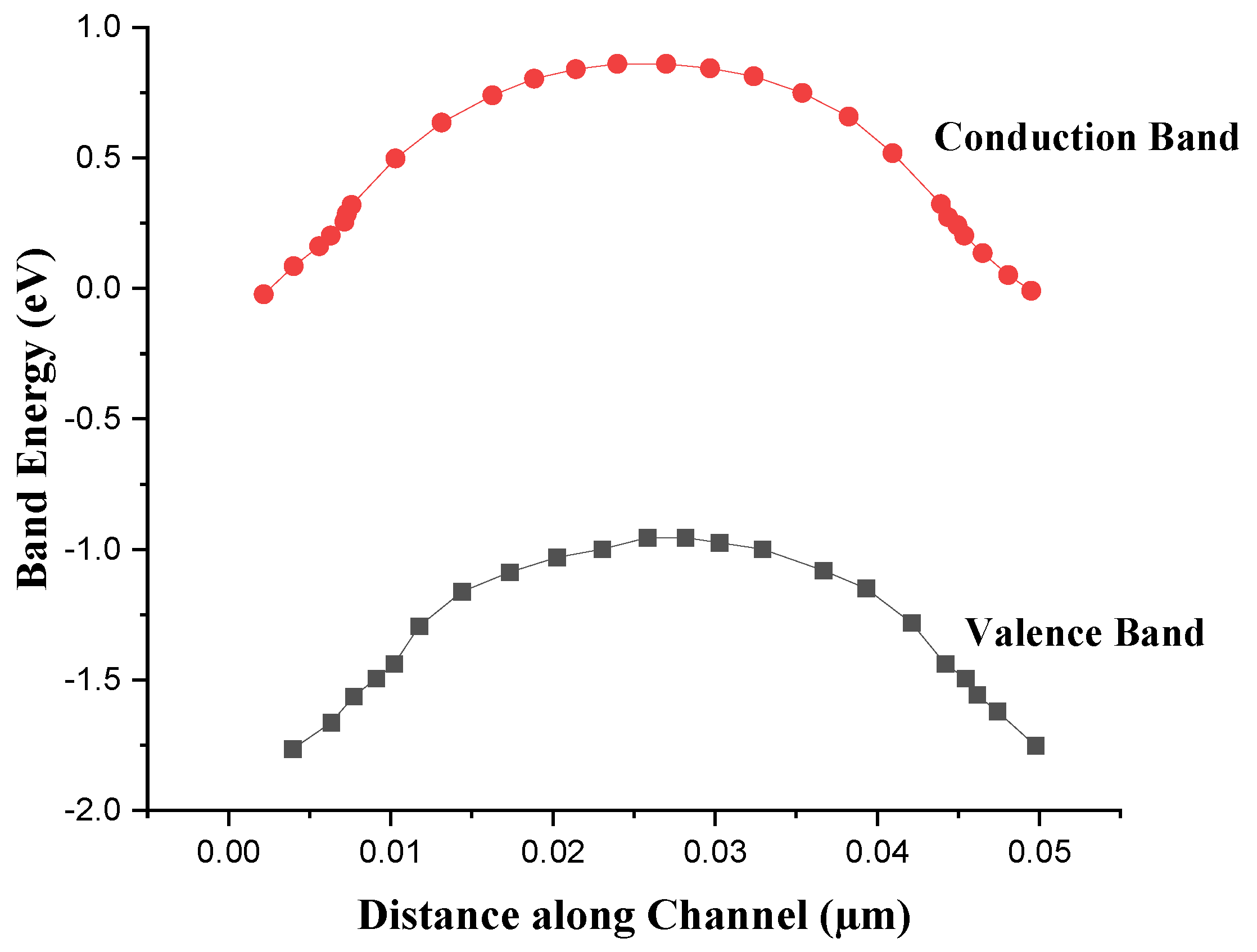
Figure 7.
Electric Potential Distribution along the channel for Al0.30Ga0.60As channel-based JLFET.
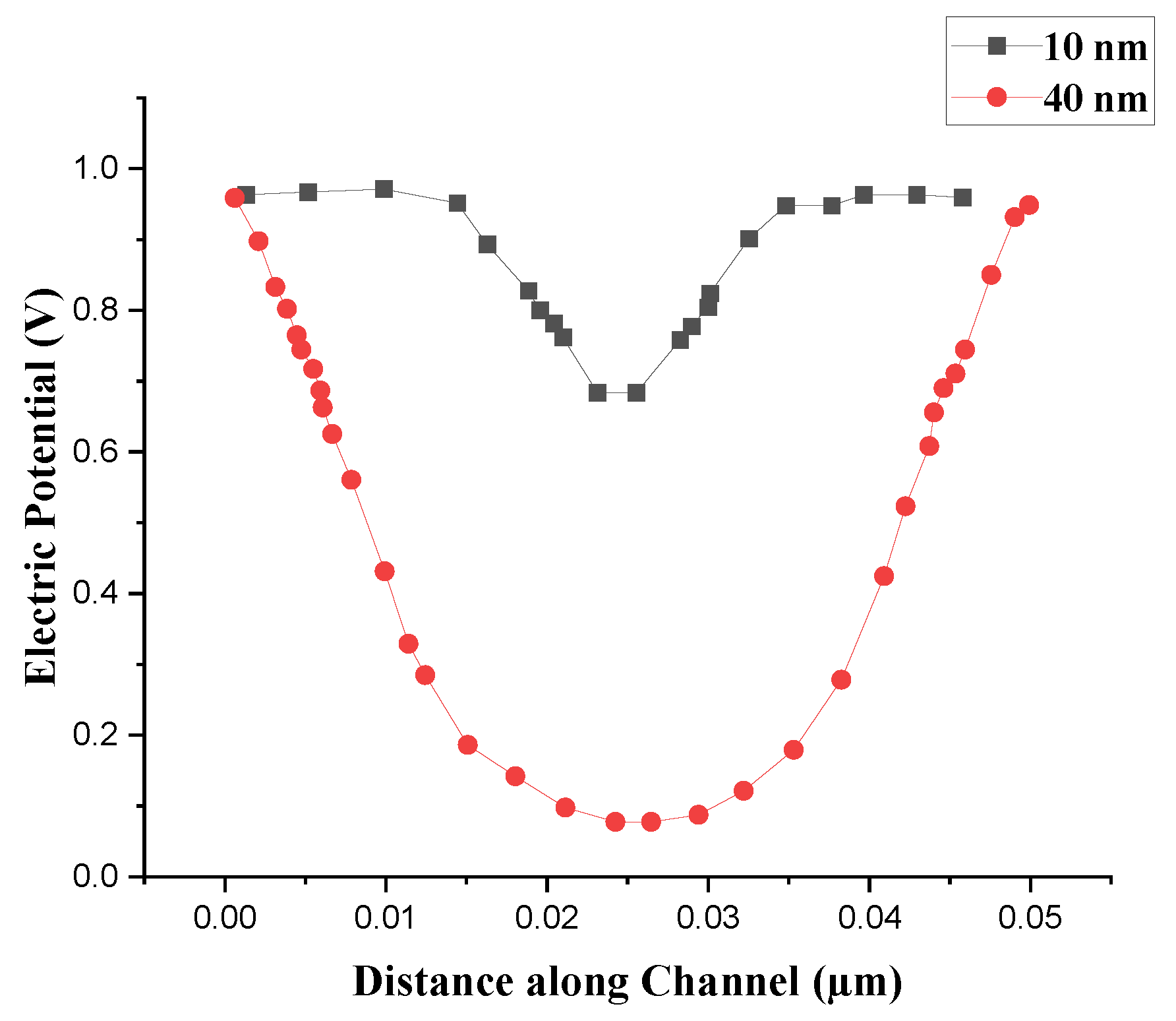
Figure 8.
Current flow lines along the channel for Al0.30Ga0.60As channel-based JLFET.
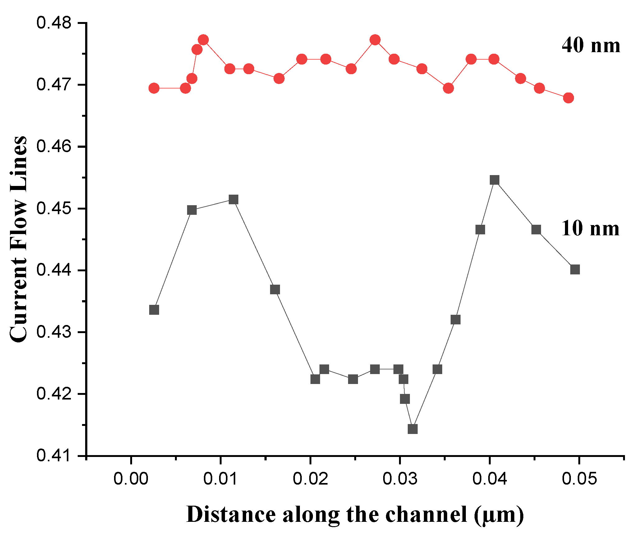
Figure 9.
Electron concentration along the channel for Al0.30Ga0.60As channel-based JLFET.
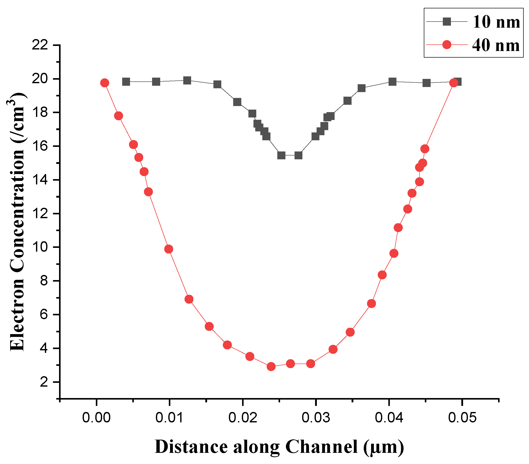
Figure 10.
Electron Mobility along the channel for Al0.30Ga0.60As channel-based JLFET.
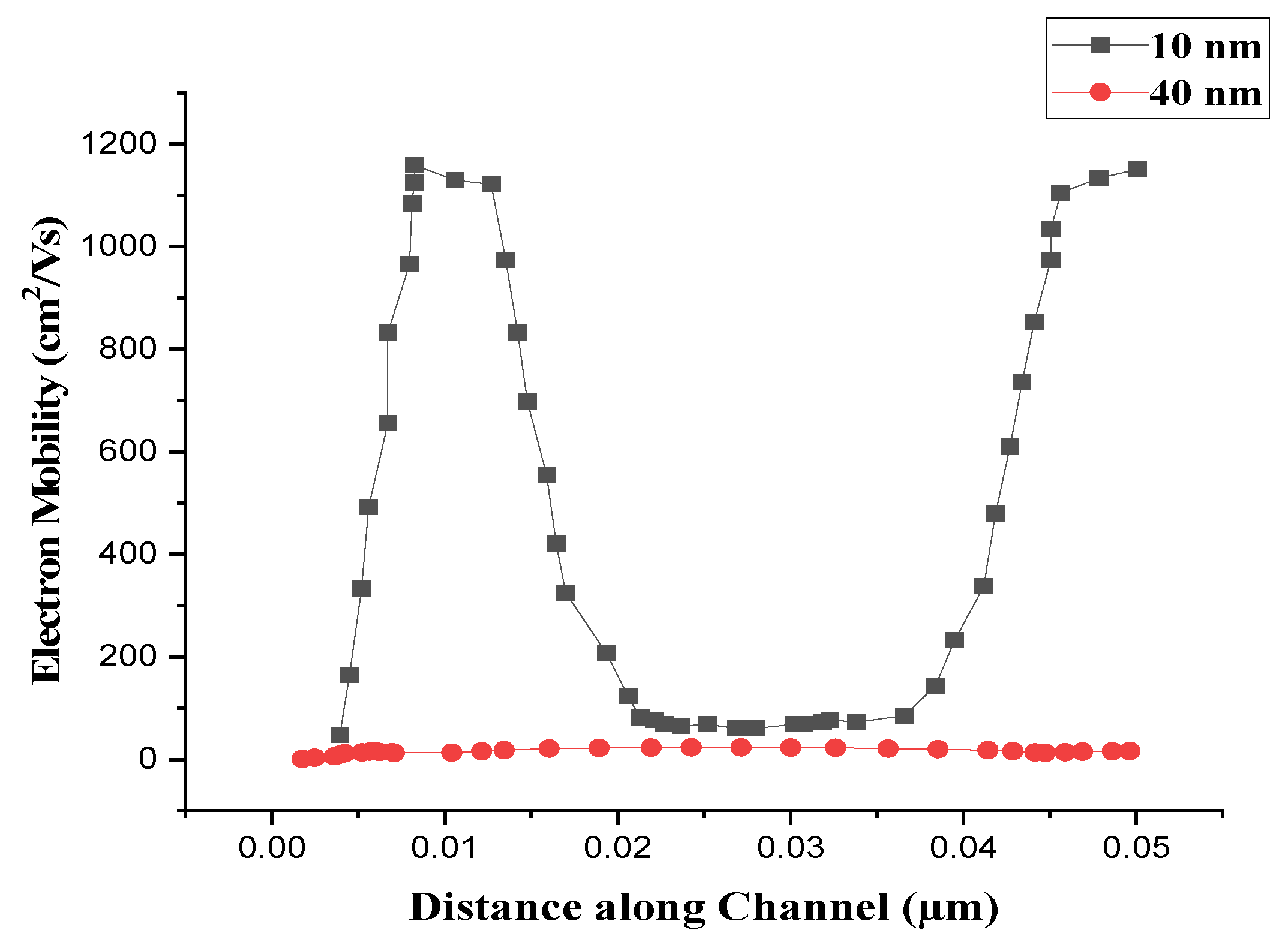
Figure 11.
Output characteristics of Al0.30Ga0.60As Channel-based JLFET with different channel lengths.
Figure 11.
Output characteristics of Al0.30Ga0.60As Channel-based JLFET with different channel lengths.
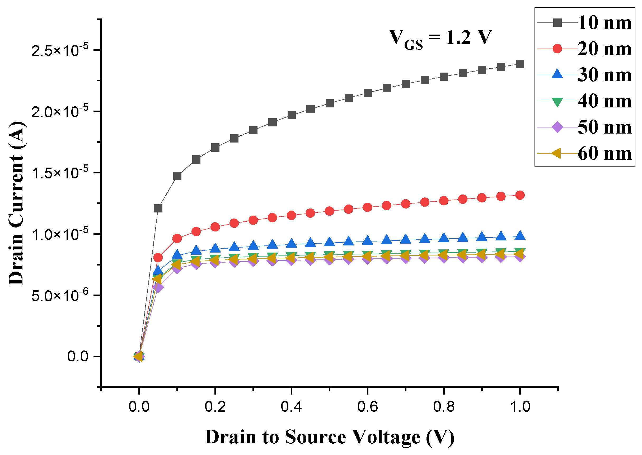
Figure 12.
SS and DIBL variation for Al0.30Ga0.60As Channel-based JLFET with different channel lengths.
Figure 12.
SS and DIBL variation for Al0.30Ga0.60As Channel-based JLFET with different channel lengths.
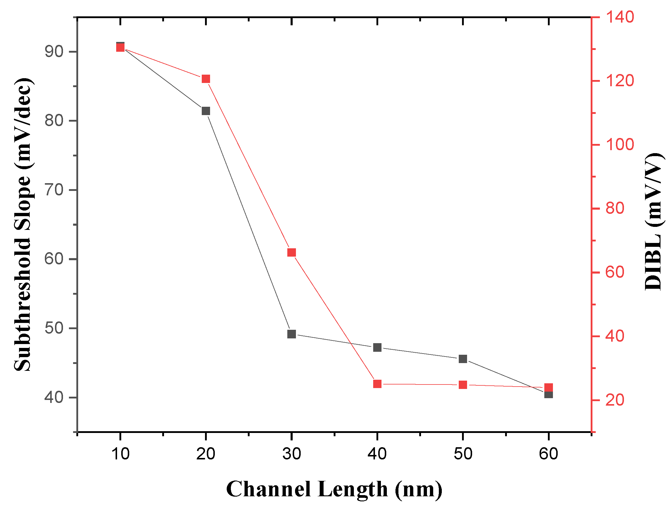
Figure 13.
On Current and Off Current variation for Al0.30Ga0.60As Channel based JLFET with different channel lengths.
Figure 13.
On Current and Off Current variation for Al0.30Ga0.60As Channel based JLFET with different channel lengths.
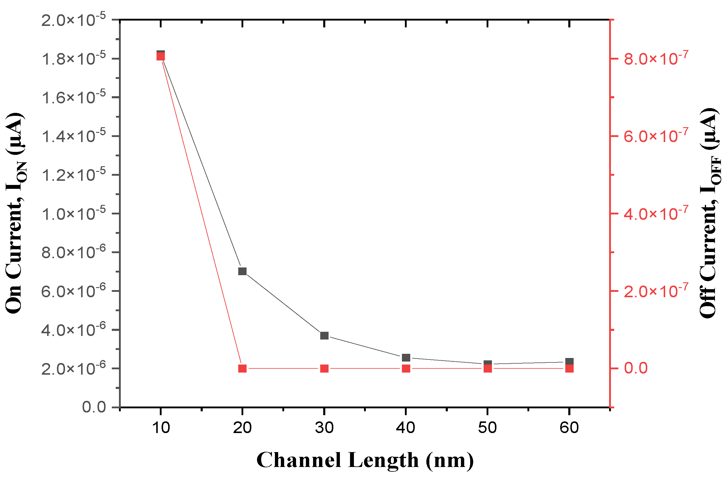
Figure 14.
Transconductance variation of Al0.30Ga0.60As Channel-based JLFET with different channel lengths.
Figure 14.
Transconductance variation of Al0.30Ga0.60As Channel-based JLFET with different channel lengths.
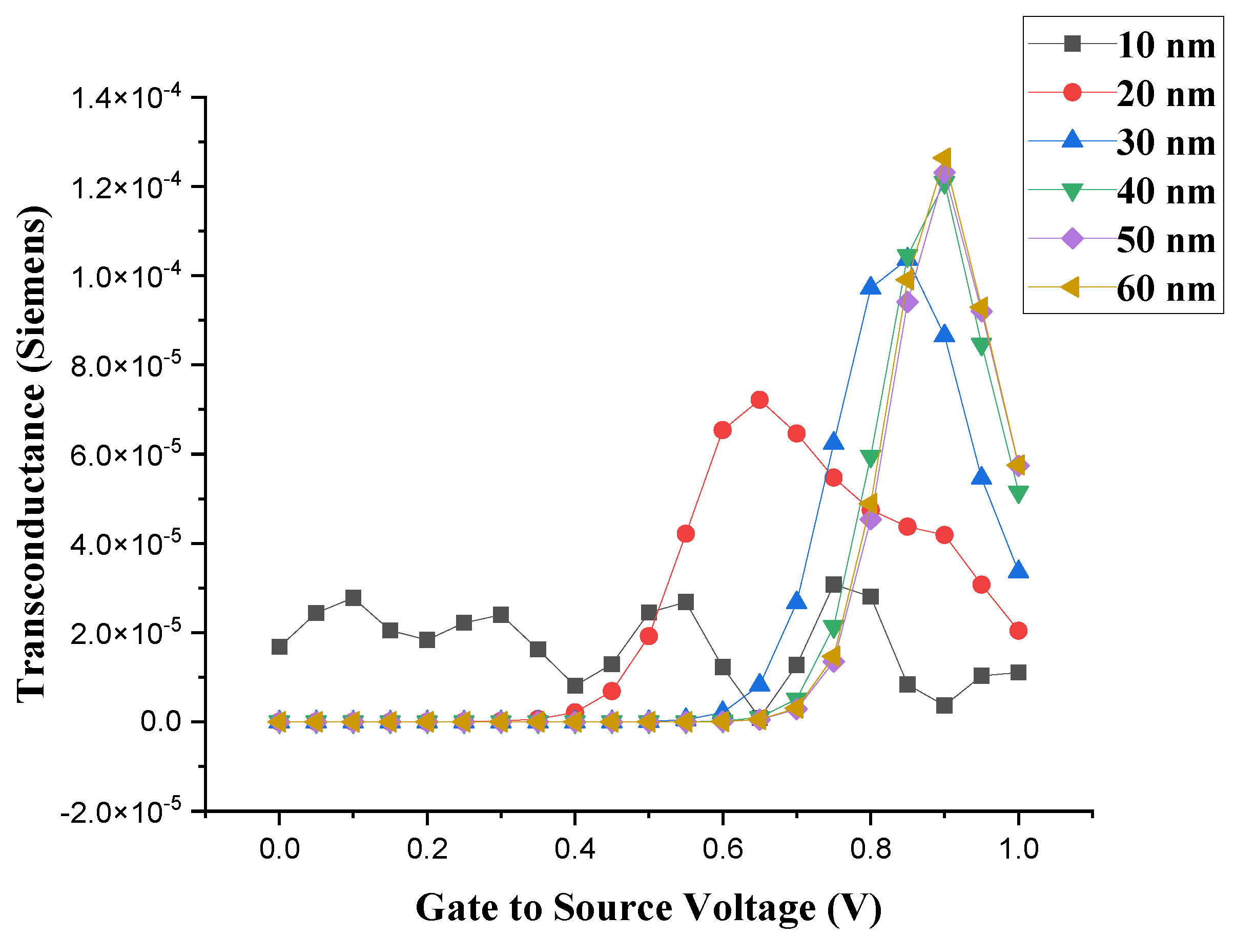
Table 3.
Device parameters.
| Parameters | For Cylindrical Gate-All-Around JLFET |
|---|---|
| Channel Material | Al0.30Ga0.60As, Aluminium Gallium Arsenide (in composite form) |
| Channel region with Doping Concentration | N-type – I019 cm-3 |
| Source region with Doping Concentration | N-type – I019 cm-3 |
| Drain region with Doping Concentration | N-type – I019 cm-3 |
| Gate material | P+ Polysilicon |
| Gate Workfunction | 5.4 eV |
| Oxide Permittivity | 3.9 |
| Channel Length | Ranges from 10 nm to 60 nm |
| Oxide Thickness | 2 nm (radius) |
| Semiconductor (Si-Substrate) Thickness | 10 nm (radius) |
| Device Length | 60 nm |
Table 4.
Fundamental Parameters of AlGaAs at 300 K.
| Crystal structure | Zinc Blende |
| Number of atoms in 1 cm3 | (4.42-0.17x)·1022 |
| Debye temperature | 370+54x+22x2 K |
| Density | 5.32-1.56x g·cm-3 |
| Dielectric constant (static) | 12.90-2.84x |
| Dielectric constant (high frequency) | 10.89-2.73x |
| Effective electron mass (me) | 0.063+0.083x mo (x<0.45) |
| Density-of-states electron mass (mcd) | 0.85-0.14x mo (x>0.45) |
| Conductivity effective mass (mcc) | 0.26 mo (x>0.45) |
| Effective hole masses (mh) | 0.51+0.25x mo |
| Effective hole masses (mlp) | 0.082+0.068x mo |
| Electron affinity | 4.07-1.1x eV (x<0.45) |
| 3.64-0.14x eV (x>0.45) | |
| Lattice constant | 5.6533+0.0078xÅ |
Table 5.
The electrical characteristics of AlGaAs.
| Breakdown field | ≈(4÷6) ·105 V/cm |
| Mobility electrons | |
| 0<x<0.45 | 8·103-2.2·104x+104·x2 cm2 V-1 s-1 |
| 0.45<x<1 | -255+1160x-720x2 cm2 V-1 s-1 |
| Mobility holes | 370-970x+740x2 cm2 V-1 s-1 |
| Diffusion coefficient electrons | |
| 0<x<0.45 | 200-550x+250x2 cm2/s |
| 0.45<x<1 | -6.4+29x-18x2 cm2/s |
| Diffusion coefficient holes | 9.2-24x+18.5x2 cm2/s |
| Electron thermal velocity | |
| 0<x<0.4 | (4.4-2.1x)·105 m/s |
| 0.45<x<1 | 2.3·105 m/s |
| Hole thermal velocity | (1.8-0.5x)·105 m/s |
Table 6.
Performance comparison of the proposed Al0.30Ga0.60As Channel-based JLFET with different channel lengths.
Table 6.
Performance comparison of the proposed Al0.30Ga0.60As Channel-based JLFET with different channel lengths.
| Lg (nm) | Vth (V) | Saturation Slope (A) | Max. Drain Current (A) | SS (mV/dec) | DIBL (mV/V) | Ion (µA) | Ioff (µA) | Ion/Ioff |
|---|---|---|---|---|---|---|---|---|
| 10 | 0.71864309 | 4.8060692×10⁻⁶ | 2.38548734 ×10⁻⁵ |
90.811026 | 130.478984 | 1.82114482 ×10⁻⁵ |
8.0515476 ×10⁻⁷ |
22.61858 |
| 20 | 0.92221857 | 2.1114994 ×10⁻⁶ | 1.31566809×10⁻⁵ | 81.4501738 | 120.697472 | 7.02601295 ×10⁻⁶ |
3.0486378 ×10⁻¹⁴ |
230464043 |
| 30 | 0.95883678 | 8.447915 ×10⁻⁷ |
9.77385934×10⁻⁶ | 49.1701421 | 66.2491032 | 3.7020172 ×10⁻⁶ |
1.85712014 ×10⁻¹⁸ |
1.99341826×10¹² |
| 40 | 0.9691365 | 4.629001 ×10⁻⁷ |
8.5672922 ×10⁻⁶ |
47.2267559 | 25.0701147 | 2.56180952 ×10⁻⁶ |
3.69007316 ×10⁻²⁰ |
6.94243558×10¹³ |
| 50 | 0.97815102 | 4.1971784 ×10⁻⁷ |
8.33677822×10⁻⁶ | 45.5820223 | 24.8246716 | 2.22791721 ×10⁻⁶ |
1.77755482 ×10⁻²¹ |
1.25336062×10¹⁵ |
| 60 | 0.98420158 | 3.1932996 ×10⁻⁷ |
8.16522822×10⁻⁶ | 40.5020524 | 23.9363979 | 2.33849879 ×10⁻⁶ |
4.15367459 ×10⁻²⁰ |
5.62995184×10¹³ |
Table 7.
Performance comparison of various III-V Channel Materials for 40 nm JLFET according to this work.
Table 7.
Performance comparison of various III-V Channel Materials for 40 nm JLFET according to this work.
| Si and III-V Material | Vth (V) | Saturation Slope (A) | Max. Drain Current (A) | SS (mV/dec) | DIBL (mV/V) |
Ion (µA) | Ioff (µA) | Ion/Ioff |
|---|---|---|---|---|---|---|---|---|
| GaAs |
0.819608 | 6.41239 ×10⁻⁷ | 2.31345 ×10⁻⁵ |
64.47608 | 30.5962 | 12.7614 | 1.125467 ×10⁻⁹ |
1.133861 ×10¹⁰ |
| InP | 0.656255 | -3.1528 ×10⁻¹⁰ |
5.02586 ×10⁻⁶ | 66.8384 | 39.4156 | 4.28187 | 3.6750 ×10⁻⁵ |
116513.47 |
| AlGaAsP | 0.799256 | 1.01434 ×10⁻⁷ |
2.91153 ×10⁻⁶ |
64.44775 | 40.81138 | 1.61177 | 1.717025 ×10⁻¹⁰ |
9.386899 ×10⁹ |
| GaN | 0.472639 | 3.99288 ×10⁻⁶ |
7.14924 ×10⁻⁵ |
68.34655 | 40.35768 | 4.91099 |
5.031638 ×10⁻³ |
9760.222 |
| InGaAsP | 0.656257 | -3.1528 ×10⁻¹⁰ |
5.02585 ×10⁻⁶ |
66.83845 | 39.41564 | 4.28188 | 3.675004 ×10⁻⁵ |
116513.47 |
| GaP | 0.552483 | 8.468 ×10⁻¹¹ |
5.02435 ×10⁻⁶ |
67.84844 | 22.50066 | 4.42848 | 3.620443 ×10⁻⁴ |
12231.8586 |
| AlGaAs | 0.819837 | 6.4125 ×10⁻⁷ |
2.31344 ×10⁻⁵ |
64.47583 | 30.59605 | 1.27615 | 1.125457 ×10⁻⁹ |
1.133872 ×10¹⁰ |
| Al0.30Ga0.60As | 0.969136 | 4.6290 ×10⁻⁷ |
8.56729×10⁻⁶ | 47.22677 | 25.07014 | 2.56184 | 3.690073 ×10⁻¹⁴ |
6.942438 ×10¹³ |
| Al0.20Ga0.80As | 0.908568 | 5.19404×10⁻⁷ | 1.29049×10⁻⁵ | 47.30019 | 28.52392 | 5.42004 | 1.260631 ×10⁻¹⁸ |
4.299456 ×10¹² |
Table 8.
Performance comparison of the proposed JLFET with other device architectures available in the literature.
Table 8.
Performance comparison of the proposed JLFET with other device architectures available in the literature.
| Device Architectures |
Authors | Materials | Lg (nm) |
SS (mV/dec) |
DIBL (mV/V) |
Ion (µA) | Ioff (µA) | Ion/Ioff |
|---|---|---|---|---|---|---|---|---|
| Cylindrical Gate-all-around JLFET (This work) | P. Srivastava et al. | GaAs |
40 | 64.47608 | 30.5962 | 12.7614 | 1.125467 ×10⁻⁹ |
1.133861 ×10¹⁰ |
| Cylindrical Gate-all-around JLFET (This work) | P. Srivastava et al. | Al0.30Ga0.60As | 40 | 47.22677 | 25.07014 | 2.56184 | 3.690073 ×10⁻¹⁴ |
6.942438 ×10¹³ |
| Cylindrical Gate-all-around JLFET (This work) | P. Srivastava et al. | Al0.20Ga0.80As | 40 | 47.30019 | 28.52392 | 5.42004 | 1.260631×10⁻¹⁸ | 4.299456 ×10¹² |
| Symmetric Double Gate JLFET | Talukdar et al. [52] | GaAs | 30 | 65 | - | - | - | - |
| SiGe Double Gate Junctionless MOSFET | Rout et al. [53] |
GaSb | 20 | 59.78 | - | - | - | 7.52 ×10¹³ |
| Compound JLFET | Cho et al. [54] |
GaAs | 40 | 90 | - | - | - | About 108 |
Disclaimer/Publisher's Note: The statements, opinions and data contained in all publications are solely those of the individual author(s) and contributor(s) and not of MDPI and/or the editor(s). MDPI and/or the editor(s) disclaim responsibility for any injury to people or property resulting from any ideas, methods, instructions or products referred to in the content. |
© 2025 by the authors. Licensee MDPI, Basel, Switzerland. This article is an open access article distributed under the terms and conditions of the Creative Commons Attribution (CC BY) license (http://creativecommons.org/licenses/by/4.0/).
Copyright: This open access article is published under a Creative Commons CC BY 4.0 license, which permit the free download, distribution, and reuse, provided that the author and preprint are cited in any reuse.


