
Submitted:
23 January 2025
Posted:
23 January 2025
You are already at the latest version
Abstract
Generating chaos from originally non-chaotic systems is a promising issue. Indeed, chaos has been successfully applied in many fields to improve systems performance. In this work, a Buck converter is chaotified using a combination of the switching piecewise-constant characteristic and of the anticontrol of chaos feedback. For electromagnetic compatibility compliance reasons, this feedback control method is able at the same time to achieve low spectral emissions and to maintain a small ripple of the output voltage and of the inductance current. This new feedback implies a fast and non-linear switching action of the Buck Mosfet on a period of the ramp generator. Thus, it is essential to analyze its thermal performance. This is why we propose an original analysis of the influence of anticontrol of chaos and switching frequency variation on the junction temperature: we investigate the correlation between the lifetime of the power electronic switching component and its thermal stress due to the addition of chaos. It appears that the reduction of the current ripple does not degrade the Mosfet junction thermal performances despite the fast switching of the Mosfet. Furthermore, an insignificant degradation of the Mosfet lifetime is indicated for chaotic behavior versus periodic behavior. Thus, this leads to the conclusion that using anticontrol of chaos produces insignificant accumulated fatigue effect of the Buck converter’s semiconductor.
Keywords:
SiC MOSFET
; anticontrol of chaos
; electrothermal model
; power losses
; lifetime
1. Introduction
Chaos has been extensively studied by a large scientific community as an interesting complex dynamic phenomenon. Firstly, chaos was analyzed as a phenomenon that can occur naturally by variations of system parameters [1,2]. For example, a Buck converter can exhibit a chaotic behavior with the variation of the current reference [3,4], the inductance [5] of the converter, the load [6], the voltage reference [7] or a control parameter [8,9].
Recently, chaos has evolved to a new phase of control (i.e. suppressing of chaos), utilizing chaos or the generation of chaos from an originally non-chaotic system. The goal of purposefully causing chaos (a shift from order to chaos), also known as chaotification or anticontrol of chaos, has garnered a lot of interest lately because of its enormous potential in unconventional applications with opportunities to employ entirely novel and different strategies.
Numerous chaotic and nonlinear events have been seen in optical or physical systems. Reference [10] examines how the parallelly and orthogonally polarized intensity-modulated optical injection on vertical-cavity surface-emitting lasers is affected by the chaotic dynamic behaviors of injection strength, frequency detuning and modulation parameters (modulation depth and modulation frequency). A traditional electro-optic intensity chaotic model is used to propose an electro-optic linked mutual injection chaotic system in [11].
From the conventional tendency of comprehending and analyzing chaos to using it, the study of chaotic dynamics has changed, such as on financial time series. The authors of [12] analyze the chaotic characteristics and predictive modeling of the daily price time series of West Texas Intermediate crude oil from 2009 to 2019. Utilizing chaos theory and artificial intelligence techniques, they analyze the time series and assess the impact of noise on price forecasting accuracy.
The anticontrol of chaos has attracted growing interest for applications in secure transmission as image encryption. An image encryption method based on the anti-control method is designed in [13], and the encryption algorithm with chaotic position scrambling and stream cipher encryption for multi-rounds is established. As demonstrated in [1], chaos synchronization does not necessarily require broadband couplings, as the damped resonance can be entrained even with frequency-limited coupling. This insight allows to future applications of chaos-based communication using practical antennas, particularly in areas like distributed sensing. Later, in 2023, Erkan, Ogras and Fidan [14] propose a secure data transmission application using a modulation-based transceiver circuit: an encryption key was generated using a chaotic logistic map and embedded into both the transmitter and receiver circuits. These circuits were configured with identical system parameters to ensure synchronization and secure communication. Then, an encryption-and-compression-based technique for medical images is proposed by [15]. After a comprehensive cryptanalysis, [16] identifies that a chaotic image encryption scheme based on a variant of the Hill cipher is vulnerable to both chosen-plaintext and chosen-ciphertext attacks due to inherent structural weaknesses in its design.
The route to chaos is very impressive in biological and medical systems. The authors of [17] explore a computational dynamic solution as a possible therapy for epileptic seizures control. A neuronal model of epileptiform activity is chaotified and executed before the seizure starts. More recently, bifurcation theory has been employed to analyze the progression of diseases by investigating new fractional-order models of six chaotic diseases [18]. In order to suppress chaos, back-stepping, adaptive feedback and sliding mode control strategies are used in fractional-order models of Diabetes Mellitus, Human Immunodeficiency Virus, Ebola Virus and Dengue models. The anticontrol of chaos with linear state feedback, single state sine feedback and sliding mode anticontrol is designed in fractional-order models of Parkinson’s illness and migraine. To investigate the neuromorphic dynamics of memristive neurons, [19] proposes a tri-stable locally active memristor model via Chua’s unfolding principle. This study shows that memristive circuits can generate diverse neuromorphic patterns within the right-half plane domain, particularly near the edge of chaos, highlighting their potential for modeling complex neuronal behavior. In contrast, [20] develops a theoretical model of gene expression dynamics that reveals chaotic behavior emerging from rapid molecular feedback loops coupled with cell growth dynamics and intercellular interactions. This chaotic behavior is proposed as an explanation for the heterogeneous responses of Escherichia coli cells to oxidative stress. Both studies emphasize the critical role of chaos in understanding complex systems, from artificial neurons to biological gene regulation.
In the field of electrical systems, [21] proposes an anti-oscillation (control of chaos) scheme for a fractional-order brushless DC motor system. This approach aims to eliminate chaotic oscillations in systems with unknown dynamics and immeasurable states, ensuring stable operation by effectively suppressing chaotic behavior. Similarly, [22] introduces the modified chaos grasshopper algorithm, an advanced optimization approach. This algorithm is applied to improve the performance of techno-economic energy management strategies in microgrids incorporating fuel cells, batteries, and photovoltaic systems. A chaos learning butterfly optimization technique with enhanced extraction of the photovoltaic model parameter is presented in [23]. Following a numerical evaluation of the second-law characteristics of a solar water heater with a dual-twisted tape turbulator, [24] uses nonlinear calibration with chaos control to establish a thermal energy prediction model for varying Reynolds number and twist pitch values.
Switch-mode power supplies produce electromagnetic interference (EMI) at their switching frequency and harmonic frequencies. This interference significantly complicates achieving electromagnetic compatibility (EMC), especially when employing pulse-width modulation (PWM) techniques. The modulation of the switching frequency, as presented by [25] and [26], is a technique aimed at reducing spectral emissions. In 1999, Deane further proposed the innovative idea of using chaos to improve electromagnetic compatibility by diminishing spectral peaks [27]. However, the application of the classical chaos anticontrol method to switch-mode power supplies increases the overall magnitude of output voltage ripple, a result corroborated later by [28]. In contrast, [29] and [30] introduced a chaotified nonlinear feedback approach capable of achieving low spectral emissions while maintaining minimal output voltage ripple by employing chaotic attractors of small dimensions. More recently, [31] proposed a chaos-based pulse-width modulation technique that leverages the logistic map to distribute the harmonics of a Boost converter, effectively reducing electromagnetic interference. Building on these advancements, [32] introduced a novel radio frequency transmitter that utilizes a chaotic sequence generator to minimize output signal hysteresis and applies a modulation process to reduce spectral emissions. Additionally, [33] studied a high-frequency isolated quasi Z-source photovoltaic grid-connected micro-inverter employing chaotic frequency modulation technology to suppress inverter spectral emissions effectively.
The anticontrol of chaos feedback necessitates rapid switching actions in converters, which impose thermal stress on power-switching semiconductor devices [34]. Consequently, it becomes critical to analyze their thermal performance to ensure operational safety and prevent failures of power devices [35]. To evaluate the efficiency and reliability of power electronic systems, semiconductor devices are often modeled as ideal switches in fast simulations, as seen in [36]. However, this approach makes it challenging to accurately calculate MOSFET power losses. Establishing an electro-thermal model [37] is essential to account for the impact of junction temperature on the device parameters.
Numerous electro-thermal models have been presented in scientific literature. For approximating IGBT switching and on-state losses, [38] employed the lookup table method. Using inputs such as junction temperature and electrical load, a complete and comprehensive electro-thermal model is proposed by [39]. Similarly, the model by [40] incorporates the interactions between junction temperature and the transistor’s voltages and currents. In [41], power losses are averaged across each switching cycle using a high-speed electro-thermal model. Furthermore, [42] and [43] developed a realistic converter model, with parameters derived from component datasheets, PCB layout, as well as cable length and diameter.
To analyze the Mosfet thermal behavior, the most prevalent heat transfer model uses several Foster [44,45] networks. In [46], Nayak and Pramanick utilized a third-order Foster circuit to accurately fit the MOSFET impedance curve provided in the datasheet. Additionally, [47] proposed various electro-thermal Foster circuit variants to simulate the performance of an electric vehicle inverter.
Changes in the power device junction temperature affect their reliability and lifetime, according to [48]. The Coffin-Manson law is one of the most widely used models for evaluating failure cycles and estimating the lifetime of switching devices. Inverter lifetime [49] is commonly assessed using the rainflow counting algorithm, which takes as inputs the mean junction temperature and the variation on junction temperature [50,51], and [52]. In [53], an analysis is presented on the influence of chaos on junction temperature, revealing that a chaotic current behavior reduces the MOSFET’s lifetime by half, compared to periodic current behavior.
After a chaotification of a Buck converter (in order to reduce spectral emission), the purpose of this article is to analyse the influence of an anticontrol of chaos controller on the junction temperature and to compare it with a standard feedback (PID controller). The anticontrol of chaos feedback (a combination of anticontrol of chaos and PID standard controller) is capable of simultaneously achieving low spectral emissions while maintaining minimal ripple of both the output voltage and the inductor current. Mosfet fast and non-linear switchings cause thermal stress. We propose in this study to investigate the correlation between the lifetime of a C2M0080120D Mosfet [54] and its thermal stress due to the anticontrol of chaos and the switching frequency variation. The reduction of the current ripple enhances the Mosfet junction thermal performances. A step-by-step process establishes the electro-thermal model of the Mosfet integrating power losses (which includes the conduction, switching losses, diode conduction and reverse recovery losses). Finally, the Miner’s model accumulated stress of the Mosfet is quantified evaluating the number of failure cycles by the Coffin–Manson equation and the thermal cycles numbers using the rainflow counting algorithm. Then, the accumulated fatigue shows an insignificant degradation of the Mosfet lifetime with anticontrol of chaos feedback (in comparison to a standard controller) despite the fast switching of the Mosfet. Thus, this leads to the conclusion that using anticontrol of chaos does not degrade the remaining life (i.e. it has an insignificant aging effect) of the Buck converter’s semiconductor.
The main sections of this paper are: Section 2 describes the behavior of a Buck converter both with a standard and anticontrol of chaos controller. In Section 3, the Mosfet power loss calculations and thermal model are detailed. Then, in Section 4, the lifetime model estimating the damage on a Mosfet is presented. The paper concludes in Section 5.
2. Nonlinear Behavior of a Buck Converter
In this paper, our study is focused on a Buck converter, which topology is shown in Figure 1. The circuit consists of an inductance L, a diode D, a Mosfet switch (C2M0080120D), a capacitance C and a load R. The output voltage tracks the reference signal , ensuring the desired stabilized output voltage.
When the Mosfet is in on-state, the energy is stored in the inductance L and in the capacitance C and no current flows through the diode D. When the Mosfet is in off-state, the diode now conducts, ensuring a path for the inductor current . The Buck converter uses a periodic switching to step down the input voltage . This is achieved by controlling the power Mosfet using a pulse width modulated signal. This signal is generated using the error amplifier (i.e. the deviation between the output voltage and a reference voltage), a Proportional Integral Derivative (PID) controller and the ramp input voltage (characterized by and ) to adjust the duty cycle of the switch.
Despite the continuous advances in control theory, the PID controller still is the most popular control technique employed in feedback control for regulating the output voltage of Buck converters. The standard structure of the controller is as follows:
where P, I, D and N are the proportional, the integral, the derivative and the filter coefficients. The parameters of the converter are selected to achieve the desired output voltage.
The inductance current and the Mosfet current of this circuit are generally periodic at the switching frequency (f=10 kHz), as shown in Figure 2. The simulation results show that and Mosfet current increase from 15.25 A to 16.75 A when the Mosfet is in on-state. Consequently, the Mosfet mean current is 16 A, with a ripple of 1.5 A. If the Mosfet is in off-state, decreases, meanwhile the Mosfet current is zero.
Figure 3(a) shows the periodic output voltage with a 2.5 V ripple. Its spectrum, shown in Figure 3(b), corresponds to the converter governed by the control law of Equation (1). The spectrum consists solely of the fundamental frequency, characterized by a sharp peak at , with a magnitude of -25 dB, and its harmonics.
Now, let us introduce the controller with the following control law:
This time, the controller (2) includes, in addition to PID, a nonlinear feedback controller, with a multiplication of the feedback introducing the chaos voluntarily. The amplitude and frequency of the resulting control signal dictate the number of switching cycles of the MOSFET. Figure 4 present the simulation results for and the Mosfet current obtained with the controller (2). and Mosfet currents vary irregularily between 15.6 A to 16.4 A. Consequently, the Mosfet mean current is 16 A, with a very small ripple of 0.8 A. The Mosfet switches much more frequently that in the previous case (when the converter operates under the control law of Equation (1)), but not periodically any more. This allows to maintain a small ripple of .
The output voltage is now chaotic, with a 1.8 V ripple, as shown in Figure 5(a). Therefore, the influence of the controller (2) on the ripple is not negligible. Figure 5(b) represents the power spectrum of with a peak of -46 dB magnitude at the switching frequency .
The various frequencies in stem from its highly irregular waveform, caused by the intrinsic nonlinear dynamics. These dynamics are driven by the varying on and off durations of the MOSFET switch within each ramp period T. Generally, the power spectrum represents the frequency components at a height given by the peak amplitude of at different frequencies. The link between the ripple and power spectrum magnitude explains the decrease of the peak magnitude from -25 dB to -49 dB. Therefore, the anticontrol of chaos improves the spectral emissions by further reducing spectral peaks. We observe that the spectrum is no longer composed of a single peak at the switching frequency (or its harmonics). Instead, numerous spectral lines appear, with a continuous power spectrum characteristic of chaos. Naturally, the reduction in the maximum of the power spectrum is achieved by the presence of chaos, increasing the converter’s switching frequency. As a result, exhibits improved frequency-domain (spectral) and time-domain (ripple) performance compared to the first case.
Figure 6 and Figure 7 show the periodic and the chaotic output voltage with f = 20 kHz. The influence of the control law (2) and the switching frequency f reduce more that 96% the ripple of from 0.8 V to 0.025 V. The chaotification of the feedback decreases the power spectrum of to -79 dB, to be compared to the -40 dB with a periodic behavior. A further increase switching frequency at f = 50 kHz leads to the same trend: ripple is 0.15 V with a periodic behavior and 7.5 mV with a chaotic behavior. The maximum of the power spectrum is reduced from -60 dB to -98 dB as shown in Figure 8 and Figure 9.
Table 1 summarizes ripple and power spectrum of the output voltage, using the control laws of Equation (1) and Equation (2) as feedback. The control law of Equation (1) leads to a large ripple. Chaotifying the converter with the proposed control law of Equation (2) as feedback ensures a good ripple and causes a spectacular decrease of the power spectrum amplitude. Finally, Table 1 shows that the power contained in the peaks harmonics of the output voltage decrease at different frequencies f = 10 kHz, 20 kHz and 50 kHz.
3. Power Loss Computation and Thermal Model
The conduction and switching losses of the MOSFET added to the power losses of the diode are the total power losses, as shown in Figure 1.
3.1. Mosfet and Diode Power Loss Computation
The MOSFET’s conduction power loss is calculated as the product of the drain-source current flowing through the MOSFET during conduction and the drain-source voltage across it at each time step, as , where . The fittype and fit MATLAB functions are used to identify the voltage at two different temperatures, C and C using the current–voltage characteristics - (Figure 10(a)), as in the following equations:
where a = 2.44 ·, b = -0.001024, c = 0.09757, d = -0.1043 for C and a = 6.636 ·, b = -0.002202, c = 0.1729, d = -0.0759 for C. The lookup table method is utilized to approximate both conduction and switching losses for the Mosfet and diode. A 2-D lookup table using temperature and current as breakpoint inputs interpolates the voltage for any given and values, based on Equation (3). Then, the conduction power loss is the product of and .
The C2M0080120D datasheet provides the dependence of switching energy losses on temperature (showing significant variation in junction temperature at a drain-source current of 20 A and a drain-source voltage of 800 V), current (exhibiting substantial variation in drain-source current), and voltage (for drain-source voltage values of 600 V and 800 V). The lookup table interpolates these known values to estimate switching energy losses at different data points.
Figure 10(b) presents the switching loss energie when the device turns-on and when the device turns-off. The fitting function for the datasheet points, as represented in this figure, is:
where e = 0.6553, f = 8.452, g = 75.04 for the on-state of the MOSFET, e = 0.4597, f = - 9.768, g = 72.87 for the off- state of the MOSFET.
The switching loss energies when the Mosfet turns-on or off depend on , and . Based on Equation (4), a 3-D lookup table having , and as inputs interpolates at any , and . Then, the loss energies are used to estimate switching power losses as the product of the loss energies and the switching frequency.
The conduction power loss of a diode is analogous to that of a MOSFET, calculated as the product of the forward saturation voltage and the forward saturation current : , where . Figure 11 presents a comparison between the datasheet points of the diode characteristic and the fitted curve, achieved with the following polynomial fitting function:
where h = 0.4481, i = - 1.187, j = - 0.1057, k = 0.6399 for C and h = 0.3296, i = 0.708, j = - 4.211, k = 2.078 for C. In order to estimate the conduction power loss , a 2-D lookup table interpolates the voltage (the output of 2-D lookup table) for any and values (the breakpoint inputs of 2-D lookup table).
The diode contributes to the switching energy due to the reverse recovery charge during turn-off of the MOSFET. is defined as the product of and the diode forward saturation voltage . In [37], the following relation is used for :
where is the peak reserve recovery current, S is the snappiness factor and is the turn-off switching rate. The snappiness factor S is 4.928, calculated from the datasheet information as (C) = 152 nC and / = 1950 A/s. In order to calculate at = C, /dt is 1090 A/s as in [37], resulting a value of 271.93 nC. depends on as follows:
A 3-D lookup table, using , and as breakpoint inputs, calculates through interpolation. The diode’s switching power loss, , is then determined as the product of the loss energies and the switching frequency.
3.2. Thermal Model
The Mosfet junction temperature is estimated by a linear model given by , where is the thermal impedance, is the ambient temperature and represents the total power loss, which is the sum of all power losses (, , and ). The thermal impedance is graphically provided in the datasheet of SiC C2M0080120D Mosfet (Figure 12(a)). By implementing curve-fitting identification of , the Foster thermal network (a resistor and capacitor thermal network as shown in Figure 12(b)) is derived. The parameters of the Foster model are = 0.2525 K/W, = 0.18024 K/W, = 0.0342 K/W, = 0.1976 K/W, = 0.42068 Ws/K, = 0.05191 Ws/K, = 0.001285 Ws/K, = 0.006952 Ws/K. The total power losses are processed through the Foster network, resulting in the junction temperature .
Figure 13(a) illustrates a stable 1T limit cycle of junction temperature using the control laws of Equation (1) as feedback with the switching frequency f = 10 kHz. has a periodic waveform with variations from 64.C to 65.C. Therefore, the mean junction temperature is near to = C, and the junction temperature variation is = 0.C. The anticontrol of chaos controller (2) forces a chaotic behavior of the junction temperature , as in Figure 13(b). The mean junction temperature is near to = 65.C with variations from 64.C to 65.C, meanwhile the variation of temperature is = 1.C. The stable and chaotic behaviors of junction temperature at others frequencies f = 20 kHz and 50 kHz are presented on Figure 14 and Figure 15.
Figure 13, Figure 14 and Figure 15 show how different controllers of the Buck converter (at different frequencies) impact the junction temperature evolutions (the stable period-1T and chaotic behaviors), however with an insignificant impact on mean junction temperatures and their variations. This is explained by the presence of the same mean current of the on-state Mosfet.
Even the Mosfet switchings only one time on the T period with controller (1) and many times with controller (2), the total power losses is nearly the same in both cases. It must be mentioned that the three power losses , and are a hundred times smaller than . The latter is proportional to the conduction time when the Mosfet is in on-state. The only conduction time on the T period of the first case (using controller (1)) is similar to the sum of a multitude of times when the Mosfet is in on-state on the T period of the second case (using controller (2)).
4. Remaining Life Estimation
A thermal cycle counting algorithm is applied to the junction temperature in order to predict the power Mosfet remaining life. The most widely used algorithm is rainflow counting: it converts the time series of the junction temperature into a number of cycles, thereby facilitating lifetime prediction. In Figure 16(a), the rainflow histogram presents one value of thermal cycles of 3000× due to the periodicity. However, if the time series of the junction temperature is irregular or chaotic, the result of the rainflow counting algorithm is a set of organized cycles with a maximum of 120×, as in Figure 16(b).
Figure 17 and Figure 18 present the thermal cycles of the stable and chaotic behaviors of junction temperature at others frequencies f = 20 kHz and 50 kHz.
These results are used to derive the Mosfet accumulated fatigue Q using the Miner’s rule. It is expressed as:
where represents the number of cycles calculated using the rainflow counting algorithm, and is the number of cycles to failure. For the estimation of the device failure cycles, the Coffin–Manson equation is employed. It can be written as:
where is the activation energy, A and are experimental coefficients and k is the Boltzmann constant (8.617× eV/K). As in [53], the next numerical values are obtained: = −4.4887, = 0.0667 and A = 2.8823 × for a C2M0080120D Mosfet. With these coefficients and according to relation (9), the number of cycles to failure is: for the stable period-1T behavior =3.9064× cycles calculated for = C and a extremely small = 0.C; for the chaotic behavior, according to = 65.C and = 1.C, is found to be 1.2548×. The degradations of the C2M0080120D Mosfet device at others frequencies are summed up in Table 2.
The accumulated fatigue is insignificant for a stable period of the junction temperature , indicating a small impact on the remaining life of Mosfet. However, only minimal damage is observed when the anticontrol of chaos feedback is applied. The repercussions of the chaotic temperature are insignificant for the Mofset thermal stress and reliability performance. The accumulated fatigue results shows the low and high frequency thermal cycles contribute in the same way to the aging of the Buck converter’s semiconductor.
5. Conclusion
The target of the paper is to investigate the effects of the voluntary introduction of chaos into a Buck converter on the remaining life of power electronic switching components and their thermal stress. Indeed, a combination of the anticontrol of chaos feedback with a standard PID controller introduces chaos in the circuit. The resulting effects involve complex dynamical behaviors with a multitude of opportunities for special properties: maintain a small ripple of the output voltage or even reduce it, keep a small swing current amplitude of the Mofset and decrease spectral emissions. The results indicate that chaos neither impacts the mean junction temperature nor its variations. Then, counting the thermal stress cycles enables to point out that the accumulated fatigue shows an insignificant degradation of the Mosfet lifetime with anticontrol of chaos feedback (in comparison to a standard controller) despite the fast switching of the Mosfet. Thus, this leads to the conclusion that using anticontrol of chaos does not degrade the remaining life (i.e. it has an insignificant aging effect) of the Buck converter’s semiconductor.
Author Contributions
Conceptualization, C.M.; Methodology, C.M.; Software, C.M.; Validation, C.M. and J.-Y.M.; Writing original draft preparation, C.M. and J.-Y.M.; Writing review and editing, C.M. and J.-Y.M. All authors have read and agreed to the published version of the manuscript.
Funding
This research received no external funding.
Data Availability Statement
The data are available upon request to the corresponding author.
Conflicts of Interest
The authors declare no conflicts of interest.
References
- Minati, L.; Innocenti, G.; Mijatovic, G.; Ito, H.; Frasca, M. Mechanisms of chaos generation in an atypical single-transistor oscillator. Chaos, Solitons and Fractals 2022, 157, 111878. [Google Scholar] [CrossRef]
- Chen, X.; Long, X.; Hu, W.; Xie, B. Bifurcation and chaos behaviors of Lyapunov function controlled PWM boost converter. Energy Rep. 2021, 7, 163–168. [Google Scholar] [CrossRef]
- Zamani, N.; Ataei, M.; Niroomand, M. Analysis and control of chaotic behavior in boost converter by ramp compensation based on Lyapunov exponents assignment: theoretical and experimental investigation. Chaos Soliton Fractals 2015, 81, 20–29. [Google Scholar] [CrossRef]
- Dhifaou, R.; Brahmi, H. Fast Simulation and Chaos Investigation of a DC-DC Boost Inverter. Complexity 2021, 9162259. [Google Scholar] [CrossRef]
- Ghosh, A.; Banerjee, S.; Basak, S.; Chakraborty, C. A study of chaos and bifurcation of a current mode controlled flyback converter. In Proceedings of the IEEE 23rd International Symposium on Industrial Electronics (ISIE), Istanbul, Turkey, 1–4 June 2014. [Google Scholar]
- Morel, C.; Akrad, A.; Sehab, R.; Azib, T.; Larouci, C. Open-Circuit Fault-Tolerant Strategy for Interleaved Boost Converters via Filippov Method. Energies 2022, 15, 352. [Google Scholar] [CrossRef]
- Morel, C.; Morel, J.-Y.; Danca, M.F. Generalization of the Filippov method for systems with a large periodic input. Math. Comput. Simul. 2018, 146, 1–13. [Google Scholar] [CrossRef]
- Trujillo, S.C.; Candelo-Becerra, J. E.; Hoyos, F.E. Analysis and Control of Chaos in the Boost Converter with ZAD, FPIC, and TDAS. Symmetry 2022, 14, 13170. [Google Scholar] [CrossRef]
- Morel, C.; Vlad, R.C.; Morel, J.-Y. Similarities between the Lorenz Related Systems. Nonlinear Dyn. Syst. Theory 2022, 22, 66–81. [Google Scholar]
- Wu, J.; Zeng, Y.; Zhou, P.; Li, N. Broadband chaos generation in VCSELs with intensity-modulated optical injection. Optics and Laser Technology 2023, 159, 108994. [Google Scholar] [CrossRef]
- Gong, X.; Wang, H.; Ji, Y.; Zhang, Y. Optical chaos generation and synchronization in secure communication with electro-optic coupling mutual injection. Optics Communications 2022, 521, 128565. [Google Scholar] [CrossRef]
- Yin, T.; Wang, Y. Predicting the price of WTI crude oil futures using artificial intelligence model with chaos. Fuel 2022, 316, 122523. [Google Scholar] [CrossRef]
- He, J.; Yu, S.; Cai, J. Topological horseshoe analysis for a three-dimensional anti-control system and its application. Optik 2018, 127, 9444–9456. [Google Scholar] [CrossRef]
- Erkan, E.; Ogras, H.; Fidan, S. Application of a secure data transmission with an effective timing algorithm based on LoRa modulation and chaos. Microprocessors and Microsystems 2023, 99, 104829. [Google Scholar] [CrossRef]
- Priyanka; Baranwal, N. ; Singh, K.N.; Singh, A.K. Using chaos to encrypt images with reconstruction through deep learning model for smart healthcare. Computers and Electrical Engineering 2024, 114, 109089. [Google Scholar] [CrossRef]
- Wen, H.; Lin, Y.; Yang,L. ; Chen, R. Cryptanalysis of an image encryption scheme using variant Hill cipher and chaos. Expert Systems With Applications 2024, 250, 123748. [Google Scholar] [CrossRef]
- Raiesdana, S.; Mohammad Hashemi Goplayegani, S. Study on chaos anti-control for hippocampal models of epilepsy. Neurocomputing 2013, 111, 54–69. [Google Scholar] [CrossRef]
- Borah, M.; Das, D.; Gayan, A.; Fenton, F.; Cherry, E. Control and anticontrol of chaos in fractional-order models of Diabetes, HIV, Dengue, Migraine, Parkinson’s and Ebola virus diseases. Chaos, Soliton and Fractal; 2021, 153, 111419. [Google Scholar] [CrossRef] [PubMed]
- Dong, Y.; Yang, S.; Liang, Y.; Wang, G. Neuromorphic dynamics near the edge of chaos in memristive neurons. Chaos, Solitons and Fractals 2022, 160, 112241. [Google Scholar] [CrossRef]
- Choudhary, D.; Foster, K.R.; Uphoff, S. Chaos in a bacterial stress response. Current Biology 2023, 33, 5404–5414. [Google Scholar] [CrossRef]
- Luo, S.; Li, S.; Tajaddodianfar, F.; Hu, J. Anti-oscillation and chaos control of the fractional-order brushless DC motor system via adaptive echo state networks. Journal of the Franklin Institute 2018, 355, 6435–6453. [Google Scholar] [CrossRef]
- Yan, Z.; Li, Y.; Eslami, M. Maximizing micro-grid energy output with modified chaos grasshopper algorithms. Heliyon 2024, 10, e23980. [Google Scholar] [CrossRef] [PubMed]
- Ru, X. Parameter extraction of photovoltaic model based on butterfly optimization algorithm with chaos learning strategy. Solar Energy 2024, 269, 112353. [Google Scholar] [CrossRef]
- Elmasry, Y.; Chaturvedi, R.; Solomin, E.; Smaisim, G.F.; Hadrawi, S.K. The numerical analysis to assess the second-law features of a solar water heater equipped with a dual-twisted tape turbulator; Developing a predictive model for useful thermal exergy based on the nonlinear calibration using the Chaos Control Method (CCM). Engineering Analysis with Boundary Elements 2024, 159, 37–383. [Google Scholar] [CrossRef]
- Lin, F.L.; Chen, D.Y. Reduction of Power Supply EMI Emission by Switching Frequency Modulation. IEEE Transactions on Power Electronics 1994, 9, 132–137. [Google Scholar]
- Stankovic, A.M.; Verghese, G.C.; Perreault, D.J. Analysis and Synthesis of Randomized Modulation Schemes for Power Converters. IEEE Transactions on Power Electronics 1995, 10, 680–693. [Google Scholar] [CrossRef]
- Deane, J. H. B.; Ashwin, P.; Hamill, D.C.; Jefferies, D.J. Calculation of the Periodic Spectral Components in a Chaotic DC-DC Converter. IEEE Transactions on Circuits and Systems-I: Fundamental Theory and Application 1999, 46, 1313–1319. [Google Scholar] [CrossRef]
- Woywode, O.; Guldner, H.; Baranovski, A.L.; Schwarz, W. Bifurcation and Statistical Analysis of DC-DC Converters. IEEE Transactions on Circuits and Systems-I: Fundamental Theory and Application 2003, 50, 1072–1080. [Google Scholar] [CrossRef]
- Morel, C.; Bourcerie, M.; Chapeau-Blondeau, F. Generating independent chaotic attractors by chaos anticontrol in nonlinear circuits. Chaos, Solitons and Fractals 2005, 26, 541. [Google Scholar] [CrossRef]
- Morel, C.; Vlad, R.; Morel, J.-Y. Anticontrol of Chaos Reduces Spectral Emissions. Journal of Computational and Nonlinear Dynamics 2008, 3, 041009. [Google Scholar] [CrossRef]
- Li, H.; Zhang, B.; Li, Z.; Halang, W.A.; Chen, G. Controlling DC–DC converters by chaos-based pulse width modulation to reduce EMI. Chaos, Solitons and Fractals 2009, 42, 1378–1387. [Google Scholar] [CrossRef]
- Vidya, P.M.; Sudha, S. A fully integrated VLSI architecture using chaotic PWM for RF transmitter design with electromagnetic interference reduction. Integration 2022, 83, 33–45. [Google Scholar] [CrossRef]
- Chen, Y.; Xing, B.; He, G.; Jiang, W.; Wang, Z. Research on EMI suppression of high frequency isolate quasi-Z-source inverter based on chaotic frequency modulation. Energy Reports 2022, 8, 10363–10371. [Google Scholar] [CrossRef]
- Morel, C.; Rizoug, N. Electro-Thermal Modeling, Aging and Lifetime Estimation of Power Electronic MOSFETs. Civ. Eng. Res. J. 2022, 14, 555879. [Google Scholar] [CrossRef]
- Hu, Z.; Zhang, W.; Wu, J. An Improved Electro-Thermal Model to Estimate the Junction Temperature of IGBT Module. Electronics 2019, 8, 1066. [Google Scholar] [CrossRef]
- Zheng, J.; Zheng, Z.; Xu, H.; Liu, W.; Zeng, Y. Accurate Time-segmented Loss Model for SiC MOSFETs in Electro-thermal Multi-Rate Simulation. arXiv 2023, arXiv:2311.07029. [Google Scholar]
- Jahdi, S.; Alatise, O.; Ran, L.; Mawby, P. Accurate analytical modeling for switching energy of PiN diodes reverse recovery. IET Elect. Power Appl. 2015, 62, 1461–1470. [Google Scholar] [CrossRef]
- Zhaksylyk, A.; Rauf, A.-M.; Chakraborty, S.; El Baghdadi, M.; Geury, T.; Ciglaric, S.; Hegazy, O. Evaluation of Model Predictive Control for IPMSM Using High-Fidelity Electro-Thermal Model of Inverter for Electric Vehicle Applications. Proc. SAE WCX Digit. 2021, 37, 290–295. [Google Scholar]
- Ma, K.; Bahman, A.S.; Beczkowski, S.; Blaabjerg, F. Complete Loss and Thermal Model of Power Semiconductors Including Device Rating Information. IEEE Trans. Power Electron. 2015, 30, 290–295. [Google Scholar] [CrossRef]
- Górecki, K.; Zarębski, J.; Górecki, P. Influence of Thermal Phenomena on the Characteristics of Selected Electronics Networks. Energies 2021, 14, 4750. [Google Scholar] [CrossRef]
- Zhou, Z.; Kanniche, M.S.; Butcup, S.G.; Igic, P. High-speed electrothermal simulation model of inverter power modules for hybrid vehicles. IEEE Trans. Ind. Electron. 2011, 5, 636–643. [Google Scholar]
- Górecki, P.; Wojciechowski, D. Accurate Electrothermal Modeling of High Frequency DC–DC Converters with Discrete IGBTs in PLECS Software. IEEE Trans. Ind. Electron. 2023, 70, 5739–5746. [Google Scholar] [CrossRef]
- Górecki, P.; d’Alessandro, V. A Datasheet-Driven Electrothermal Averaged Model of a Diode–MOSFET Switch for Fast Simulations of DC–DC Converters. Electronics 2024, 13, 154. [Google Scholar] [CrossRef]
- Karami, M.; Li, T.; Tallam, R.; Cuzner, R. Thermal Characterization of SiC Modules for Variable Frequency Drives. IEEE Open J. Power Electron. 2021, 2, 336–345. [Google Scholar] [CrossRef]
- Chen, H.; Lin, S.; Liu, Y. Transient electro-thermal coupled modeling of three-phase power MOSFET inverter during load cycles. Materials 2021, 14, 5427. [Google Scholar] [CrossRef]
- Nayak, D.P.; Pramanick, S.K. Implementation of an Electro-Thermal Model for Junction Temperature Estimation in a SiC MOSFET Based DC/DC Converter. CPSS Trans. Power Electron. Appl. 2023, 8, 42–53. [Google Scholar] [CrossRef]
- Urkizu, J.; Mazura, M.; Alacano, A.; Aizpuru, I.; Chakraborty, S. Electric vehicle inverter electro-thermal models oriented to simulation speed and accuracy multi-objective targets. Energies 2019, 12, 3608. [Google Scholar] [CrossRef]
- Cao, R. A Thermal Modeling of Power Semiconductor Devices with Heat Sink Considering Ambient Temperature Dynamic. In Proceedings of the IEEE 9th International Power Electronics and Motion Control Conference (IPEMC2020-ECCE Asia), Nanjing, China, 29 November 2020–2 December 2020; Volume 37, pp. 290–295. [Google Scholar]
- Kishor, Y.; Patel, R. Thermal modeling and reliability analysis of recently introduced high gain converters for PV application. Clean. Energy Syst. 2022, 3, 100016. [Google Scholar] [CrossRef]
- Sangwongwanich, A.; Yang, Y.; Sera, D.; Blaabjerg, F. Lifetime Evaluation of Grid-Connected PV Inverters Considering Panel Degradation Rates and Installation Sites. IEEE Trans. Power Electron. 2018, 33, 1225–1236. [Google Scholar] [CrossRef]
- Shen, Y.; Chub, A.; Wang, H.; Vinnikov, D.; Liivik, E.; Blaabjerg, F. Wear-Out Failure Analysis of an Impedance-Source PV Microinverter Based on System-Level Electrothermal Modeling. IEEE Trans. Ind. Power Electron. 2019, 66, 3914–3927. [Google Scholar] [CrossRef]
- Shipurkar, U.; Lyrakis, E.; Ma, K.; Polinder, H.; Ferreira, J.A. Lifetime Comparison of Power Semiconductors in Three-Level Converters for 10-MW Wind Turbine Systems. IEEE J. Emerg. Sel. Top. Power Electron. 2018, 6, 1366–1377. [Google Scholar] [CrossRef]
- Morel, C.; Morel, J.-Y. Impact of Chaos on MOSFET Thermal Stress and Lifetime. Electronics 2024, 13, 1649. [Google Scholar] [CrossRef]
- Wolfspeed; C2M0080120D Silicon Carbide Power MOSFET C2M MOSFET Technology. Product datasheet. Datasheet, Rev.5, 2023, pp. 11.
Figure 1.
The Buck converter operates with feedback control, and its parameters values are as follows: = 400 V, L = 3 mH, C = μF, = 8 V, = 3 V, T = μs, P = 0.1, I = 1200, N = 100, = 48 V.
Figure 1.
The Buck converter operates with feedback control, and its parameters values are as follows: = 400 V, L = 3 mH, C = μF, = 8 V, = 3 V, T = μs, P = 0.1, I = 1200, N = 100, = 48 V.
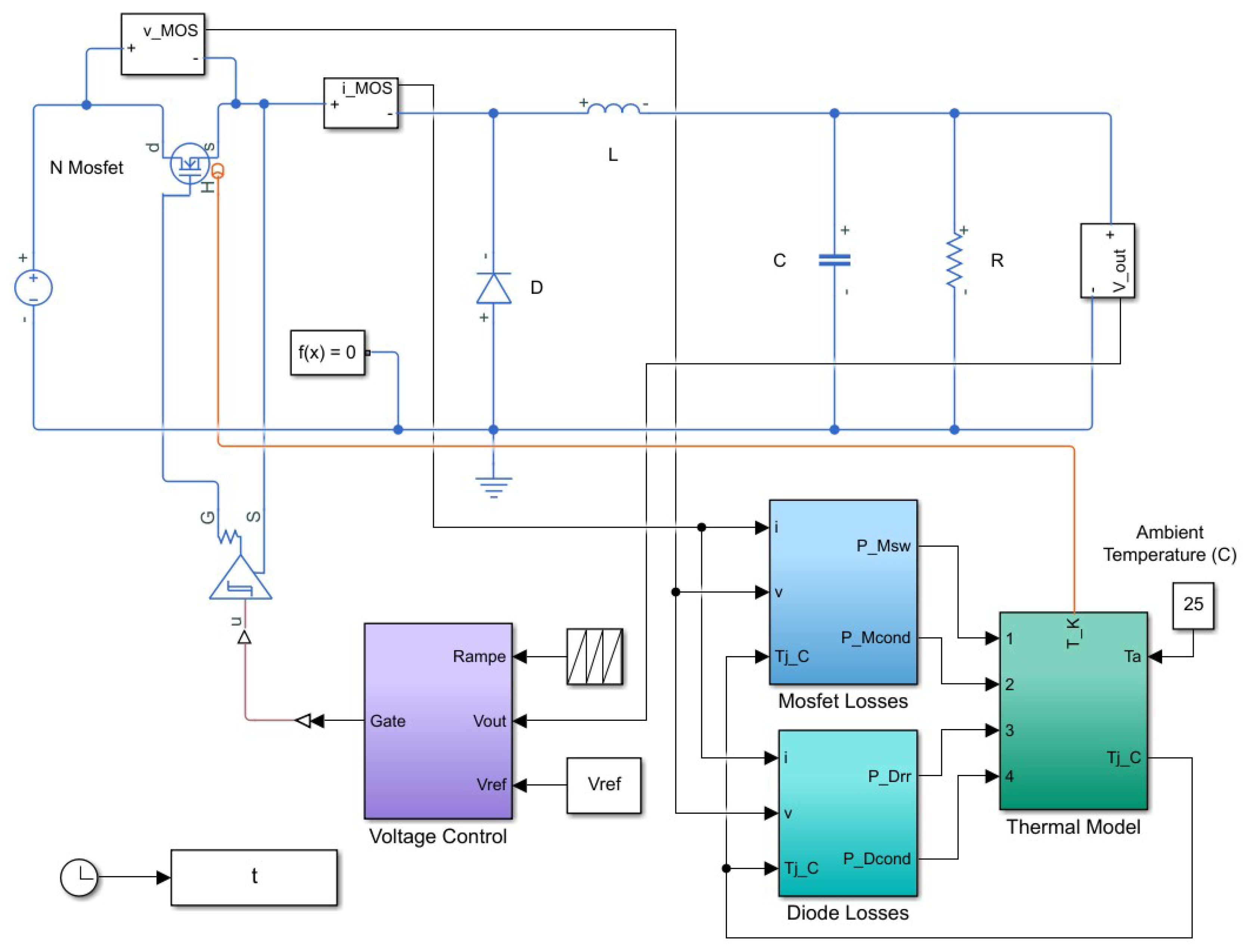
Figure 2.
Plots of (a) and (b) Mosfet current with a stable period-1T operation (f = 10 kHz).
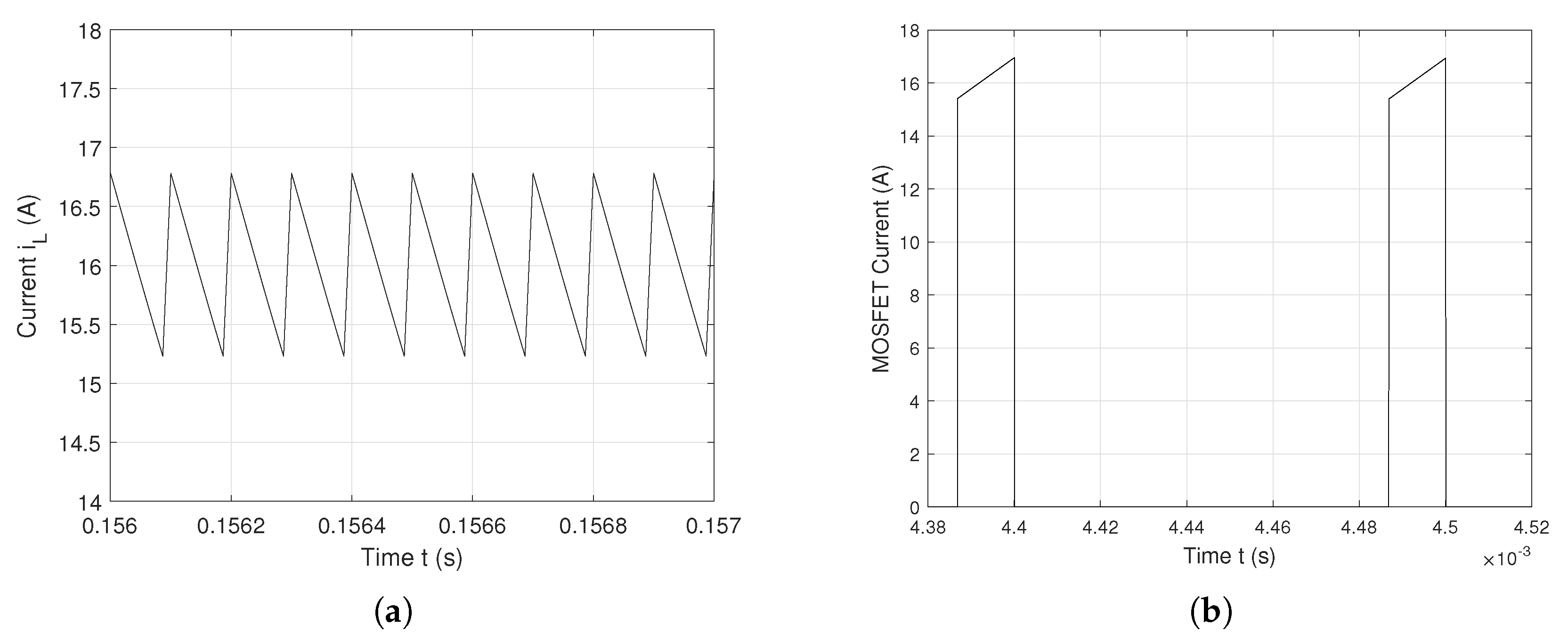
Figure 3.
Output voltage with a periodic behavior (f = 10 kHz); (b) Power spectrum of .
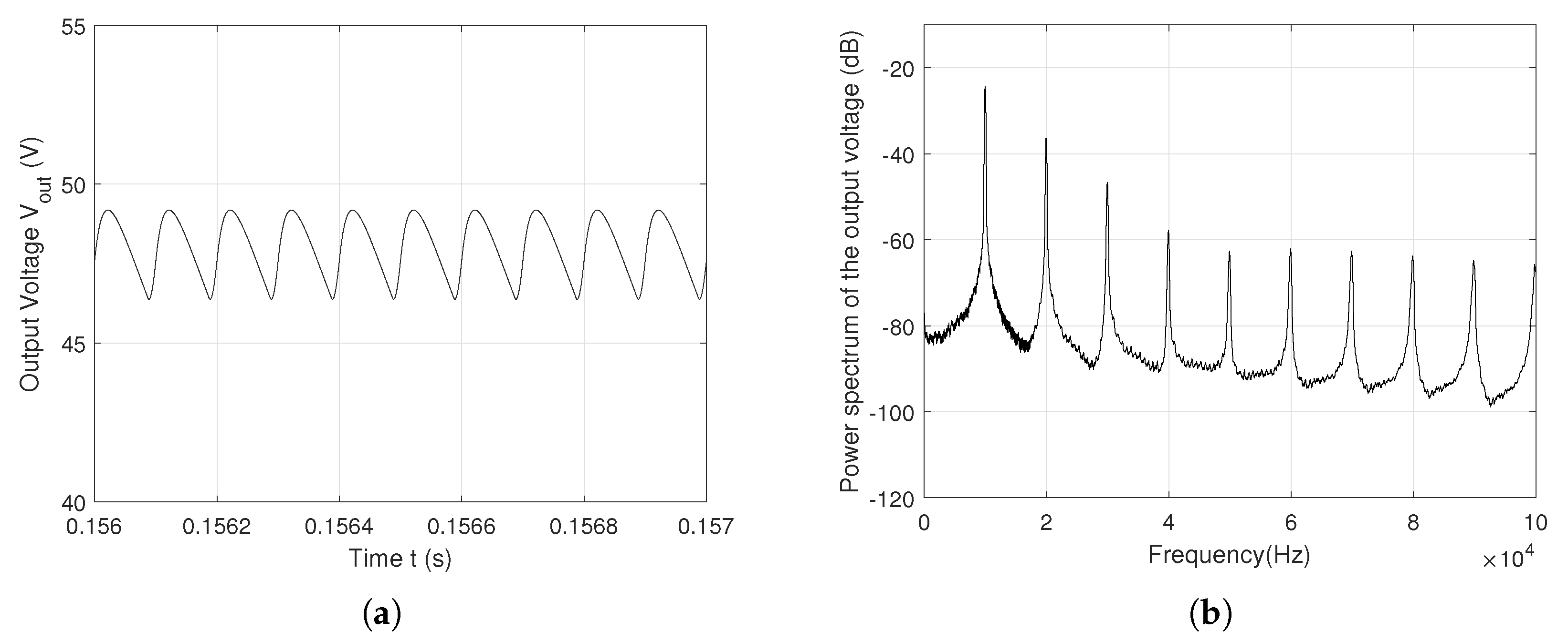
Figure 4.
Plots of (a) and (b) Mosfet current with a chaotic behavior (f = 10 kHz).
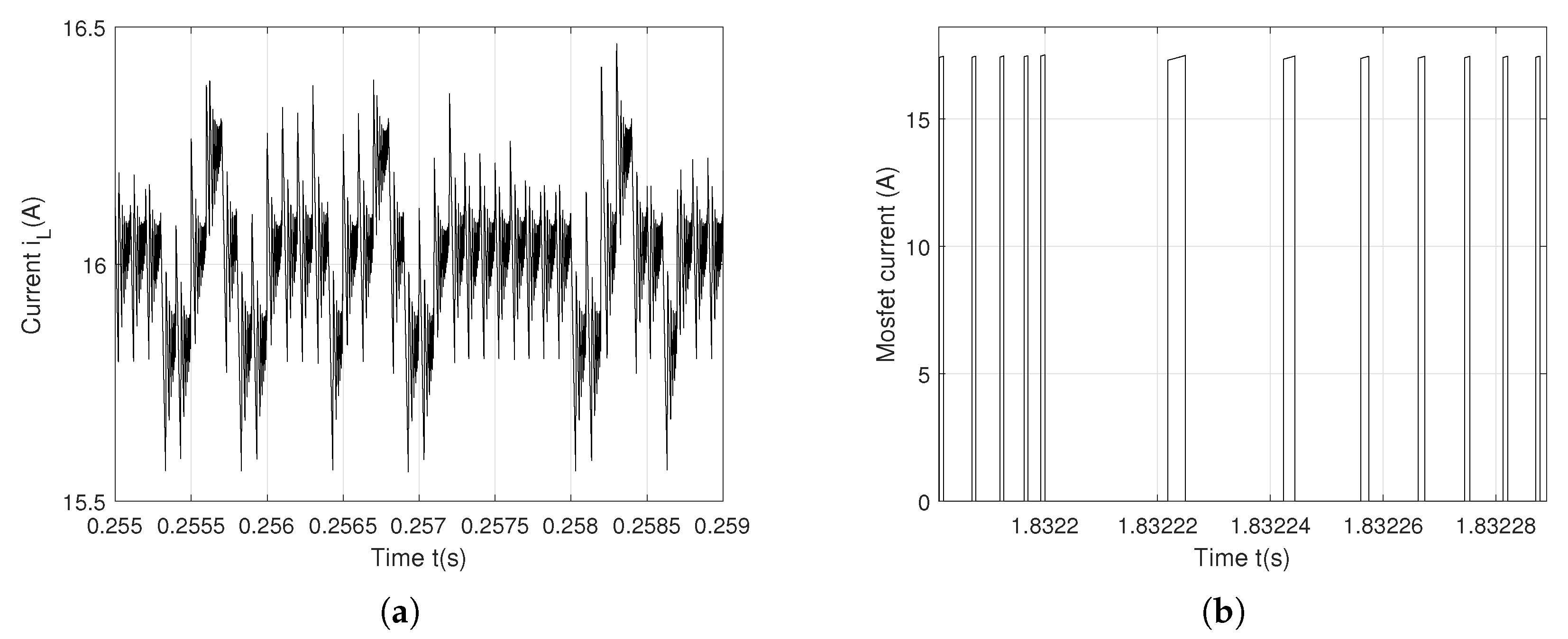
Figure 5.
(a) Output voltage with a chaotic behavior (f = 10 kHz); (b) Power spectrum of .
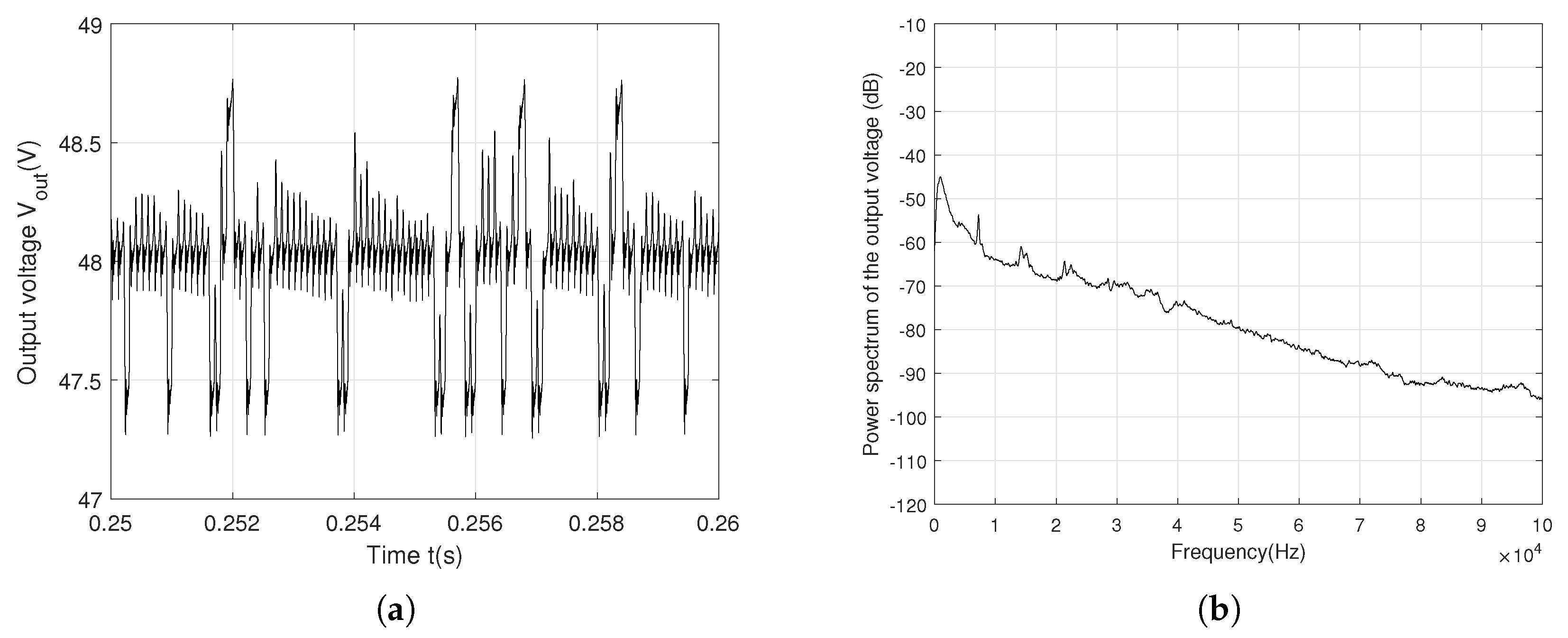
Figure 6.
(a) Output voltage with a periodic behavior (f = 20 kHz); (b) Power spectrum of .
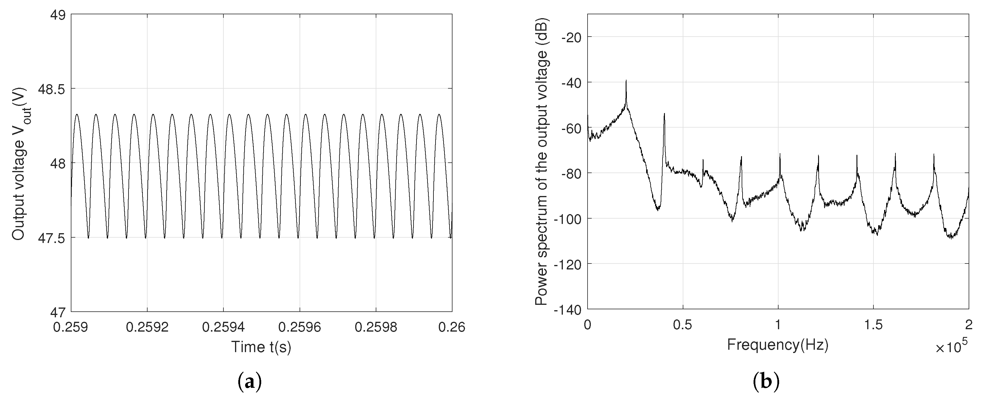
Figure 7.
(a) Output voltage with a chaotic behavior (f = 20 kHz); (b) Power spectrum of .
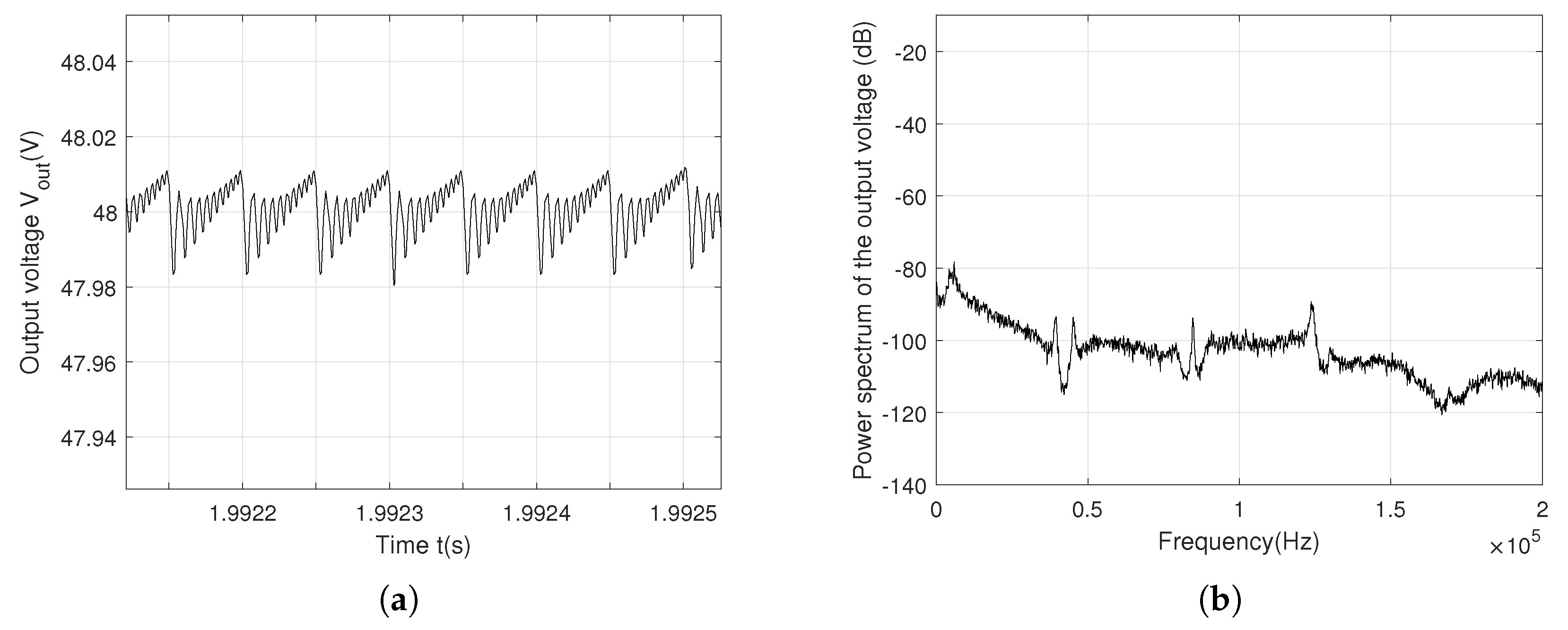
Figure 8.
(a) Output voltage with a periodic behavior (f = 50 kHz); (b) Power spectrum of .
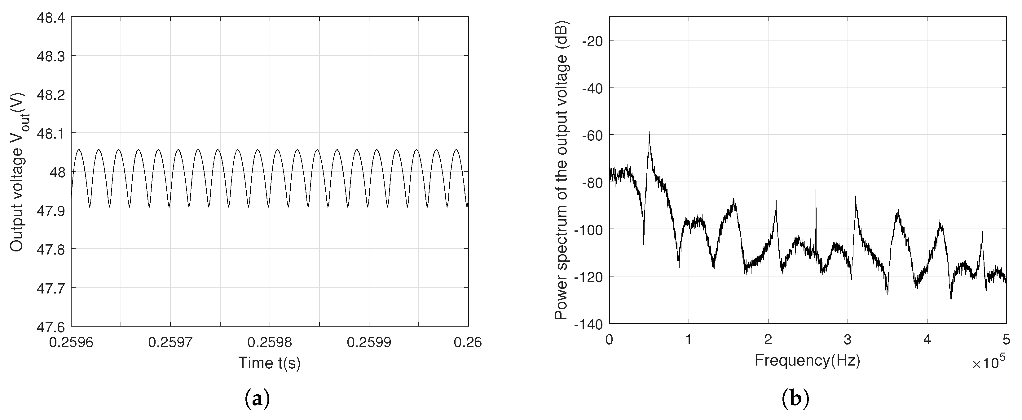
Figure 9.
(a) Output voltage with a chaotic behavior (f = 50 kHz); (b) Power spectrum of .
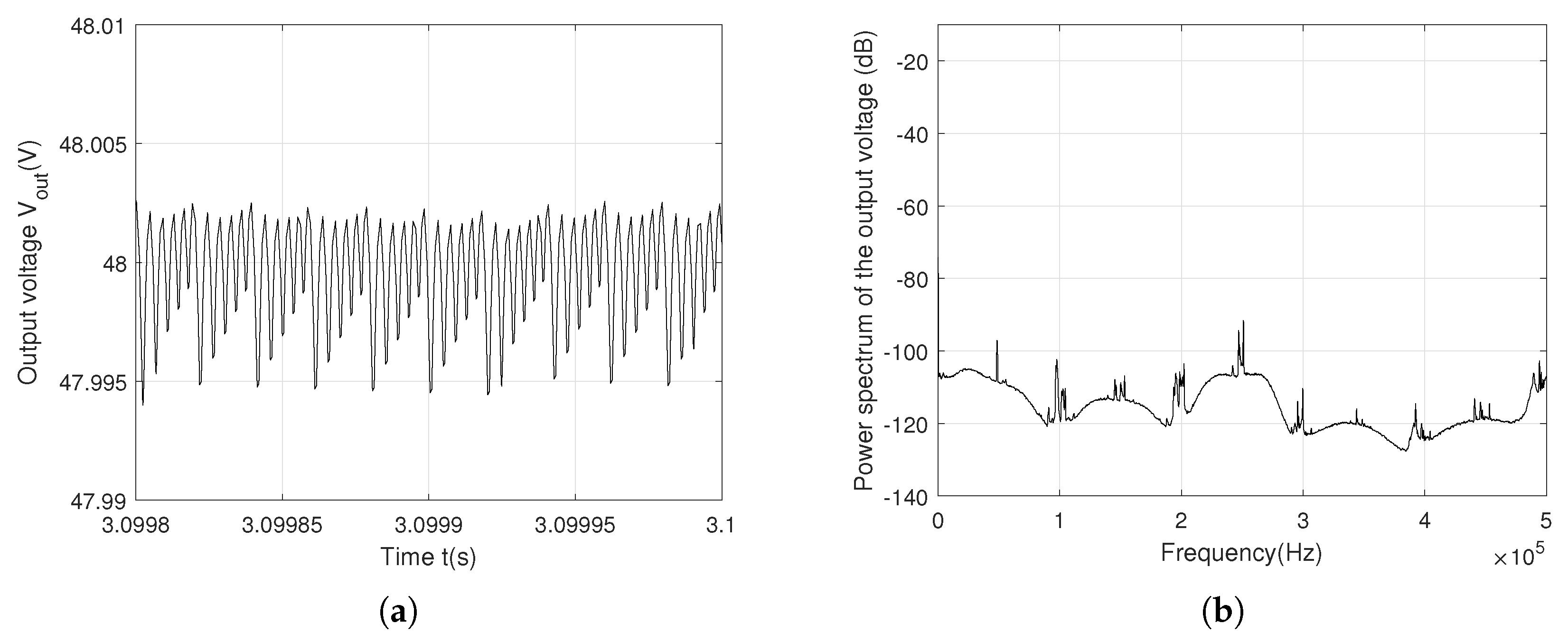
Figure 10.
Fitting curves of the static current–voltage characteristics - at C and C; (b) Mosfet energy power losses in function of the drain-source current , with = 800 V.
Figure 10.
Fitting curves of the static current–voltage characteristics - at C and C; (b) Mosfet energy power losses in function of the drain-source current , with = 800 V.
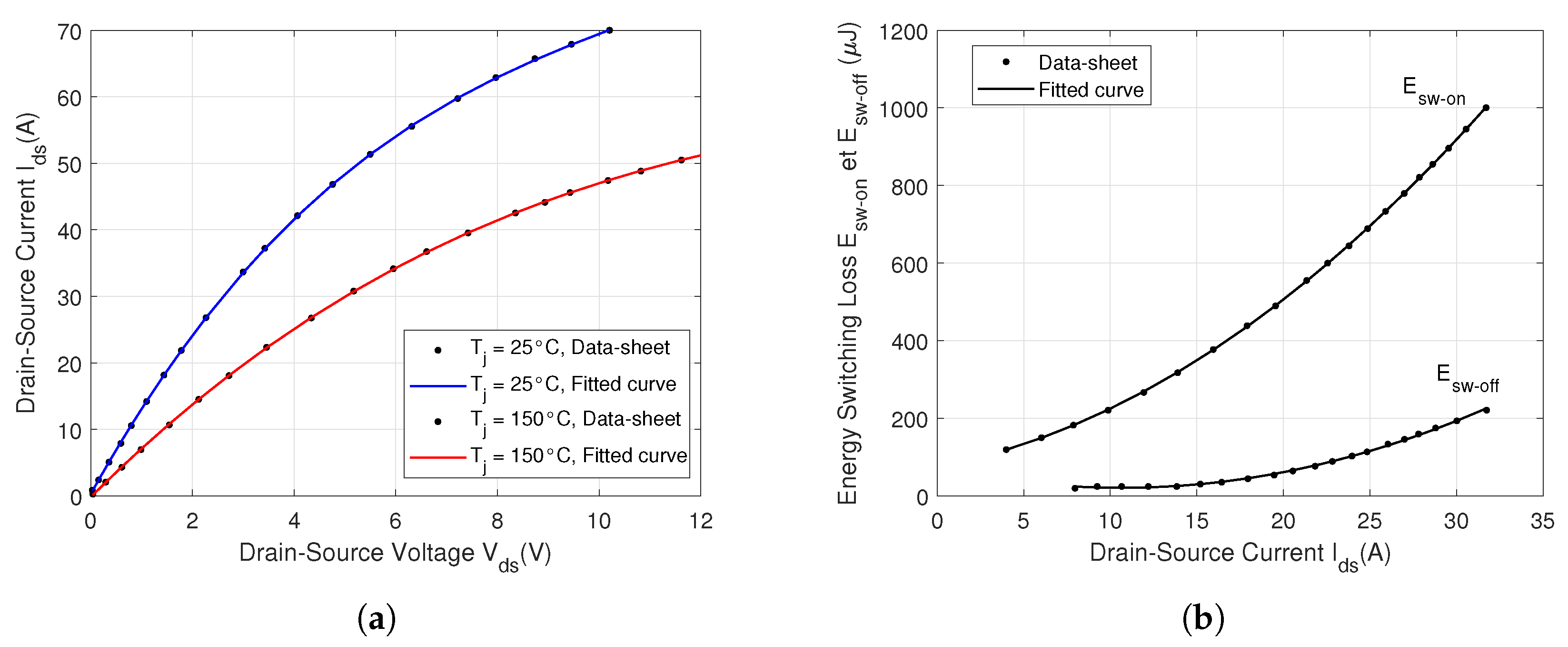
Figure 11.
Diode characteristics at = C and = C.
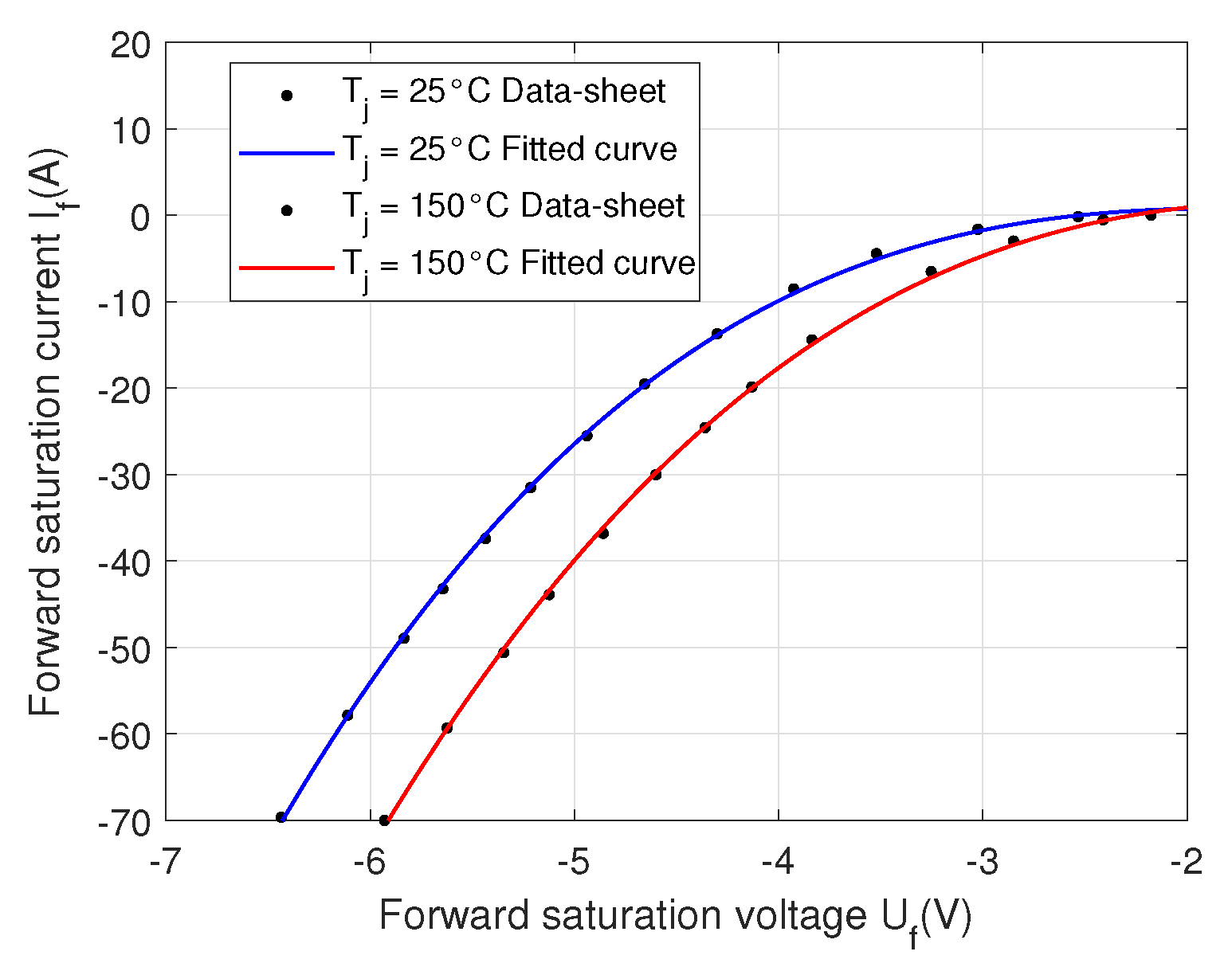
Figure 12.
(a) Comparison between the transient thermal impedance curves obtained through simulation and those provided in the datasheet; (b) Simulink model of the Foster network.
Figure 12.
(a) Comparison between the transient thermal impedance curves obtained through simulation and those provided in the datasheet; (b) Simulink model of the Foster network.
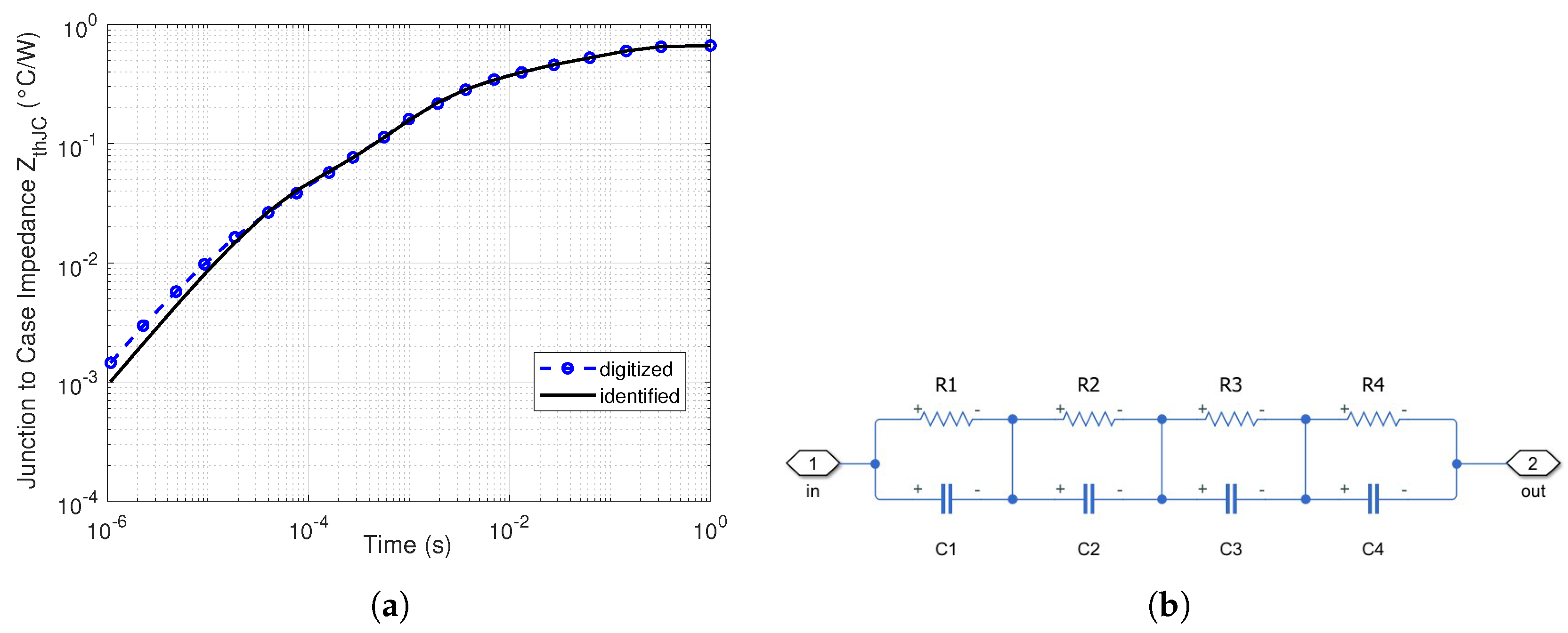
Figure 13.
Junction temperature with the switching frequency f = 10 kHz: (a) Periodic behavior using the controller (1); (b) Chaotic behavior using the controller (2).
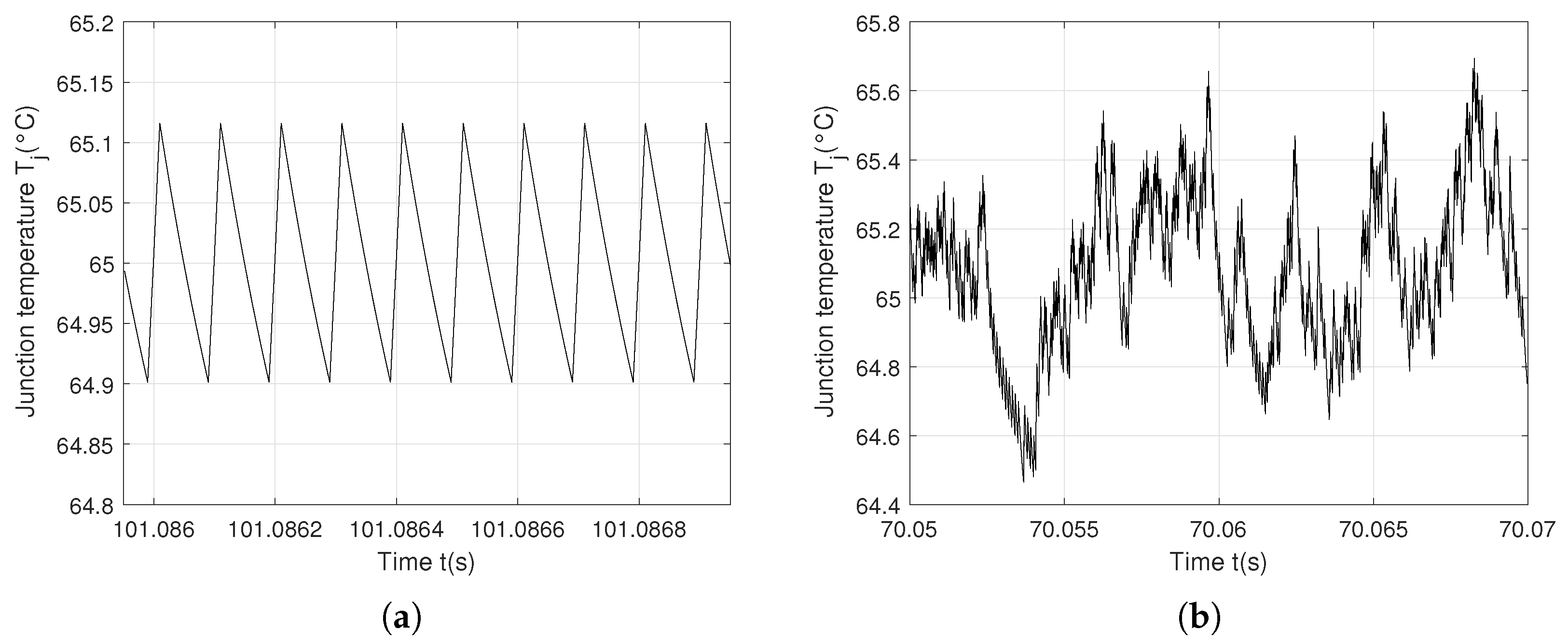
Figure 14.
Junction temperature with the switching frequency f = 20 kHz: (a) Periodic behavior using the controller (1); (b) Chaotic behavior using the controller (2).
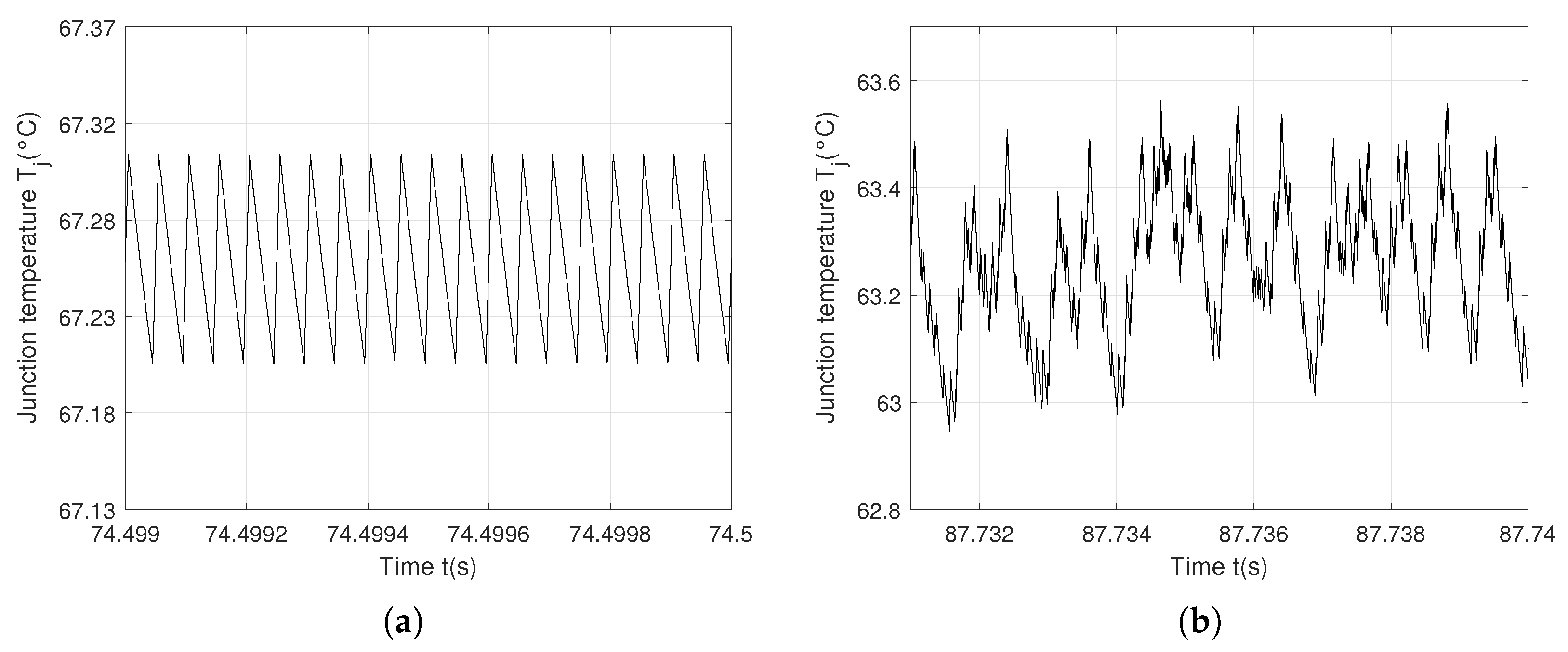
Figure 15.
Junction temperature with the switching frequency f = 50 kHz: (a) Periodic behavior using the controller (1); (b) Chaotic behavior using the controller (2).
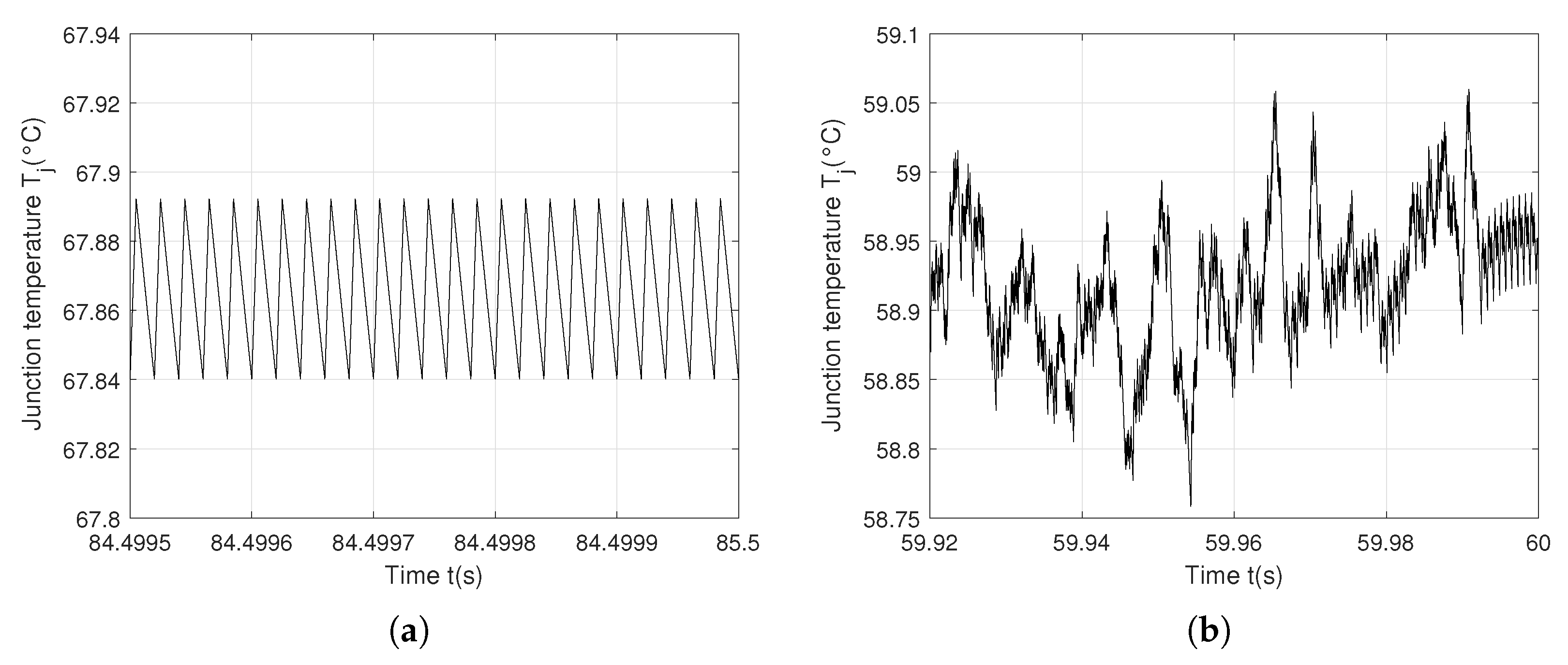
Figure 16.
(a) Thermal cycles considering and for a periodic behavior; (b) Thermal cycles considering and for a chaotic behavior obtained with the rainflow counting algorithm.
Figure 16.
(a) Thermal cycles considering and for a periodic behavior; (b) Thermal cycles considering and for a chaotic behavior obtained with the rainflow counting algorithm.
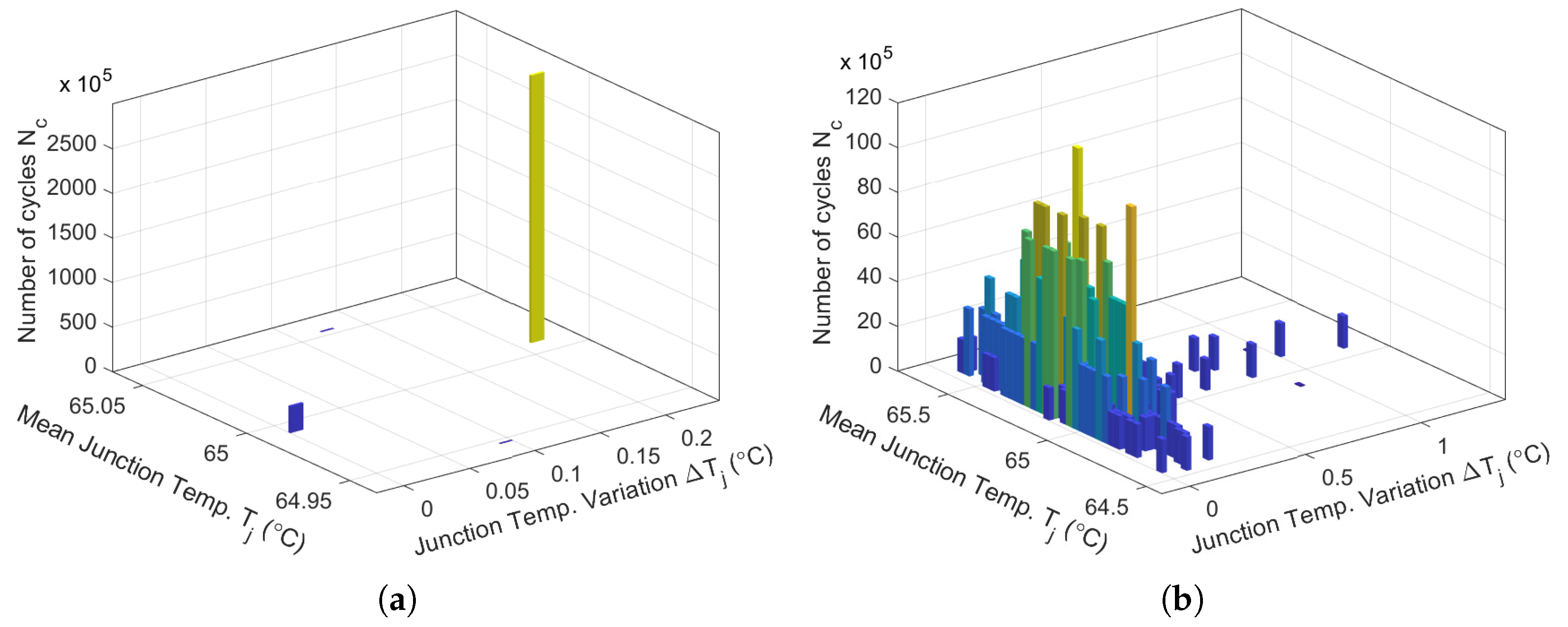
Figure 17.
(a) Thermal cycles considering and for a stable period-1T behavior; (b) Thermal cycles considering and for a chaotic behavior obtained with the rainflow counting algorithm.
Figure 17.
(a) Thermal cycles considering and for a stable period-1T behavior; (b) Thermal cycles considering and for a chaotic behavior obtained with the rainflow counting algorithm.
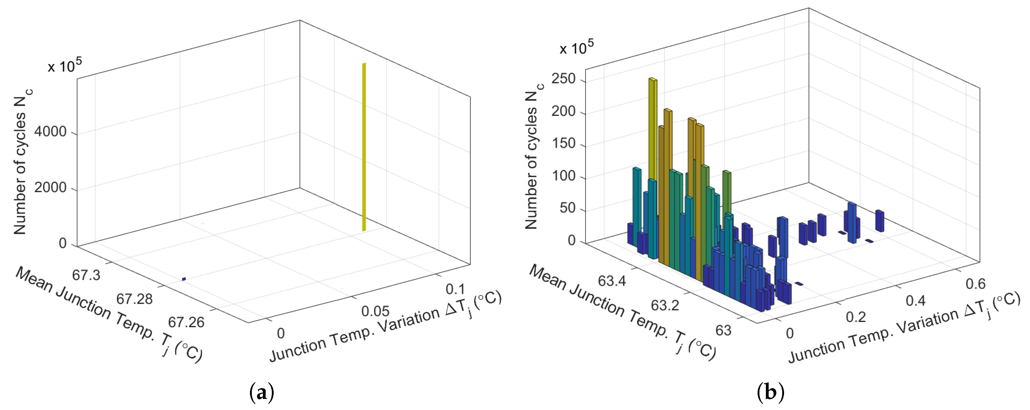
Figure 18.
(a) Thermal cycles considering and for a periodic behavior; (b) Thermal cycles considering and for a chaotic behavior obtained with the rainflow counting algorithm.
Figure 18.
(a) Thermal cycles considering and for a periodic behavior; (b) Thermal cycles considering and for a chaotic behavior obtained with the rainflow counting algorithm.
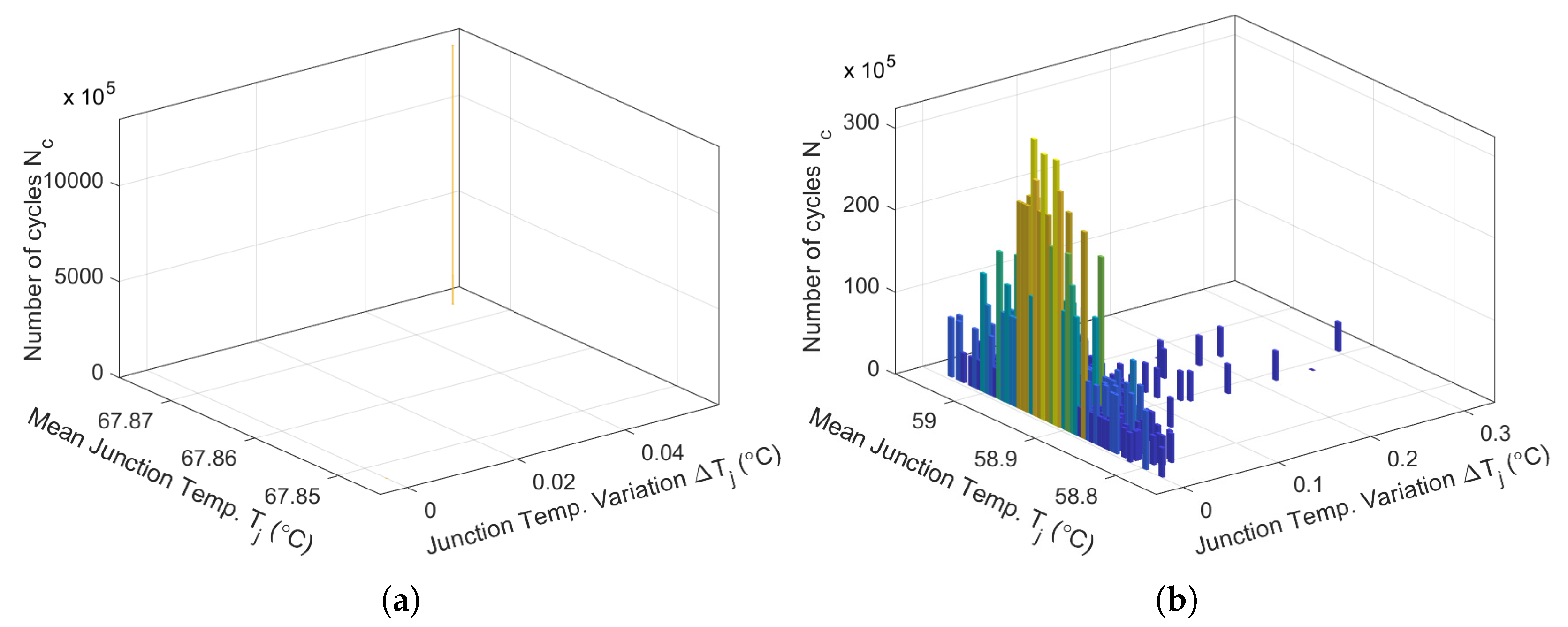

Table 1.
Ripple and maximum of power spectrum results for the study cases.
| Behavior | Controller | Switching frequency | Ripple | Maximum of power spectrum |
|---|---|---|---|---|
| 10kHz | 2.5 V | -25 dB | ||
| Stable 1T-period | PID | 20kHz | 0.8 V | -44 dB |
| 50kHz | 0.15 V | -60 dB | ||
| 10kHz | 1.8 V | -45 dB | ||
| Chaotic behavior | Anticontrol of chaos + PID | 20kHz | 0.025 V | -79 dB |
| 50kHz | 0.0075 V | -98 dB |
Table 2.
Accumulated fatigue results for the study cases.
| Behavior | Switching frequency | Mean of | Variation | Number of cycles | Accumulated fatigue |
|---|---|---|---|---|---|
| 10kHz | C | 0.C | 7.% | ||
| Periodic behavior | 20kHz | 67.C | 0.C | 4.% | |
| 50kHz | 67.C | 0.C | 6.% | ||
| 10kHz | 65.C | 1.C | 4.% | ||
| Chaotic behavior | 20kHz | 63.C | 0.C | 4.% | |
| 50kHz | 58.C | 0.C | 2.% |
Disclaimer/Publisher’s Note: The statements, opinions and data contained in all publications are solely those of the individual author(s) and contributor(s) and not of MDPI and/or the editor(s). MDPI and/or the editor(s) disclaim responsibility for any injury to people or property resulting from any ideas, methods, instructions or products referred to in the content. |
© 2025 by the authors. Licensee MDPI, Basel, Switzerland. This article is an open access article distributed under the terms and conditions of the Creative Commons Attribution (CC BY) license (http://creativecommons.org/licenses/by/4.0/).
Copyright: This open access article is published under a Creative Commons CC BY 4.0 license, which permit the free download, distribution, and reuse, provided that the author and preprint are cited in any reuse.


