
Submitted:
20 January 2025
Posted:
21 January 2025
You are already at the latest version
Abstract
In this work, we demonstrate an advanced light management strategy for bifacial perovskite solar cells by incorporating a silica-based anti-dust and anti-reflection (AR) coating. The silica layer provides dual functionality: enhancing optical efficiency through effective reflection suppression and protecting the solar cell surface from environmental contaminants, especially dust. The hydrophobic nature of the silica coating further prevents dust and particulate accumulation, supporting a self-cleaning mechanism that maintains cell transparency and performance over extended periods. The simulation results indicate that transitioning from a monofacial to a bifacial design with a silica layer on top has a considerable impact on PSC performance. The optimized bifacial structure demonstrates high-performance metrics, achieving a voltage of 1.35 V, a fill factor of 84.24 %, a current density (JSC) of 29.10 mA/cm², and a power conversion efficiency of 31.00 % when illuminated from the electron transport layer side. When illuminated from the hole transport layer side, the structure attains a PCE of 22.00 %, with a calculated bifaciality factor (BF) of 72.12 %, highlighting the potential through bifacial PSC design. Our findings reveal that the addition of the silica layer leads to a notable improvement in light harvesting efficiency.
Keywords:
Bifacial solar cell
; perovskite solar cells
; SCAPS-1D
; silica layer
; anti-dust and anti-reflection coatings
1. Introduction
In recent years, perovskite solar cells (PSCs) have attracted a lot of interest in solar cell research because of their quick development and potential for efficiency and cost-effectiveness. The first PSC in 2009 had a moderate efficiency of 3.8% [1,2]. But in just ten years, PSC efficiency for Methyl Ammonium Lead Halide (CH3NH3PbI3) perovskite-based cells [3] reached to 23.7%. Perovskite materials' better absorption coefficient, less binding energy, carrier mobility and diffusion length [4] make them suitable for photovoltaic applications. However, it's crucial to understand that certain lead-containing perovskite compounds, like MAPbI3, raise concerns regarding stability and environmental impact, which may limit their widespread application in solar cell technology. One solution to this problem is the creation of a bifacial structure, which makes use of superior optoelectronic properties such as higher carrier transport, improved absorption efficiency, and a lower exciton binding energy [5]. Featuring a 1.3 eV direct bandgap, this bifacial design excels in absorption and belongs to a periodic table group with similar properties to its lead-based counterpart. A transparent glass substrate, contact electrodes, perovskite layer, hole transport layer and electron transport layer make up the standard PSC structure, which is depicted in Figure 1. The bifacial structure of perovskite solar cells, when combined with a silica (SiO₂) layer on the front surface, enhances both the efficiency and durability of the cell. In a bifacial perovskite solar cell, light can enter from both the front and back sides, allowing for additional light capture and energy generation by utilizing light reflected from surrounding surfaces. The integration of a SiO₂ layer on the front surface serves as an anti-reflective coating, reducing incident light reflection and increasing light transmission into the active layers. This silica layer also acts as a protective barrier, improving the cell's stability by shielding the perovskite layer from environmental factors like moisture, UV exposure, and airborne particles. By reducing surface reflections, the SiO₂ layer ensures that a greater proportion of incoming light is absorbed by the perovskite layer, boosting the overall power conversion efficiency (PCE) and the short-circuit current density (Jsc) of the cell. By enhancing front-side light capture, the bifacial design maximizes performance under diffused and reflected light conditions, making it particularly advantageous in varied environmental conditions. Together, the bifacial architecture and the SiO₂ anti-reflective layer contribute to a highly efficient and stable perovskite solar cell, suitable for both rooftop installations and integrated photovoltaic applications where maximum light utilization is essential.
The electron transport layer(ETL) works as a hole-blocking layer [6], which helps prevent charge recombination. Titanium dioxide (TiO₂) is id favorable due to its transport mobility, stability, bandgap alignment, and adaptability to various deposition methods [7]. The hole transport layer(HTL), on the other hand, functions as an electron-blocking layer that prevents electron flow while encouraging hole transport [8]. Perovskite solar cells are becoming more and more necessary for vehicles as well as building integrated photovoltaics. Conventional or tandem structures are becoming less common because of this demand. Adopting a bifacial design is becoming a more practical solution instead.
The critical factors impacting the PSCs performance are their ability to effectively manage incident light, allowing for maximum photon absorption while minimizing losses from reflection. Anti-reflective coatings (ARCs) have been extensively studied and used to reduce the reflectance at the surface of solar cells. Traditionally, magnesium fluoride (MgF2) has been employed as an ARC material in PSCs because of its low refractive index (~1.38) and wide spectral coverage, effectively reducing reflection losses across a broad range of wavelengths [9]. MgF2 coatings, typically implemented in simulations using SCAPS-1D, have demonstrated notable improvements in light management and device optimization, with recent studies showing PCEs of up to 21.62% for MgF2-coated perovskite structures [10]. Despite these successes, the optical properties of MgF2 are not ideally matched for all PSC materials, which has led to continued research into alternative ARCs that could provide superior light management.
Silicon dioxide (SiO2) has a refractive index of approximately 1.5, has recently emerged as a promising ARC candidate for PSC applications. Unlike MgF2, SiO2 offers better compatibility with certain perovskite layers and provides the potential for enhanced constructive and destructive interference, allowing for further optimization of light absorption [11]. SiO2 coatings can be engineered to achieve the ideal balance between reflection minimization and transmission optimization, particularly for specific wavelengths that are crucial for PSC operation. Additionally, the robustness and environmental stability of SiO2 provide significant advantages in maintaining device performance over time, especially under variable climatic conditions [12,13].
Previous studies have demonstrated that ARCs can significantly affect the efficiency of PSCs by reducing surface reflection and improving photon utilization [14]. However, most prior research, particularly those relying on SCAPS-1D simulations, assumed either zero reflectance or employed default settings that failed to accurately account for the wavelength-dependent nature of light interaction with the ARC layer [10]. Such oversimplifications often lead to discrepancies between simulated and experimental results, thereby limiting the accuracy of predictive models for PSC performance. This study aims to bridge that gap by implementing a wavelength-dependent reflectance model for SiO2 as an ARC in PSCs as shown in Figure1, specifically focusing on perovskite structures that have demonstrated compatibility with SiO2 coatings. The need to progress performance and stability in PSCs for applications like Building Integrated Photovoltaics (BIPV) and Vehicle Integrated Photovoltaics (VIPV) underscores that tandem or conventional structures need to be switched to the bifacial structure. By addressing stability and environmental issues and offering substitutes for conventional materials, the study investigates new materials such as copper oxide (Cu2O) as possible HTMs. We can learn more about the viability of this type of solar panel by combining them all to observe the perovskite solar panel's performance. By enabling the absorption of more photons, thick absorber layers improve light absorption. Nevertheless, carrier diffusion length increases leading to higher recombination rates and transit times due to charge extraction pathways not being optimized. Both efficiency of light absorption and charge extraction are impacted by the bifacial structure's design, which includes the configuration of layers and interfaces.
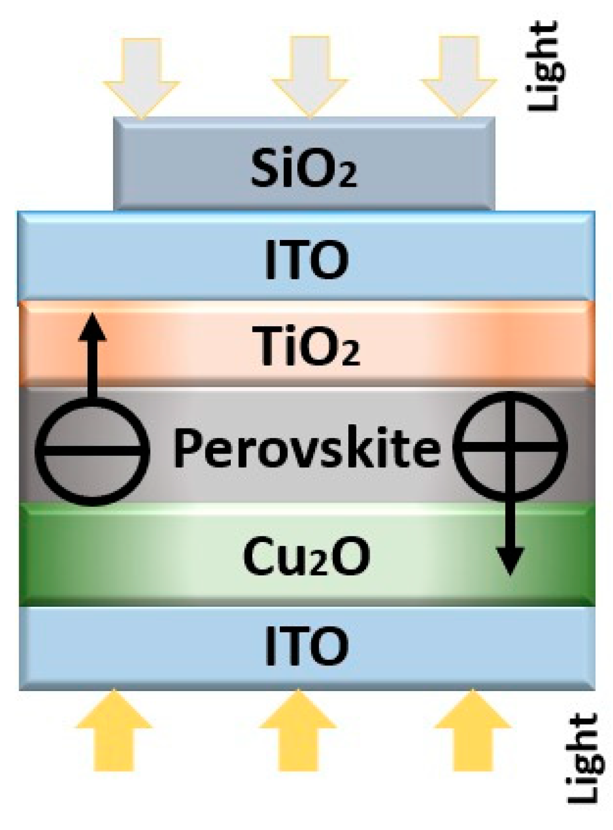
Figure 1.
SiO2/ITO/TiO2/perovskite/Cu2O/ITO device structure.
Prioritizing one component over another in design decisions can disturb the other, highlighting the need for careful optimization methods. By absorbing more sunlight, increasing light absorption usually results in a higher energy yield. Increasing charge extraction efficiency through modification by adding more contacts or layers, thereby compromising bifacial structure's visual transparency, particularly in building-integrated photovoltaics (BIPV). To guarantee commercial viability, trade-offs between pragmatic considerations and performance enhancements must be carefully assessed. Electrons can move around the device efficiently because metal oxides often have high electron mobility [3]. This improves overall device performance, reduces recombination losses, and expedites charge carrier extraction. Metal oxides' energy levels can be altered by dopants or compositional shifts to bring them into line with those of neighboring solar cell layers. This alignment lowers energy loss at interfaces and improves charge carrier extraction. Additionally, under normal operating conditions, metal oxides are typically chemically stable and do not degrade when exposed to light, oxygen, or moisture. This stability adds to the solar cell's long-term dependability and robustness.
Fluorine-doped tin oxide (FTO) and indium tin oxide (ITO) which are transparent conductive oxide have high optical transparency and electrical conductivity, Because of this combination, they can function as transparent conductive electrodes that effectively collect charge carriers while allowing light to pass through the active layer. Due to their affordability and abundance, metal oxides are desirable raw materials for solar cell manufacturing on a large scale. Their accessibility lowers total cost in producing solar panels, increasing the technology's economic feasibility. Metal oxides can perform a variety of tasks in a solar cell, including hole blocking, electron transport, and in some kinds of photovoltaic devices, active layer participation. Because of its adaptability, unique device architectures that meet particular performance requirements can be created. To get around these issues, this work explores the use of TiO2 as electron transport layer and Cu2O as hole transport layer in bifacial PSC. Numerous simulations are carried out with SCAPS, examining different parameters in each PSC layer and direct process of fabrication. For each layer to perform at its best (HTL, Abs, and ETL), critical parameters such as fill factor (FF), power conversion efficiency (PCE), open-circuit voltage (VOC), and short-circuit current (JSC) are analyzed. The study examines operating temperature, doping concentration, thickness, type, and defect density to identify the optimal configuration under SiO2 coating. Furthermore, PSC performance is examined under various incoming light concentrations through numerical analyses conducted with the SCAPS simulator in AM1.5G light conditions. The transmission option in SCAPS is used in these simulations to adjust the incoming light's intensity. By altering the transmission coefficient, this option enables the simulation of various light conditions.
2. Materials and Methods
SCAPS (Solar Cell Capacitance Simulator) is widely used for simulating the structural and material parameters impact in the perovskite solar cells (PSCs) performance. One key parameter studied through SCAPS is the effect of increasing the perovskite layer's thickness on overall device efficiency. As the thickness of the perovskite absorber layer increases, there is generally an initial improvement in the cell’s light absorption, which enhances the short-circuit current density (Jsc) due to the capture of more incident photons. This improvement, however, plateaus and may eventually reverse at higher thicknesses, where issues such as increased bulk recombination, longer carrier diffusion distances, and reduced charge extraction efficiency begin to offset the gains in light absorption. Excessive thickness can also lead to a drop in the open-circuit voltage (Voc), as charge carriers may recombine before reaching the respective electrodes. SCAPS simulations often reveal an optimal thickness range where the balance between light absorption and charge transport is maximized, resulting in peak power conversion efficiency (PCE). Through this approach, SCAPS allows for systematic exploration and optimization of PSC thickness to improve cell efficiency while avoiding material waste and ensuring practical manufacturability.
SCAPS-1D was developed in ELIS at University of Gent, was used in this work [15]. The software uses the continuity as well as Poisson equations (1).
where the G stands for generation rate, τn and τp for the electron and hole lifetimes, respectively. The diffusion coefficient and electron charge are D and q, respectively. The electrostatic potential is represented by Ψ, and the electron and hole mobilities are represented by μp and μn. Furthermore, concentrations of holes and free electrons where denoted by p(x) and m(x), whereas trapped holes and electrons are pt(x) and nt(x). The ionized acceptors and donors’ concentration is represented by N−D(x) and N+A(x), the electric field by ξ, and the direction along the thickness by x [16].
For this investigation, a conventional and optimized two-stage PSC model device structure with backlighting has been developed. The conventional device structure utilized in this work, ITO/Cu2O/Perovskite/TiO2/ITO/SiO2, is the initial stage to optimize PSC device structure. The optimization process primarily focused on the TiO2 layer while also examining other empirical properties such as operating temperature, layer thickness, and defects. Concurrent optimization of the perovskite layer, back contact layers, and hole transport layer involved examining different thicknesses.
Then, with dark currents present, the optimized structural design was investigated. The study also examined the doping and density of defects in the absorber layer affecting the PSC efficiency. 1.5G AM air mass illumination per square meter was used to run this simulation. In this study, each layer was optimized using PCE analysis of the PSC. The ETL optimization was the first step in the optimization process, which involved simulations with various thicknesses, defect densities and operating temperatures. After that, the absorber layer thickness was tuned, ranging from 100 to 1k nm. An optimized device structure was used to conduct and analyze dark current analysis, as shown in Figure 3. The impact of doping concentration and defect density on the recombination rate and performance of the absorber layer was also examined. Defect density and doping concentration in the absorber layer were altered from 1014 to 1018 cm-3, respectively. Enhancing solar cell’s reliability and efficiency requires an understanding of and ability to control defect density. Elevated defect densities may result in more charge carrier recombination, which would lower the device's overall efficiency.
Defects can also create trap states in the semiconductor's bandgap, which can impede the transport and collection of charge carriers and impair device performance even more. Researchers can evaluate the effects of various defect configurations on device performance by adjusting simulation parameters associated with defect density, such as defect energy levels or trap state concentrations. Fill factor, open-circuit voltage, and short-circuit current are the components of these variables. Researchers can also create passivation and defect mitigation strategies by examining the connection between device performance and defect density. Methods like material purification, surface passivation, and defect engineering can be beneficial leading to decrease in defect densities and raise solar cell efficiency and dependability. In conclusion, defect density is essential to comprehending and maximizing photovoltaic device performance. Researchers can learn more about how defects affect device behavior and create plans to lessen their effects by integrating defect density data into analyses and simulations, which will ultimately increase the reliability and efficiency of solar cells.
3. Results
3.1. Layer Thickness Optimization
Optimization of Layer thickness is covered in this section, with reference to hole transport layer and electron transport layer. The electron transport layer and hole transport layer layers thickness in the specific instance described are of 140 nm and 200 nm, in accordance with suggestions from previous research [1]. The simulation's operating parameters are displayed in Table 1.
The latter thickness was chosen for several reasons after it was discovered that a thickness of 500 nm had short-circuit current (JSC) and higher power conversion efficiency (PCE) than a thickness of 1000 nm. The active layer which was larger is used to maximize charge production and improve the device's light-absorbing capabilities, Performance gains diminish after this thickness because important parameters like short-circuit current become saturated. The relationship between absorber layer thickness and performance metrics is shown in Figure 2 and Figure 3.
Figure 2.
Performance variation in perovskite solar cell for the incident solar spectrum from the ETL side in the range of 100–20,000 nm of absorber layer thickness. The variables include (a) open circuit voltage (Voc), (b) short circuit current (Jsc), (c) fill factor (FF), and (d) efficiency.
Figure 2.
Performance variation in perovskite solar cell for the incident solar spectrum from the ETL side in the range of 100–20,000 nm of absorber layer thickness. The variables include (a) open circuit voltage (Voc), (b) short circuit current (Jsc), (c) fill factor (FF), and (d) efficiency.
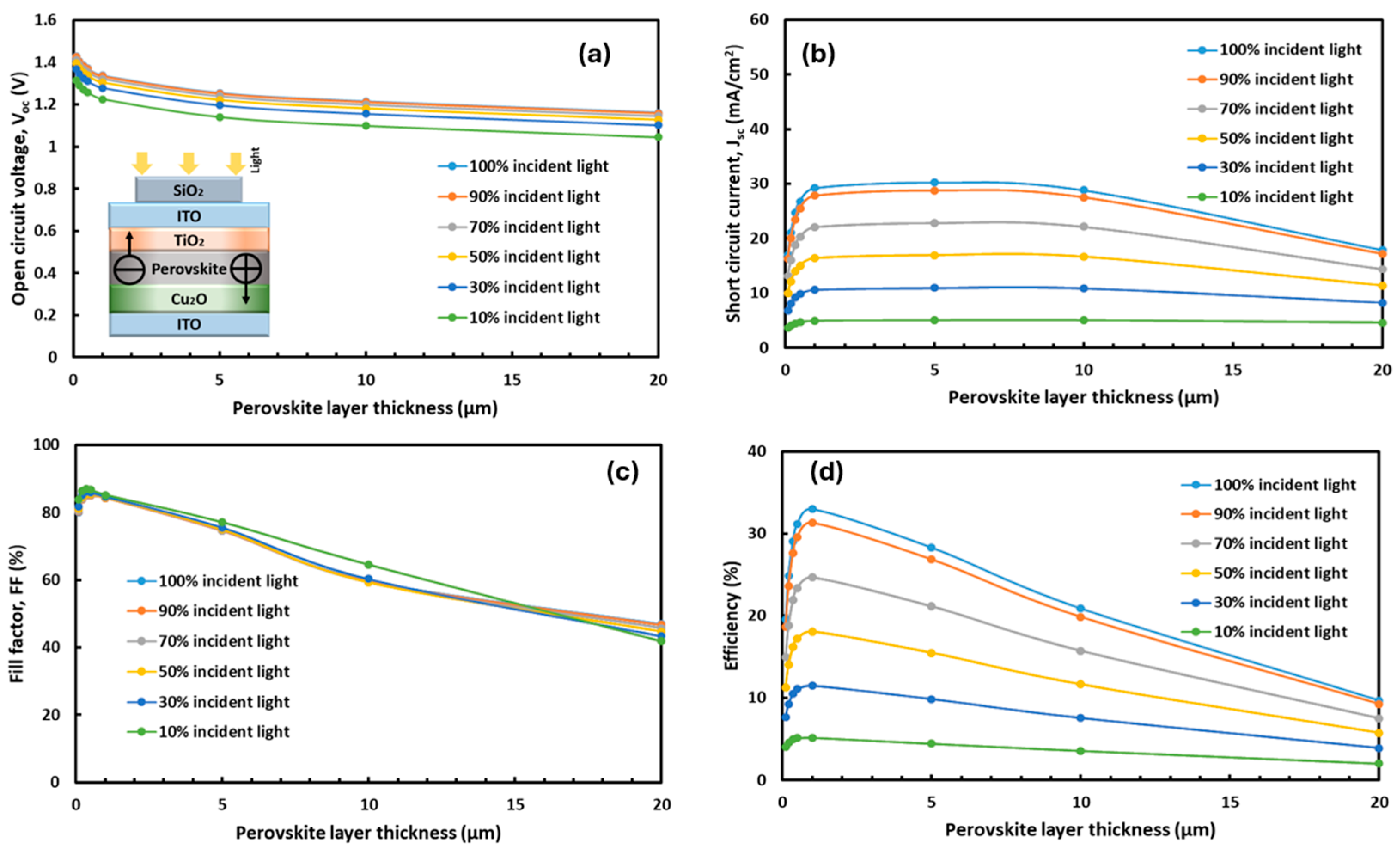
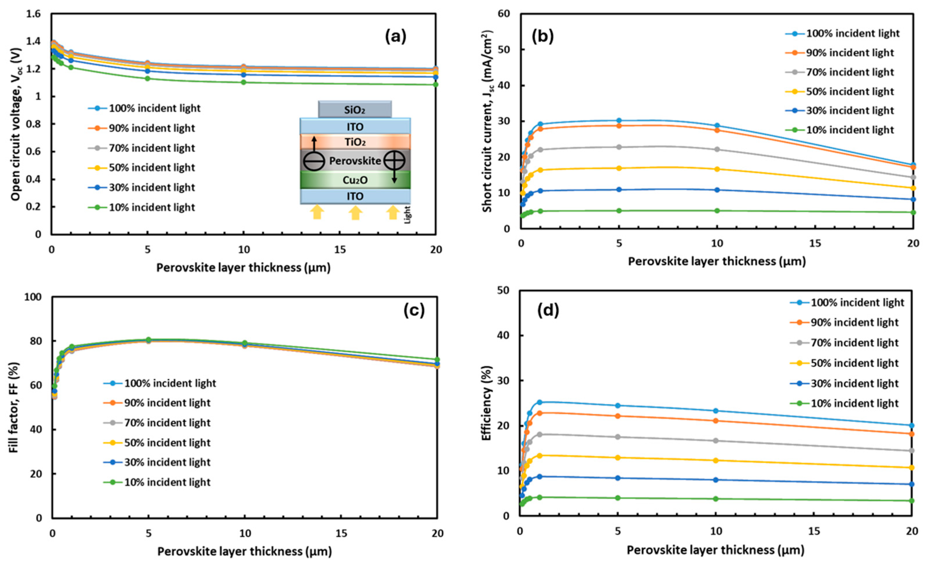
Figure 3.
Performance variation in perovskite solar cell for the incident solar spectrum from the HTL side in the range of 100–20,000 nm of absorber layer thickness. The variables include (a) open circuit voltage (Voc), (b) short circuit current (Jsc), (c) fill factor (FF), and (d) efficiency.
Figure 3.
Performance variation in perovskite solar cell for the incident solar spectrum from the HTL side in the range of 100–20,000 nm of absorber layer thickness. The variables include (a) open circuit voltage (Voc), (b) short circuit current (Jsc), (c) fill factor (FF), and (d) efficiency.
3.2. Effects of Operating Temperature on Bifacial Solar Cells
A comparative study on the bifacial perovskite solar cell with incident light from both the front and back sides to assess how performance is impacted, are shown in Figure 4 and Figure 5 was conducted. The operational temperature range considered for this analysis spanned from 300 K to 400 K. As the results indicate, a rise in operating temperature generally leads to a decline in cell efficiency. This is attributed to the temperature-dependent changes in key parameters such as carrier concentration, band gap, and electron and hole mobility, which tend to vary at elevated temperatures.
3.3. Effects of Doping Concentration on TiO2 Electron Transport Layer Layers
The bifacial solar cell performance was examined for various electron transport layer doping concentrations as shown in Figure 6.
4. Discussion
The above findings highlight the influence of layer thickness, operating temperature, and ETL doping concentration on the perovskite solar cells performance.
4.1. Layer Thickness Optimization
The analysis revealed that an absorber layer thickness of 500 nm yielded higher short-circuit current density (Jsc) and power conversion efficiency (PCE) compared to 1000 nm. Difficulties with defect management and material uniformity may be cause of the modest decline in efficiency seen beyond 1000 nm. It is important to keep in mind that, even though these ideal thickness values were demonstrated advantageous for conditions examined in this investigation, they may not be suitable for other configurations, and more investigation is needed to find out. We examined the effects of thickness in absorber layer, which ranges from 100 to 20,000 nm, on important factors influencing solar cell efficiency using SCAPS. Figure. 2 displays the when the thickness of the absorber layer increases, the short-circuit current increases as well, peaking at about 1000 nm and then plateauing in all cell types. After the incident photons are completely absorbed, the highest generated current is then generated, causing a slight drop (Figure. 2b). After eliminating defect-assisted carrier recombination, band-to-band recombination rate reduces performance beyond 1000 nm.
In this case the carrier densities under excitation are denoted by p and n., B is a constant unique to perovskites, and ni is the intrinsic density. We used the GaAs constant B (6.2× 10⁻¹⁰ cm−3.s−1), with 1.43 eV direct gap, because no measured value was available. The fill factor remains constant as the thickness increases above 1000 nm, but the PCE and Voc clearly decline as shown in Figure. 2d. These results imply that the thickness of the perovskite layer affects PSC performance. As the perovskite thickness exceeds 300 nm, the Voc sharply drops due to increased recombination, which leads to insufficient charge carrier separation at the interface between the absorber layer and the electron transport layer. This insufficient separation of charge carriers, which can also be brought on by higher series resistances, may cause Jsc to progressively drop. On the other hand, the TiO2 layer functions as both a hole-blocking and electrically conductive layer, while avoiding hole attachment which makes it easier to collect electrons in the absorber layer. Since the TiO2 layer is electrically conductive, its electrical conductivity is directly influenced by its thickness.
Increased photon absorption at the electron transport layer causes the electrical conductivity of growing TiO2 layer to drop, lowering PSC performance over time by raising the charge transfer resistance. We have kept the electron transport layer and hole transport layer at fixed thickness values due to considerations unique to the bifacial cell design. When B, the recombination constant is small, the saturation of both Jsc and Voc is visible beyond a thickness of 1000 nm, and when B is larger, it decreases, resulting in a subsequent saturation in PCE. Interestingly, the decline in Voc is more pronounced than the short circuit current for thicker perovskite layers. Understanding Voc's reliance on Jsc and the device's saturation current, J0, which is influenced by layer thickness, helps to understand this occurrence.
The device's dependence on its J0 saturation current is a main factor causing the open-circuit voltage (Voc) variation. Figure. 3c makes it evident that the fill factor (FF) remains relatively constant even when the absorber's thickness changes. Given that the incident light's fill factor from the electron transport layer side is comparable to that of other devices, the bifacial-based device's high VOC, and JSC could be the main factor contributing to its superior efficiency. According to calculations, changes in the solar cell layers' thickness have an impact on light transmission, which in turn affects bifaciality [17] [18]. A crucial statistic for describing bifacial solar cells is the bifaciality factor, which is the ratio of rear side's efficiency to the front side's efficiency. The module's minimal power output, measured in kilowatt peak (kWp), is divided by the surface area, measured in square meters (m²), to establish minimal efficiency.
4.2. Effects of Operating Temperature on Bifacial Solar Cells
The results in Figure 4 and 5 indicate the rise in operating temperature generally leads to a decline in cell efficiency. This is attributed to the temperature-dependent changes in key parameters such as carrier concentration, band gap, and electron and hole mobility, which tend to vary at elevated temperatures. Temperature-induced degradation in perovskite solar cells (PSCs) is a critical factor impacting device stability and performance, especially under prolonged exposure to sunlight. Elevated temperatures can lead to phase instability in the perovskite layer, accelerating decomposition and ion migration, which degrades cell efficiency over time. Incorporating a silica (SiO₂) anti-reflection coating (ARC) can help mitigate these effects. SiO₂, being thermally stable and possessing excellent optical properties, not only enhances light absorption by reducing reflection but also provides a protective layer that moderates the temperature rise within the PSC structure. This thermal buffering effect helps preserve the structural integrity of the perovskite layer by limiting direct thermal stress. Additionally, SiO₂’s hydrophobic nature provides a barrier against moisture ingress, which, in combination with temperature, often accelerates degradation. Studies have shown that PSCs with SiO₂ coatings maintain efficiency better than uncoated counterparts in high-temperature environments, highlighting SiO₂’s role as an effective ARC and stabilizer, contributing to the overall longevity and reliability of perovskite-based solar cells.
4.3. Effects of Doping Concentration on TiO2 Electron Transport Layer Layers
The perovskite absorber layer of 1000nm thickness was consistently associated with highest efficiency. While the fill factor remains constant, PCE and the open circuit voltage (Voc) both sharply decline when illuminated from the hole transport layer side as seen in Figure 6. Changes in doping concentration were crucial for controlling recombination and carrier transport, leading to notable variations in EQE, especially in transport layers like TiO2. When compared to experiments, simulations have certain limitations. Our simulations primarily offer insights into material properties, design parameters, and device performance prediction or optimization. To find out how different factors affect device performance, parameter sensitivity analysis can be done. This involves altering the geometry of the device, the material properties, the operating environment, or the fabrication parameters to pinpoint the main elements affecting performance. Additionally, simulations may reduce the necessity of iterative testing of the experiment which can help in design optimization and cost.
5. Conclusions
Our findings demonstrate that the efficiency of perovskite-based solar cells can be further boosted through a bifacial structure. If copper oxide's effectiveness as an HTM is confirmed by experiments, It's possible that the bifacial structure cell will perform even better. Furthermore, the device's longevity can be increased due to shielding perovskite from moisture. Initial numerical analysis using SCAPS-1D suggests the proposed structure could reach up to 31% power conversion efficiency (PCE). When illuminated from the p-side, efficiency increases by 22%, potentially achieving a total conversion efficiency of 33%. With material parameters taken from pertinent literature, the computed BF for this structure is 71%. Consequently, potential for developing functional n-i-p BPSCs is retained. It's worth noting, however, that much of our research remains theoretical, and further experimental work is needed to validate the effectiveness of our proposed improvements. Nonetheless, our study provides valuable new insights for developing perovskite-based solar cells that are more robust and efficient, potentially resulting in significant advancements in the renewable energy sector.
Author Contributions
KT: Writing – original draft, Methodology, Investigation, Data curation, Conceptualization; AR: Writing – original draft, Methodology, Investigation, Formal analysis, Data curation; AK: Investigation, Formal analysis; PC: Investigation, Formal analysis; BA: Investigation, Formal analysis; MIH: Investigation, Supervision, Formal analysis. All authors have read and agreed to the published version of the manuscript.
Funding
This research received no external funding.
Data Availability Statement
The data that supports the findings of this study are available from the corresponding author, M.I.H., upon reasonable request.
Conflicts of Interest
The authors declare no conflicts of interest.
References
- Grätzel, M. 2014. "The light and shade of perovskite solar cells." Nature Materials, 13: 838-842.
- Hossain, M. I., Tong, Y., Shetty, A., & Mansour, S. 2023. "Probing the degradation pathways in perovskite solar cells." Solar Energy, 265: 112128.
- M. I. Hossain, "E-beam evaporated hydrophobic metal oxide thin films as carrier transport materials for large scale perovskite solar cells.," Materials Technology, vol. 37, no. 4, pp. 248-259, 2022.
- Aïssa, B., Bufere, M., & Hossain, M. I. 2023. "Solar cell technologies." In Photovoltaic Technology for Hot and Arid Environments, Institution of Engineering and Technology, 59-109.
- Noorasid, N. S., et al. 2023. "Improved performance of lead-free perovskite solar cell incorporated with TiO₂ ELECTRON TRANSPORT LAYER and CuI HOLE TRANSPORT LAYER using SCAPs." Applied Physics, 129(2): 132.
- Liang, M., et al. 2020. "Improving stability of organometallic-halide perovskite solar cells using exfoliation two-dimensional molybdenum chalcogenides." npj 2D Materials and Applications, 4(1).
- Wang, E., Chen, P., Yin, X., Gao, B., & Que, W. 2018. "Boosting efficiency of planar heterojunction perovskite solar cells by a low temperature TiCl₄ treatment." Journal of Advanced Dielectrics, 8: 1850009.
- Ghosh, P., Sundaram, S., Nixon, T. P., & Krishnamurthy, S. 2021. "Influence of nanostructures in perovskite solar cells." Reference Module in Materials Science and Materials Engineering. Elsevier.
- Wang, D. L. 2016. "Highly efficient light management for perovskite solar cells." Scientific Reports, 6.
- Yoo, G. Y. 2020. "Broadband anti-reflective nanostructures by coating a low-index MgF₂ film onto a SiO₂ moth-eye nanopattern." ACS Applied Materials & Interfaces, 12.
- Zhao, P. 2018. "Device simulation of organic-inorganic halide perovskite/crystalline silicon four-terminal tandem solar cell with various antireflection materials." IEEE J. Photovoltaics.
- Arabatzis, I. 2018. "Photocatalytic, self-cleaning, anti-reflective coating for photovoltaic panels: characterization and monitoring in real conditions." Solar Energy.
- Hossain, M. I., Chelvanathan, P., Al Kubaisi, G., & Mansour, S. 2023. “Experimental and Numerical Study of Different Metal Contacts for Perovskite Solar Cells.” Cogent Engineering, 10(1): 2189502.
- Elumalai, N. K., & Uddin, A. 2016. "Hysteresis in organic-inorganic hybrid perovskite solar cells." Sol. Energy Mater. Sol. Cells.
- Lin, L., Jiang, L., Li, P., Fan, B., & Qiu, Y. 2019. "A modeled perovskite solar cell structure with a Cu2O hole-transporting layer enabling." J. Phys. Chem. Solids, 205-211.
- Mechole transport layery, E. A. 2002. "Properties of Materials." In Reference Data for Engineers. Elsevier.
- Song, Z., Li, C., Chen, L., & Yan, Y. 2022. “Perovskite Solar Cells Go Bifacial—Mutual Benefits for Efficiency and Durability.” Advanced Materials, 34(4): 2106805.
- Kumar, P., Shankar, G., & Pradhan, B. 2023. “Recent Progress in Bifacial Perovskite Solar Cells.” Applied Physics A, 129(1): 63.
- Afzaal, M., & Karkain, S. 2022. “Environmental Assessment of Perovskite Solar Cells.” In The Effects of Dust and Heat on Photovoltaic Modules: Impacts and Solutions, edited by A. Al-Ahmed et al., 279–289. Springer.
- Bal, S. S., Basak, A., & Singh, U. P. 2022. “Numerical Modeling and Performance Analysis of Sb-Based Tandem Solar Cell Structure Using SCAPS–1D.” Optical Materials, 127: 112282.
- Baloch, A. A. B., Hossain, M. I., Tabet, N., & Alharbi, F. H. 2018. “Practical Efficiency Limit of Methylammonium Lead Iodide Perovskite (CH₃NH₃PbI₃) Solar Cells.” Journal of Physical Chemistry Letters, 9(2): 426–434.
- Belarbi, M., Zeggai, O., & Louhibi-Fasla, S. 2022. “Numerical Study of Methylammonium Lead Iodide Perovskite Solar Cells Using SCAPS-1D Simulation Program.” Materials Today: Proceedings. [CrossRef]
- Hossain, Mohammad Istiaque, Brahim Aissa, Ayman Samara, Said A. Mansour, Cedric A. Broussillou, and Veronica Bermudez Benito. "Hydrophilic antireflection and antidust silica coatings." ACS omega 6, no. 8 (2021): 5276-5286.
- Hossain, M. I., Bousselham, A., Alharbi, F. H., & Tabet, N. 2017. “Computational Analysis of Temperature Effects on Solar Cell Efficiency.” Journal of Computational Electronics, 16: 776–786.
- Hossain, M. I., & Aïssa, B. 2017. “Effect of Structure, Temperature, and Metal Work Function on Performance of Organometallic Perovskite Solar Cells.” Journal of Electronic Materials, 46(3): 1806–1810.
- Khattak, Y. H., Vega, E., Baig, F., & Soucase, B. M. 2022. “Performance Investigation of Experimentally Fabricated Lead Iodide Perovskite Solar Cell via Numerical Analysis.” Materials Research Bulletin, 151: 111802.
- Michaelson, H. B. 1977. “The Work Function of the Elements and Its Periodicity.” Journal of Applied Physics, 48: 191911.
- Nath, B., Ramamurthy, P. C., Mahapatra, D. R., & Hegde, G. 2022. “Electrode Transport Layer-Metal Electrode Interface Morphology Tailoring for Enhancing the Performance of Perovskite Solar Cells.” ACS Applied Electronic Materials. [CrossRef]
- Nath, B., Ramamurthy, P. C., Hegde, G., & Mahapatra, D. R. 2022. “Role of Electrodes on Perovskite Solar Cells Performance: A Review.” ISSS Journal of Micro and Smart Systems. [CrossRef]
- Raza, E., et al. 2022. “Numerical Modeling and Performance Optimization of Carbon-Based Hole transport layer-Free Perovskite Solar Cells.” Optical Materials, 125: 112075.
- Saha, P., Halder, P., Singh, S., & Bhattacharya, S. 2024. “Optimization and Formulation of Different Hole-Transporting Materials (HTMs) for the Performance of Eco-Friendly Cs₂TiBr₆-Based Perovskite Solar Cells.” Energy Technology, 12(3): 2300991.
- Saha, P., Singh, S., & Bhattacharya, S. 2023. “Eco-Friendly Methyl-Ammonium Tin-Based Planar P–N Homojunction Perovskite Solar Cells: Design and Performance Estimation.” International Journal of Modern Physics B, 37(17): 22350169.
- Samantaray, M. R., Rana, N. K., Kumar, A., Ghosh, D. S., & Chander, N. 2022. “Stability Study of Large-Area Perovskite Solar Cells Fabricated with Copper as Low-Cost Metal Contact.” International Journal of Energy Research, 46(2): 1250–1262.
- Shiraishi, M., & Ata, M. 2001. “Work Function of Carbon Nanotubes.” Carbon, 39: 1913–17.
- Song, S. M., Park, J. K., Sul, O. J., & Cho, B. J. 2012. “Determination of Work Function of Graphene under a Metal Electrode and Its Role in Contact Resistance.” Nano Letters, 12: 3887–3892.
- Wang, M., et al. 2022. “Modular Perovskite Solar Cells with Cs₀.₀₅ (FA₀.₈₅MA₀.₁₅)₀.₉₅ Pb (I₀.₈₅Br₀.₁₅)₃ Light-Harvesting Layer and Graphene Electrode.” Journal of Electronic Materials, 51(5): 2381–2389.
- Wu, Y., et al. 2022. “Broad-Band-Enhanced Plasmonic Perovskite Solar Cells with Irregular Silver Nanomaterials.” ACS Applied Materials & Interfaces. [CrossRef]
Figure 4.
Performance of the device for the incident solar spectrum from the ETL side at different operating temperatures for the absorber layer thickness of 350 nm (a) Open circuit voltage (Voc), (b) short circuit current (Jsc), (c) fill factor (FF), and (d) efficiency of perovskite solar cells.
Figure 4.
Performance of the device for the incident solar spectrum from the ETL side at different operating temperatures for the absorber layer thickness of 350 nm (a) Open circuit voltage (Voc), (b) short circuit current (Jsc), (c) fill factor (FF), and (d) efficiency of perovskite solar cells.
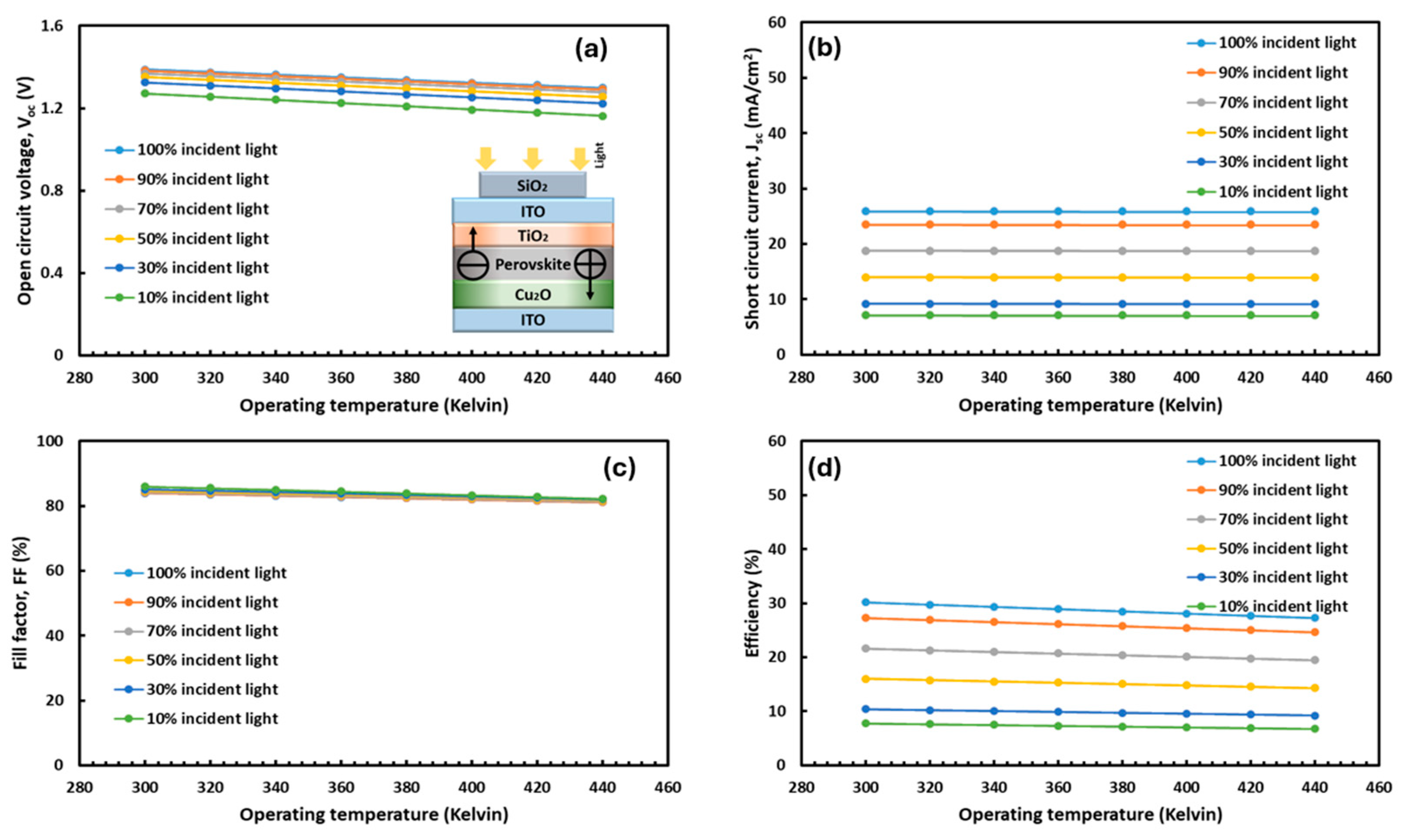
Figure 5.
Performance of the device for the incident solar spectrum from the ETL side at different operating temperatures for the absorber layer thickness of 350 nm (a) Open circuit voltage (Voc), (b) short circuit current (Jsc), (c) fill factor (FF), and (d) efficiency of perovskite solar cells.
Figure 5.
Performance of the device for the incident solar spectrum from the ETL side at different operating temperatures for the absorber layer thickness of 350 nm (a) Open circuit voltage (Voc), (b) short circuit current (Jsc), (c) fill factor (FF), and (d) efficiency of perovskite solar cells.
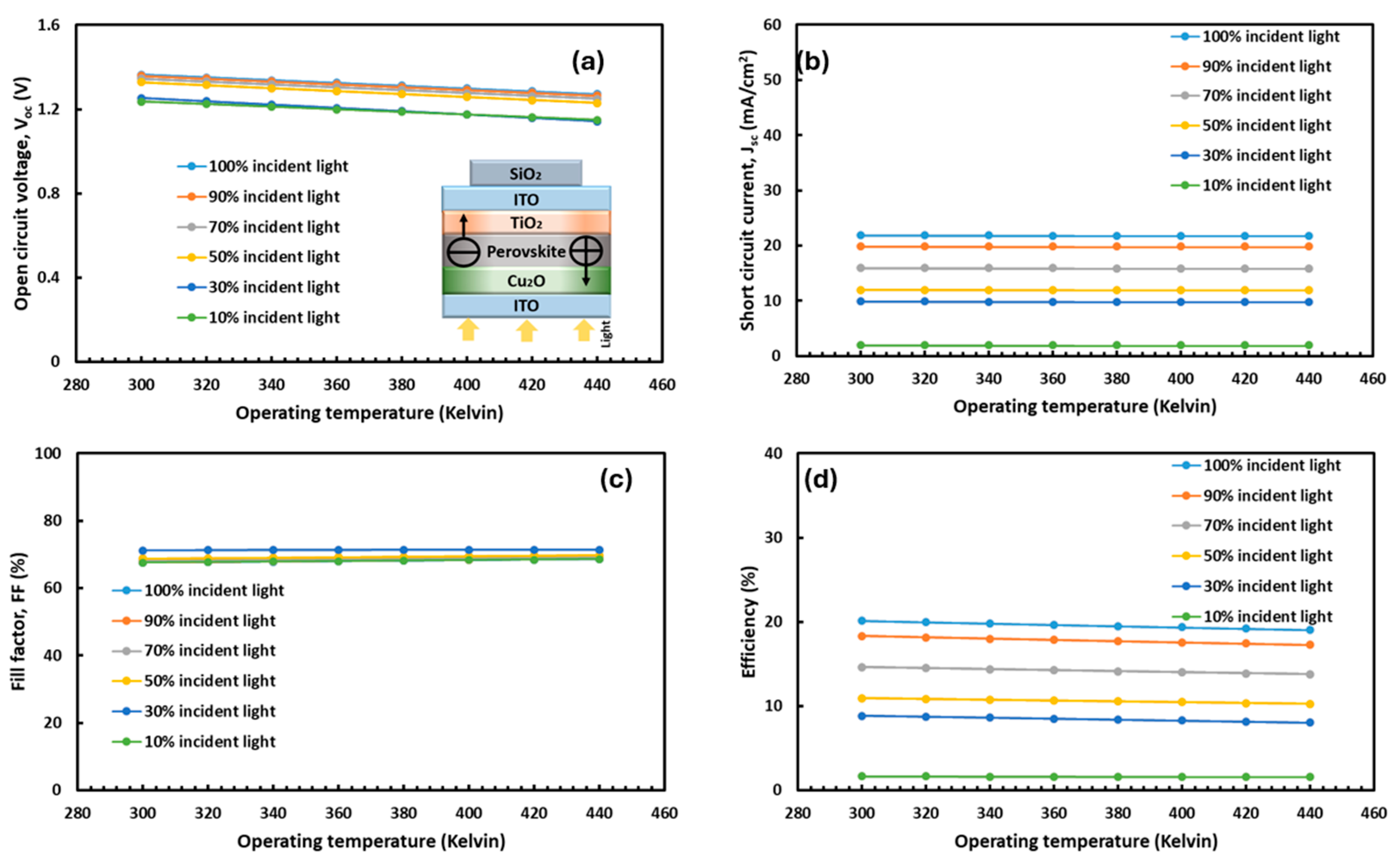
Figure 6.
Variations in the performance of solar cells within the absorber layer thickness range of 350 nm for different TiO2 ETL doping concentrations (a) Open circuit voltage (Voc), (b) Short circuit current (Jsc), (c) Fill factor (FF), and (d) Efficiency (η) of perovskite solar cells.
Figure 6.
Variations in the performance of solar cells within the absorber layer thickness range of 350 nm for different TiO2 ETL doping concentrations (a) Open circuit voltage (Voc), (b) Short circuit current (Jsc), (c) Fill factor (FF), and (d) Efficiency (η) of perovskite solar cells.
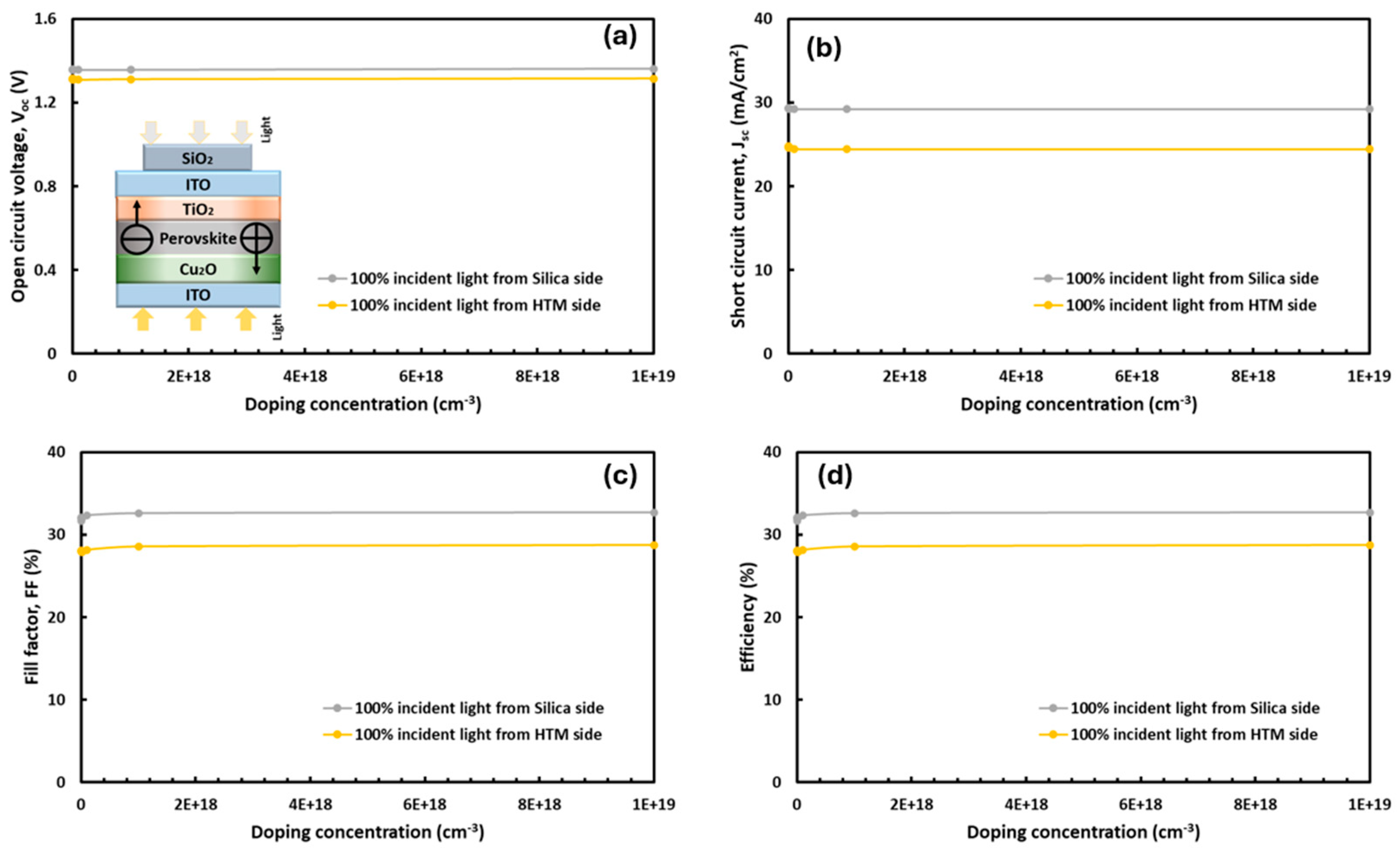

Table 1.
Used values to run the simulation.
| Parameters | Layer used | |||
|---|---|---|---|---|
| TiO2 | SiO2 | Cu2O | Perovskite | |
| Bandgap(eV) | 3.260 | 6.300 | 2.200 | 1.500 |
| Electron Thermal Velocity(cm/s) | 1.007E+7 | 1.007E+7 | 1.007E+7 | 1.007E+7 |
| Electron affinity(eV) | 4.000 | 3.200 | 3.200 | 3.900 |
| Dielectric permittivity | 10.000 | 3.900 | 9.400 | 10.000 |
| CB(1/cm3) | 2.00E+18 | 2.02E+17 | 8.00E+17 | 2.00E+18 |
| VB(1/cm3) | 1.80E+18 | 1.20E+19 | 1.80E+19 | 1.80E+18 |
| Electron Mobility(cm2/Vs) | 2.000E+2 | 6.250E+1 | 2.000E+2 | 2.000E+2 |
| Hole Thermal Velocity(cm/s) | 1.000E+2 | 1.000E+2 | 1.000E+7 | 1.000E+2 |
| Hole Mobility(cm2/Vs) | 2.500E+1 | 0.800 E+1 | 1.000E+2 | 1.000E+1 |
| CB(1/cm3) | 2.00E+18 | 2.02E+17 | 8.00E+17 | 2.00E+18 |
| VB(1/cm3) | 1.800E+18 | 1.10E+19 | 1.800E+19 | 1.800E+18 |
Disclaimer/Publisher’s Note: The statements, opinions and data contained in all publications are solely those of the individual author(s) and contributor(s) and not of MDPI and/or the editor(s). MDPI and/or the editor(s) disclaim responsibility for any injury to people or property resulting from any ideas, methods, instructions or products referred to in the content. |
© 2025 by the authors. Licensee MDPI, Basel, Switzerland. This article is an open access article distributed under the terms and conditions of the Creative Commons Attribution (CC BY) license (http://creativecommons.org/licenses/by/4.0/).
Copyright: This open access article is published under a Creative Commons CC BY 4.0 license, which permit the free download, distribution, and reuse, provided that the author and preprint are cited in any reuse.


