Submitted:
15 January 2025
Posted:
17 January 2025
You are already at the latest version
Abstract
As one of the most accurate instruments in history, the optical clock will be used as the measuring equipment for the next generation of seconds. The demand for miniaturization of optical clock is progressively urgent. In this paper, a multi-channel radio frequency module with a 20% volume of the commercial module is designed and implemented for the transportable 40Ca+ ion optical clock. Based on the double crystal oscillator interlocking technique,1 GHz low-phase noise reference source is developed for direct digital synthesis. By simulation and optimization of the signal link design, a frequency range of the low-phase noise RF signal can reach 0-400 MHz with a 4 μHz resolution. Through two-stage power amplified with different kinds of filters, it can get an output power up to +33 dBm (2 W) at 100 MHz with a 25 dBc/Hz phase noise lower than the commercial module at 1 Hz, and its third harmonic suppression ratio has been reduced by more than 20 dBm at the frequency point of 300 MHz. This multi-channel RF module is used for the power stability and timing control test of 729 nm clock laser, to meet the requirements of the transportable 40Ca+ optical clock. Without this, this module can also be applied to other quantum systems such as quantum absolute gravimeter, quantum gyro and quantum computer.
Keywords:
Transportable 40Ca+ ion optical clock
; Signal source
; Direct digital synthesis
; Power amplifier
1. Introduction
With the rapid development of laser cooling[1,2,3,4,5], ultra narrow linewidth laser[6,7,8,9] and femtosecond optical frequency comb[10,11], optical clock plays an important role in the measurement of basic physical constants[12], the verification of general relativity[13,14], gravitational wave measurement[15,16,17] and other precise measurement physics[18,19]. In recent years, with the increasingly urgent demand for the definition of the next generation second[20] and the measurement of the elevation difference[21,22], the miniaturization research of the key sensing components of the optical clock has been widely concerned[23,24]. The working process of optical clocks involves complex laser modulation technology, that radio frequency (RF) modules are indispensable to drive or modulate the acousto-optic modulators (AOMs) and electro-optic modulators (EOMs) in this process. Therefore, RF module stands as a key component of optical clock, and its miniaturization research is of great significance to meet the requirement of a transportable optical clock.
At present, the RF module in laboratory-based clock system is mainly provided in two ways: one is the combination of a commercial signal source and a commercial power amplifier module, which is used to provide RF driver. For example, in the 40Ca+ optical clock, the Innovation Academy for Precision Measurement Science and Technology (APM), Chinese Academy of Sciences (CAS) uses 5183B and direct digital synthesis (DDS) modules as the signal source[25]. Additionally, they use a commercial broadband power amplifier to amplify the signal source. Another way is the combination of self-developed signal source and commercial power amplifier module. For example, in the 9Be+ ion optical clock of University of Science and Technology of China, the self-developed 4-channel 2.8 Gsps@14-bit arbitrary waveform generator and 16-channel 1 Gsps@14-bit DDS module used as a signal source, then pass a commercial power amplifier as the RF driver, which can improve the integration of the system[26].
To further improve the integration of the system, we use a self-developed signal source and power amplifier as the RF driving module. The integration of the module is improved by mechanical-electrical joint design, which solves the size problem for integration in the transportable 40Ca+ optical clock system. Based on the double crystal oscillator interlocking technique, its output frequency range can reach 0-400 MHz with a 4 μHz resolution, and output power is up to +33 dBm. Finally, this module is tested by the 729 nm clock laser power stabilization and timing control, which can meats the requirement of the transportable 40Ca+ optical clock system.
The rest of this paper is as follows: Section 2 introduces the design method and key technology of integrated RF module and introduces the performance test results of the module, Section 3 introduces the experimental composition of RF module applied to 40Ca+optical clock and the test results of power stability and timing control of the 729 nm laser, and Section 4 is the conclusion.
2. Design of Integrated RF Source
The integrated RF source consists of two parts: a RF signal source and a power amplifier, which usually is used to drive or modulate the AOM and EOM in the laser path of a transportable 40Ca+ optical clock system. And its frequency and power can be changed in real time according to the time sequence requirements in the optical clock experiment process.
2.1. RF Signal Source
At present, the design methods of RF signal sources mainly include direct analog frequency synthesis (DAS), Phase Locked Loop (PLL) [27,28,29]and DDS[30,31]. In this design, the advantages of PLL and DDS are combined, and the mixed frequency synthesis technology of PLL+DDS is adopted. Firstly, PLL is used to double the 10 MHz signal to 1 GHz as the working clock of DDS, and then any frequency within 400 MHz is generated by DDS frequency division. The output frequency of the DDS can be expressed as
where FTW is the frequency control words, N is the number of bits in the DDS chip, and is the reference frequency. According to Nyquist’s sampling theorem, a unique analog signal can be obtained only when the sampling signal frequency is more than twice the signal frequency; theoretically, the maximum output frequency of the DDS is half of its input frequency. However, due to the digital characteristics and process effects of the DDS chip, the actual maximum output frequency often cannot reach . Typically, the output frequency of the DDS chip is 1/3 of the reference clock frequency, which can reach 40% with process improvements.
For the signal of 10 MHz, the switch can be used to select the input reference signal from an external hydrogen clock or a crystal oscillator. Typically, the types of crystal oscillators include ordinary crystal oscillators, temperature-compensated crystal oscillator, voltage-controlled crystal oscillator or oven-controlled crystal oscillator. Among these, oven-controlled crystal oscillators have the highest frequency stability with an order of 10-9, the minimal environmental temperature influence and the best phase noise performance, making them suitable as reference signal sources for RF modules. In some experiments, the dual crystal oscillator interlocking technology, using a phase-locked loop with a 10 MHz crystal oscillator to improve the near-end phase noise output of a 100 MHz crystal oscillator, is employed to enhance system stability. The phase noise of PLL is simulated by ADI sim PLL, and the result is shown in Figure 1. The loop bandwidth is set to 30Hz, the phase margin is set to 48 degrees and the phase noise at 1 Hz frequency offset is -95 dBc/Hz.
The block diagram of the designed RF signal source is shown in Figure 2. It is mainly composed of signal selector switch (SW, SN74LVC1G3157), phase-frequency detector (PFD, HMC4069), loop filter (LF), oven-controlled crystal oscillator (OCXO, O22B-O429-100.00MHz), and Fractional-n phase locking loop (PLL) with integrated voltage-controlled oscillator (VCO, HMC834). This system is designed to convert the 10MHz input signal into 1GHz output signal. The DDS circuit is composed of power splitter (PS, ADP-2-1W), DDS (AD9912), balun circuit, etc. It multiplies and divides the 1GHz signal from the reference clock to output the frequencies needed by the system. The 100 MHz signal interlocked by the double crystal oscillator is frequently doubled to 1 GHz as the input clock of DDS. The phase noise brought by using external signal source is much lower than that of PLL frequency multiplier integrated in DDS, which can effectively improve the phase noise of DDS output signal.
The AD9912 has a maximum reference clock of 1 GHz, a maximum output frequency of 400 MHz, an integrated 14-bit DAC, a 48-bit frequency tuning word, and a frequency resolution of 4 Hz. The AD9912 outputs a differential signal, which needs to be converted into a single-ended signal before it can enter the filtering and amplification circuit. A balun circuit is constructed using an RF transformer to match the balanced port with the single-ended port.
2.2. Power Amplification Circuit
The output signal power of the DDS chip is approximately 0 dBm. To drive the AOM, the signal power needs to be amplified to nearly +33 dBm (2 W). The difficulty of power amplification link design is to amplify the effective signal and reduce the noise as much as possible. The noise factor F and noise figure NF are commonly used as metrics for the degradation of signal-to-noise ratio (SNR) caused by the RF circuit. The noise factor is defined as the ratio of the input SNR to the output SNR, and the noise figure is defined as the logarithmic value of the noise factor.
For cascaded RF components, the noise figure of each stage can be calculated using the following formula:
where represents the noise factor of each stage of RF components, and represents the gain of each stage. When the gain of the power amplifier is much greater than the noise factor, the overall noise of the power amplifier link is mainly determined by the first-stage one. To reduce the noise introduced by the power amplifier (PA) circuit, a two-stage power amplifier is used. The noise generated by the power amplifier is inversely proportional to the amplification bandwidth. The larger the bandwidth, the more noise is introduced. Therefore, the first stage uses a narrow-band low-noise amplifier to amplify the DDS signal, and the second stage uses laterally diffused metal oxide semiconductor tubes to amplify the power. Because the PA amplifies the baseband signal as well as the harmonic and clutter signal, especially the second harmonic, it is necessary to add a low-pass filter after each stage of PA to filter out the harmonics, which is an essential part of the power amplifier link. Low temperature co-fired ceramic (LTCC) filter has the advantages of small volume, small insertion loss and good gain flatness. Therefore, an LTCC low-pass filter is used after the first stage of low noise amplifier. The filter after the second-stage power amplifier can amplify power and reduce noise at the same time, so it is necessary to choose a filter with narrow passband bandwidth, small volume and fast transition band attenuation, a LC Chebyshev low-pass filter is selected as the filter after power amplifier. The structure of designed power amplifier circuit is shown in Figure 3.
To detect the output power of the amplification link in real time, a power detection circuit is designed, which converts the power information of the RF signal into voltage and transmits it to the upper computer through an analog-to-digital converter for real-time RF power monitoring. The input power of the used radio frequency detector is in the range of -60~2 dBm. Since the maximum output power of the power amplifier is above 33 dBm, a coupler is needed to divert a small portion of the RF signal for detection purposes. To save space, the lumped parameter resistive coupler is directly used to separate a small part of the radio frequency power signal for power monitoring, as shown in Figure 4.
In the diagram, represents the input port, is the output port, and is the coupling port. denotes the characteristic impedance of the circuit, which is designed to be 50 Ω in this setup. The values of , , and can be calculated by setting a proportionality coefficient k, as follows:
2.3. Design Result
Mechanical-electrical joint design is adopted to improve the modules integration. Three kinds of circuit boards are developed. The photograph of the PCB boards is shown in Figure 5. The size of 1 GHz board is 170 mm ×230 mm ×40 mm, The DDS board is 170 mm ×230 mm ×20mm, The PA board is 170 mm × 230 mm × 20 mm. The volume of the self-made circuit board is about 20% of that of a commercial one, which greatly reduces the occupied space and improves the system integration.
We used the FSWP26 phase noise analyzer from Rohde & Schwarz for the test experiments. The FSWP26 phase noise analyzer includes both spectrum analysis and phase noise analysis modes, allowing the signal’s spectrum and phase noise to be tested through the same port.
The phase noise of the RF module’s DDS board output signal was tested against the 100 MHz signal output from a commercial signal source. The reference clock for both sources was a 10 MHz signal from the same hydrogen maser in the laboratory. The phase noise analyzer was set with a resolution bandwidth of 3%, a cross-correlation factor of 10, and a frequency offset range of 1 Hz to 1 MHz. The phase noise test plot is shown in Figure 6. The main reason for the better performance of the phase noise of the RF module is that the integrated VCO phase-locked loop is used to double the frequency of the crystal oscillator as the DDS reference signal, while the commercial signal source uses the integrated frequency multiplier in the DDS chip as the reference signal, which will lead to the phase noise deterioration of 10~20 dB.
The output signal of PA board and commercial source are tested respectively. Set the resolution bandwidth of the phase noise meter to 100 kHz, the RF bandwidth to 100 kHz, the center frequency to 100 MHz, and the test frequency range to 300 MHz. The spectrum test diagram is shown in Figure 7. The test results show that when the output frequency is 100 MHz and the power amplification is 33 dBm (2 W), the third harmonic rejection ratio of the PA board is better than commercial source by more than 20 dBm.
3. Experimental Results and Analysis
In the laser system of 40Ca+ optical clock, the laser at 729 nm, which is the clock transition, has the highest requirement. The laser entering the ultra-stable cavity should be stabilized in laser power to reduce the change of thermal noise of the cavity mirror caused by laser frequency jitter, and the laser entering the ion trap should be controlled in time sequence.
Figure 8 shows the functional block diagram of the experimental device. The whole experimental device consists of a laser optical path part and an electric control part, where in the light path part consists of quarter-wave plate (λ/4), polarizing beam splitter (PBS), AOM, faraday rotator (FOR), etc. The electronic control part consists of Control board, 1 GHz board, DDS board and PA board, etc. The Control board uses system on chip (SOC) as the control chip, connects to DDS board through input/output port to configure the AD9912, collects the output signal of photo detector (PD) through analog-digital converter (ADC), controls the voltage control attenuator (VCA) through digital-analog converter (DAC), controls the RF switch on the PA board through transistor-transistor logic (TTL), and the computer software connects to the Control board through the network port to configure various parameters in the experiment.
3.1. 729 nm Clock Laser Power Stability Test
The system block diagram is shown in Figure 8. In the 729 nm laser power stabilization experiment, the control board was equipped with DDS board to output RF signal, which was driven by VCA and PA board. In the feedback loop, the reflected light in PBS was used as the input source of the feedback part of the power stabilization circuit, and PD1 was used to convert the optical power signal into a voltage signal. The voltage signal output by PD1 was collected by ADC on the control board and converted into a digital signal. After PID feedback calculation, it was controlled by DAC on the control board. The ADC on the main board is used to collect the voltage signal output by PD2 and the laser power change of 729 nm clock is obtained through conversion. Figure 9 shows the laser power curve before and after the clock laser power is stably locked.
3.2. 729 nm Clock Laser Timing Control Test
The operation of 40Ca+ optical clock is mainly the process of preparing and manipulating calcium ion by controlling laser, magnetic field and RF field by control system. The operation time sequence can be divided into four stages: Doppler cooling, state preparation, clock transition detection and quantum state detection. Figure 10 below shows the Ramsey detection scheme timing diagram of the current laboratory calcium ion light clock[32].
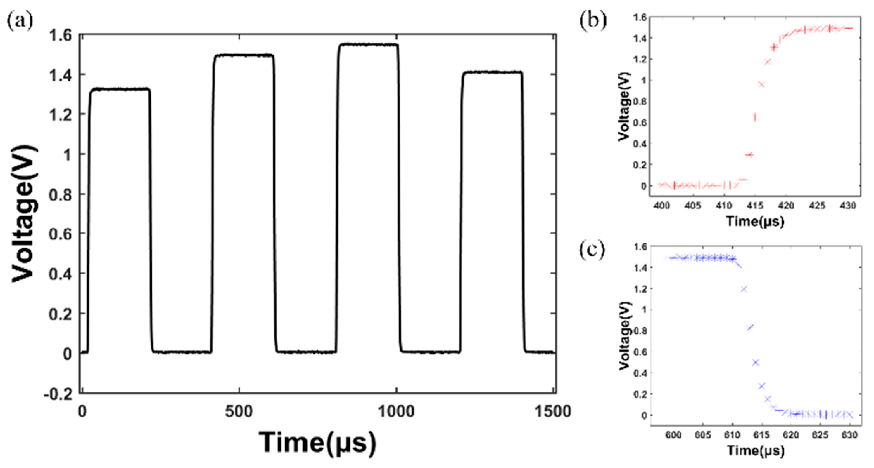
The test flow of running time sequence is as follows: First, the control board controls DDS module to generate RF signal, which is added to AOM through RF switch on PA board and then generates TTL logic signal to control RF switch. Finally, the voltage signal output by PD2 is collected by ADC on the control board, and the response time of AOM can be measured. The timing test is shown in Figure 11. The laser light power passing through the AOM can be changed by DDS, and the clock laser can be turned on and off. The response time of the AOM is less than 6 μs, which meets the requirements of timing control of the 40Ca+ optical clock.
4. Conclusions
We have developed a miniaturized multi-channel RF module, that can provide signal source and power amplifier at the same time with a 170 mm ×230 mm ×80 mm size. By the PLL+DDS, two-stage power amplification technique and choosing different kinds of filters for appropriate frequency, the output of this module within 400 MHz can reach a very low phase noise with a resolution of 4 μHz, and the output power of this module is up to +33 dBm (2 W) 100 MHz. Compared to the commercial module, the phase noise is reduced by more than 25 dBc /Hz@1Hz, and the third harmonic suppression ratio at the frequency point of 300 MHz is reduced by more than 20 dBm. with a volume only 20% of the commercial module. Then this module was successfully used to stability the 729 nm laser power in a 40Ca+ optical clock, the standard deviation of the optical power fluctuation can be decreased by 5 times with a turned on and off response time within 6 μs. The timing control experiment results of this module show that this module can satisfy the RF requirements of the 40Ca+ optical clock system, is of great significance for the transportable 40Ca+ optical clock. Nevertheless, this module can also be extended to other quantum systems such as quantum absolute gravimeter, quantum gyro and quantum computer.
Author Contributions
Conceptualization, B.W. and H.G.; software, Y.H.Y.; validation, R.M.H., H.Q.Z. and B.W.; formal analysis, Y.H., K.L.G. and H.C.M.; writing—original draft preparation, B.W.; writing—review and editing, B.W., H.Q.Z., Y.H. and H.G. All authors have read and agreed to the published version of the manuscript.
Funding
This research was funded by the National Key R&D Program of China (Grant Nos. 2022YFB3904001, 2022YFB3904004), the National Natural Science Foundation of China (Grant Nos. 12204494, 12121004, 12320101003 and 11934014), the CAS Youth Innovation Promotion Association (Grant No Y2022099), the Natural Science Foundation of Hubei Province (Grant Nos. 2022CFA013 and 2023EHA006), the CAS Project for Young Scientists in Basic Research (Grant Nos. YSBR-055 and YSBR-085), and the Interdisciplinary Cultivation Project of the Innovation Academy for Precision Measurement of Science and Technology (Grant No. S21S2201).
Institutional Review Board Statement
Not applicable.
Informed Consent Statement
Not applicable.
Data Availability Statement
Relevant data are available upon reasonable request to the corresponding author.
Conflicts of Interest
The authors declare no conflicts of interest.
References
- Monroe, C.; Meekhof, D.M.; King, B.E.; Jefferts, S.R.; Itano, W.M.; Wineland, D.J.; Gould, P. Resolved-sideband Raman cooling of a bound atom to the 3D zero-point energy. Phys Rev Lett 1995, 75, 4011–4014. [Google Scholar] [CrossRef]
- Li, J.J.; Zhang, F.F.; Wang, Z.M.; Xu, Y.C.; Liu, X.C.; Zong, N.; Zhang, S.J.; Xu, F.L.; Yang, F.; Yuan, L.; et al. High-energy single-frequency 167 nm deep-ultraviolet laser. Opt Lett 2018, 43, 2563–2566. [Google Scholar] [CrossRef] [PubMed]
- Chang, S.; Kwon, T.Y.; Lee, H.S.; Minogin, V.G. Laser sub-Doppler cooling of atoms in an arbitrarily directed magnetic field. Physical Review A 2002, 66, 043404. [Google Scholar] [CrossRef]
- Larson, D.J.; Bergquist, J.C.; Bollinger, J.J.; Itano, W.M.; Wineland, D.J. Sympathetic cooling of trapped ions: A laser-cooled two-species nonneutral ion plasma. Phys Rev Lett 1986, 57, 70–73. [Google Scholar] [CrossRef] [PubMed]
- Wells, A.L.; Cook, R.J. Simple theory of sideband cooling. Phys Rev A 1990, 41, 3916–3923. [Google Scholar] [CrossRef] [PubMed]
- Taichenachev, A.V.; Tumaikin, A.M.; Yudin, V.I.; Hollberg, L. Two-dimensional sideband Raman cooling and Zeeman-state preparation in an optical lattice. Physical Review A 2001, 63, 033402. [Google Scholar] [CrossRef]
- Sun, Y.; Yao, Y.; Hao, Y.; Yu, H.; Jiang, Y.; Ma, L. Laser stabilizing to ytterbium clock transition with Rabi and Ramsey spectroscopy. Chinese Optics Letters 2020, 18, 070201. [Google Scholar] [CrossRef]
- Xu, M.; Wu, H.; Liang, Y.; Luo, D.; Wang, P.; Tan, Y.; Shao, C. Weak-Light Phase-Locking Time Delay Interferometry with Optical Frequency Combs. Sensors (Basel) 2022, 22. [Google Scholar] [CrossRef] [PubMed]
- Bernard, J.E.; Marmet, L.; Madej, A.A. A laser frequency lock referenced to a single trapped ion. Optics Communications 1998, 150, 170–174. [Google Scholar] [CrossRef]
- Kessler, T.; Hagemann, C.; Grebing, C.; Legero, T.; Sterr, U.; Riehle, F.; Martin, M.J.; Chen, L.; Ye, J. A sub-40 mHz linewidth laser based on a silicon single-crystal optical cavity. Nature Photonics 2011, 6, 687–692. [Google Scholar] [CrossRef]
- Blumroder, U.; Kochert, P.; Frohlich, T.; Kissinger, T.; Ortlepp, I.; Flugge, J.; Bosse, H.; Manske, E. A GPS-Referenced Wavelength Standard for High-Precision Displacement Interferometry at lambda = 633 nm. Sensors (Basel) 2023, 23. [Google Scholar] [CrossRef] [PubMed]
- Takamoto, M.; Ushijima, I.; Ohmae, N.; Yahagi, T.; Kokado, K.; Shinkai, H.; Katori, H. Test of general relativity by a pair of transportable optical lattice clocks. Nature photonics 2020, 14, 411–415. [Google Scholar] [CrossRef]
- Sanner, C.; Huntemann, N.; Lange, R.; Tamm, C.; Peik, E.; Safronova, M.S.; Porsev, S.G. Optical clock comparison for Lorentz symmetry testing. Nature 2019, 567, 204–208. [Google Scholar] [CrossRef] [PubMed]
- Liu, D.; Wu, L.; Xiong, C.; Bao, L. Geopotential Difference Measurement Using Two Transportable Optical Clocks’ Frequency Comparisons. Remote Sensing 2024, 16. [Google Scholar] [CrossRef]
- Lisdat, C.; Grosche, G.; Quintin, N.; Shi, C.; Raupach, S.M.; Grebing, C.; Nicolodi, D.; Stefani, F.; Al-Masoudi, A.; Dorscher, S.; et al. A clock network for geodesy and fundamental science. Nat Commun 2016, 7, 12443. [Google Scholar] [CrossRef] [PubMed]
- Grotti, J.; Koller, S.; Vogt, S.; Häfner, S.; Sterr, U.; Lisdat, C.; Denker, H.; Voigt, C.; Timmen, L.; Rolland, A.; et al. Geodesy and metrology with a transportable optical clock. Nature physics 2018, 14, 437–441. [Google Scholar] [CrossRef]
- Boldbaatar, E.; Grant, D.; Choy, S.; Zaminpardaz, S.; Holden, L. Evaluating Optical Clock Performance for GNSS Positioning. Sensors (Basel) 2023, 23. [Google Scholar] [CrossRef]
- Safronova, M.S.; Porsev, S.G.; Sanner, C.; Ye, J. Two Clock Transitions in Neutral Yb for the Highest Sensitivity to Variations of the Fine-Structure Constant. Phys Rev Lett 2018, 120, 173001. [Google Scholar] [CrossRef] [PubMed]
- Lemke, N.D.; Martin, K.W.; Beard, R.; Stuhl, B.K.; Metcalf, A.J.; Elgin, J.D. Measurement of Optical Rubidium Clock Frequency Spanning 65 Days. Sensors (Basel) 2022, 22. [Google Scholar] [CrossRef] [PubMed]
- Riehle, F.; Gill, P.; Arias, F.; Robertsson, L. The CIPM list of recommended frequency standard values: guidelines and procedures. Metrologia 2018, 55, 188–200. [Google Scholar] [CrossRef]
- Takumi, K.; Akifumi, T.; Daisuke, A.; Akio, K.; Akiko, N.; Kazumoto, H.; Yusuke, H.; Masato, W.; Hajime, I.; Takehiko, T.; et al. Search for Ultralight Dark Matter from Long-Term Frequency Comparisons of Optical and Microwave Atomic Clocks. Physical review letters 2022, 129, 241301–241301. [Google Scholar]
- Huang, Y.; Guan, H.; Liu, P.; Bian, W.; Ma, L.; Liang, K.; Li, T.; Gao, K. Frequency Comparison of Two (40)Ca(+) Optical Clocks with an Uncertainty at the 10(-17) Level. Phys Rev Lett 2016, 116, 013001. [Google Scholar] [CrossRef] [PubMed]
- Cao, J.; Zhang, P.; Shang, J.; Cui, K.; Yuan, J.; Chao, S.; Wang, S.; Shu, H.; Huang, X. A compact, transportable single-ion optical clock with 7.8 × 10⁻¹⁷ systematic uncertainty. Applied Physics B 2017, 123. [Google Scholar] [CrossRef]
- Hao, Y.; Hu, R.; Zhang, B.; Zeng, M.; Zhang, H.; Ma, Z.; Huang, Y.; Chen, Q.; Gao, K.; Guan, H. Stability improvement of (40)Ca(+) optical clock by using a transportable ultra-stable cavity. Opt Express 2024, 32, 4081–4092. [Google Scholar] [CrossRef]
- Zhang, B.; Huang, Y.; Zhang, H.; Hao, Y.; Zeng, M.; Guan, H.; Gao, K. Progress on the 40Ca+ ion optical clock*. Chinese Physics B 2020, 29, 74209–074209. [Google Scholar] [CrossRef]
- Ming-Dong, Z.; Lin, Y.; Xi, Q.; Wen-Zhe, Z.; Yiheng, L.; Du, J. FPGA based hardware platform for trapped-ion-based multi-level quantum systems. Chinese Physics B 2023, 32. [Google Scholar]
- Shaik Peerla, R.; Dutta, A.; Sahoo, B.D. An Extended Range Divider Technique for Multi-Band PLL. Journal of Low Power Electronics and Applications 2023, 13. [Google Scholar] [CrossRef]
- Song, Y.J.; Pany, T.; Won, J.H. Theoretical Upper and Lower Limits for Normalized Bandwidth of Digital Phase-Locked Loop in GNSS Receivers. Sensors (Basel) 2023, 23. [Google Scholar] [CrossRef]
- Blatnik, A.; Batagelj, B. Wideband Low Phase-Noise Signal Generation Using Coaxial Resonator in Cascaded Phase Locked Loop. Electronics 2024, 13. [Google Scholar] [CrossRef]
- Farhad, B.; Alireza, G.R.; Samad, S.; Massoud, T. A fast settling frequency synthesizer with switched-bandwidth loop filter. International Journal of Circuit Theory and Applications 2021, 49, 2021–2031. [Google Scholar]
- Sun, L.; Luo, Y.; Deng, Z.; Wang, J.; Liu, B. Novel Power-Efficient Fast-Locking Phase-Locked Loop Based on Adaptive Time-to-Digital Converter-Aided Acceleration Compensation Technology. Electronics 2024, 13. [Google Scholar] [CrossRef]
- Zhang, B.; Huang, Y.; Hao, Y.; Zhang, H.; Zeng, M.; Guan, H.; Gao, K. Improvement in the stability of a 40Ca+ ion optical clock using the Ramsey method. Journal of Applied Physics 2020, 128. [Google Scholar] [CrossRef]
Figure 1.
Phase Noise Simulation Diagram of PLL. The phase noise in the loop bandwidth is determined by the reference signal source, and the phase noise outside the loop bandwidth is determined by the VCO.
Figure 1.
Phase Noise Simulation Diagram of PLL. The phase noise in the loop bandwidth is determined by the reference signal source, and the phase noise outside the loop bandwidth is determined by the VCO.
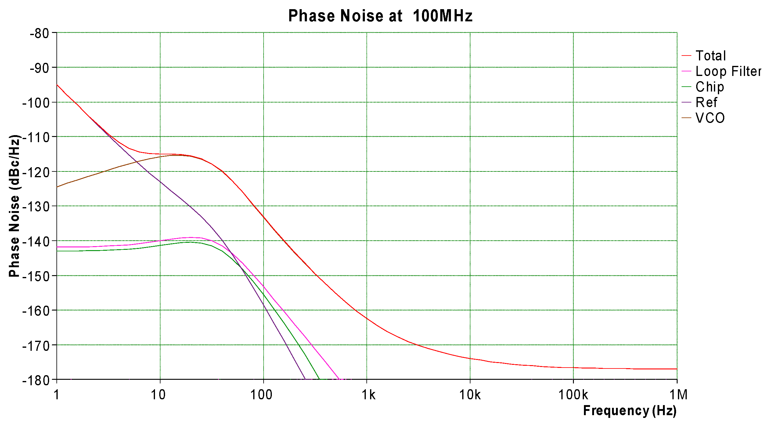
Figure 2.
System block diagram of integrated RF Source. The abbreviations in the figure mean as follows: OCXO: oven-controlled crystal oscillator; SW: signal selector switch; PFD: phase-frequency detector; LF: loop filter; VCO: Voltage Controlled Oscillator; PS: power splitter.
Figure 2.
System block diagram of integrated RF Source. The abbreviations in the figure mean as follows: OCXO: oven-controlled crystal oscillator; SW: signal selector switch; PFD: phase-frequency detector; LF: loop filter; VCO: Voltage Controlled Oscillator; PS: power splitter.
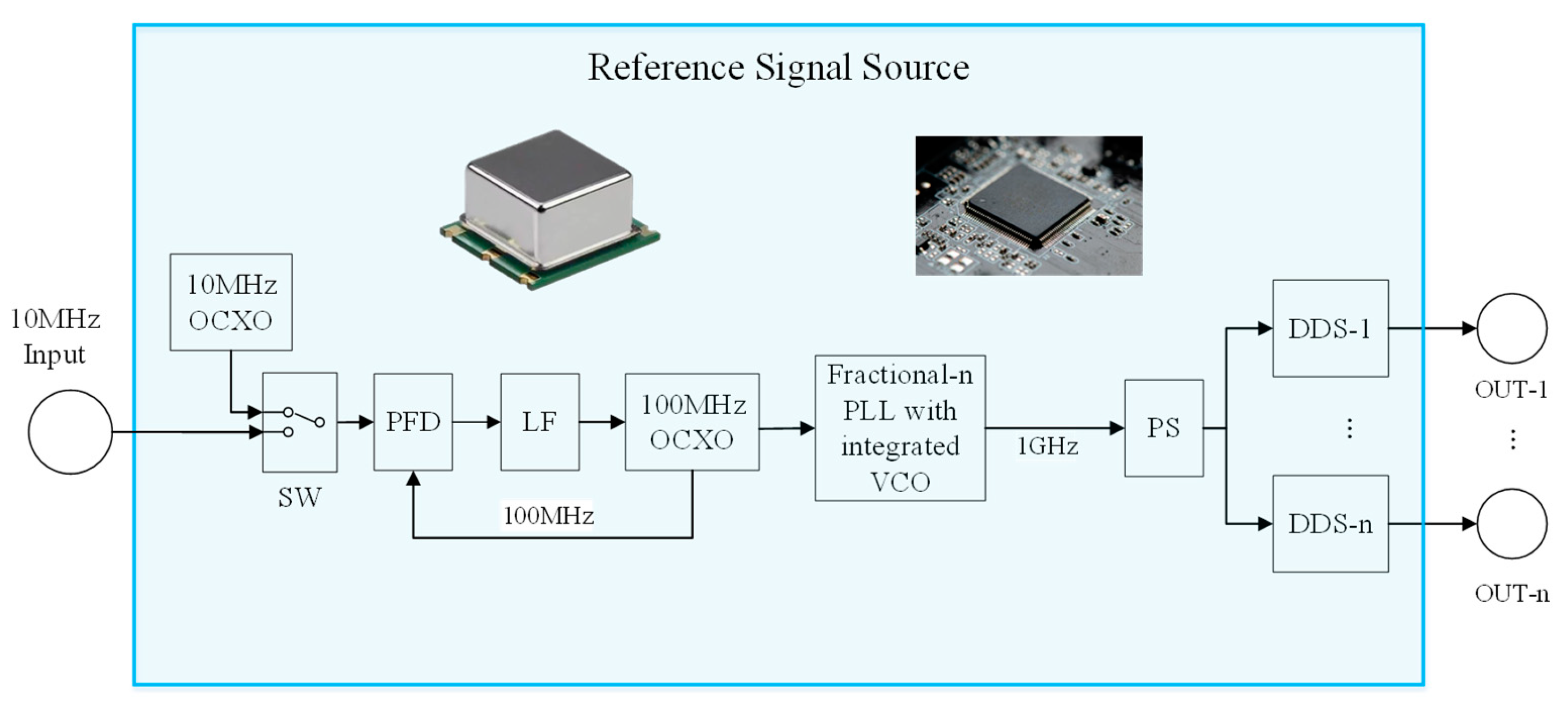
Figure 3.
Schematic diagram of power amplifier Circuit. The abbreviations in the figure mean as follows: VCA: voltage control attenuator; LNA: low-noise amplifier; LPF: low-pass filter; PA: power amplifier; PD: power detector.
Figure 3.
Schematic diagram of power amplifier Circuit. The abbreviations in the figure mean as follows: VCA: voltage control attenuator; LNA: low-noise amplifier; LPF: low-pass filter; PA: power amplifier; PD: power detector.
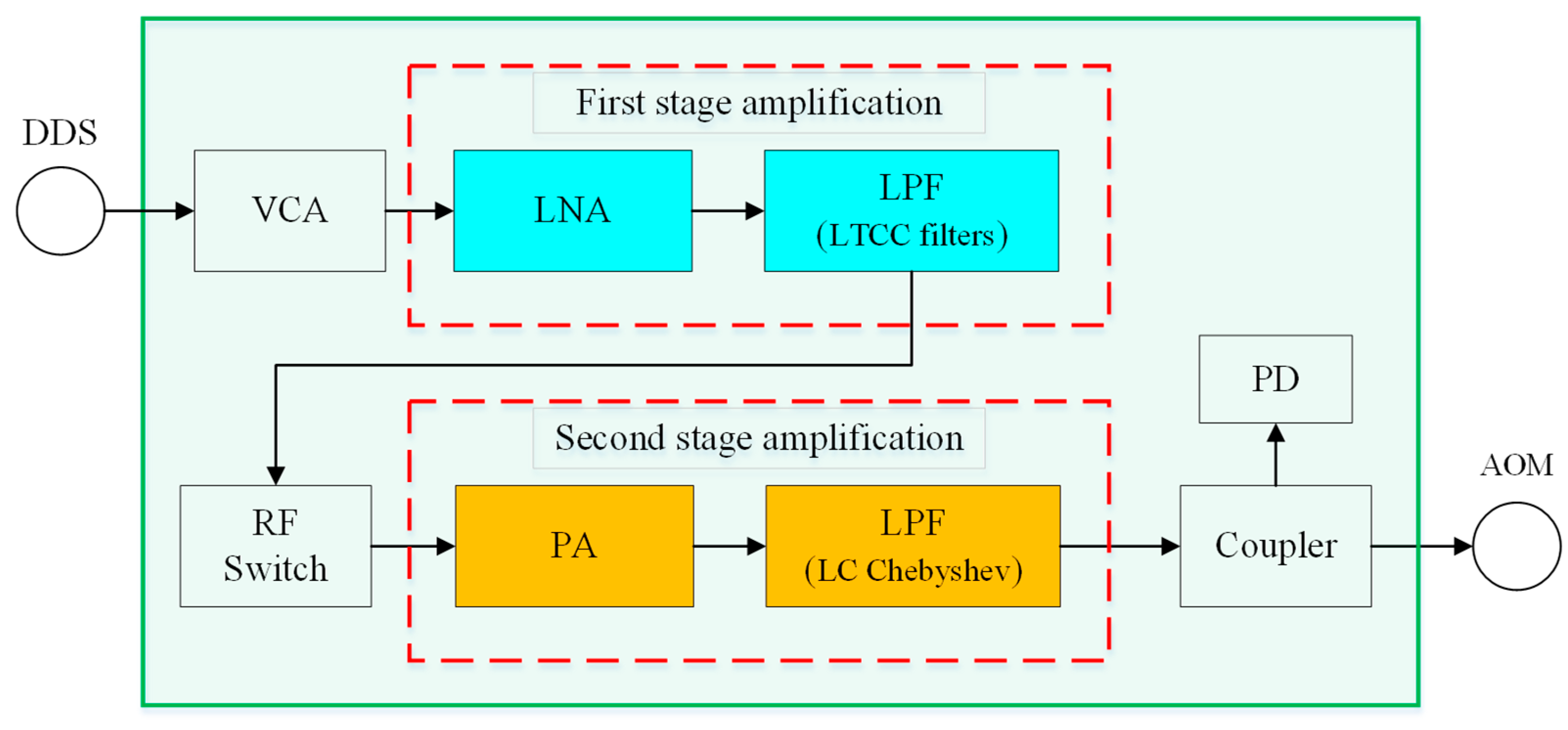
Figure 4.
Schematic Diagram of Resistive Coupler/Power Divider.
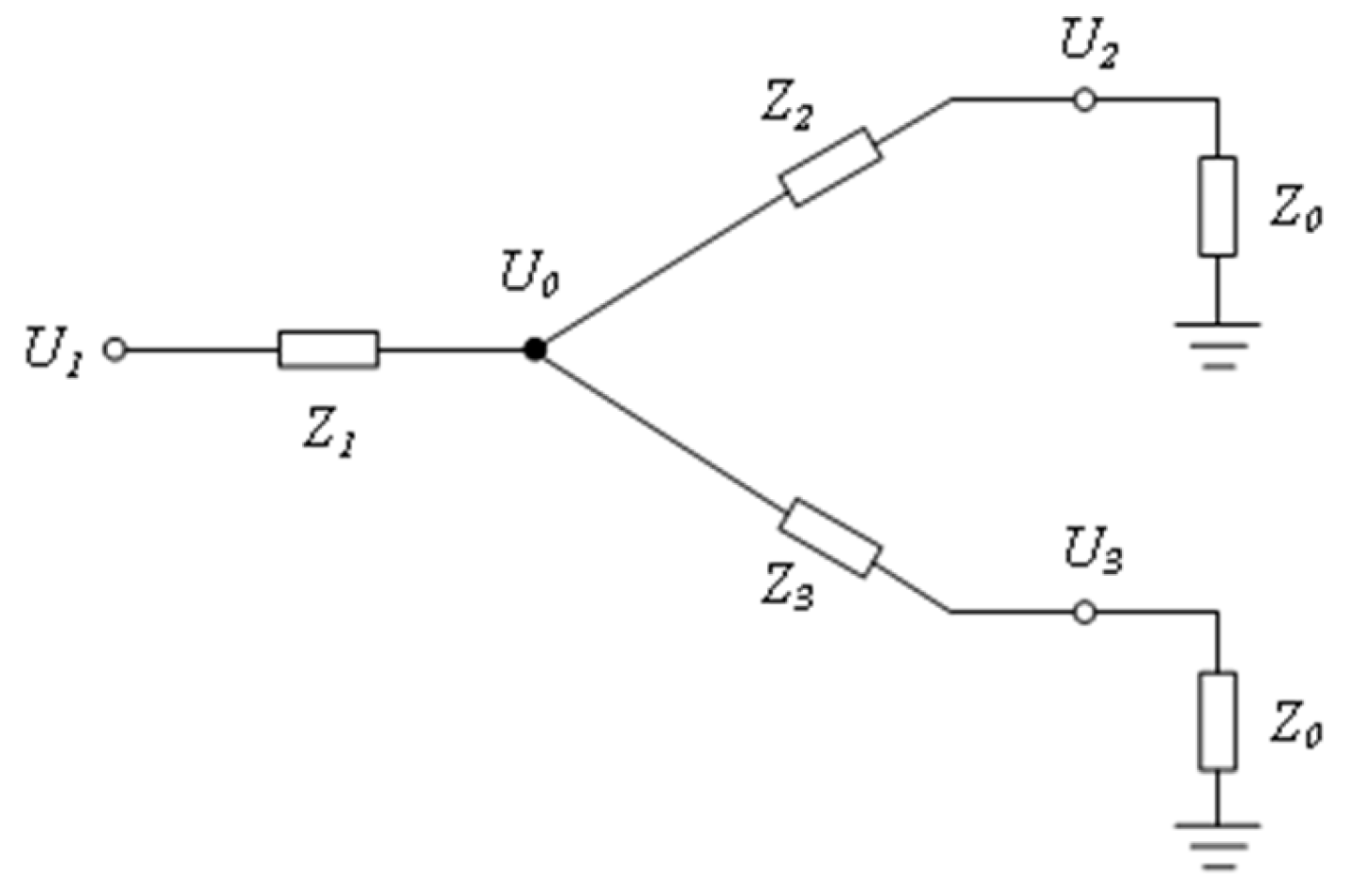
Figure 5.
Photograph of the PCB boards. (a) is 1 GHz board, (b) is DDS board, (c) is PA board.
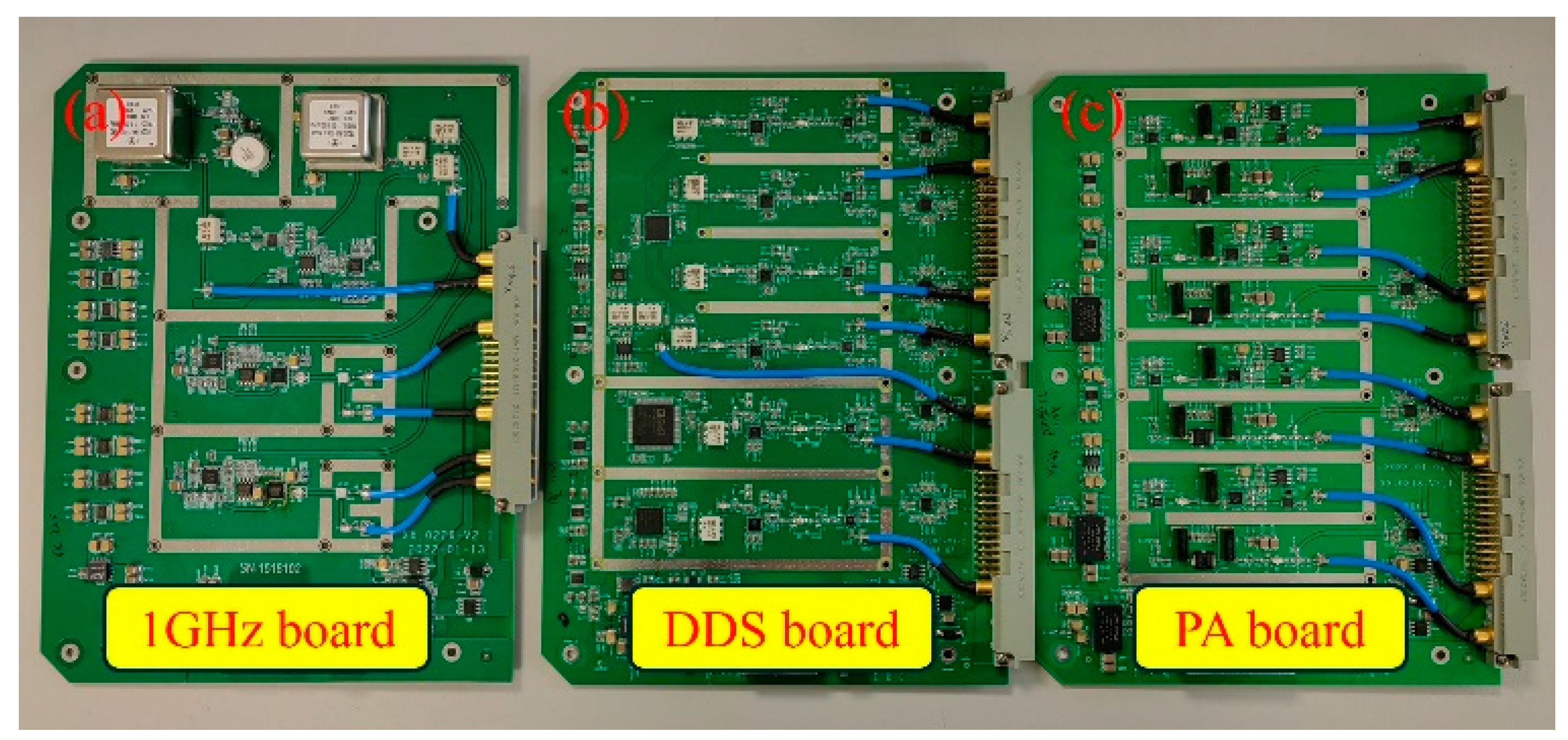
Figure 6.
Output signal phase noise test chart. The phase noise of the RF module is better than that of the commercial signal source by more than 25 dBc/Hz at the frequency point of 1 Hz.
Figure 6.
Output signal phase noise test chart. The phase noise of the RF module is better than that of the commercial signal source by more than 25 dBc/Hz at the frequency point of 1 Hz.
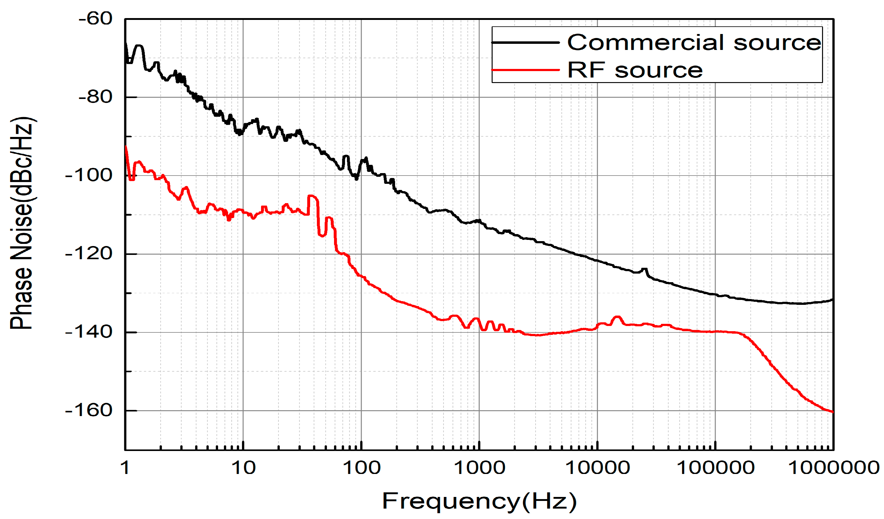
Figure 7.
Output signal spectrum test chart. (a) is PA board 100MHz carrier spectrum diagram; (b) is commercial source 100 MHz carrier spectrum diagram. The third harmonic rejection ratio of the PA board is better than commercial source by more than 20 dBm.
Figure 7.
Output signal spectrum test chart. (a) is PA board 100MHz carrier spectrum diagram; (b) is commercial source 100 MHz carrier spectrum diagram. The third harmonic rejection ratio of the PA board is better than commercial source by more than 20 dBm.
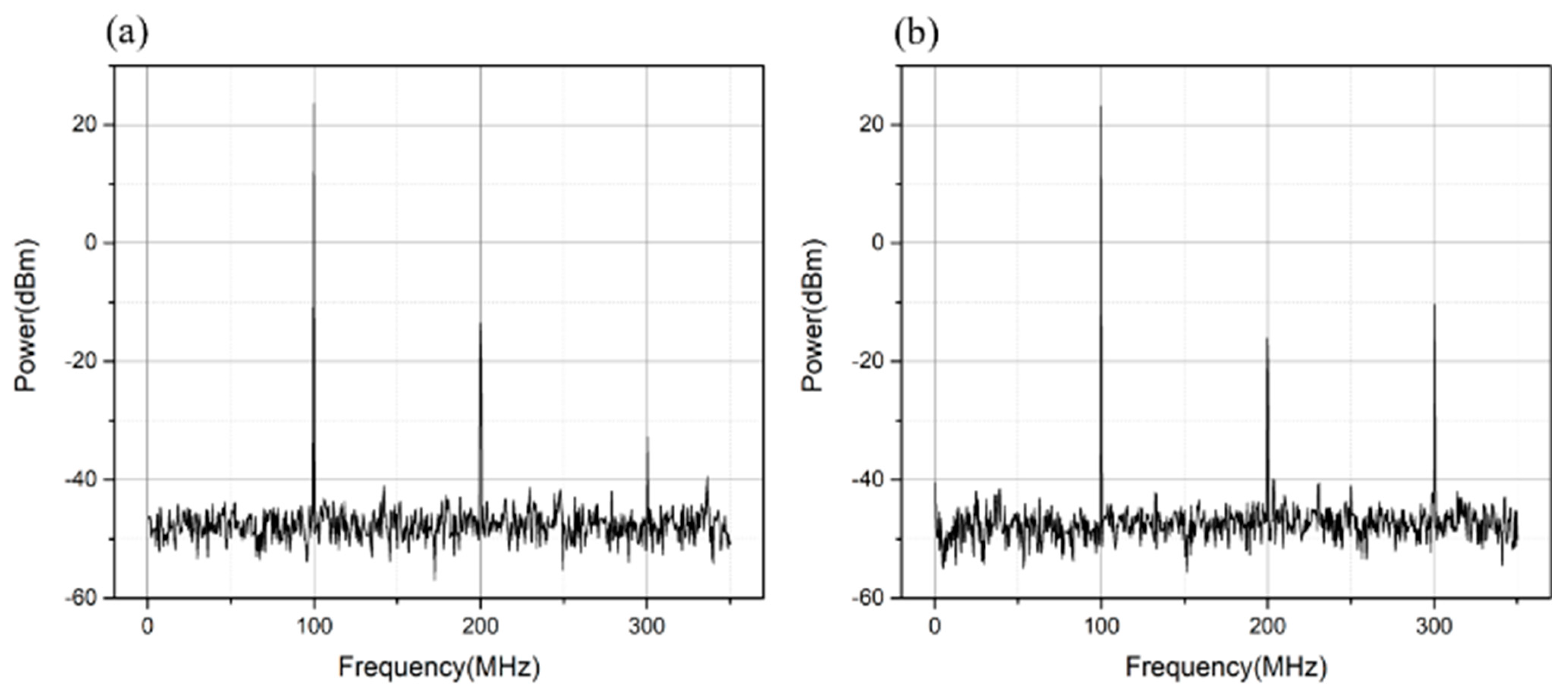
Figure 8.
Functional block diagram of the experimental device. The abbreviations in the figure mean follows: OFC: optical fiber coupler; λ/2: half-wave plate; λ/4: quarter-wave plate; PBS: polarizing beam splitter; BS: beam splitter; PD: photo detector; PID: proportional-integral-derivative circuit.
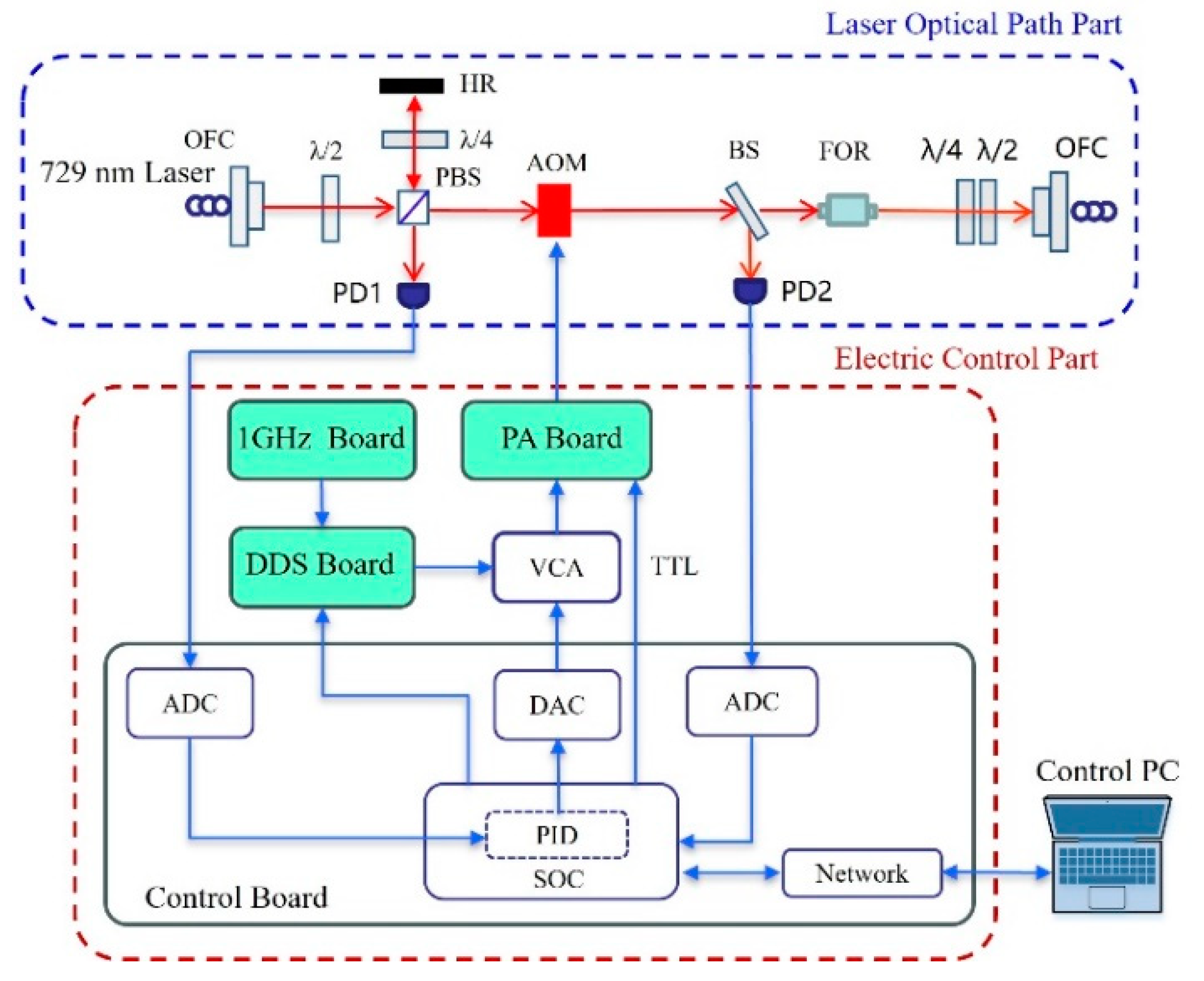
Figure 9.
Comparison chart before and after optical power stabilization. According to the optical power data converted from the sampling voltage, the standard deviation of optical power fluctuation has decreased by 5 times after the clock laser power stabilization is turned on.
Figure 9.
Comparison chart before and after optical power stabilization. According to the optical power data converted from the sampling voltage, the standard deviation of optical power fluctuation has decreased by 5 times after the clock laser power stabilization is turned on.
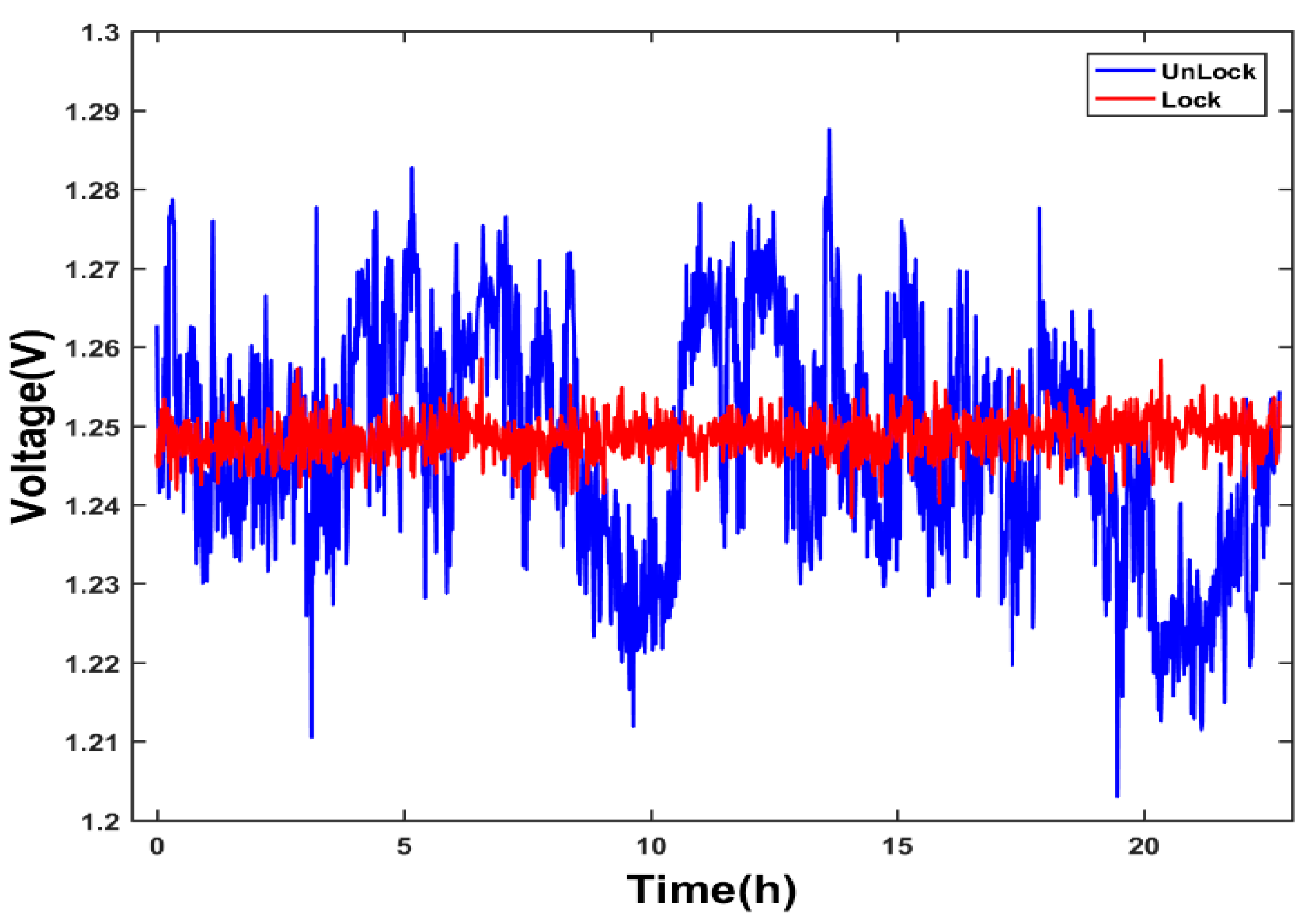
Figure 10.
Time sequence diagram of optical clock operation. Color blocks and white blocks respectively represent the opening and closing of the corresponding beams, and Delay1 and Delay2 are the waiting time for all lasers except the detection laser to close or open the mechanical shutter.
Figure 10.
Time sequence diagram of optical clock operation. Color blocks and white blocks respectively represent the opening and closing of the corresponding beams, and Delay1 and Delay2 are the waiting time for all lasers except the detection laser to close or open the mechanical shutter.
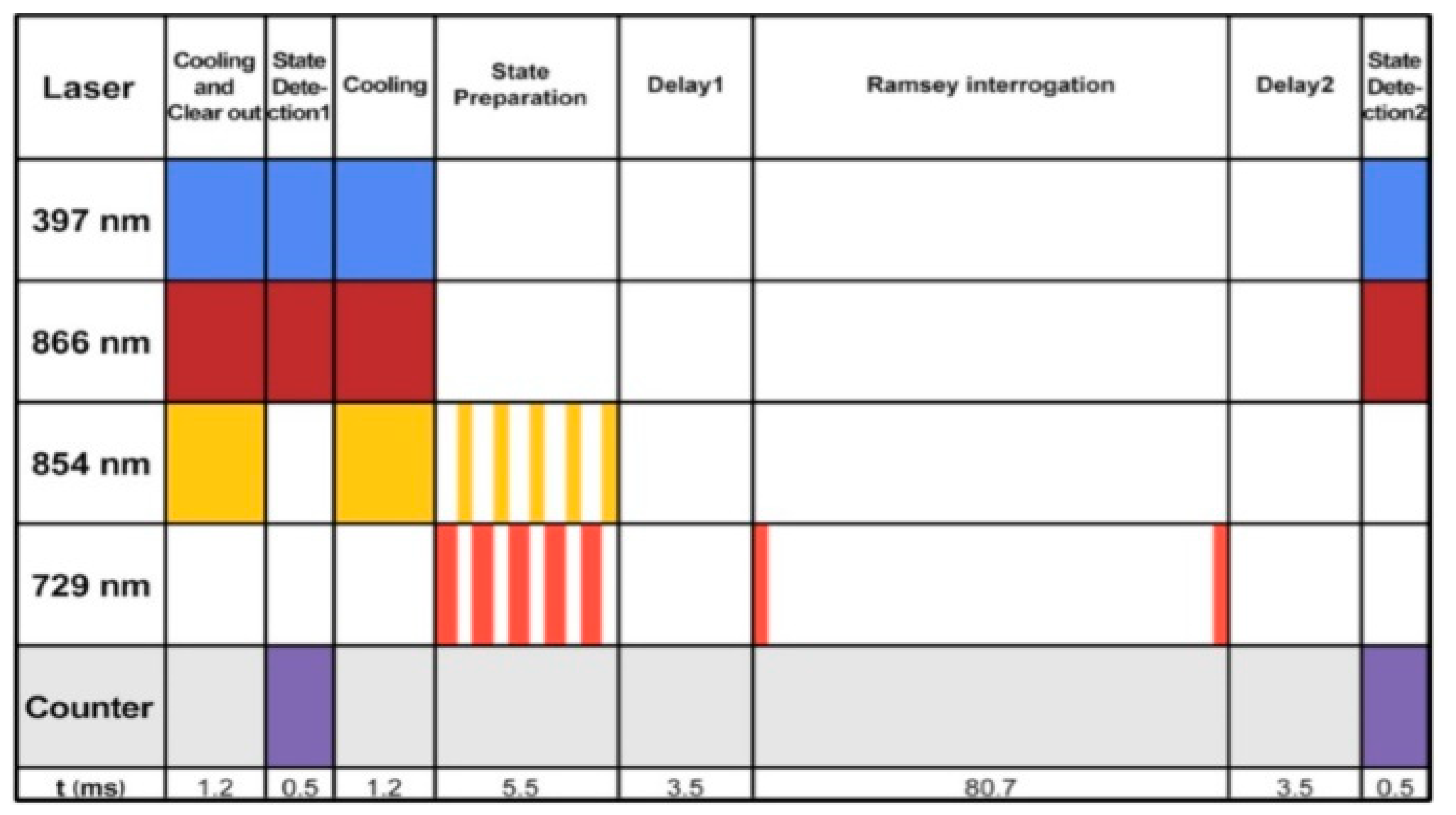
Figure 11.
Sequential operation test chart(a), enlarged diagram of rising edge(b), enlarged diagram of falling edge(c). The laser light power passing through the AOM can be changed by DDS, and the clock laser can be turned on and off. The response time of the AOM is less than 6 μs.
Figure 11.
Sequential operation test chart(a), enlarged diagram of rising edge(b), enlarged diagram of falling edge(c). The laser light power passing through the AOM can be changed by DDS, and the clock laser can be turned on and off. The response time of the AOM is less than 6 μs.
Disclaimer/Publisher’s Note: The statements, opinions and data contained in all publications are solely those of the individual author(s) and contributor(s) and not of MDPI and/or the editor(s). MDPI and/or the editor(s) disclaim responsibility for any injury to people or property resulting from any ideas, methods, instructions or products referred to in the content. |
© 2025 by the authors. Licensee MDPI, Basel, Switzerland. This article is an open access article distributed under the terms and conditions of the Creative Commons Attribution (CC BY) license (http://creativecommons.org/licenses/by/4.0/).
Copyright: This open access article is published under a Creative Commons CC BY 4.0 license, which permit the free download, distribution, and reuse, provided that the author and preprint are cited in any reuse.


