
Submitted:
13 January 2025
Posted:
14 January 2025
You are already at the latest version
Abstract
This study introduces four novel configurations of first-order and second-order multifunction inverse filters in both voltage-mode (VM) and current-mode (CM) using second-generation voltage conveyors (VCIIs). The first-order VM and CM inverse filters utilize only three passive components together with one VCII for VM and two VCIIs for CM realizations, which can provide lowpass (LP) and highpass (HP) inverse filter responses through appropriate impedance selections. The latter, second-order VM and CM multifunction inverse filters, can be constructed using the corresponding first-order inverse filters as their core circuits. These filters offer all the basic inverse filter functions, including LP, bandpass (BP), and HP inverse responses with all gains obtained from the same design. All the CM inverse filter realizations possess low-input and high-output impedances, enabling them to be fully cascaded in CM operation. For the VM filter realizations, they exhibit low-output impedances, which directly connect to the next stage without any buffer requirement. No component matching requirements are necessary for all filter responses. The non-ideal effects of the VCII on the performance of the proposed inverse filters are thoroughly examined, taking into account undesirable aspects such as tracking errors and parasitic impedances. To prove the feasibility of the designs, PSPICE program performed several simulations, utilizing model parameters of 0.18-µm CMOS technology. In addition, some testing experiments are conducted using the commercially available IC-type AD844s for evaluating the practical performance of the designed inverse filters.
Keywords:
1. Introduction
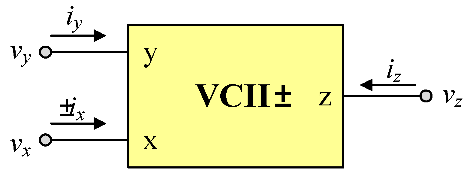
2. Second-Generation Voltage Conveyor (VCII)
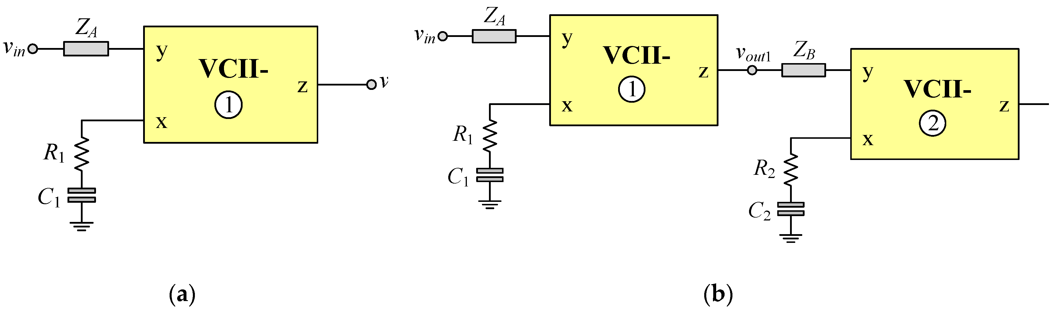
3. Proposed Cascadable Voltage-Mode Inverse Filters
3.1. First-Order VM Inverse Filter Realization
3.2. Second-Order VM Inverse Filter Realization
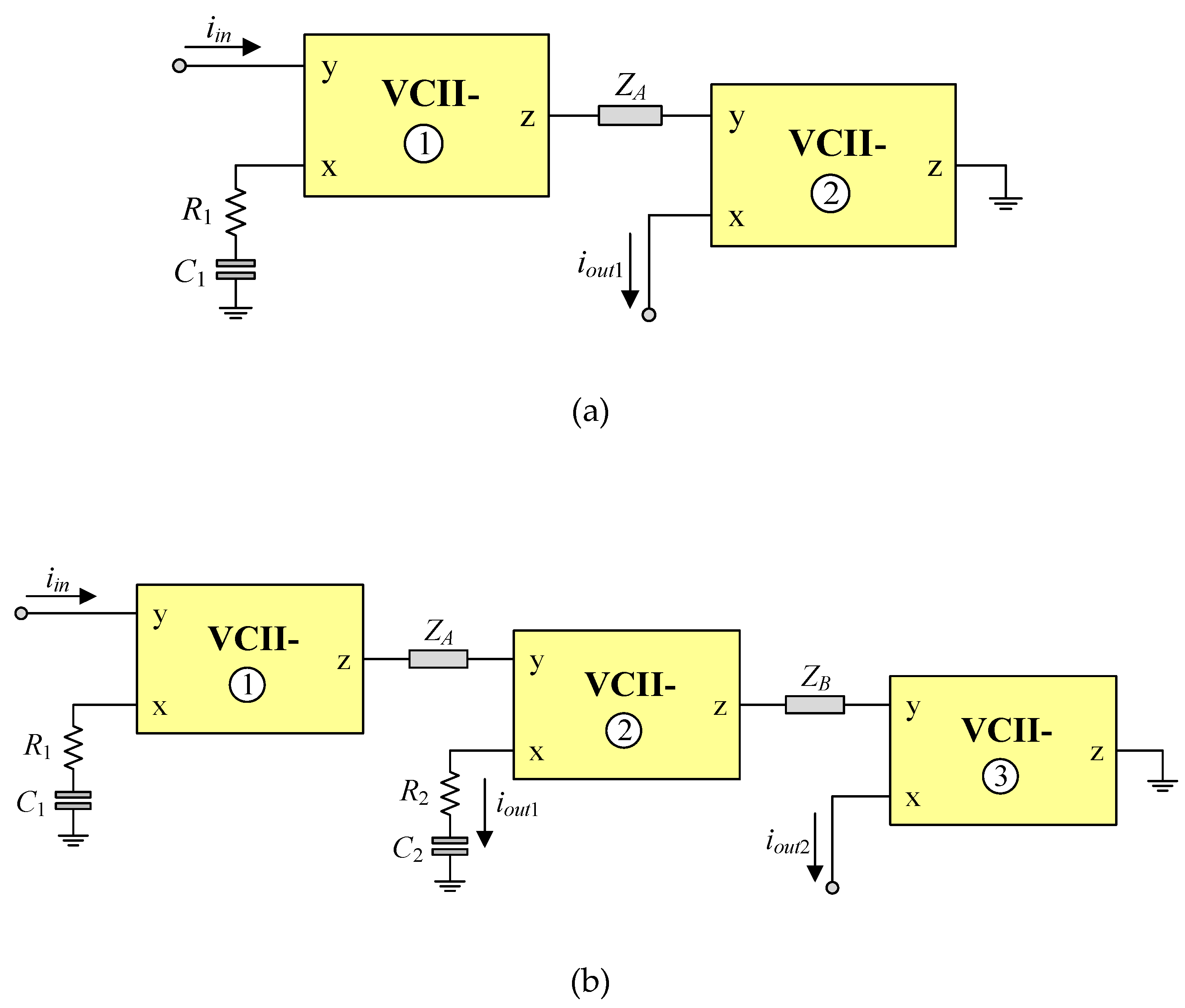
4. Proposed Cascadable Current-Mode Inverse Filters
4.1. First-Order CM Inverse Filter Realization
4.2. Second-Order CM Inverse Filter Realization
5. Tracking Error Analysis
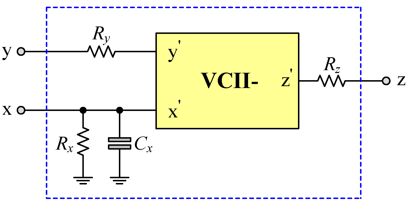
6. Parasitic Element Analysis
6.1. Parasitic Effects on VM Inverse Filter Realization
6.2. Parasitic Effects on CM Inverse Filter Realization
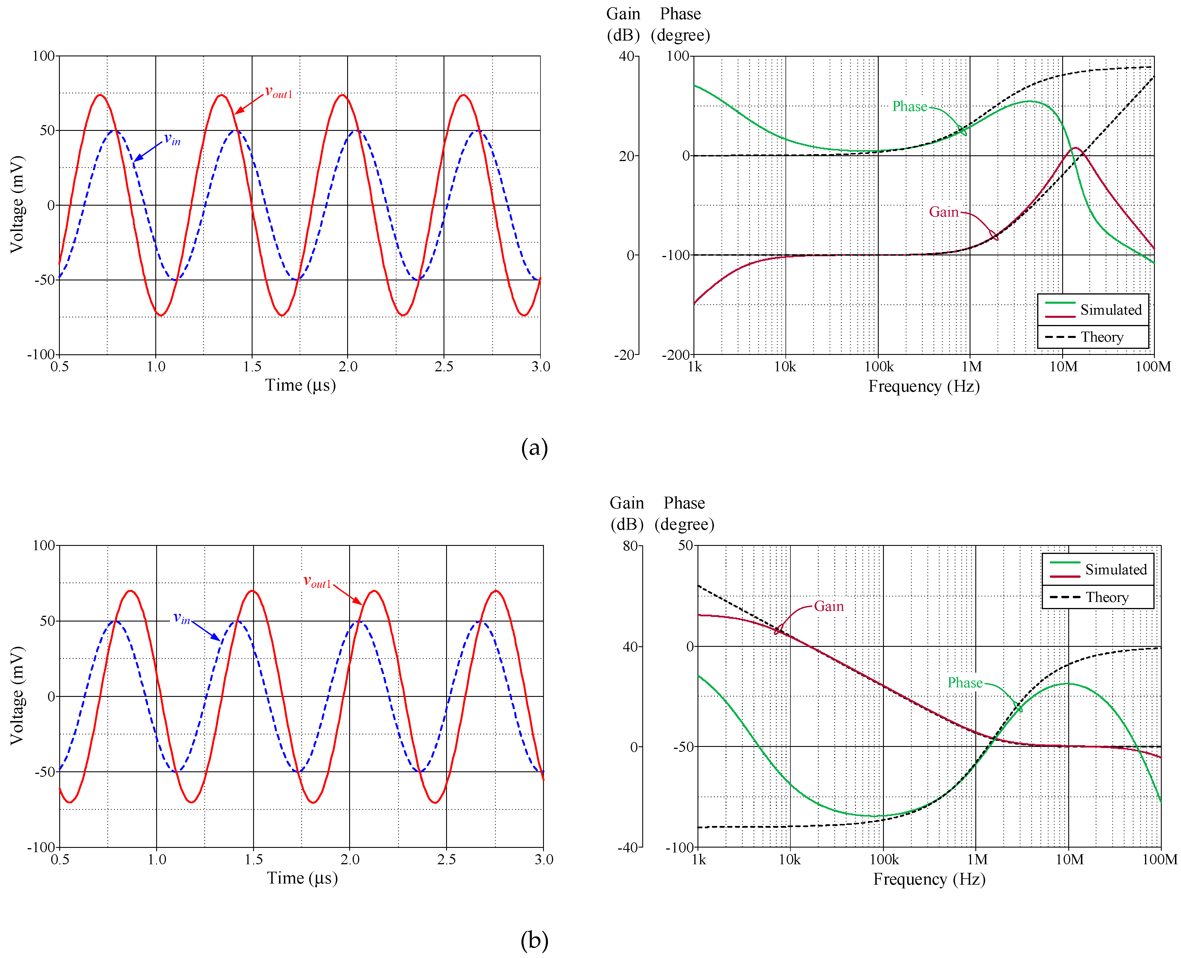
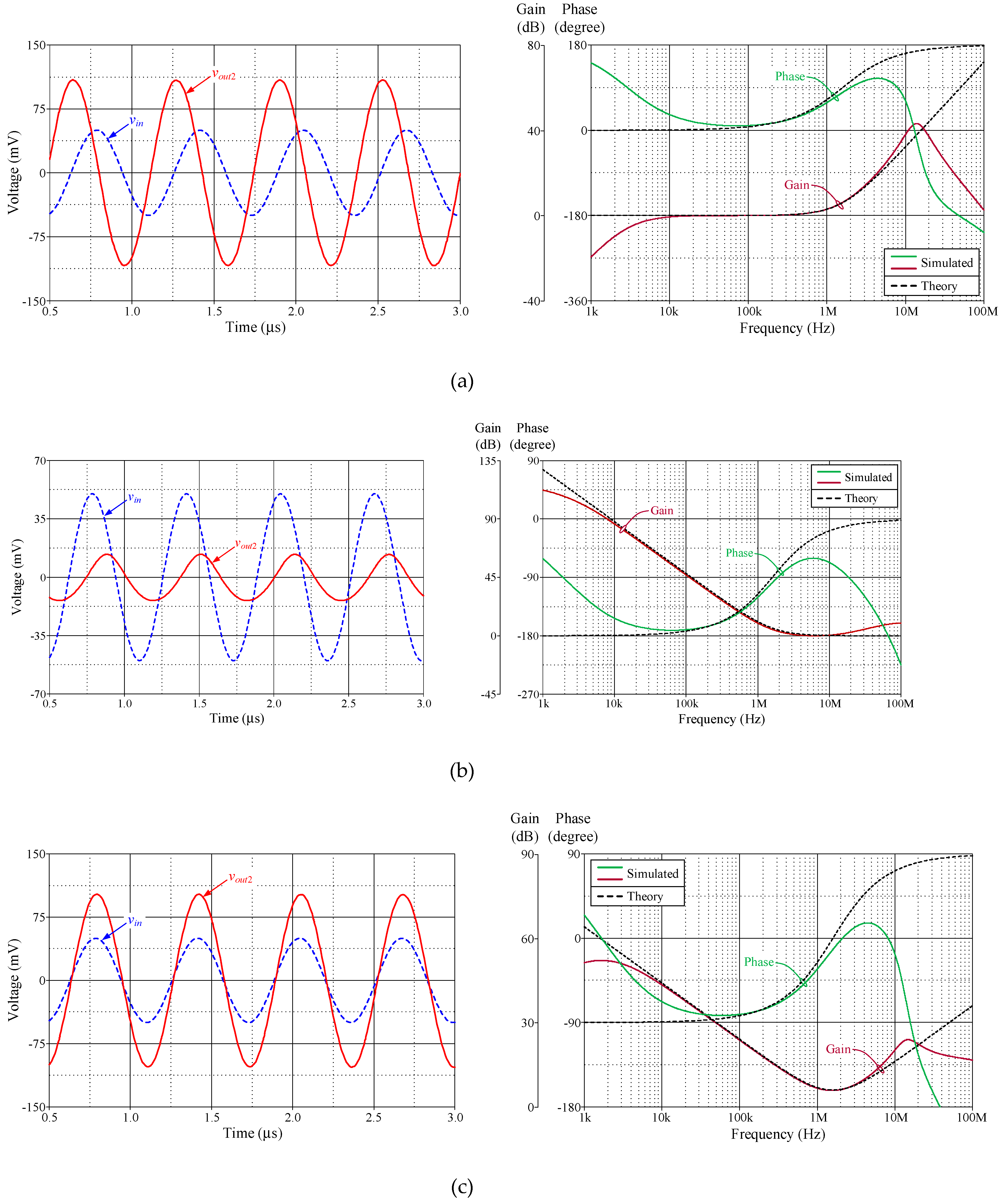
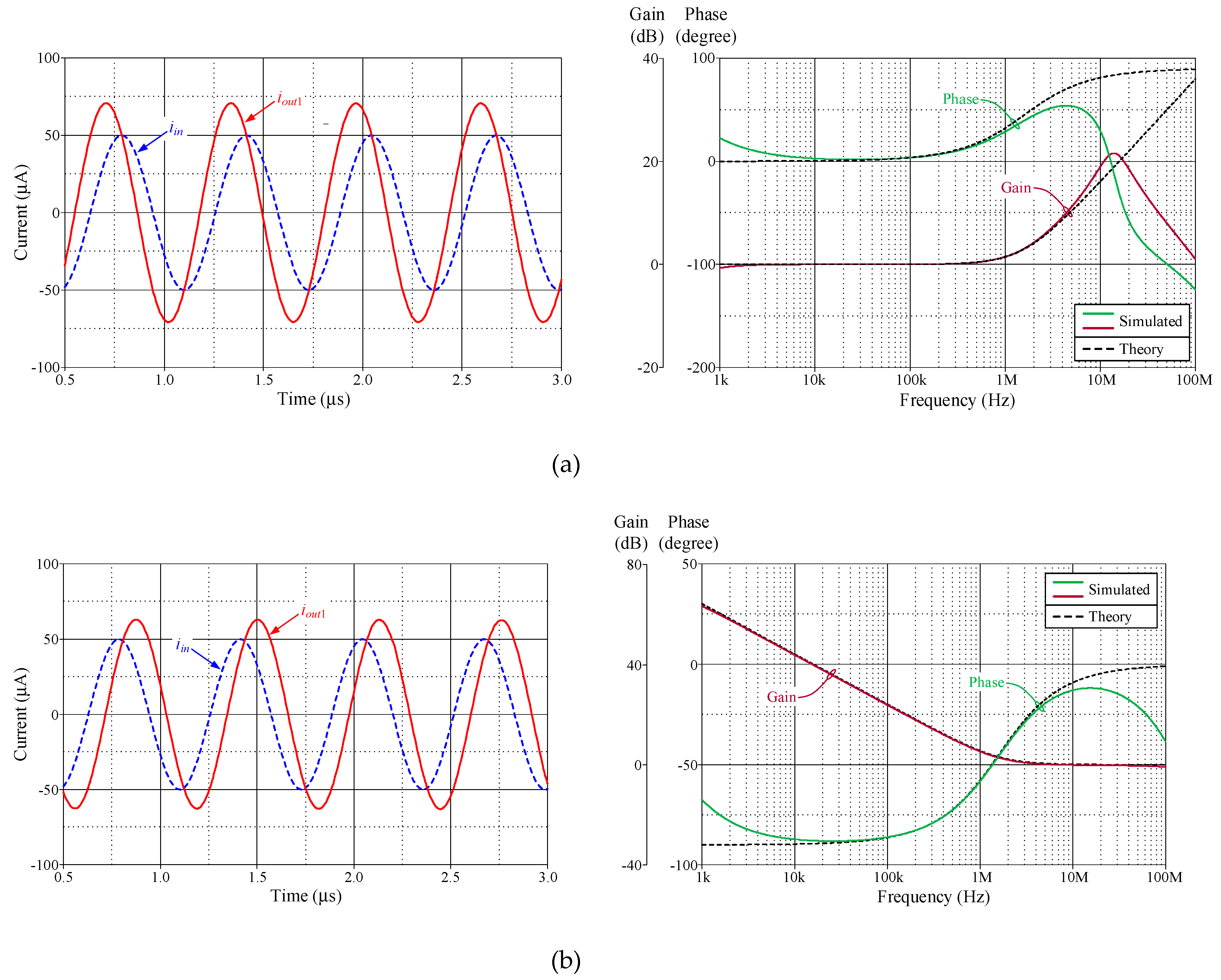
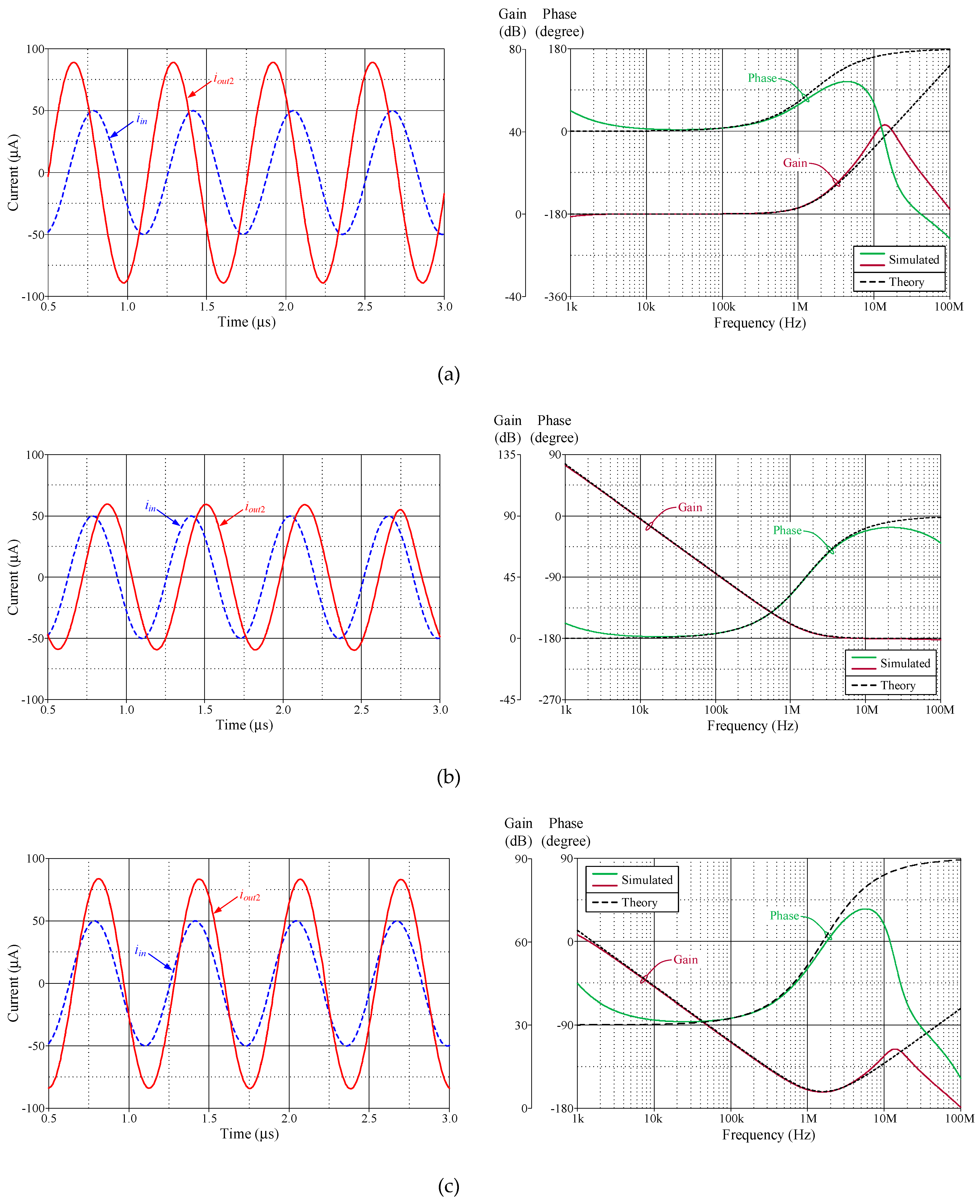
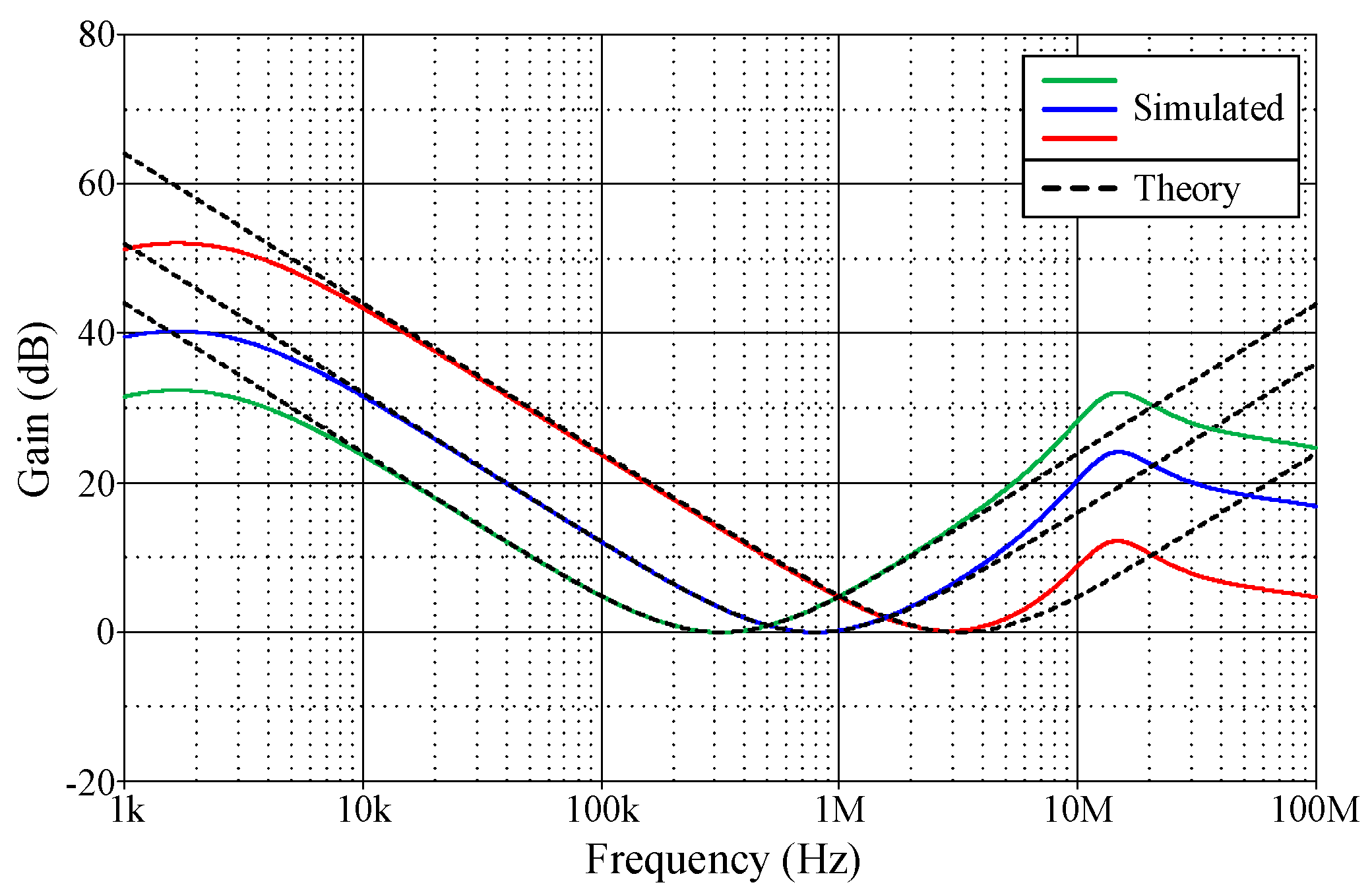
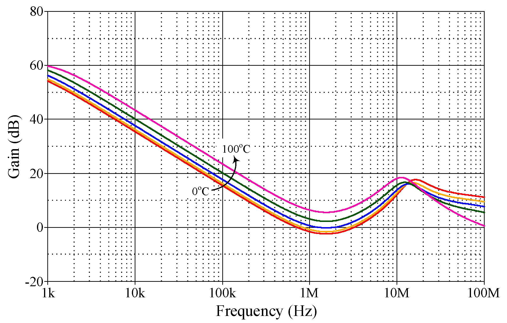
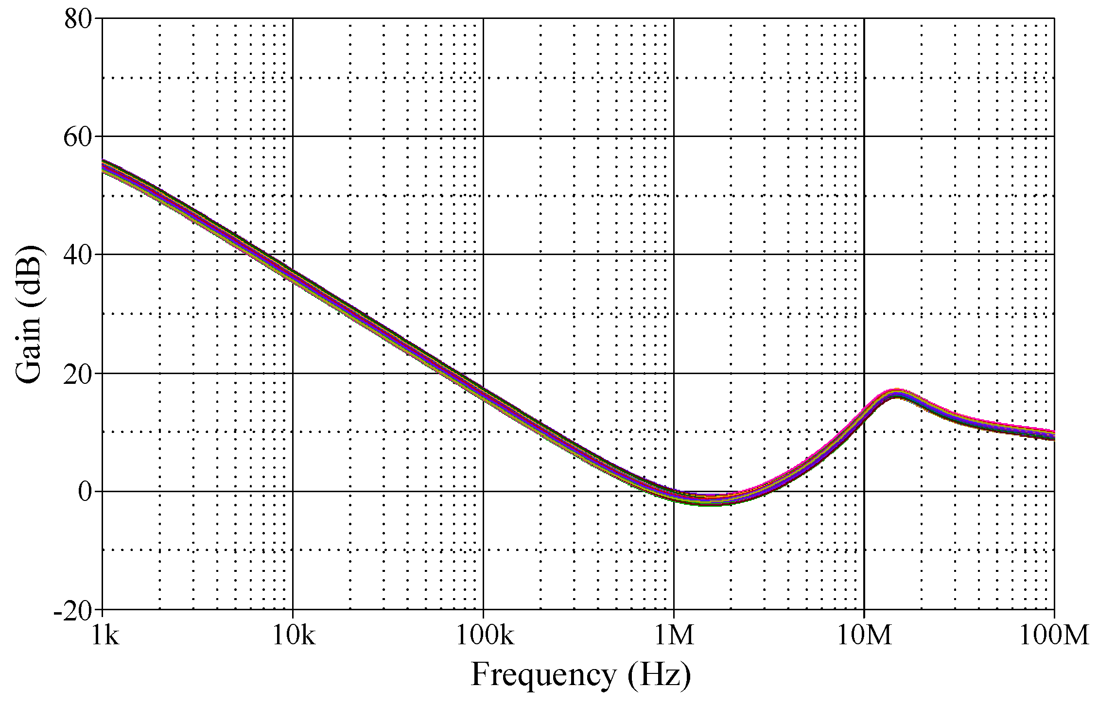
7. Simulation Verification of Filter Responses
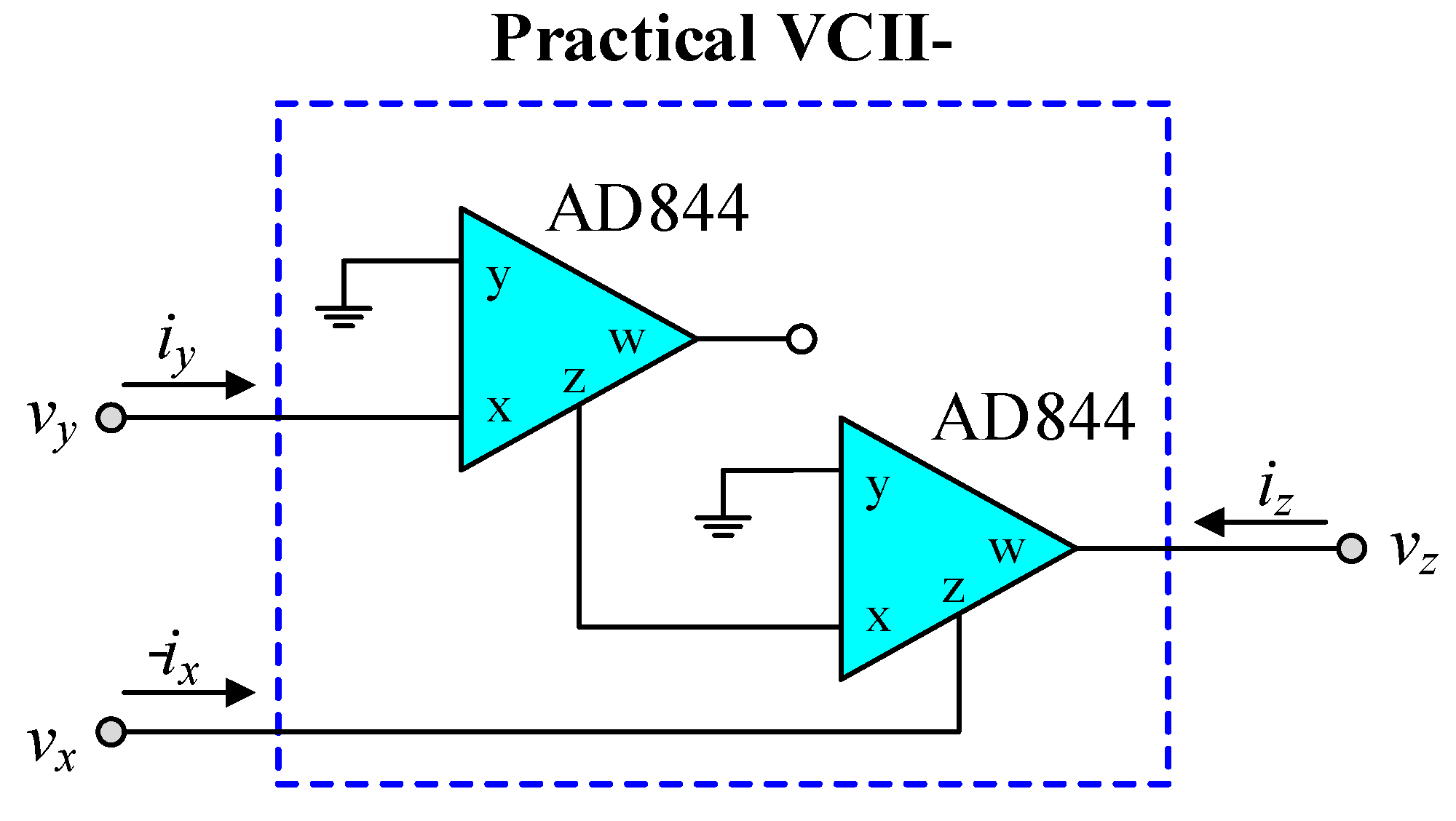
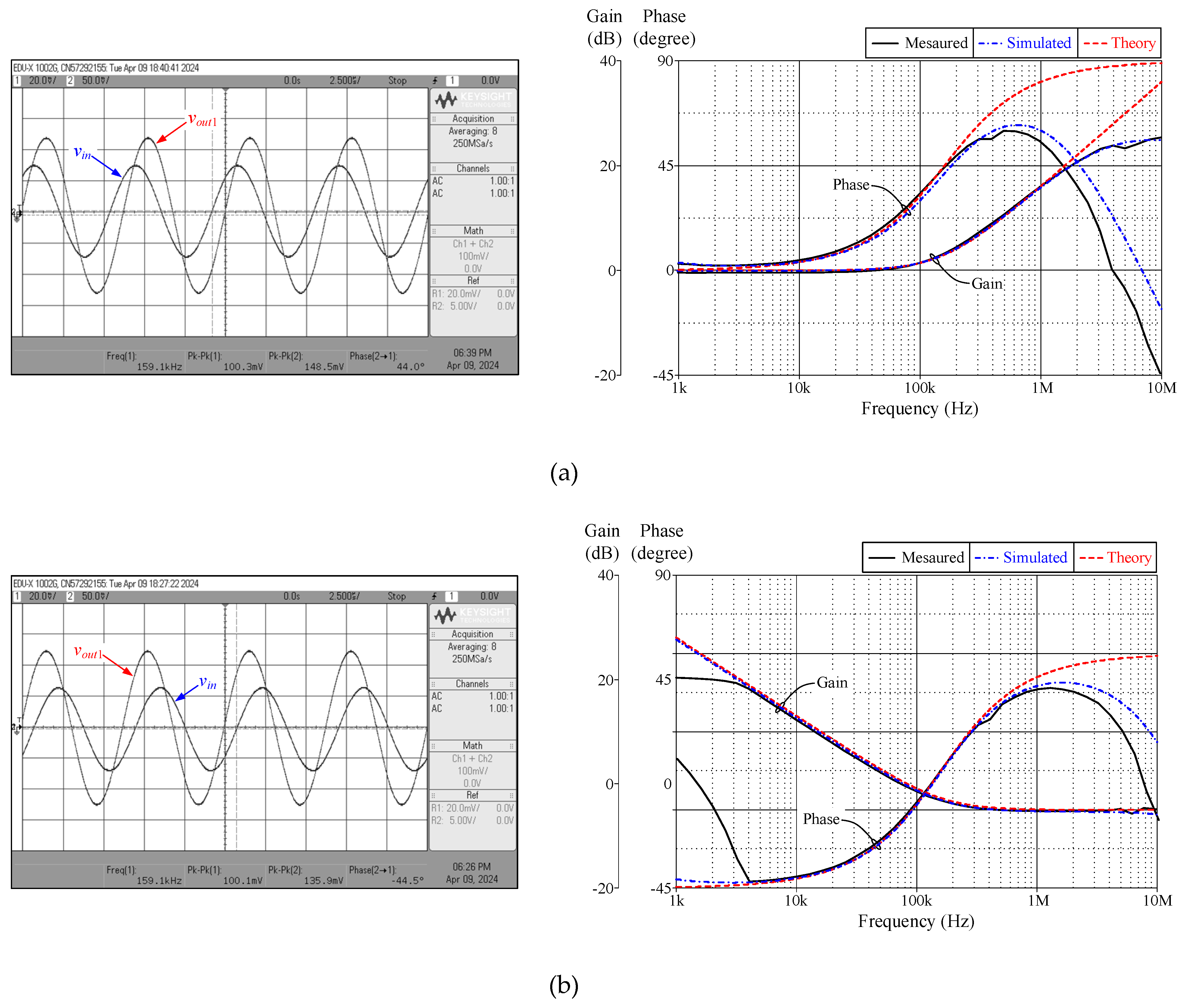
8. Experimental Verification
9. Conclusions
Author Contributions
Funding
Institutional Review Board Statement
Informed Consent Statement
Acknowledgments
Conflicts of Interest
Abbreviations
| R | Resistor |
| C | Capacitor |
| N/A | Not available |
| OA | Operational Amplifier |
| FTFN | Four Terminal Floating Nullor |
| CCII | Second-Generation Current Conveyor |
| CDTA | Current Differencing Transconductance Amplifier |
| CFOA | Current Feedback Operational Amplifier |
| MCFOA | Modified Current Feedback Operational Amplifier |
| CDBA | Current Differencing Buffered Amplifier |
| OTA | Operational Transconductance Amplifier |
| OTRA | Operational Transresistance Amplifier |
| VDTA | Voltage Differencing Transconductance Amplifier |
| VCVS | Voltage-Controlled Voltage Source |
| SW | Analog switch |
References
- Leuciuc, A. Using nullors for realisation of inverse transfer functions and characteristics. Electron. Lett. 1997, 33, 949–951. [Google Scholar] [CrossRef]
- Chipipop, B.; Surakampontorn, W. Realisation of current-mode FTFN-based inverse filter. Electron. Lett. 1999, 35, 690–692. [Google Scholar] [CrossRef]
- Wang, H. Y.; Lee, C. T. Using nullors for realisation of current-mode FTFN-based inverse filters. Electron. Lett. 1999, 35, 1889–1890. [Google Scholar] [CrossRef]
- Abuelma’atti, M. T. Identification of cascadable current-mode filters and inverse-filters using single FTFN. Frequenz 2000, 54, 1889–289. [Google Scholar]
- Shah, N. A.; Malik, M. A. FTFN-based dual inputs current-mode allpass inverse filters. Indian J. Radio Space Phys. 2005, 34, 206–209. [Google Scholar]
- Shah, N. A.; Rather, M. F. Realization of voltage-mode CCII-based allpass filter and its inverse version. Indian J. Pure Appl. Phys. 2006, 44, 269–271. [Google Scholar]
- Shah, N. A.; Quadri, M.; Iqbal, S. Z. High output impedance current-mode allpass inverse filter using CDTA. Indian J. Pure Appl. Phys. 2008, 44, 893–896. [Google Scholar]
- Gupta, S. S.; Bhaskar, D. R.; Senani, R.; Singh, A. K. ; Inverse active filters employing CFOAs. Electr. Eng. 2009, 91, 23–26. [Google Scholar] [CrossRef]
- Wang, H. Y.; Chang, S. H.; Yang, T. Y.; Tsai, P. Y. A novel multifunction CFOA-based inverse filter. Circuits Syst. 2011, 2, 14–17. [Google Scholar] [CrossRef]
- Gupta, S. S.; Bhaskar, D. R.; Senani, R. New analogue inverse filters realised with current feedback op-amps. Int. J. Electron. 2011, 98, 1103–1113. [Google Scholar] [CrossRef]
- Garg, K.; Bhagat, R.; Jaint, B. A novel multifunction modified CFOA based inverse filter. In Proc. 2012 IEEE 5th Indian Int. Conf. Power Electronics (IICPE), 6-8 Dec. 2012.
- Nasir, A. R.; Ahmad, S. N. A new current-mode multifunction inverse filter using CDBAs. Int. J. Comput. Sci. Infor. Sec. 2013, 11, 50–52. [Google Scholar]
- Pandey, R.; Pandey, N.; Negi, T.; Garg, V. CDBA based universal inverse filter. ISRN Electronics 2013, 2013, Article. [Google Scholar] [CrossRef]
- Tsukutani, T.; Sumi, Y.; Yabuki, N. Electronically tunable inverse active filters employing OTAs and grounded capacitors. Int. J. Electron. Lett. 2014, 4, 1–11. [Google Scholar] [CrossRef]
- Patil, V.; Sharma, R. K. Novel inverse active filters employing CFOAs. Int. J. for Sci. Research & Development, 2015, 3, 359–360. [Google Scholar]
- Sharma, A.; Kumar, A.; Whig, P. On the performance of CDTA based novel analog inverse low pass filter using 0.35 μm CMOS parameter. Int. J. Sci. Tech. Manage. 2015, 4, 594–601. [Google Scholar]
- Tsukutani, T.; Kunugasa, Y.; Yabuki, N. CCII-based inverse active filters with grounded passive components. J. Electr. Eng. 2018, 6, 212–215. [Google Scholar] [CrossRef]
- Singh, A. K.; Gupta, A.; Senani, R. OTRA-based multi-function inverse filter configuration. Advances Electr. Electron. Eng. 2017, 15, 846–856. [Google Scholar] [CrossRef]
- Kumar, P.; Pandey, N.; Paul, S. K. Realization of resistorless and electronically tunable inverse filters using VDTA. J. Circuits Syst. Comput. 2019, 28, 1950143–20. [Google Scholar] [CrossRef]
- Pradhan, A.; Sharma, R. K. Generation of OTRA-based inverse all pass and inverse band reject filters. Proc. Natl. Acad. Sci., India, Sect. A Phys. Sci. 2020, 90, 481–491. [Google Scholar] [CrossRef]
- Bhagat, R.; Bhaskar, D. R.; Kumar, P. Inverse band reject and all pass filter structure employing CMOS CDBAs. Int. J. Eng. Research Tech. 2019, 8, 39–44. [Google Scholar]
- Bhagat, R.; Bhaskar, D. R.; Kumar, P. Multifunction filter/inverse filter configuration employing CMOS CDBAs. Int. J. Recent Tech. Eng. 2019, 8, 8844–8853. [Google Scholar] [CrossRef]
- Kamat, D. V. New operational amplifier based inverse filters. In Proc. Third Int. Conf. Electron. Commun. Aerospace Tech. Coimbatore, India, June 12-14, 2019; pp. 1177-1181.
- Banerjee, S.; Borah, S. S.; Ghosh, M.; Mondal, P. Three novel configurations of second order inverse band reject filter using a single operational transresistance amplifier. In Proc. 2019 IEEE Region 10 Conference (TENCON 2019), Oct. 17-20, 2019, Kerala, India; pp. 2173-2178.
- Borah, S. S.; Singh, A.; Ghosh, M. CMOS CDBA based 6th order inverse filter realization for low-power applications. In Proc. 2020 IEEE Region 10 Conference (TENCON 2020), Nov. 16-19, 2020, Osaka, Japan; pp. 11-16.
- Kumar, P.; Pandey, N.; Paul, S. K. ; Electronically tunable VDTA-based multi-function inverse filter. Iran. J. Sci. Technol. - Trans. Electr. Eng. 2021, 45, 247–257. [Google Scholar] [CrossRef]
- Raj, A.; Bhagat, R.; Kumar, P.; Bhaskar, D. R. Grounded-capacitor analog inverse active filters using CMOS OTAs. In Proc. 2021 8th Int. Conf. Signal Process. Integrated Networks (SPIN), Aug. 26-27, 2021, Noida, India; pp. 778-783.
- Paul, T. K.; Roy, S.; Pal, R. R. Realization of inverse active filters using single current differencing buffered amplifier. J. Sci. Research, 2021, 13, 85–99. [Google Scholar] [CrossRef]
- Al-Absi, M. A. Realization of inverse filters using second generation voltage conveyor (VCII). Analog Integr. Circuits Signal Process. 2021, 109, 29–32. [Google Scholar] [CrossRef]
- Al-Shahrani, S. M.; Al-Absi, M. A. Efficient inverse filters based on second-generation voltage conveyor (VCII). Arabian J. Sci. Eng. 2022, 47, 2685–2690. [Google Scholar] [CrossRef]
- Nako, J.; Psychalinos, C.; Minaei, S. Single-input multiple-output inverse filters designs with cascade capability. Int. J. Electron. Commun. (AEÜ) 2024, 175, 155061. [Google Scholar] [CrossRef]
- Safari, L.; Yuce, E.; Minae, S.; Ferri, G.; Stornelli, V. A second-generation voltage conveyor (VCII)-based simulated, grounded inductor. Int. J. Circuit Theory Appl. 2020, 48, 1–14. [Google Scholar] [CrossRef]
- Faseehuddin, M.; Shireen, SAli, .; S. H. M.; Tangsrirat, W. Novel lossless positive/negative grounded capacitance multipliers using VCII. Elektronika ir Elektrotechnika, 2023, 29, 19–26. [CrossRef]
- Faseehuddin, M.; Shireen, S.; Herencsar, N.; Tangsrirat, W. Novel FDNR, FDNC and lossy inductor simulators employing second generation voltage conveyor (VCII). Int. J. Numer. Model.: Electronic Networks, Devices and Fields, 2023, 36, 1–15. [Google Scholar] [CrossRef]

| Ref./ Year |
Mode of operation |
Order of filter |
Type of filter |
No. of active components |
No. of passive components |
Technology | Supply voltages (V) |
Power dissipation (mW) |
|---|---|---|---|---|---|---|---|---|
| [1]/1997 | VM | 2nd | IHP | 1 OA | 4R + 2C | N/A | N/A | N/A |
| [2]/1999 | CM | 2nd | ILP | 1 FTFN | 5R + 2C | AD704, 2N2222, 2N2907 |
N/A | N/A |
| [3]/1999 | CM | 2nd | IAP | 1 FTFN | 4R + 2C | N/A | N/A | N/A |
| [4]/2000 | CM | 2nd | ILP, IBP, IHP, IBS, IAP | 1 FTFN | ILP: 3R + 2C, IBP, IHP: 2R+3C, IBS, IAP: 4R+2C |
AD844 | N/A | N/A |
| [5]/2005 | CM | 1st | IAP | 1 FTFN | 3R + 1C | AD844 | N/A | N/A |
| [6]/2006 | VM | 1st | IAP | 1 CCII | 2R + 1C | AD844 | N/A | N/A |
| [7]/2008 | CM | 1st | IAP | 1 CDTA | 1R + 1C | NR100N, PR100N |
±3 | N/A |
| [8]/2009 | VM | 2nd | ILP, IBP, IHP, IBS | 3 CFOA | 4R + 2C | AD844 | ±12 | N/A |
| [9]/2011 | VM | 2nd | ILP, IBP, IHP | 3 CFOA | ILP: 3R + 2C, IBP: 2R + 4C, IHP: 3R + 3C |
AD844 | ±12 | N/A |
| [10]/2011 | VM | 2nd | ILP, IBP, IHP, IBS | 3 CFOA | ILP: 3R + 2C, IBP: 4R+ 2C, IHP, IBS: 5R+2C |
AD844 | ±12 | N/A |
| [11]/2012 | VM | 2nd | ILP, IBP, IHP | 3 MCFOA | ILP: 3R + 2C, IBP, IHP: 3R+3C |
TSMC 0.25 μm |
±1.25, +0.8 |
N/A |
| [12]/2013 | CM | 2nd | ILP, IBP, IHP | 2 CDBA | ILP: 4R + 2C, IBP: 3R + 3C, IHP: 2R + 4C |
AD844 | ±12 | N/A |
| [13]/2013 | VM | 2nd | ILP, IBP, IHP, IBS, IAP | 2 CDBA | ILP: 4R + 2C, IBP: 3R + 3C, IHP: 2R + 4C, IBS, IAP: 4R+4C |
AD844 | ±10 | N/A |
| [14]/2014 | VM, CM | 2nd | ILP, IBP, IHP | ILP, IBP: 6 OTA,IHP: 5 OTA | 2C | MOSIS 0.5 μm |
±1.8 | 1.33~2.0 |
| [15]/2015 | VM | 2nd | ILP, IBP, IHP, IBS | 2 CFOA | ILP, IBP, IHP: 4R+2C, IBS: 6R + 2C |
AD844 | N/A | N/A |
| CM | 2nd | ILP | 3 CFOA | 3R + 2C | ||||
| [16]/2015 | TAM | 2nd | IHP | 3 CDTA | 2R + 2C | MOSIS 0.35 μm |
±3.5 | N/A |
| [17]/2018 | VM | 2nd | ILP, IBP, IHP | ILP, IBP: 6 CCII, IHP: 5 CCII |
ILP, IBP: 6R+2C, IHP: 5R+2C |
MOSIS 0.5 μm |
±1.85 | 7.01~10.2 |
| CM | 2nd | IAP | 3(4) CCII | IAP: 3(4)R+2C | ||||
| [18]/2018 | VM | 2nd | ILP, IBP, IHP | 2 OTRA | ILP, IBP: 4R+2C, IHP: 3R+3C |
TSMC 0.18 μm |
N/A | N/A |
| [19]/2018 | VM | 2nd | ILP, IBP, IHP, IBS | ILP, IBP, IBS: 3 VDTA, IHP: 2 VDTA |
2C | TSMC 0.18 μm |
±0.9 | N/A |
| Unified filter: 4 VDTA, 2 SW |
3C | |||||||
| [20]/2019 | VM | 2nd | IBS, IAP | 2 OTRA | 4(6)R + 3(4)C | TSMC 0.18 μm |
±0.9, -0.3 | N/A |
| [21]/2019 | VM | 2nd | IBS, IAP | 2 CDBA, 1 SW | 5R + 2C | TSMC 0.18 μm |
±2.5 | N/A |
| [22]/2019 | VM | 2nd | IBS, IAP | 2 CDBA | 4R + 2C | TSMC 0.18 μm |
±2.5 | N/A |
| [23]/2019 | VM | 1st | ILP, IHP | 1 OA | ILP: 1(2)R + 1C,IHP: 1(2)R + 1(2)C | VCVS macro model |
N/A | N/A |
| 2nd | IBP | 1 OA | 2R + 2C | |||||
| [24]/2019 | VM | 2nd | IBS | 1 OTRA, 3 SW | 5R + 5C | CMOS 0.18 μm |
±1.5, -0.5 | 1.46 |
| [25]/2020 | VM | 6th | IBP | 2 CDBA | 9R + 9C | TSMC 0.18 μm |
±0.6 | 0.918 |
| [26]/2021 | VM | 2nd | ILP, IBP, IHP, IBS | 4 VDTA, 3 SW | 2C | TSMC 0.18 μm |
±0.9 | 2.16 |
| [27]/2021 | VM | 2nd | ILP, IBP, IHP, IBS | ILP, IBP, IHP: 4 OTA, IBS: 5 OTA |
2C | TSMC 0.18 μm |
±0.9, -0.6~-0.78 |
N/A |
| [28]/2021 | VM | 2nd | ILP, IBP, IHP, IBS | 1 CDBA | ILP: 3R + 2C, IBP, IBS: 2R + 2C, IHP: 2R + 3C |
TSMC 0.35 μm |
±2.5 | N/A |
| [29]/2021 | VM | 1st | ILP, IHP | 2 VCII | 4R + 1C | TSMC 0.18 μm |
±0.9 | 0.6 |
| 2nd | IBP | 3 VCII | 6R + 2C | |||||
| [30]/2022 | VM | 2nd | IBP | 2 VCII | 5R + 2C | TSMC 0.18 μm |
±0.9 | N/A |
| CM | 2nd | ILP, IBP, IHP, IBS | 2R + 2C | |||||
| [31]/2024 | VM | 1st | ILP, IHP | 2 CFOA | 3R + 2C | AD844 | N/A | N/A |
| This work | VM(Fig. 2) | 1st | ILP, IHP | 1 VCII | ILP: 1R + 2C, IHP: 2R + 1C |
TSMC 0.18 μm |
±0.75 | 0.255 |
| 2nd | ILP, IBP, IHP | 2 VCII | ILP: 2R + 4C, IBP: 3R + 3C, IHP: 4R + 2C |
0.511 | ||||
| CM(Fig. 3) | 1st | ILP, IHP | 2 VCII | ILP: 1R + 2C, IHP: 2R + 1C |
0.511 | |||
| 2nd | ILP, IBP, IHP | 3 VCII | ILP: 4R + 2C, IBP: 3R + 3C, IHP: 4R + 2C |
0.766 |
| Filter type | ZA | Transfer function, |
Minimum gain (G0) | Cut-off frequency (ω0) |
|---|---|---|---|---|
| ILP | ||||
| IHP | RA |
| Filter type | ZA | ZB | Transfer function, |
Minimum gain (G0) |
Cut-off frequency (ω0) |
Quality factor (Q) |
|---|---|---|---|---|---|---|
| ILP | G0N(s) | |||||
| IHP | RA | RB | ||||
| IBP | RB |
| Filter type | Transfer function, |
Minimum gain (G0) |
Cut-off frequency (ω0) |
|---|---|---|---|
| ILP | |||
| IHP |
| Filter type | Transfer function, |
Minimum gain (G0) |
Cut-off frequency (ω0) |
Quality factor (Q) |
|---|---|---|---|---|
| ILP | G0N(s) | |||
| IHP | ||||
| IBP |
| Filter type | Transfer function, |
Minimum gain (G0) |
Cut-off frequency (ω0) |
|---|---|---|---|
| ILP | |||
| IHP |
| Filter type | Transfer function, |
Minimum gain (G0) |
Cut-off frequency (ω0) |
Quality factor (Q) |
|---|---|---|---|---|
| ILP | G0N(s) | |||
| IHP | ||||
| IBP |
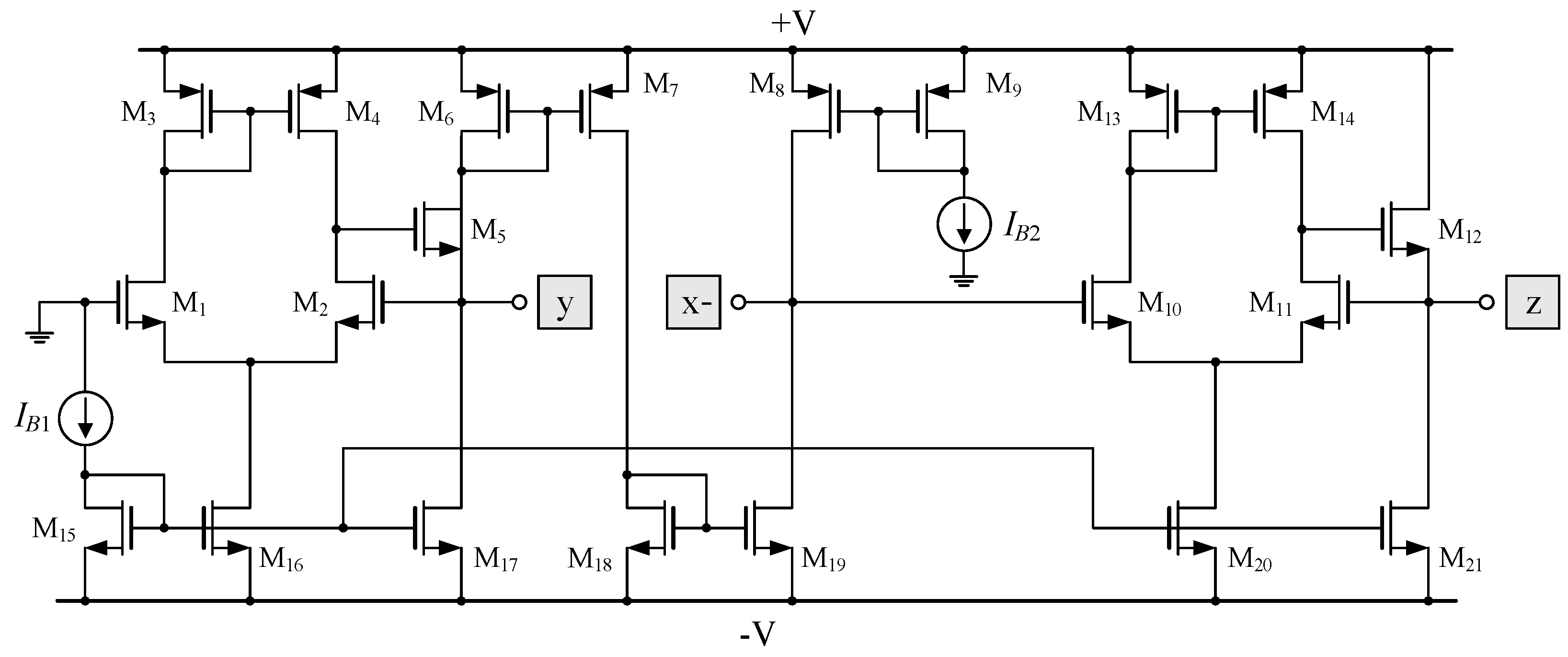
| Transistors | W/L (μm/μm) |
|---|---|
| M1 - M2, M10 - M11 | 10/0.18 |
| M3 - M4, M6 - M7, M8 - M9, M13 - M14 | 5/0.18 |
| M5, M12 | 50/0.18 |
| M15 - M21 | 3/0.18 |
Disclaimer/Publisher’s Note: The statements, opinions and data contained in all publications are solely those of the individual author(s) and contributor(s) and not of MDPI and/or the editor(s). MDPI and/or the editor(s) disclaim responsibility for any injury to people or property resulting from any ideas, methods, instructions or products referred to in the content. |
© 2025 by the authors. Licensee MDPI, Basel, Switzerland. This article is an open access article distributed under the terms and conditions of the Creative Commons Attribution (CC BY) license (http://creativecommons.org/licenses/by/4.0/).


