Submitted:
07 January 2025
Posted:
07 January 2025
You are already at the latest version
Abstract
In this paper, the relationship between GaN exciton energy and temperature was studied with high-quality and strain-free GaN epilayers. The traditional Varshni’s model and Bose-Einstein model are empirical models that lack consideration of physical mechanisms, which makes their models have poor applicability in wide band gap materials. Consider the interaction of electrons and phonons, we use singular functions, linear functions and power functions to express the phonon density of GaN, 2BE, single-linear, power-law-delta and power-law-v models are proposed. All of them are fitting well with the experimental data. Among them, the singular-linear model summarizes the contributions of acoustic phonon and optical phonon. The error of sigular-liner model is smaller than that of 1BE and varshni models in almost the whole temperature range.Therefore, the singular-linear model is better choices.
Keywords:
GaN
; exciton energy
; temperature
; modes
1. Introduction
In recent decades, many groups have studied related research on the relationship between the energy bands of semiconductor materials and temperature[1,2,3,4,5]. These studies can help us to have an accurate understanding of the dependence of energy band on temperature which is precisely an important prerequisite to correctly understand the optical and electrical properties of semiconductor materials. At present, for those traditional materials, such as Si, Ge, GaAs, InP etc, many groups have systematically studied the dependence of their exciton energy on temperature and have achieved great results[6,7,8,9,10,11]. However, over the years, in the field of wide band gap semiconductor materials, especially for GaN materials, high quality GaN samples cannot be obtained due to the lack of effective preparation methods. Therefore, there is no way for us to carry out systematic scientific research and naturally there is no definitive conclusion. In recent years, fortunately, the rapid development of MBE and MOCVD growth technologies has enabled us to produce high-quality GaN, which provides the basis for our research on GaN. This article will systematically study the dependence of GaN exciton energy on temperature.
For the behavioral pattern of exciton energy with temperature, it is commonly recognized that exciton energy has quadratic behavior at low temperatures, and has a linear progressive relationship at high temperatures[12,13]. In recent years, some groups have found that excitonic energy has a new behavioral pattern at low temperatures[14,15,16]. At a low temperature of 4K, the exciton energy of silicon has been found by a team to be mathematically related to the temperature being 4th power. For the factors that affect the exciton energy of semiconductor materials at ultra-low temperatures with temperature dependence, many groups have conducted detailed investigations and achieved some results[17].
2. Experiments
In order to obtain accurate band edge luminescence energy, it is necessary to eliminate material defects, internal strain and other factors which may affect the energy of the band edge, so high quality GaN epitaxial materials are indispensable. In this work, we use 400-μm thick freestanding GaN substrates to realize high-quality and strain-free GaN epilayers using metal organic chemical vapor deposition (MOCVD). It is well known that normal GaN grown on a sapphire substrate shows a dislocation density as high as 109/cm2. The GaN epilayer with no any heterostructure grown on the freestanding GaN substrate (GaN/GaN) give a great improvement on the crystal quality by the high-resolution XRD measurement, shown in Figure 1(a) (b). As a comparison, for a normal GaN layer grown on a sapphire substrate, the full width at half maximum (FWHM) of the (0002) diffraction peak is more than 400 arcseconds, and it is more than 600 arcseconds for (10-11) diffraction peak. However, for the GaN layer grown on the GaN substrate, the FWHM is only 62 arcseconds and 42 arcseconds for the corresponding diffraction peaks. The GaN/GaN sample shows extremely low dislocation density — as low as 105/cm2, as calculated from the high-resolution XRD results. Furthermore, Raman scattering measurement (not show here) proves that the GaN layer grown on the GaN substrate is totally strain free. Hall measurement shows very low unintentional doping concentration as low as 1015/cm3 in the high-quality GaN epilaye.
We performed PL measurement from 10 K to 250 K. The PL measurements are carried out through a 0.75 m monochromator and a low-temperature sample stage cooled by a Helium Closed Cycle Cryostat. The excitation source is a He-Cd laser with 325 nm which can be focused to a small area about 10 micrometer in diameter. Because the dislocation density of 105/cm2 is equivalent to an average distance of 30 micrometer between two adjacent dislocations, so the focus spot area is dislocation free with high possibility. The PL spectrum of the GaN/GaN sample is shown in Figure 2.
3. Calaultions and Modes
3.1. Early Modes
3.1.1. Varshini’s Mode
Referring to semiconductor exciton energy and temperature studies, we have to mention the earliest fitting formula Varshni’s formula. It is an approximate simulated model of the two behavioral models proposed by Varshni for the Eg-T curve at low and high temperatures. Since it was proposed, it is the most widely used energy band and temperature fitting formula for semiconductors. The fit is as follows[13,14,15,16,17,18]:
In the Equation (1), the parameter represents the exciton energy at 0K, and the parameter α is the energy band contraction coefficient at high temperature, or the slope of the fitted line at the time of high temperature fitting. The fitting result of the parameter β is widely considered to be related to the Debye temperature of the material studied. In the study of GaAs, the fitted parameter β represents its Debye temperature.
We first use the Varshni’s model to perform fitting studies on our data. The fitting results are shown in the solid black line in Figure 3(a). The results of the fitting parameters are shown in Table 1. From the figure, we can see that, in the lower temperature range below 60 K, and after the higher temperature range after 170 K, the fitting results are significantly smaller than the experimental data. In order to better analyze the difference between the fitting result and the experimental data, we make an illustration of Figure 3 according to the relationship between the difference between the experimental data and the fitting data and the change of temperature. It can be seen from the figure that the fitting data are all too small in the temperature range of 70K to 170 K. From the fitting pattern and fitting error results, we can see that the fitting results are systematic errors. In the study of non-wide band gap semiconductor materials, the Varshni’s formula has performed very well, but it has performed very poorly in wide band gap semiconductor materials such as GaN. As we see the fitting parameters in Table 1, the fitting result of α is 19, and the apparently abnormal number of is as high as 2509. By comparing past fitting results of Varshni’s formula to GaN, we find that there is a wide range of distribution of the fitting parameter α and β, and even negative numbers that are difficult to explain in terms of physical phenomena. Therefore, Varshni’s mode is not a suitable model to study the energy of GaN excitons. The reason we believe is its overly simple mathematical expression. Only three parameters with no actually physical meaning are insufficient to characterize the behavior of GaN excitons at low and high temperature. Secondly, the premise of the Varshni’s model is inconsistent with the actual situation.
3.1.2. Bose-Einstein Mode
Starting from the Bose-Einstein model, Vina proposed another alternative model. The fit is as follows[18,19]:
Another version of this formula can be obtained from Equation. The bandgap limit at T=0 is given by . α=2/θ is the contraction coefficient of the limit band gap, and θ represents the effective phonon temperature, which is related to the average frequency of the acoustic branch and the optical branch by.
From the result of Figure 3, there is a visible deviation from the temperature before 180K, and the illustration of the error analysis also proves this point. As with the Varshni‘s model, there is a systematic bias in certain temperature ranges. The fitting result of the model in the temperature section before 40K tends to be a stable trend, because when, there is a mathematical expression.
An overly simple mathematical design makes its fitting performance at low temperatures unreliable. The reason why the model performs well in the temperature range after 110 K is due to the fact that its physical parameters have a certain physical meaning. Therefore, the fitting parameters are more reasonable than the Varshni’s formula. However, in spite of this, from the perspective of the fitting effect R2, the formula proposed by Vina is still insufficient to describe the relationship between the exciton energy of GaN and temperature, and even worse than the Varshni’s formula. We need to proceed from the correct physical mechanism, select an appropriate number of parameters with physical meanings, establish a mathematical model, and develop the study of GaN exciton energy.
3.2. Novel Mode
Both the Varshni’s model and the Bose-Einstein model are empirical models that lack consideration of physical mechanisms, which makes their models have poor applicability in wide band gap materials. We know that starting from the physical mechanism, the energy band shifts with temperature due to two reasons: the thermal expansion of the lattice and the interaction of electrons and phonons. In general, the first reason contributes less, so we can ignore it, and the latter is the main influencing factor. We need to focus on consideration. From this point of view, a group has proposed such primitive integration[20]:
where is energy and is the average number of phonons or the probability of occupying phonons in the energy.,is the coupling coefficient of electron phonon interaction which is often summed up as a constant, and is the density of phonon states. For different semiconductor materials, it is important to properly mathematically represent the phonon density of states.
3.2.1. Singular Mode
A reasonable guess for density of phonon states in GaN materials is to use singular functions to generalize. When we use a singular function to express the phonon density of its acoustic phonons and optical phonons, that is,, the integral result is the Bose-Einstein model of (2). The fitting result of (2) is not ideal and reasonable. Then when we use two singular functions, andrepresent the phonon density at the low energy end and the high energy end, respectively. That is, substituting the original approximate integral result :
We call it 2BE model. In Equation (4), represents the band gap energy at 0K, α represents the high energy band shrinkage factor, and represent the effective phonon temperature of the acoustic branch and the optical branch respectively, and ω, 1-ω represents the acoustic branch and the optical Branches contribute to the band offset.
It can be seen from Figure 4(a) that the fitting curve of the 2BE model is closer to the experimental data than to the 1BE model which uses only a singular function for expression. The error analysis and comparison of the illustration also shows that the error of 2BE model is smaller than that of 1BE model in almost the whole temperature range, and is evenly distributed in the positive and negative range. There is no obvious system deviation. The fitting parameters and are 138 K and 645 K, respectively. It can be concluded that the effective energy of the acoustic phonon is 11.9 MeV and the energy of the optical phonon is 55.6 MeV. It can be seen that the phonon density of GaN is in reasonable range. The ω is 0.211, which means that in the variation of exciton energy of GaN with temperature, optical phonons play a major role. Better fitting patterns, smaller fitting errors, and fitting parameters with reasonable physical meanings indicate that the 2BE model has good performance for GaN E-T curve analysis.
3.2.2. Linear Mode
In addition to singular functions, we can consider using a linear function to mathematically express the density of phonon states, such assubstituting the original integral formula, and the integral approximation result is:
In Equation (5), represents the energy of excitons at 0K.α represents the contraction coefficient of the energy band at high temperature, and θ represents the effective phonon temperature. The result of fitting using Equation (5) is shown in Figure 5. The fitted result graph is very inappropriate. From the perspective of the entire fitting temperature range, there is a large error between the experimental data, and the magnitude of the parameters we fit out also cannot represent the physical meaning it represents. Therefore, simply using a linear function to summarize the density of phonon states of GaN does not achieve the desired fitting effect.
3.2.3. Power-Law Mode
In addition to linear functions, power functions are often used to describe the phonon density of semiconductor materials. In the study of exciton energy of other semiconductor materials, good results can be obtained. We describe the density of phonon states of GaN materials by constructing different power functions, and then make mathematical derivation, and use the resulting integral formula to fit the experimental data.
- (a)
- Power-law-delta mode
The density of phonon states of GaN is described in the form of , where , represents the cutoff energy, and the integration result in the energy range greater than is zero. Bring this equation to the integral approximation result:
In Equation (6),. , α, θ in the formula has the same physical meaning as before. Using Equation (6) to fit the experimental data, the fitting pattern of Figure 6 is obtained. It can be seen from the figure that the fitting data is closer to the experimental data. R2 as high as 0.9997 also means that the fit is very successful. The effective phonon temperature of 478.96 K and the phonon energy of 41.238 MeV are also in the reasonable energy range of the GaN phonon. This shows that the model can successfully perform mathematical analysis of the exciton energy of GaN and can obtain fitting parameters with reasonable physical meaning.
- (a)
- Power-law-v mode
In addition to the power function constructed above, we can also try to describe the phonon density of GaN in the form of. When certain conditions are satisfied, the integral approximation result can be:
Among them,, the condition to be satisfied is that p is less than 2.5. , α, θ have the same physical meaning.
The fitting result is shown in Figure 7. Obviously, the fitting effect is very good. From the fitting parameters, although the R2 value of 0.996 is appropriate, and the value also satisfies the approximate condition, the fitted α, θ values are all too large, especially the effective phonon temperature θ is as high as 1581 K. The phonon energy of 136 MeV is much larger than the phonon energy spectrum of GaN, and thus the fitted result does not represent the actual physical state of GaN. The description of the phonon density of states does not provide a good summary of the actual phonon density of GaN.
3.2.4. Singular-Linear Mode
Although neither the singular function nor the linear function is sufficient to describe the phonon density of GaN individually, we can still see some reasonableness of them. Then we can give full play to their respective rationality and combine them to describe the phonon density of GaN. Takeas an example, where the first term represents the low-end contribution of the acoustic phonon and the second term represents the contributions of acoustic phonon of high-energy end and optical phonon. The approximate integration results is:
where, α has the same physical meaning. Effective phonon temperature is represented by, where ω represents the weight of the contribution.
It can be seen from Figure 8 that its fitting effect is good。ω = 0.465, indicating that the phonon contribution at the low energy end is less, compared with the 0.211 contribution weight of the 2BE model, which is a little larger, but it still shows that the high energy terminator plays a major role. From θ=711 K, the effective phonon temperature is 546 K, and the effective phonon energy is 47 MeV. This is within the range of high-energy and low-energy phonons. This shows that the singular-line model can be applied in the exciton study of GaN materials.
4. Discussion
Experiments with various models allowed us to find a mathematical model that properly studied the relationship between GaN exciton energy and temperature. We found that mathematical models with 4 or even more parameters have better applicability than that with 3 parameters. This is because there are two types of behavioral patterns of exciton energy with temperature .At low temperature, owing linear behavior, and at high temperature, appearing the behavior of 2nd power, where characterize two behavior patterns as four independent variables. Of course, more parameters with physical and mathematical significance will be better, but this requires more experimental data to fit. In addition, the thermal expansion of the lattice is a problem that we need to consider. It is the secondary factor affecting energy band shift with temperature. As the temperature gets higher, its contribution weight will continue to increase, so that we need to consider the point. We did not consider its influence when we started from the physical mechanism, but we still constructed a good model and fitted out the parameters with physical meaning. This is because the thermal expansion of the lattice is mainly caused by the LA phonons, so we are considering the interaction of phonons with electrons. Among the mathematical terms in the fitting process, there is the influence of lattice thermal expansion. Therefore, we do not need to consider the influence of thermal expansion of the lattice additionally, which will increase the complexity of the fitting formula and the requirement for experimental data volume. Figure 9 shows the comparison of the error between the fitting results of Equation (1), (2), (4), (6), (7), and (8) and the experimental data at different temperatures. The error analysis shows that the error of 2BE, power-law-delta, power-law-v and sigular-liner models are smaller than that of 1BE and varshni models in almost the whole temperature range. Two singular functions are used in 2BE model and in the variation of exciton energy of GaN with temperature, optical phonons play a major role. The singular function and the linear function are used in sigular-liner mode, which contain low-end contribution of the acoustic phonon, contributions of acoustic phonon of high-energy end and optical phonon.
5. Conclusions
Based on the above data fittings and analysis, we can find that in all the fitting methods, 2BE, power-law-delta, power-law-v, and single-linear models are all on the fitting pattern. It can be fine satisfied, but the reasonableness of the fitting parameters does not fully satisfy our reasonable requirements. The 2BE model mainly summarizes the role of optical phonons. Meanwhile, we can see that the power-law-v model fitting parameters are not self-consistent. The power-law-delta model does not allow us to see high-energy and low-energy phonon pairs when we need to obtain information about the ratio of their contribution to energy band changing with temperature. Compared to them, the singular-linear model summarizes the role of optical phonons and acoustic phonon. For this reason, the singular-linear model is better choice.
Author Contributions
Conceptualization, P.C.; formal analysis, X.L.; methodology, X.L., Z.X., D.C.,X.X and H.Z ; software, X.L., and; investigation, P.C.; resources, P.C.; data curation, P.C.; writing—original draft preparation, P.C.; writing—review and editing, P.C.; supervision, Y.S.,R.Z. and Y.Z; project administration, P.C.; funding acquisition, P.C. All authors have read and agreed to the published version of the manuscript.
Funding
This research was funded by National Nature Science Foundation of China, grant number 12074182, Collaborative Innovation Center of Solid-State Lighting and Energy-saving Electronics and Open Fund of the State Key Laboratory on Integrated Optoelectronics, grant number IOSKL2017KF03.
Data Availability Statement
All data, theory detail, simulation detail that support the findings of this study are available from the corresponding authors upon reasonable request.
Acknowledgments
The authors acknowledge Nanjing University and Jiangsu Provincial Key Laboratory of Advanced Photonic and Electronic Materials for their support in advanced micro technology and clean room facilities.
Conflicts of Interest
The authors declare no conflict of interest.
References
- Boutramine, A. Temperature-and Composition-Dependent Band Gap Energy and Electron–Phonon Coupling in InAs1−xSbx Semiconductors Alloys for Infrared Photodetection. Journal of Electronic Materials 2023, 52, 6031-6041. [CrossRef]
- Isik, M.; Gasanly, N. M.; Darvishov, N. H. and Bagiev, V. E. Effect of temperature on band gap of PbWO4 single crystals grown by Czochralski method. Physica Scripta 2022, 97, 45803. [CrossRef]
- Kumar, A.; Kumar, S.; Miyai, Y. and Shimada, K. Temperature-dependent band modification and energy dependence of the electron-phonon interaction in the topological surface state on Bi2Te3. Physical Review B 2022, 106, 121104. [CrossRef]
- Surucu, O.; Isik, M.; Terlemezoglu, M.; Bektas, T.; Gasanly, N. M. and Parlak, M. Temperature effects on optical characteristics of thermally evaporated CuSbSe2 thin films for solar cell applications. Optical Materials 2022, 133, 113047. [CrossRef]
- Wu, R.; Ma, M.; Zhang, S.; Zhao, P.; Li, K.; Zhao, Q.; Chang, A. and Zhang, B. Enhanced linearity of CaCu3Ti4O12 by changing energy band structure induced by Fe3+ doping for high temperature thermistor application. Applied Physics Letters 2022, 121, 96124. [CrossRef]
- Allen, P. B. and Cardona, M. Temperature dependence of the direct gap of Si and Ge. Physical Review B 1983, 27, 4760-4769. [CrossRef]
- Hartel, A. M.; Gutsch, S.; Hiller, D. and Zacharias, M. Fundamental temperature-dependent properties of the Si nanocrystal band gap. Physical Review B 2012, 85, 165306. [CrossRef]
- Klenner, M.; Falter, C. and Ludwig, W. Temperature dependence of band gaps in Si and Ge in the quasi-ion model. Annalen der Physik 2006, 504, 34-38. [CrossRef]
- Lautenschlager, P.; Allen, P. B. and Cardona, M., Temperature dependence of band gaps in Si and Ge. Physical Review B 1985, 31, 2163-2171. [CrossRef]
- Vainorius, N.; Kubitza, S.; Lehmann, S.; Samuelson, L.; Dick, K. A. and Pistol, M.-E. Temperature dependent electronic band structure of wurtzite GaAs nanowires. Nanoscale 2018, 10, 1481-1486. [CrossRef]
- Pavesi, L.; Piazza, F.; Rudra, A.; Carlin, J. F. and Ilegems, M. Temperature dependence of the InP band gap from a photoluminescence study. Physical Review B 1991, 44, 9052-9055. [CrossRef]
- Vasileff, H. D. Electron Self-Energy and Temperature-Dependent Effective Masses in Semiconductors:n-Type Ge and Si. Physical Review 1957, 105, 441-446. [CrossRef]
- Pssler, R. Basic Model Relations for Temperature Dependencies of Fundamental Energy Gaps in Semiconductors. physica status solidi (b) 1997, 200, 155-172. [CrossRef]
- Uesugi, K.; Suemune, I.; Hasegawa, T.; Akutagawa, T. and Nakamura, T. Temperature dependence of band gap energies of GaAsN alloys. Applied Physics Letters 2000, 76, 1285-1287. [CrossRef]
- Pässler, R. Temperature dependence of fundamental band gaps in group IV, III–V, and II–VI materials via a two-oscillator model. Journal of Applied Physics 2001, 89, 6235-6240. [CrossRef]
- Zardas, G. E.; Yannakopoulos, P. H.; Ziska, M.; Symeonides, C.; Vesely, M. and Euthymiou, P. C. Temperature dependence of Si–GaAs energy gap using photoconductivity spectra. Microelectronics Journal 2006, 37, 91-93. [CrossRef]
- Pässler, R. Temperature dependence of exciton peak energies in multiple quantum wells. Journal of Applied Physics 1998, 83, 3356-3359. [CrossRef]
- Viña, L.; Logothetidis, S. and Cardona, M. Temperature dependence of the dielectric function of germanium. Physical Review B 1984, 30, 1979-1991. [CrossRef]
- Pässler, R. Alternative analytical descriptions of the temperature dependence of the energy gap in cadmium sulfide. physica status solidi (b) 2006, 193, 135-144. [CrossRef]
- O’Donnell, K. P. and Chen, X. Temperature dependence of semiconductor band gaps. Applied Physics Letters 1991, 58, 2924-2926. [CrossRef]
Figure 1.
Comparison of crystal quality between GaN/sapphire and GaN/GaN by high-resolution XRD measurement (a)(0002)ω scan (b) (10-11)ω scan.
Figure 1.
Comparison of crystal quality between GaN/sapphire and GaN/GaN by high-resolution XRD measurement (a)(0002)ω scan (b) (10-11)ω scan.
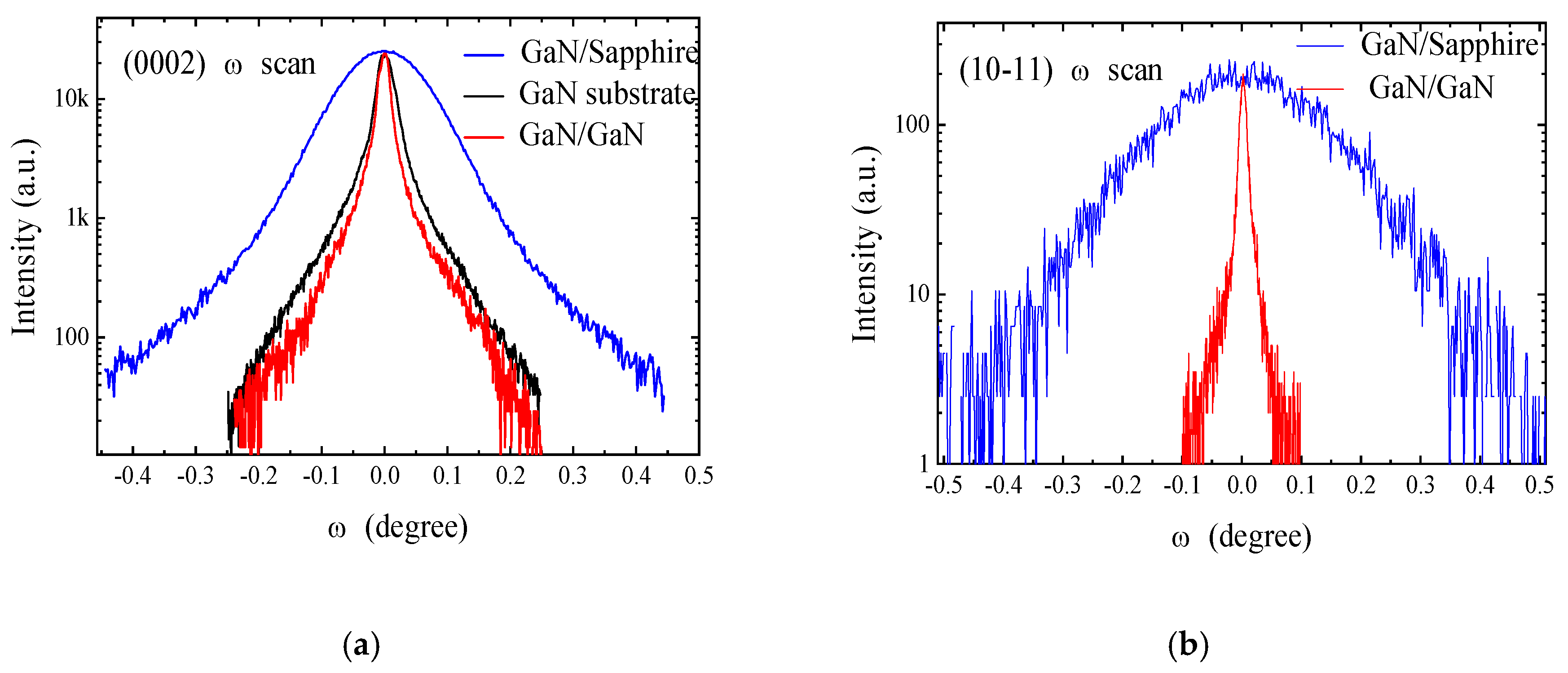
Figure 3.
(a) Comparison of the fitting results of the A free exciton energy of GaN materials using Equations (1) and (2) in the temperature range of 0K-230K. The straight line in the figure is the high temperature limit of the type 2 line. The straight line passes Eg (0), and the cross mark represents the feature point (T=θ/2). The black dots are the experimental data, and the black curved line is the fitting result of Equation (1). The red dashed line is the fitting result of Equation (2). The (b) shows the errors of the fitting results of Equations (1) and (2) compared with experimental data at different temperatures. The red circle represents the error of Equation (1), and the square black box represents the error of Equation (2). The ordinate represents the difference between the experimental data and the fitted data.
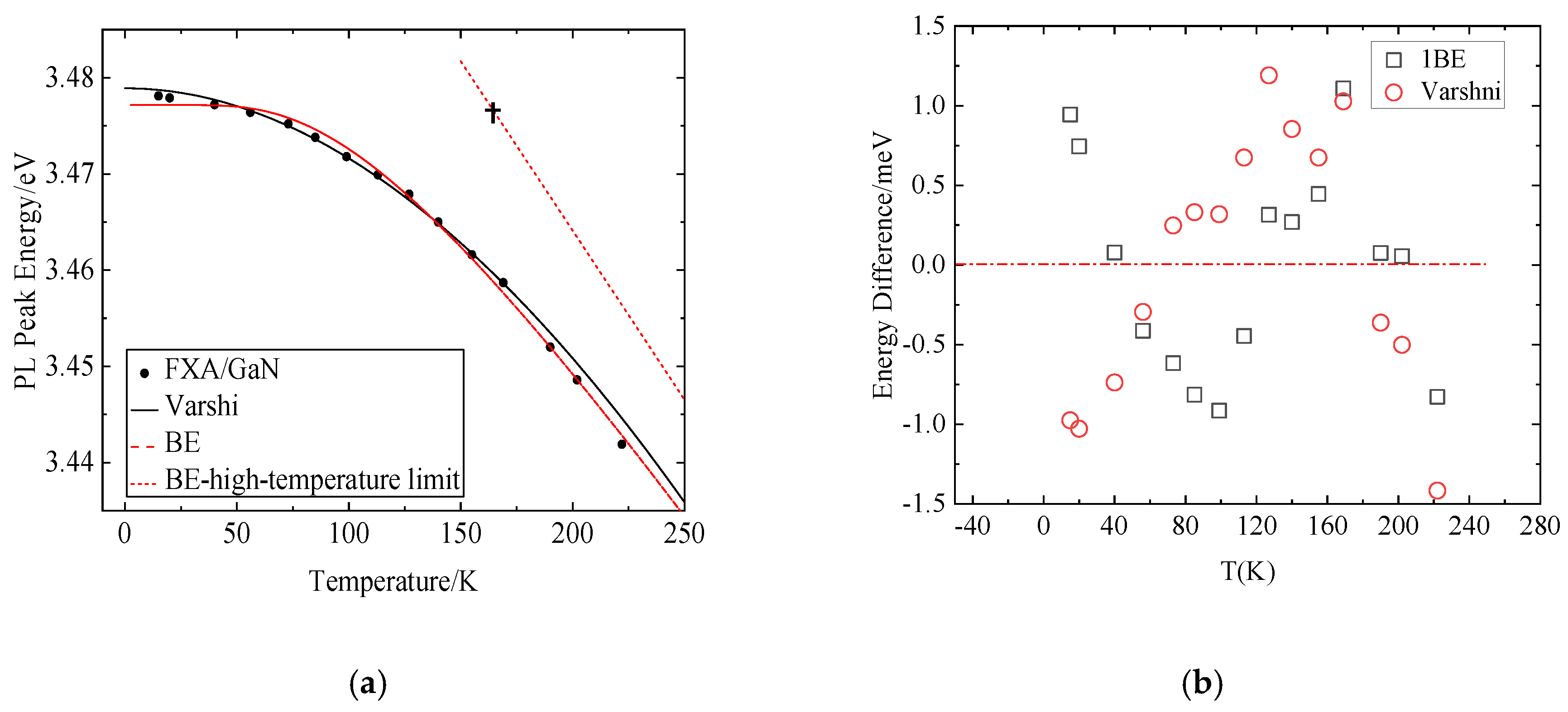
Figure 4.
(a) Comparison of the fitting results of 1BE and 2BE to GaN materials. The red curve in the figure is the fitting result of 1BE, and the blue curve is the fitting result of 2BE. Black dots are experimental data. (b) shows the error comparison between the fitted data and the experimental data for 1BE and 2BE. The ordinate represents the difference between the experimental data and the fitted data. The red dots indicate the error of the 1BE model, and the black squares indicate the error of 2BE.
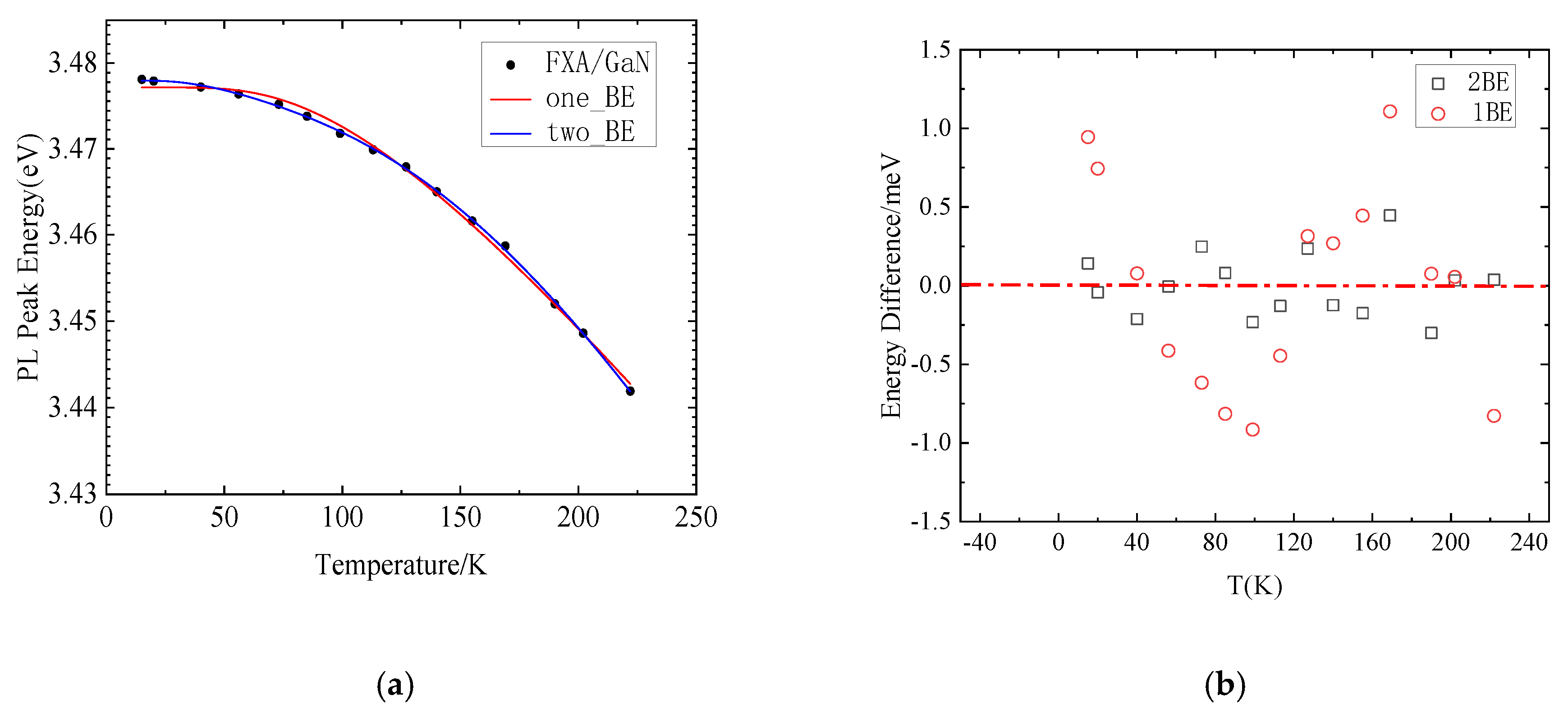
Figure 5.
Fit the experimental data using a linear model. Black dots represent the actual measured experimental data, and red solid lines represent the fitted curves.
Figure 5.
Fit the experimental data using a linear model. Black dots represent the actual measured experimental data, and red solid lines represent the fitted curves.
Figure 6.
The results obtained by fitting the experimental data to the power-law-delta model. The black dots represent the experimental data actually measured, and the solid red lines represent the fitted curves.
Figure 6.
The results obtained by fitting the experimental data to the power-law-delta model. The black dots represent the experimental data actually measured, and the solid red lines represent the fitted curves.

Figure 7.
The power-law-v model fitted to experimental data. The black dots represent the experimental data actually measured, and the solid red line represents the fitted curve.
Figure 7.
The power-law-v model fitted to experimental data. The black dots represent the experimental data actually measured, and the solid red line represents the fitted curve.
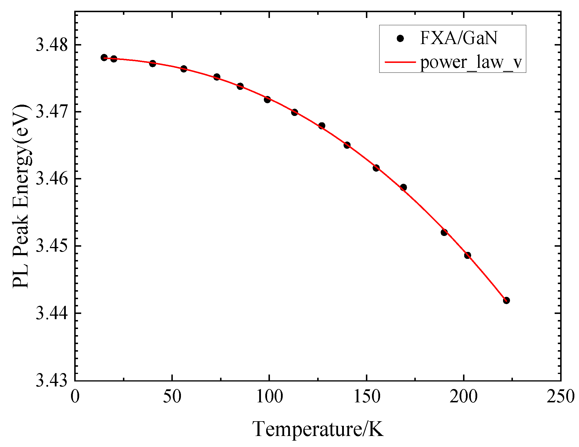
Figure 8.
The resulting plot of a singular-linear model fitted to experimental data. Black dots represent the experimental data actually measured. The solid red line represents the fitted curve.
Figure 8.
The resulting plot of a singular-linear model fitted to experimental data. Black dots represent the experimental data actually measured. The solid red line represents the fitted curve.
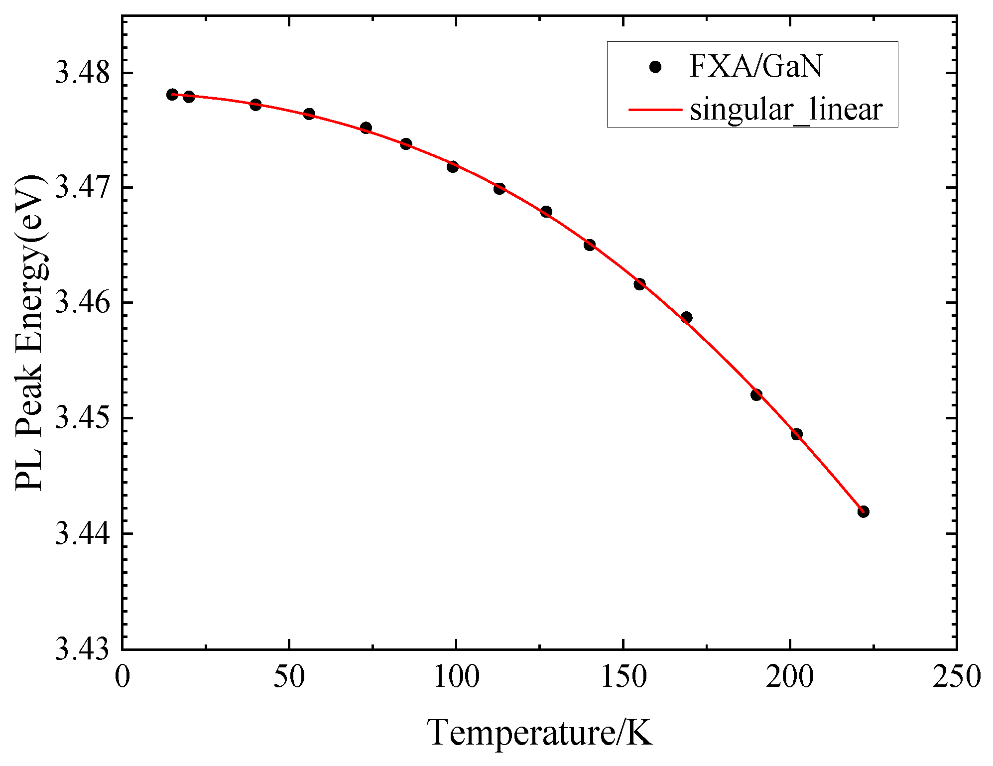
Figure 9.
The figure shows the comparison of the error between the fitting results of Equation (1), (2), (4), (6), (7), and (8) and the experimental data at different temperatures. The ordinate represents the difference between the experimental data and the fitted data.
Figure 9.
The figure shows the comparison of the error between the fitting results of Equation (1), (2), (4), (6), (7), and (8) and the experimental data at different temperatures. The ordinate represents the difference between the experimental data and the fitted data.
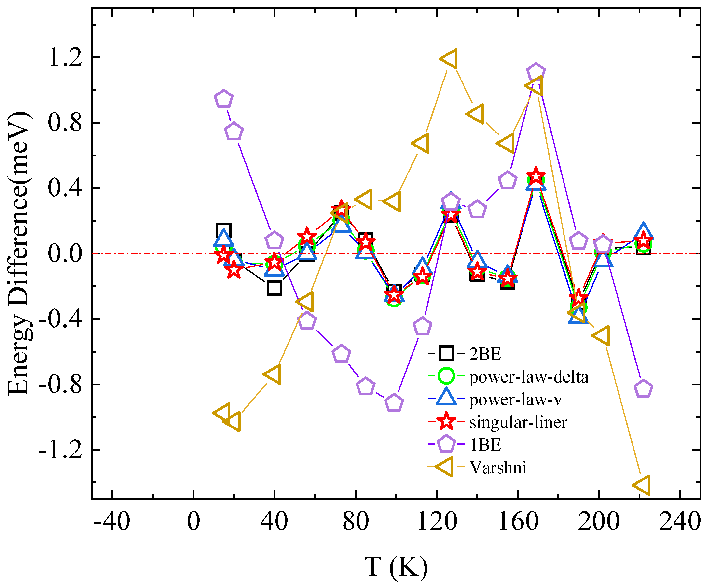

Table 1.
Parameters fitted to each mode.
| P/r/ | |||||||
| (1) | 3.4789 | 19 | 2509 | 216.2 | 0.996 | ||
| (2) | 3.47716 | 3.52 | 325.94 | 27.99 | 0.993 | ||
| (4) | 3.47779 | 5.7 | 138 | 645 | 0.211 | 0.9995 | |
| (6) | 3.478 | 5.7 | 478.96 | 0.46559 | 41.238 | 0.9997 | |
| (7) | 3.47809 | 18 | 1581 | 2.24 | 136.124 | 0.9996 | |
| (8) | 3.47825 | 5.8 | 711 | 0.465 | 0.9996 |
Disclaimer/Publisher’s Note: The statements, opinions and data contained in all publications are solely those of the individual author(s) and contributor(s) and not of MDPI and/or the editor(s). MDPI and/or the editor(s) disclaim responsibility for any injury to people or property resulting from any ideas, methods, instructions or products referred to in the content. |
© 2025 by the authors. Licensee MDPI, Basel, Switzerland. This article is an open access article distributed under the terms and conditions of the Creative Commons Attribution (CC BY) license (http://creativecommons.org/licenses/by/4.0/).
Copyright: This open access article is published under a Creative Commons CC BY 4.0 license, which permit the free download, distribution, and reuse, provided that the author and preprint are cited in any reuse.


