
Submitted:
03 January 2025
Posted:
06 January 2025
You are already at the latest version
Abstract
The Serial Peripheral Interface (SPI) protocol plays a crucial role in wearable and IoT devices, enabling high-speed communication between microcontrollers and peripherals such as sensors, displays, and connectivity modules. With the increasing complexity of modern devices and System-on-Chip (SoC) designs, robust verification methods are essential to ensure functionality and reliability. This paper utilizes Universal Verification Methodology (UVM) to develop a scalable and reusable testbench for SPI verification. The process encompasses test planning, simulation, emulation, and top-level verification to validate scenarios like multi-slave coordination and error handling. The results demonstrate the critical importance of UVM in ensuring the performance and dependability of SPI in advanced electronics, contributing to the reliable integration of the protocol in future devices.
Keywords:
serial peripheral interface
; universal verification methodology
; functional verification
; IoT devices
; system-on-chip
1. Introduction
The Serial Peripheral Interface (SPI) protocol is a cornerstone of modern electronic systems, widely used in wearable devices and IoT applications[1] due to its high-speed, full-duplex communication capabilities[2]. Its architecture offers simplicity and flexibility, enabling seamless data exchange between microcontrollers and peripherals such as sensors, displays, and memory modules. In wearable gadgets like smartwatches and fitness trackers, SPI facilitates integration with heart rate sensors, accelerometers, and gyroscopes, allowing real-time data acquisition and GUI interactions[3]. The protocol’s configurability, combined with its ability to support multiple slave devices, makes it indispensable in IoT applications, including home automation systems[4], where it manages communication between microcontrollers, environmental sensors, and connectivity modules such as Zigbee or Wi-Fi[5,6].
As electronic products become increasingly complex, the SPI protocol’s role extends beyond simple device interconnectivity. It is now integral to highly sophisticated systems on chips (SoCs)[8] that power advanced wearable and IoT devices. The SPI protocol is a widely adopted synchronous communication standard, particularly in embedded systems, wearables, and IoT devices. It offers several advantages, such as full-duplex communication, a flexible data transfer width (up to 128 bits), and configurable clock edge timing for data transfer, making it well-suited for low to medium throughput applications[9]. SPI operates at lower speeds than high-bandwidth protocols like HDMI or DisplayPort[10], which are typically used for tasks requiring high data throughput, such as video streaming. SPI’s strengths lie in its ability to efficiently handle communication between a master device and multiple slave devices, making it ideal for simpler systems where high-speed video or audio transfer is not required. It can interface with storage devices (e.g., flash memory) and sensors, providing a reliable link for low-bandwidth data exchange. In the context of wearable devices and IoT systems, SPI facilitates communication between microcontrollers and peripherals, including sensors, displays, and wireless modules. While SPI is not suitable for high-throughput video transmission, it is commonly used for smaller displays in wearables and for transferring data to and from memory modules that may handle encryption internally. Thus, SPI continues to be a fundamental protocol for low-power, cost-effective systems in various consumer electronics.[11,12,16]
Universal Verification Methodology (UVM) plays a pivotal role in addressing this challenge, providing a robust framework for verifying the functionality of SPI-based systems. UVM not only enhances the confidence in design correctness but also ensures scalability and reusability in verification environments[7,14]. By adopting UVM, engineers can construct modular testbenches that simulate a wide range of operational scenarios, effectively uncovering potential issues in SPI communication at an early stage. This becomes increasingly critical as wearable devices and IoT systems integrate more sensors, connectivity options, and processing capabilities.
In this study, the functional verification of an SPI protocol is approached through a systematic design verification process under UVM. The methodology starts with test planning, where scenarios are outlined to cover all functional aspects, including error handling, multi-slave coordination, and edge-case performance. These scenarios are then implemented in a UVM testbench[15] and validated through simulation and emulation stages before progressing to top-level verification. This rigorous process ensures that the SPI implementation is robust and capable of performing reliably under real-world conditions.
The importance of this approach lies in its ability to address the increasing complexity of modern electronic designs. As wearable and IoT devices evolve, the demands on communication protocols like SPI escalate, necessitating a verification methodology that is both thorough and scalable.[16] By leveraging UVM, this research demonstrates a structured approach to verifying SPI functionalities, contributing to the development of reliable and efficient electronic systems.
2. Literature Review
2.1. Universal Verification Methodology on System-on-Chip
The adoption of Universal Verification Methodology (UVM) has become a cornerstone in hardware verification, particularly for modern, complex System-on-Chip (SoC) designs. UVM enables reusable and scalable verification frameworks, crucial for systems with intricate interactions and high-performance demands. For instance, the use of UVM in designing FPGA-based task schedulers optimized for real-time systems illustrates the methodology’s capacity to address latency and predictability issues in hardware systems[17]. By leveraging hardware-accelerated scheduling algorithms like Earliest Deadline First (EDF), researchers demonstrated significant reductions in task scheduling time, achieving better system reliability and resource utilization.
2.2. Coverage of the Verification
Functional verification continues to be a bottleneck in the semiconductor industry, consuming over 60% of the development time for ASIC and SoC designs. Existing UVM-based testbenches streamline this process by integrating coverage-driven functional verification, as showcased in verification environments for instruction cache controllers. These frameworks utilize agents, reference models, and scoreboards to ensure high coverage metrics, including code coverage above 99%[18]. Moreover, directed and random tests enhance the reliability of the verification process by uncovering edge-case scenarios. Advanced tools like SystemVerilog Assertions (SVA) have been pivotal in embedding temporal logic checks into these environments, further improving fault detection capabilities[19,20].
2.3. Verification with Artificial Intelligence
Recent advancements emphasize integrating artificial intelligence (AI) into UVM workflows to address verification scalability challenges. AI-driven methods, such as Convolutional Neural Networks (CNNs), optimize documentation parsing and test scenario generation, significantly reducing human intervention in repetitive tasks like test planning and debugging. For example, AI models trained on datasets derived from AMBA APB/AXI specifications showed high classification accuracy ( 98%)[21], outperforming traditional approaches like BERT[23,24,25] and TextConvoNet[26]. These systems categorize documentation into actionable and redundant segments, enabling faster protocol understanding and verification efficiency.
2.4. SPI under Wearable and IoT Devices
The SPI protocol is a pivotal communication standard widely used in wearable and Internet of Things (IoT) devices due to its efficiency in handling high-speed, low-latency data transfers. In wearable technologies like smartwatches and fitness trackers, SPI enables seamless integration with sensors such as heart rate monitors, accelerometers, and gyroscopes, allowing real-time data acquisition and interaction with graphical user interfaces. Its lightweight protocol and configurability are particularly advantageous in resource-constrained environments, ensuring minimal power consumption and efficient data handling. Similarly, home automation systems rely on SPI to connect microcontrollers with environmental sensors, connectivity modules like Zigbee or Wi-Fi, and actuators. SPI’s high data rates and ability to handle multiple slave devices make it an ideal choice for centralized control in smart home architectures. Furthermore, in applications like smart locks and security cameras, SPI facilitates rapid and secure memory access for logging and encryption. These versatile applications underscore SPI’s importance in creating robust, scalable, and responsive systems, solidifying its role in advancing the IoT and wearable sectors.[5,6]
3. Materials and Methods
3.1. Materials: What Should Be Tested in SPI and Take Care of
The SPI protocol is a highly versatile and efficient synchronous communication standard, well-suited for testing due to its full-duplex capabilities and support for flexible configurations. Its unique features, such as variable word lengths up to 128 bits, MSB/LSB-first data transmission, and edge-selectable data transfer, distinguish it from other protocols like I2C and UART. Unlike these protocols, SPI operates without addressing overhead, allowing for high-speed, low-latency communication. Additionally, the support for up to eight slave select lines makes it ideal for multi-device setups in modern embedded systems.
To test the SPI protocol, a combination of software and hardware resources will be utilized. This includes the development of a Universal Verification Methodology (UVM)-based testbench to simulate real-world operational scenarios. The testbench will interact with an SPI master implemented in Verilog, which will be synthesized and run on FPGA hardware to validate performance under actual conditions. The specification highlights that testing will involve verification of fundamental operations, such as full-duplex data transmission and configurable clock edge timing, alongside advanced configurations like multi-slave setups and variable character lengths.
3.2. Methods: Test Plan
A well-structured test plan is essential for verifying the functionality of the SPI protocol, especially when integrated into complex designs like wearable and IoT devices. The test plan ensures that all functional aspects of the protocol based on the Spec of the protocol[22], including communication integrity, edge cases, and control mechanisms, are systematically validated. Without a rigorous plan, it becomes challenging to ensure that SPI-based systems meet design specifications, particularly given the diverse configurations and applications highlighted in the SPI Master Core specification.
3.3. Methods: Designing the Test Plan
The testing process begins with setting up the SPI Master core using the specifications defined in the attached document. The system’s primary features, such as control registers and slave select lines, will be configured to match expected operational modes. A suite of targeted test cases will be executed, starting with basic functional tests, such as verifying the correct initialization and default behavior of the SPI core. More advanced scenarios, including multi-bit word transmission (8–128 bits) and edge-sensitive data transfer tests, will be conducted. Timing analyses will also be performed to confirm the clock divider’s accuracy under varying frequencies.
Additionally, error conditions, such as simultaneous multiple slave selection and misaligned clock settings, will be intentionally introduced to evaluate fault tolerance and error reporting capabilities. Hardware-in-the-loop (HIL) emulation using FPGA will validate the protocol’s behavior under physical constraints. By progressively increasing test complexity, the process ensures robust verification of SPI’s design while leveraging its unique characteristics for diverse embedded system applications.

Table 1.
Testplan design.
| Test Case ID | Description | Expected Outcome |
|---|---|---|
| No_01 | Validate SPI data transmission using default settings | Reliable communication between Master and Slave with default parameters |
| No_02 | Verify SPI clock divider operation across various divider configurations | SPI clock frequency aligns with the expected value for all divider settings |
| No_03 | Check data transfer in MSB-first format | Data is sent and received in MSB-first order |
| No_04 | Check data transfer in LSB-first format | Data is sent and received in LSB-first order |
| No_05 | Confirm full-duplex communication between MOSI and MISO | Both lines successfully transmit and receive data simultaneously |
| No_06 | Evaluate transmission with variable word lengths (8-bit, 16-bit, 32-bit, 64-bit) | Accurate data exchange across all specified word lengths |
| No_07 | Validate control register operations (e.g., GO_BSY, LSB, IE bits) | Control registers respond correctly when set or cleared |
| No_08 | Assess transmission functionality on rising clock edges for both MOSI and MISO | Data is correctly transmitted and received during rising clock edges |
| No_09 | Assess transmission functionality on falling clock edges for both MOSI and MISO | Data is correctly transmitted and received during falling clock edges |
| No_10 | Test compatibility with extended character lengths up to 128 bits | Accurate data transfer across character lengths up to 128 bits |
* Programmed under the SystemVerilog/UVM.
- Test Item Definition: Test items are defined to cover all possible scenarios, from basic data transmission to advanced functionalities. The provided test items, such as verifying MSB/LSB-first transmission, edge-based communication, and variable word lengths, ensure that all critical aspects of the protocol are tested. These test cases align with the SPI Master Core Specification, which allows flexible configurations like up to 128-bit data transfers, MSB or LSB-first settings, and edge-specific transmission.
- Test Case Prioritization: High-priority cases, such as basic transmission, serve as a foundation for testing more complex scenarios like variable word lengths and multi-character transmissions. This incremental approach minimizes the risk of overlooking fundamental issues.
- Simulation and Emulation: The testing methodology transitions from simulation to emulation for validating SPI under real-world conditions. Simulations are conducted at the register-transfer level (RTL) using models like UVM to verify logical functionality, while emulation replicates the behavior on physical hardware. This dual-layer approach ensures comprehensive coverage and identifies design flaws early in the process.
- Top-Level Verification: Finally, the entire SPI system is tested as part of a fully integrated design to validate interactions between subsystems. This phase confirms the protocol’s reliability under operational constraints typical of wearable and IoT environments.
3.4. Example Test Cases and Their Significance
3.4.1. Fundamental Operation: Ensuring That the Core Settings Perform as Expected
This step involves testing the basic functionality of the SPI controller core. The core should be able to transmit and receive data correctly under typical conditions, with the expected behavior when initialized. This validation checks whether the SPI controller operates as designed, without any errors or unexpected behavior, and that the settings such as baud rate, data format, and polarity are correctly configured and functioning.
3.4.2. Checks the Clock Divider’s Accuracy: SPI and External Peripherals’ Synchronization
The clock divider is a crucial component of the SPI system, as it divides the system clock to generate the SPI clock (SCK), which is used for data transmission. If the clock divider isn’t accurate, the timing between the SPI controller and the connected peripheral devices could be mismatched. This can result in communication errors or data corruption. Verifying the clock divider ensures that the SPI controller generates the correct clock speed that matches the timing requirements of the external device it is communicating with.
3.4.3. Behavior of Control Registers, Advanced Features
SPI communication often requires control over advanced features such as enabling interrupts (IE) or selecting specific slave devices (ASS, or Slave Select). The control registers configure the SPI controller’s operation for such features. Verifying these control registers ensures that:
- The interrupt functionality behaves as expected (triggering appropriate actions when specific conditions, like data ready or transmission complete, occur).
- The slave selection works properly, ensuring that the correct device (in a multi-slave configuration) is addressed when the SPI bus is used. This step is important for confirming that the more complex, advanced
- features of the SPI controller are operational and that the device interacts correctly with various external components or peripherals.
By following this structured methodology and referencing the SPI Master Core Specification, the test plan ensures robust verification of the SPI protocol, facilitating its reliable integration into sophisticated applications.
3.5. Importance of Sanity Testing in Verification
Sanity testing is indispensable in complex verification environments like SPI. By validating essential configurations and operational correctness in a controlled setup, it ensures that subsequent tests operate on a verified foundation. This reduces debugging time and enhances overall productivity. The spi_sanity_test serves this purpose by configuring and validating key SPI control registers, checking for protocol adherence, and confirming the proper functioning of the environment. Each register setting and phase in the code plays a crucial role in ensuring reliability and correctness during this process.
The use of a sanity test in SystemVerilog, particularly within a UVM (Universal Verification Methodology) framework, is critical in ensuring that the design under test (DUT) and the testbench environment are configured correctly before moving to more comprehensive testing. A sanity test validates the basic functionalities and confirms the setup’s correctness. In the context of a Serial Peripheral Interface (SPI) environment, this ensures that communication protocols, registers, and initial configurations behave as expected before progressing to more advanced and resource-intensive tests. The spi_sanity_test class in the code is designed as a foundational test, verifying the correctness of basic SPI settings and sequences, ensuring subsequent tests have a reliable starting point.
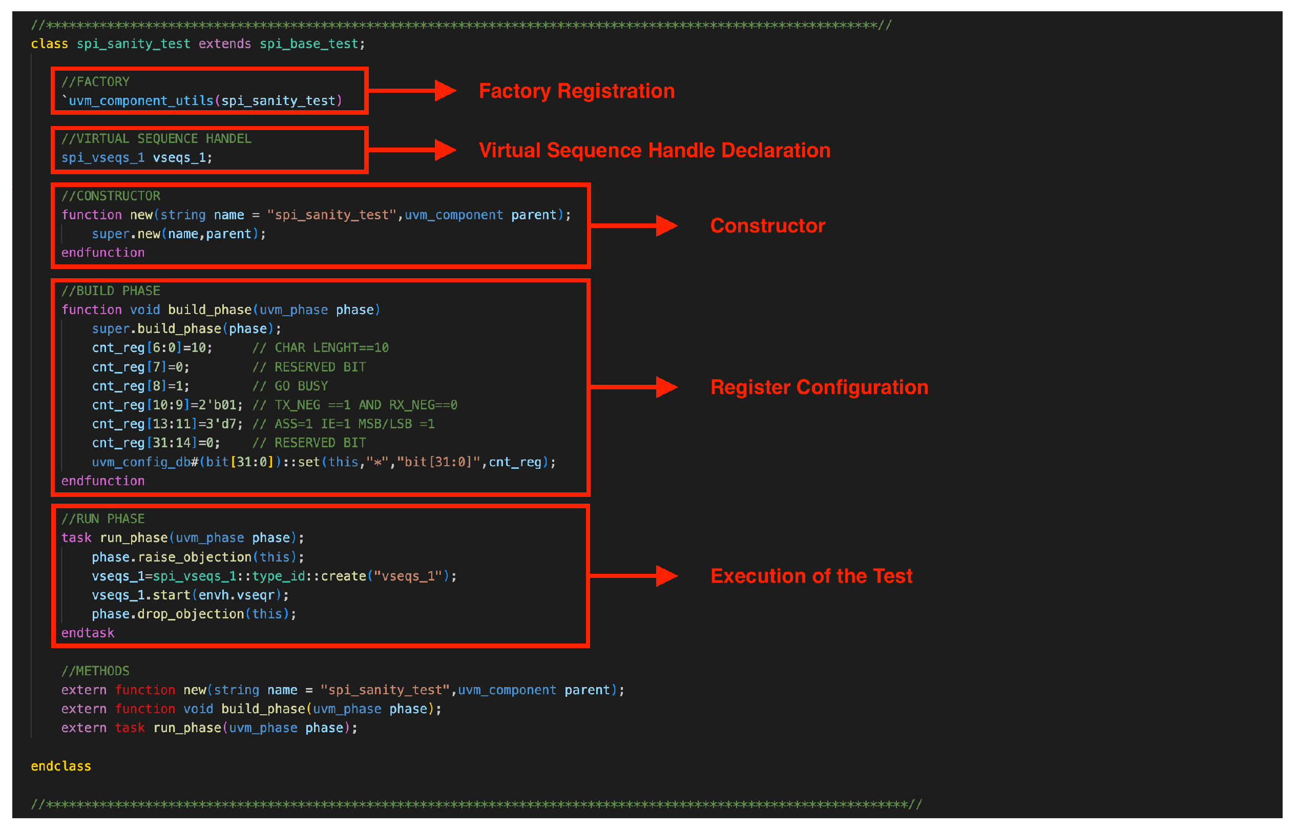
Figure 1.
Class spi_sanity_test in UVM, showcasing factory registration, virtual sequence handle declaration, constructor, register configuration in the build phase, and test execution in the run phase.
Figure 1.
Class spi_sanity_test in UVM, showcasing factory registration, virtual sequence handle declaration, constructor, register configuration in the build phase, and test execution in the run phase.
3.6. Breakdown of the Code: spi_sanity_test Class
3.6.1. Factory Registration
The uvm_component_utils macro registers the spi_sanity_test class with the UVM factory. This enables dynamic object creation and type-specific customization during runtime, a feature that is integral to UVM for scalability and reusability. Factory registration ensures that this test can be instantiated using the UVM type system, allowing configurations to be swapped dynamically without modifying the base testbench structure.
3.6.2. Virtual Sequence Handle Declaration
The vseqs_1 handle represents a virtual sequence (sequence driver for the testbench). It serves as an entry point to drive sequences that generate transactions on the DUT interface, ensuring abstraction between the test and the stimulus.
3.6.3. Constructor
The constructor initializes the class by invoking the base class’s new method with a default name (spi_sanity_test) and its parent. It adheres to UVM’s hierarchical component structure, ensuring modularity and consistency.
3.7. Build Phase: Register Configuration
The build_phase is a critical part of UVM where the testbench’s topology and default configurations are set up. For SPI, this involves defining specific control register (cnt_reg) values to initialize the SPI protocol.

Figure 2.
Detailed register configuration in the build_phase method, setting up the control register (cnt_reg) with specific bit-field values for SPI testing.
Figure 2.
Detailed register configuration in the build_phase method, setting up the control register (cnt_reg) with specific bit-field values for SPI testing.
- CHAR LENGTH (cnt_reg[6:0] = 10): This specifies the number of bits per transaction. A value of 10 indicates that each SPI transfer consists of 10 bits, a standard configuration for validating medium-length transfers during a sanity test.
- RESERVED BIT (cnt_reg[7] = 0): Reserved bits are set to 0 for consistency and to ensure no undefined behaviors in register configurations.
- GO BUSY (cnt_reg[8] = 1): The GO or BUSY flag signals the SPI interface to initiate a transfer. Setting this bit ensures that the SPI controller begins a transaction during the test.
- TX_NEG and RX_NEG (cnt_reg[10:9] = 2’b01): These bits control the data capture and transmission phase. Setting TX_NEG = 1 and RX_NEG = 0 configures the transmitter to change data on the falling edge and the receiver to sample data on the rising edge, a common configuration for SPI protocols.
-
ASS, IE, MSB/LSB (cnt_reg[13:11] = 3’d7):
- -
- ASS (Automatic Slave Select): A value of 1 ensures the chip select (CS) signal is managed automatically.
- -
- IE (Interrupt Enable): Enabling interrupts (IE = 1) ensures that any irregularities during communication are flagged immediately.
- -
- MSB/LSB: Setting this to 1 configures the SPI to transmit the most significant bit (MSB) first, which is standard for many SPI devices.
- RESERVED BITS (cnt_reg[31:14] = 0): Setting all unused bits to 0 prevents unintentional interference.
Finally, the uvm_config_db API is used to make this configuration accessible throughout the testbench.
3.8. Run Phase: Execution of the Test
The run_phase drives the test logic after the environment is constructed and configured:
Figure 3.
Run phase implementation, including objection handling and virtual sequence instantiation and execution for the SPI test.
Figure 3.
Run phase implementation, including objection handling and virtual sequence instantiation and execution for the SPI test.
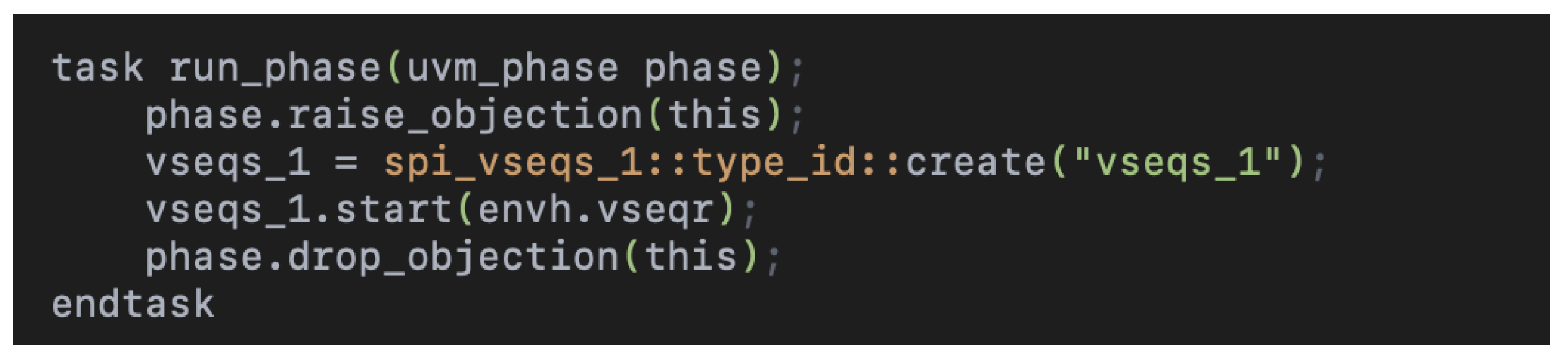
- Raise/Drop Objection: These methods synchronize the testbench phases. Raising an objection indicates that the test is still executing, while dropping it signals completion.
- Sequence Creation and Execution: The spi_vseqs_1 sequence is dynamically created and started on the virtual sequencer (envh.vseqr). This abstraction ensures that the generated transactions align with the defined protocol and environmental setup.
4. Results
4.1. Master and Slave Devices Under the Testbench
The results of the SPI protocol testing demonstrated successful data transmission between the master and slave devices, verifying the functionality and reliability of the system. The master device issued multiple requests (master_xtn) at different timestamps (9000ns, 15000ns, 21000ns, 27000ns, and 123000ns). Each request included key data elements such as address bits (ADDRESS BITS), output data (DATA_OUT), input data (DATA_IN), and control registers. The master driver’s log shows consistent updates to these fields, reflecting the correctness of data flow at each phase of the test. On the other hand, the slave device received and processed the transmitted data successfully. For instance, at 109000ns, the slave monitor captured the request (slave_xtn) with integral fields for MISO and MOSI. The transmission data integrity and timing accuracy observed in these exchanges validate the robust synchronization between master and slave devices.
Figure 4.
Log of the master driver displaying register and transaction states at 123000ns. The DATA_IN value was recorded as 2456940507, while DATA_OUT, CONTROL STATUS REG, and TX registers remained consistent. These results validate the driver’s correct operation in managing SPI transactions.
Figure 4.
Log of the master driver displaying register and transaction states at 123000ns. The DATA_IN value was recorded as 2456940507, while DATA_OUT, CONTROL STATUS REG, and TX registers remained consistent. These results validate the driver’s correct operation in managing SPI transactions.

4.2. Monitor and Driver Devices Under the Testbench
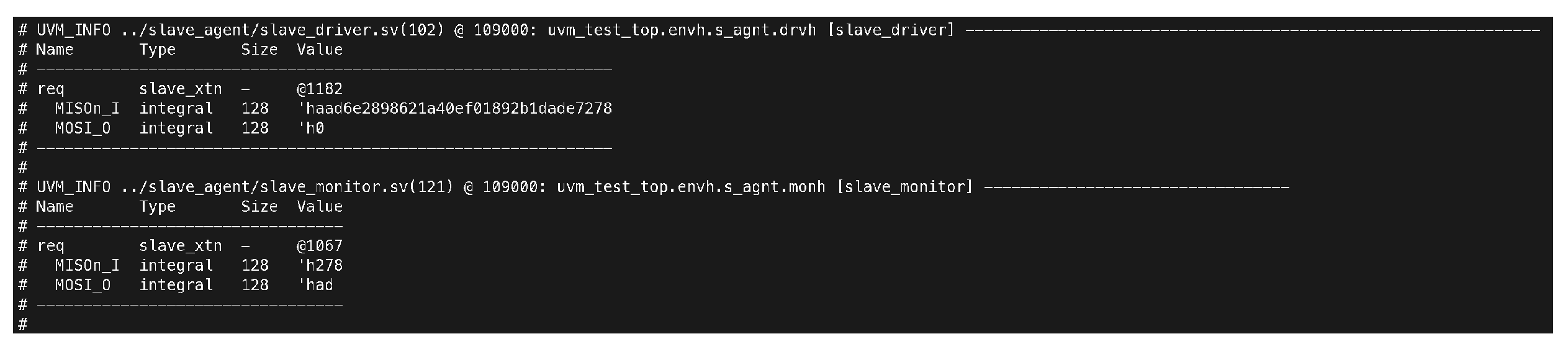
The monitoring components of the SPI system, particularly the master and slave monitors, provided detailed insights into data transmission. They captured the exact values of the transmitted and received data, ensuring accuracy in reporting and verifying system behavior. For example, the master monitor at 123000ns reported a DATA_IN value of 2456940507 and a CONTROL STATUS REG value of 15114, indicating proper processing of control and data signals. Additionally, comparisons of received and transmitted data in the log files revealed consistent alignment between expected and actual values. The test outcomes further highlight that the characters’ length was correctly set to 10 bits, with MOSI (Master Out Slave In) data recorded as 123 and MISO (Master In Slave Out) data as 798, matching the expectations for successful SPI communication.
Figure 5.
Log output from the master monitor capturing detailed register states at 123000ns. Key data includes DATA_IN set to d0, CONTROL STATUS REG set to d15114, and TX-0 REG represented as b1111011. These values confirm proper master-side data monitoring during SPI communication.
Figure 5.
Log output from the master monitor capturing detailed register states at 123000ns. Key data includes DATA_IN set to d0, CONTROL STATUS REG set to d15114, and TX-0 REG represented as b1111011. These values confirm proper master-side data monitoring during SPI communication.
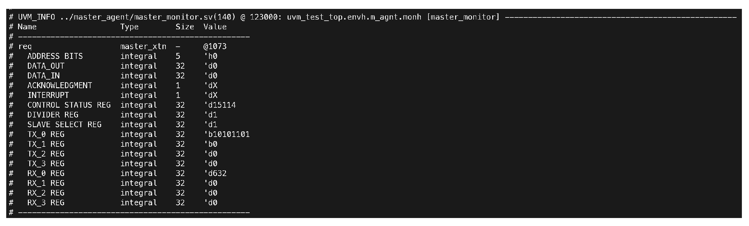
Figure 6.
Snapshot of the slave driver and monitor logs showing the captured MISO and MOSI data. The slave driver received a MISO value of he37e64871581d6a68e5df96946a26b1e and transmitted a MOSI value of h0. The slave monitor observed a MISO value of h31e and MOSI value of h7b at 109000ns.
Figure 6.
Snapshot of the slave driver and monitor logs showing the captured MISO and MOSI data. The slave driver received a MISO value of he37e64871581d6a68e5df96946a26b1e and transmitted a MOSI value of h0. The slave monitor observed a MISO value of h31e and MOSI value of h7b at 109000ns.
4.3. Waveform Demonstration on Result
The waveform illustrates a detailed sequence of SPI transactions between the master and slave devices. Key signals such as wb_clk_i, wb_rst_i, mosi_pad_i, and miso_pad_i are well-synchronized, indicating robust clock-domain crossing and data integrity throughout the communication. Address (wb_adr_i) and data (wb_dat_i) buses reflect precise transactions at designated clock cycles, ensuring accurate data handshaking between components. For example, the transitions in wb_ack_o and wb_err_o validate proper acknowledgment mechanisms and error-free communication. Furthermore, the sequence transitions in control signals such as wb_we_i, wb_stb_i, and wb_cyc_i demonstrate an effective write and read operation workflow. The miso_pad_i and mosi_pad_o signals exhibit consistent data flow in accordance with the SPI protocol, further validating the design’s adherence to specification.
Figure 7.
Waveform depicting SPI transactions, showcasing synchronized clocking, data handshaking on wb_adr_i and wb_dat_i, and successful communication via mosi_pad_o and miso_pad_i signals, adhering to the SPI protocol specification.
Figure 7.
Waveform depicting SPI transactions, showcasing synchronized clocking, data handshaking on wb_adr_i and wb_dat_i, and successful communication via mosi_pad_o and miso_pad_i signals, adhering to the SPI protocol specification.
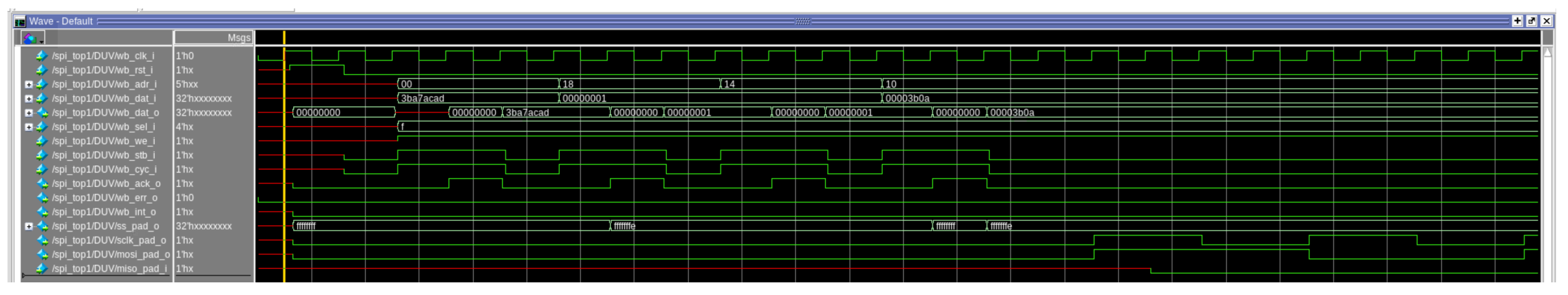
This waveform underscores the importance of employing UVM and SystemVerilog for such complex verification tasks. UVM provides a scalable and reusable verification framework, allowing for structured testbench development that facilitates debugging and analysis, as evident from the precise signal monitoring in the simulation. SystemVerilog enhances the verification process by offering advanced constructs for modeling, constrained-random testing, and functional coverage. Together, they empower engineers to identify intricate bugs and ensure protocol compliance effectively, reducing the risk of design flaws in real-world applications. This combination of tools is indispensable for modern hardware design and verification, ensuring high-quality, robust, and reliable system performance.
4.4. Coverage Analysis Summary
The coverage report for the SPI package demonstrates a robust verification process, achieving an overall instance coverage of 91.66%. The assertion coverage reached 100%, indicating that all specified assertions were effectively hit during simulation, ensuring key functional checks were comprehensively validated. The covergroup coverage, however, stands at 83.33%, revealing some room for improvement in exercising specific functional scenarios or corner cases. Additionally, the coverage for bins within the covergroups shows a rate of 87.5%, with one bin remaining unhit. This suggests that while the majority of the design’s functionality has been verified, additional test scenarios targeting unhit conditions could further enhance the thoroughness of the verification process. These results highlight the efficiency of the UVM-based verification environment, while also emphasizing the need for refining test coverage to achieve complete verification.
Figure 8.
Coverage analysis results for the SPI package, showing 91.66% overall instance coverage, 100% assertion coverage, 83.33% covergroup coverage, and 87.5% bin coverage, highlighting effective verification with opportunities for further improvement in specific scenarios.
Figure 8.
Coverage analysis results for the SPI package, showing 91.66% overall instance coverage, 100% assertion coverage, 83.33% covergroup coverage, and 87.5% bin coverage, highlighting effective verification with opportunities for further improvement in specific scenarios.

5. Discussion
The nuances of functional and code coverage underscore the complexity of verification tasks. While achieving functional coverage was a primary objective in this project, previous experiences, such as with a 1x3 router design, highlighted the importance of reaching 100% code coverage by exercising all lines, branches, and conditions in the HDL code. Nevertheless, code coverage and assertion coverage are complementary metrics—neither can fully guarantee design quality in isolation. For example, the functional suite successfully validated RX scenarios, but issues with TX bins revealed a potential RTL bug. Despite sequences covering all TX scenarios, specific bins remained unhit, emphasizing the importance of both metrics in identifying corner cases. Addressing such coverage gaps ensures a robust verification process and paves the way for improved hardware reliability.
5.1. Potential Areas for Improvement
- Additional Assertions: While the test effectively validates initial configurations and basic operation, it could benefit from assertions to monitor specific runtime conditions. For example, verifying that the GO BUSY flag clears after a transaction or that the MSB/LSB configuration aligns with transmitted data would enhance the test’s robustness.
- Coverage Metrics: The test does not explicitly mention functional coverage or code coverage metrics. Adding a coverage model that tracks key aspects, such as edge cases in character lengths or timing variations in TX/RX signals, would provide quantitative feedback on the test’s effectiveness.
- Error Injection: To further validate the SPI design, the test could introduce scenarios with intentional misconfigurations. For example, setting the reserved bits (cnt_reg[7] or cnt_reg[31:14]) to non-zero values could test the DUT’s resilience to unexpected inputs.
- Scalability to Larger Configurations: While the test focuses on a 10-bit character length, SPI designs often support configurable lengths (e.g., 8, 16, 32 bits). Expanding the test to dynamically handle multiple configurations would enhance its utility.
5.2. Educational Value and Industry Relevance
This implementation is highly relevant for students and professionals learning UVM and SPI protocols. It demonstrates practical applications of concepts like register configuration, virtual sequences, and phase synchronization. Moreover, SPI remains ubiquitous in applications ranging from embedded systems to high-speed communication interfaces. This test, therefore, provides a framework that is both educational and immediately applicable in industry settings.
The emphasis on clarity and explicit register settings ensures that even newcomers can grasp the key aspects of SPI operation. At the same time, the adherence to UVM best practices prepares users for more complex verification tasks.
6. Conclusions
The verification of the SPI protocol using Universal Verification Methodology (UVM) has proven to be a robust approach to ensuring the functionality and reliability of this critical communication protocol in modern IoT and wearable devices. By methodically covering key features such as full-duplex transmission, variable word lengths, and edge-sensitive data handling, this study demonstrated that the SPI protocol can meet the stringent demands of real-world applications. The results highlight comprehensive functional coverage and assertion coverage, validating the correctness of the SPI Master core under diverse scenarios, including high-speed data exchange and fault handling. This thorough verification process ensures the readiness of SPI for integration into application-specific integrated circuits (ASICs), which are essential for advanced wearable technology and IoT systems.
The spi_sanity_test is a well-crafted implementation that highlights the importance of early-stage validation in the verification process. Its detailed configuration and adherence to UVM principles make it a valuable resource for ensuring the reliability of SPI designs. While there are opportunities to expand its functionality, the test provides a solid foundation for both learning and professional use. By emphasizing clarity, modularity, and adherence to standards, it serves as an exemplary model for UVM-based verification in the context of SPI communication.
Wearable devices, in particular, demand precise, high-speed communication between microcontrollers and peripherals like sensors, displays, and connectivity modules. The application of UVM enables an efficient and scalable verification framework, reducing the time-to-market while maintaining the integrity of these intricate designs. This methodology not only ensures the quality of current ASIC implementations but also sets a standard for emerging technologies in embedded systems. The insights gained from this work lay a foundation for future research, including optimizing verification workflows for energy-efficient designs and exploring the application of UVM in other communication protocols, cementing its importance in the advancement of modern electronics.
Author Contributions
Funding
This research received no external funding.
Data Availability Statement
Not applicable.
Conflicts of Interest
The authors declare no conflict of interest.
Abbreviations
The following abbreviations are used in this manuscript:
| SPI | Serial Peripheral Interface |
| UVM | Universal Verification Methodology |
| IoT | Internet of Thing |
| RAL | Register Abstraction Layer |
| RTL | Register Transaction Level |
| DUT | Design Under Test |
References
- Dobrescu, C. C.; González, I.; Carneros-Prado, D.; Fontecha, J.; Nugent, C., "Direct Memory Access-Based Data Storage for Long-Term Acquisition Using Wearables in an Energy-Efficient Manner," Sensors, 2024, 24, 4982. [CrossRef]
- J. Chen and S. Huang, "Analysis and Comparison of UART, SPI and I2C," 2023 IEEE 2nd International Conference on Electrical Engineering, Big Data and Algorithms (EEBDA), Changchun, China, 2023, pp. 272–276, . [CrossRef]
- V. R. Kolagatla, A. Raveendran, and V. Desalphine, "A Novel and Efficient SPI enabled RSA Crypto Accelerator for Real-Time Applications," 2024 28th International Symposium on VLSI Design and Test (VDAT), Vellore, India, 2024, pp. 1–6, . [CrossRef]
- S. Mishra, A. Ray, M. Singh, S. Venkatesan, and A. S. Anand, "Automated Hardware Auditing Testbed for UART and SPI based IoT Devices," 2023 10th International Conference on Internet of Things: Systems, Management and Security (IOTSMS), San Antonio, TX, USA, 2023, pp. 75–82, . [CrossRef]
- Z. Hongxiang, "Research on Airborne Wireless Pressure Testing Network System Based on Zigbee," 2024 IEEE 2nd International Conference on Image Processing and Computer Applications (ICIPCA), Shenyang, China, 2024, pp. 211–215, . [CrossRef]
- X. He, K. Yuan, Y. Wang, and X. Sun, "Design of Industrial Hot Air Furnace Monitoring System Based on ZigBee," 2023 5th International Academic Exchange Conference on Science and Technology Innovation (IAECST), Guangzhou, China, 2023, pp. 1546–1550, . [CrossRef]
- J. P. Kadambarajan, P. Kadarkarai, B. Kalyani, M. R. Bathul, T. Sandhya, and M. Greeshma, "SPI Verification Monitor Module Using UVM," 2024 10th International Conference on Advanced Computing and Communication Systems (ICACCS), Coimbatore, India, 2024, pp. 1838–1843, . [CrossRef]
- P. Rajendra Prasad and S. P. Venu Madhava Rao, "Data Transactions from UART to SPI Slave Devices through UART-SPI Controller for an SOC," Advance in Electronic and Electric Engineering, ISSN 2231-1297, vol. 3, no. 4, pp. 413–420, 2013.
- S. Choudhury, G. K. Singh, and R. M. Mehra, "Design and Verification Serial Peripheral Interface (SPI) Protocol for Low Power Applications," International Journal of Innovative Research in Science, Engineering and Technology, ISSN 2319-8753, vol. 3, no. 10, pp. 1–6, October 2014.
- Y. R. Keesara, Y. Reddy, R. Vatsa, and S. Singh, "79 4K HDMI USB3 capture card reference design," Intelligent Circuits and Systems, 517. June 2020.
- Álvarez JL, Mozo JD, Durán E. Analysis of Single Board Architectures Integrating Sensors Technologies. Sensors. 2021;21(18):6303. doi:10.3390/s21186303.
- Sheba MA, Mansour DA, Abbasy NH. A new low-cost and low-power industrial internet of things infrastructure for effective integration of distributed and isolated systems with smart grids. IET Generation, Transmission & Distribution. Published August 12, 2023. doi:10.1049/gtd2.12951.
- He W. Design of supervisory controllers and ultra-low power data loggers for hybrid power systems. Master’s thesis, Memorial University of Newfoundland; 2024.
- C. K. Shaila, G. Manoj, P. S. Divya, and M. Vijila, "Functional Verification of SPI Protocol using UVM based on AMBA Architecture for Flash Memory Applications," 2023 4th International Conference on Signal Processing and Communication (ICSPC), Coimbatore, India, 2023, pp. 311–315, . [CrossRef]
- Sharma G, Bhargava L, Kumar V. Hybrid learning scenario path selection and abstraction framework for smart verification of complex SoCs. The Journal of Supercomputing. 2022:1-27.
- D’Souza KJ. Database-driven FPGA workflow for digital system verification. Master’s thesis, Universitat Politècnica de Catalunya; 2024.
- Kohútka L, Mach J. A new FPGA-based task scheduler for real-time systems. Electronics. 2023;12(8):1870.
- Liu C, et al. A universal-verification-methodology-based testbench for the coverage-driven functional verification of an instruction cache controller. Electronics. 2023;12(18):3821.
- Das S, et al. Synthesis of system Verilog assertions. In: Proceedings of the Design Automation & Test in Europe Conference. Vol. 2. IEEE; 2006.
- Khalil A, et al. Automatic generation of System Verilog assertions for verification of safety mechanisms. In: 2024 4th Interdisciplinary Conference on Electrics and Computer (INTCEC). IEEE; 2024.
- Dranga D, Dumitrescu C. Artificial intelligence application in the field of functional verification. Electronics. 2024;13(12):2361.
- Srot S. SPI controller core. 2002. Available at: http://www.opencores.org/projects/spi/.
- Koroteev MV. BERT: a review of applications in natural language processing and understanding. arXiv preprint. 2021;arXiv:2103.11943.
- Jawahar G, Sagot B, Seddah D. What does BERT learn about the structure of language? In: ACL 2019 - 57th Annual Meeting of the Association for Computational Linguistics; 2019.
- Zhou C, et al. A comprehensive survey on pretrained foundation models: A history from BERT to ChatGPT. International Journal of Machine Learning and Cybernetics. 2024;1-65.
- Soni S, Chouhan SS, Rathore SS. TextConvoNet: A convolutional neural network based architecture for text classification. Applied Intelligence. 2023;53(11):14249-14268.
Disclaimer/Publisher’s Note: The statements, opinions and data contained in all publications are solely those of the individual author(s) and contributor(s) and not of MDPI and/or the editor(s). MDPI and/or the editor(s) disclaim responsibility for any injury to people or property resulting from any ideas, methods, instructions or products referred to in the content. |
© 2025 by the authors. Licensee MDPI, Basel, Switzerland. This article is an open access article distributed under the terms and conditions of the Creative Commons Attribution (CC BY) license (http://creativecommons.org/licenses/by/4.0/).
Copyright: This open access article is published under a Creative Commons CC BY 4.0 license, which permit the free download, distribution, and reuse, provided that the author and preprint are cited in any reuse.


