
Submitted:
16 December 2024
Posted:
16 December 2024
You are already at the latest version
Abstract
We have developed a miniaturized magnetic sensor based on diamond nitrogen-vacancy (NV) centers, combined with a two-dimensional scanning setup that enables imaging of magnetic samples with millimeter-scale resolution. Using the lock-in detection scheme, we tracked changes in the NV’s spin resonances induced by the magnetic field from target samples. By scanning over a toy diorama with hidden magnets, we simulate scenarios such as remote detection of landmines on a battlefield or locating concealed objects at a construction site. The obtained magnetic images reveal that they can be influenced and distorted by the choice of frequency point used in the lock-in detection, as well as the magnitude of the sample’s magnetic field. Through magnetic simulations, we find good agreement between the measured and simulated images. This work introduces a novel imaging method using a scanning miniaturized magnetometer to detect hidden magnetic objects, with potential applications in military and industrial sectors.
Keywords:
Diamond NV Centers
; Miniaturized Sensor
; Scanning Magnetometer
1. Introduction
With numerous breakthroughs and research initiatives, we are on the verge of entering a new era of quantum technology[1]. Quantum technology employs quantum mechanical objects, such as qubits, to address real-world challenges through innovative and distinct methods incompatible with its classical counterparts. Quantum sensors, one of the principal areas in quantum technology, aim to identify practical applications with the expectation of surpassing conventional sensors in sensitivity and resolution[2,3]. Diverse quantum platforms have been investigated, including superconducting quantum interference devices (SQUIDs[4]), entangled or squeezed lights[5], atomic vapor cells[6], and solid-state defects[2,3]. Diamond nitrogen-vacancy (NV) centers are exemplary defect-based qubits that uniquely offer the simultaneous advantages of high magnetic field sensitivity and spatial resolution[7,8,9]. A highly sensitive miniaturized diamond magnetic sensor can be developed due to its atomic dimensions and capability to function at ambient room temperature, with prospective applications in military, industrial, and biomedical fields[10,11,12,13,14].
As depicted in Fig. 1, the NV center provides magnetic imaging capabilities over a wide range of length scales, from nanometers to micrometers and millimeters. Figure 1a illustrates a single spin scanning magnetometer that offers nanometer-scale spatial resolution, advantages for investigating the microscopic characteristics of magnetic materials and current-transport devices[15,16]. For instance, two-dimensional ferromagnetic materials[17], multiferroics[18], graphene[9,19], and Josephson junction devices[20] have been investigated to elucidate magnetic domains and current distributions. However, this method is constrained by a slow scanning process and a small scan size, typically in the micrometer range. On the other hand, wide-field diamond microscopy captures magnetic images through a camera rather than employing a scanning method[21,22]. Consequently, it provides expedited imaging, with an order of second, across extensive sample areas exceeding several hundred micrometers; however, the spatial resolution is diminished to the diffraction-limited optical resolution, approximately several hundred nanometers (Fig. 1b). This technique has been employed to visualize larger samples, including biological cells[21,23], neurons[24], geological rocks[25], and integrated circuits boards[26].
Despite extensive studies conducted on the nanometer and micrometer scales, magnetic imaging at millimeter or larger scales has yet to be demonstrated. Here, we present magnetic imaging across several tens of centimeters with millimeter resolution utilizing a compact miniaturized magnetic sensor based on ensemble NV centers, integrated with a two-dimensional motorized scanning apparatus. For a proof-of-principle demonstration of magnetic imaging, we scanned the sensor over various sizes of permanent magnets concealed within a home-made diorama. Two distinct types of magnetic sensors are employed in the experiments, contingent upon the light source utilized for the optical excitation of the NV centers: one incorporates a built-in light-emitting diodes (LED), while the other utilizes a fiber-coupled external laser. The optimal DC field sensitivity of 406 is attained by assessing the linear response of the NV's photoluminescence (PL) signals in relation to frequency alterations induced by the Zeeman shift in the presence of a DC magnetic field. In the measurements, we monitor changes in the PL signals at a constant frequency instead of sweeping across the entire NV electron spin resonance (ESR). When the magnetic field is sufficiently weak, the frequency shift falls within the ESR linewidth, resulting in a well-defined scanned magnetic image. When the frequency deviates beyond the linewidth due to a strong magnetic field, the PL response at the fixed frequency is no longer linear, necessitating the consideration of the non-linear response as well. This leads to distortions in the magnetic image, necessitating more complex image analysis. We examine magnetic images under various external magnetic fields and find a good agreement between the measured images and micromagnetic simulations, including the non-linear response. This is significant for sensor applications where the specimen under examination displays a broad range of magnetic fields, complicating image reconstruction.
This paper presents details of the scanning miniaturized magnetometer, its sensing mechanism and image analysis methods across various field magnitudes. We find that the image analysis is essential for a comprehensive understanding of magnetic images, and consequently, the target objects. Using a toy diorama with embedded magnets, we emulate the situations such as remote detection of landmines on a battlefield or concealed objects in a construction site. Given that varying magnitudes of magnetic fields can coexist in practical applications, it is essential to formulate a comprehensive analytical method or to develop suitable sensing techniques based on the field magnitude. Our work illustrates the capabilities of miniaturized magnetic sensors for military and industrial applications that require sensitive detection to locate concealed objects and targets.
2. Materials and Methods
2.1. Quantum sensing principle of diamond NV centers
Figure 2 illustrates the working principle of magnetic sensing based on diamond NV centers. The NV center comprises a substitutional nitrogen defect and a neighboring carbon vacancy within a diamond lattice (Fig. 2a). The energy levels of a negatively charged NV center (note that we will call it NV center for the rest of the manuscript) reside within the bandgap of diamond, where the NV center at the ground energy level exhibits S = 1 spin triplet states of and , which are separated by 2.87 GHz at room temperature as a result of the crystal field[7,27]. The degenerated spin states are further split by a DC magnetic field along the NV’s crystal axis,, due to the Zeeman effect. The amount of splitting corresponds to 2, where is the NV’s gyromagnetic ratio, 2.8 MHz/G, and is employed to probe DC magnetic fields, yielding optimal sensitivity of approximately 1 for a single NV center[3]. The optical excitation and readout of the NV's spin states enables optically detected magnetic resonance (ODMR), characterized by a decrease in the NV's photoluminescence signals at the spin transition frequencies between and , as well as and [3,27]. Figure 2c illustrates a schematic of the ODMR spectrum, wherein the splitting between the transitions is used to detect the magnetic field along the NV axis.
The ODMR spectrum of ensemble NV centers exhibits four distinct pairs of spin resonances, which correspond to the four possible NV configurations within the diamond crystal structure: , , , and . In the absence of a magnetic field or under a very weak magnetic field, the spin resonances overlap and become nearly indistinguishable. Ensemble NV centers are commonly utilized in compact magnetic sensors, providing enhanced sensitivity by a factor of for shot noise-limited measurements, with N denoting the number of NV centers[2,3].
2.2. Sensor Structure
As seen in Fig. 3, we constructed two types of compact magnetic sensors, distinguished primarily by their light sources: an LED in Fig. 3(a) and a fiber-coupled laser in Fig. 3(b). A commercial diamond plate (3 mm x 3 mm x 0.3 mm, Element Six) with the NV concentration of N is affixed to a double split-ring resonantor (DSRR) fabricated on a printed circuit board (PCB). The DSRR serves as an efficient and uniform microwave source to facilitate spin transitions around 2.87 GHz, with its design adopted from Ref.[28,29]. The resonator’s return loss measurement, S11, depicted in Fig. 4(a), indicates a resonance at 2.87 GHz with a quality factor Q of 395 (note that simulated Q value is 1,025 obtained from the full-wave numerical simulations based on CST Microwave Studio[30]). In order to adjust the DSRR resonance to align with the NV resonance, we positioned and adhered an additional rectangular copper piece adjacent to the ring resonator[28]. This modification resulted in a decrease in the Q factor to 160 (Fig. 4b).
We utilized a commercial LED (M530D3, Thorlabs Inc.) or an external fiber-coupled solid-state laser (MGL-F-532 , CNIlaser) that emit continuous wave (CW) green laser (λ = 532 nm) to excite the NV centers. In this experiment, we apply a maximum laser power of 16 mW with the LED and 24 with the laser. The green light either from the LED or the laser is collimated using a lens (ACL12708U, Thorlabs) or a fiber collimator (f = 7.5 mm, CFC8-A, Thorlabs), followed by a dichroic mirror (86335, Edmund Optics) that selectively reflects light at wavelengths from λ = 350 nm to 596 nm and transmits light at wavelengths from λ = 612 nm to 950 nm. The green light is further concentrated at the center of diamond utilizing a gradient-index (GRIN, 64519, Edmund Optics) lens affixed to the top surface of the diamond plate. Subsequent to optical excitation, the NV centers emit photons ranging from λ = 630 to 800 nm, which are collected by the same GRIN lens. The GRIN lens is utilized for its compact size and high efficiency in focusing and collecting light. From the collimated laser waist and the focal length of the GRIN lens, we estimated a detection volume in diamond as 0.36 and an effective number of NV centers as .
The emitted photons traverse the dichroic mirror and focus on the photodiode in a silicon photodetector (PD; PDAPC1, Thorlabs) after a pair of lenses (36168 and 49321, Edmund Optics). An optical filter (84746, Edmund Optics) is positioned in front of the photodetector to eliminate residual reflected green light after the dichroic mirror. All optical and electrical components, including the LED, lenses, PD, and DSRR, are secured in place within a plastic housing produced by a 3D printer. The DSRR, LED, and PD are connected via cables to external electronics and power sources. The PD signal is fed into a lock-in amplifier (MFLI, Zurich Instruments) and is demodulated at 5 MHz, which is concurrently employed to the DSRR to modulate the microwave fields. The lock-in technique is employed to enhance the signal-to-noise ratio (SNR) of the PL signal.
2.3. Signal Processing and Sensitivity
Figure 5(a) and (c) illustrate an example of the ODMR spectrum and the lock-in result at zero applied magnetic field using the sensor in Fig. 3(a). The small splitting of 2.26 MHz in Fig. 5(a) arises from pre-existing non-zero strain parallel to the NV axis within the diamond crystal[31,32]. Figure 5(d) illustrates the resonance height, referred to as contrast (C), and linewidth (Δf) of the ODMR signal as a function of microwave power, PMW. Given an optical pumping power of 16 mW, both the ODMR contrast and linewidth increase with increasing PMW. The overall behaviors of C and Δf are well described in the prior studies[33,34]. The inset in Fig. 5(c) shows C/Δf which increases and saturates to 0.015 at PMW 1 mW and the minimum detectable signal, , is inversely proportional to C/Δf.
Figure 5(b) shows the derivative of the ODMR data in Fig. 5(a) with respect to frequency. The lock-in signal in Fig. 5(c) is essentially the same as the data in Fig. 5(b), but we use the lock-in data due to its enhanced SNR, as high-frequency noise is filtered out by a low-pass filter in the lock-in amplifier. In this study, we probed the local magnetic field and obtained magnetic images by analyzing the change in the lock-in signal at a fixed microwave frequency. The sensitivity of the magnetic field, , from the lock-in data can be calculated using the equation:
, where is the slope of the lock-in signal, is the standard deviation, and is the interrogation time, i.e., 1 second[34,35]. Figure 5(e) illustrates the calculated sensitivity from the lock-in data, showing the best sensitivity of 628 3 at PMW 1 . Note that the best sensitivity obtained from the other sensor in Fig. 3(b) is 406 2 at PMW 1 . Although further improvements could be possible by increasing microwave power, we observed a sharp increase in sensitivity when the microwave power exceeded 8 mW, which we suspect arises from the generation of eddy current noise in the PD due to the intense microwave field[13]. This effect was observed only when DSRR was in close proximity to PD in the compact sensor configuration. Since the sensitivity has already approached its optimal value in our setup, there is no necessity to apply higher microwave power. However, the optimal condition may vary depending on factors such as NV density and optical pumping power; thus, it is necessary to develop a method to filter out microwaves prior to the photodetector in future studies.
2.4. Scanning Setup and Hidden Magnets Diorama
Figure 6(a) illustrates the scanning magnetometer setup with a diorama containing embedded magnets. The miniaturized magnetic sensors depicted in Fig. 3 are mounted on a mobile stage capable of traversing a two-dimensional area utilizing two stepper motors and guiding rails. The scanning process involves initially advancing the stage along one axis, such as the x-axis, using a stepper motor, and subsequently maneuvering it along the y-axis with a second stepper motor. The total scan dimensions are 24.38 cm by 18.75 cm, with each step size of 3.75 mm. A test magnetic sample utilized in this paper is a custom-built diorama with dimension of 42 cm × 30 cm × 3 cm. We positioned three distinct sizes of permanent magnets as concealed targets: Neodymium (Nd) disk magnets with (diameter, thickness) = (8 mm, 3 mm), (10 mm, 3 mm), and (8 mm, 12 mm). The diorama is located beneath the scanning stage, with its height along the z-axis regulated by a manual micrometer.
The diorama is intended to replicate a scenario in which landmines, explosive devices, or geological objects are buried underground, necessitating the use of unmanned magnetic sensors for remote and non-invasive detection[36,37]. Recent studies have shown the precise detection of hidden magnetic targets using miniaturized magnetic sensors, including fluxgate magnetometers[36,38] and optically pumped magnetometers (OPM), mounted on unmanned aerial vehicles (UAV) or drones[39,40]. To our knowledge, the NV-based magnetometer has not yet been demonstrated for this purpose; however, its compact size, high sensitivity, and ability for vector magnetometry indicate potential applications in military and industrial sectors.
For the magnetic imaging, we start scanning from the lower left corner of the diorama, i.e., (x, y) = (0 cm, 0 cm), and end at the upper right corner of the diorama, i.e., (x, y) = (24.38 cm, 18.75 cm). For a single magnetic image, we execute a total of 1,200 steps, comprising 40 steps along the x-axis and 30 steps along the y-axis, with an overall imaging duration of 6,000 seconds. At each step, we allocate 5 seconds, comprising 1 second for measurement, 2 seconds for position adjustment, and 2 seconds for a pause prior to measurement commencement. The operation of stepper motors produces undesirable vibrations, necessitating a wait of approximately 2 seconds for the vibrations to dissipate before measurements can begin. We performed scanning measurements before and after placement of the magnets on the diorama and subtracted the two images to eliminate background magnetic noises, including earth magnetic fields and those from the laboratory environment. We measured the lock-in signal at its peak and monitored its variation as the magnetic field from the sample changed. Figure 6(b) presents an example of the acquired diorama image alongside a simulated one. The distance between the NV centers, or the bottom surface of the sensor, and the top surface of the diorama is designated as z 10 cm. For the simulation, we utilize an open-source software known as the Object Oriented Micromagnetic Framework (OOMMF[41]) with a mesh size of 0.1 mm 0.1 mm 0.1 mm. The obtained image distinctly illustrates the magnetic field profiles from the concealed magnets and agrees well with the simulation. Upon relocating the sensor nearer to the samples, however, we observed a discrepancy between the measured and simulated images, which will be discussed in details in the following section.
3. Results and Discussion
3.1. Two Measurement Modes For Different Magnitude of DC Magnetic Fields
In this study, we monitor the lock-in signal at a constant frequency, where changes in the signal results from the stray fields of the magnets. The fixed frequency measurement is commonly used in diamond magnetometry as it reduces total sensing time compared to the entire ESR spectrum throughout an wide frequency range[10,42,43,44,45]. In the context of magnetic imaging, however, the situation is more complex, necessitating adjustment of the fixed frequency point based on the magnitude of DC fields in relation to the ESR linewidth. Figure 7(a) illustrates an example of the measured lock-in signal, highlighting two specific frequency points, . The frequency point indicated as ① is where the lock-in signal reaches its maximum. This frequency has been commonly employed due to the largest lock-in signal[42]. The second point, labeled as ②, represents the center frequency at which the lock-in signal varies linearly with the magnetic field (see the right panel in Fig. 7(a)[10,43,45]). Although the lock-in signal may not be at its maximum, the linear response is advantageous for tracking small variations in the magnetic field.
Figure 7(b) shows the calculated lock-in signals as a function of the magnitude of magnetic field along the NV axis, . We modeled the ODMR spectrum as a linear combination of two Lorentzian functions, and obtained the lock-in signal, Lsignal, as the derivative of the ODMR spectrum with respect to frequency, , which is further normalized by its highest value at ①.
, where [31,32], intrinsic splitting due to the crystal strain, and represent the full width at half maximum (FWHM) of ESR resonances, respectively, accounting for the non-zero strain effect. The calculated with the two frequency points or ② are illustrated in Fig. 7(b). The plot is divided into two regions: I and II. The region I ( 0 0 µT) is where the most pronounced and linear response in the lock-in signal is realized at ②, whereas the lock-in signal at demonstrates minimal or nearly constant variations (see the right panel in Fig. 7(b)). Conversely, the region II ( 80 0 µT) is where the most pronounced and linear variation of the lock-in signal is measured at ①. Figure 7(b) indicates that the optimal fixed frequency point must be adjusted according to the magnitude of . When the compact magnetometer is employed for imaging, magnetic field can vary significantly across the areas surrounding samples, potentially crossing over the regions and thereby producing intricate images that complicate field analysis.
3.2. Comparison of Magnetic Images Measured At The Frequency Points
To elucidate the effects more clearly, we conducted imaging experiments in which the magnetic field from samples is categorized into one of the two regions in Fig. 7(b). Figure 8 compares the mapping of changes in the lock-in signal, , measured at the frequency points ① and ②. We used two Nd disk magnets with (diameter, thickness) = (8 mm, 3 mm) in Fig. 8(a), and (5 mm, 3 mm) in Fig. 8(b), where the magnetic field falls into the region I. The data obtained at ② display expected magnetic profiles, but the data obtained at ① show reduced signal. For instance, the line-cut data in Fig. 8(a) indicate of the lock-in signal for ① relative to ②. This discrepancy is more pronounced at lower magnetic field, as illustrated in the line-cut data in Fig. 8(b), which shows only signal for ①. As expected from the region I in Fig. 7(b), the discrepancy between the images obtained at ① and ② increases as the magnetic field from the sample becomes smaller.
Figure 7(b) and 8 suggest that magnetic field can be suppressed and the image distorted, depending on the fixed frequency point and the magnitude of the magnetic field. In order to understand the potential distortion in images, we performed magnetic simulation based on our experimental conditions. The simulation procedures are illustrated in Fig. 9. First, we modelled the magnet as a magnetic dipole whose magnetic moment, , is pre-assigned from the OOMMF simulation on the magnet: (diameter, thickness) = (10 mm, 15 mm). Using Eq. 2, we calculated magnetic field profiles at z = 10 cm as seen in Fig. 9(b).
, where is a vector magnetic field at a distance, and is the vacuum permeability. We then projected along the NV axis using , where , , , and are the unit vectors, and and are the polar and azimuthal angles of the NV axis as described in Fig. 9(a). Note that we only measure the absolute value of magnetic field, i.e., due to zero applied magnetic field (not the field from samples that we want to detect). Since there are four different NV crystal axes and their ESR resonances overlap at non-zero or very weak magnetic field, we calculated for all the NV axes, i.e., , , , and [31,32], and repeated the process to obtain the combined magnetic images. For example, the resulted magnetic image at ② is plotted in Fig. 9(c).
We also consider the tilt angles of the magnetometer relative to the magnet. Based on our experimental configuration, the magnet is tilted along the x- and y-axis by and relative to the diamond’s surface. We included the angles into the magnetic moment as , where
The simulated magnetic image, considering the tilted angles, , is shown in Fig. 9(d). Note that the nodal lines in Fig. 9(c) and (d) correpond to where . As we measure the absolute magnitude of magnetic field, abrupt changes in the images occur near . With the obtained , the amount of Zeeman shift is calculated using [31,32]. Afterward, the lock-in signal, , in Eq. 1 is calculated with the modified resonance frequenices at one of the fixed frequencies ① and ②. The final lock-in signal image at ② is plotted in Fig. 9(e). The magnet produces a wide range of magnetic fields, from 0 to 150 T, resulting in the lock-in signal to evolve from a linear to a non-linear regime, as shown in Fig. 7(b). This highlights the importance of understanding the overall evolution of the lock-in data to analyze magnetic samples.
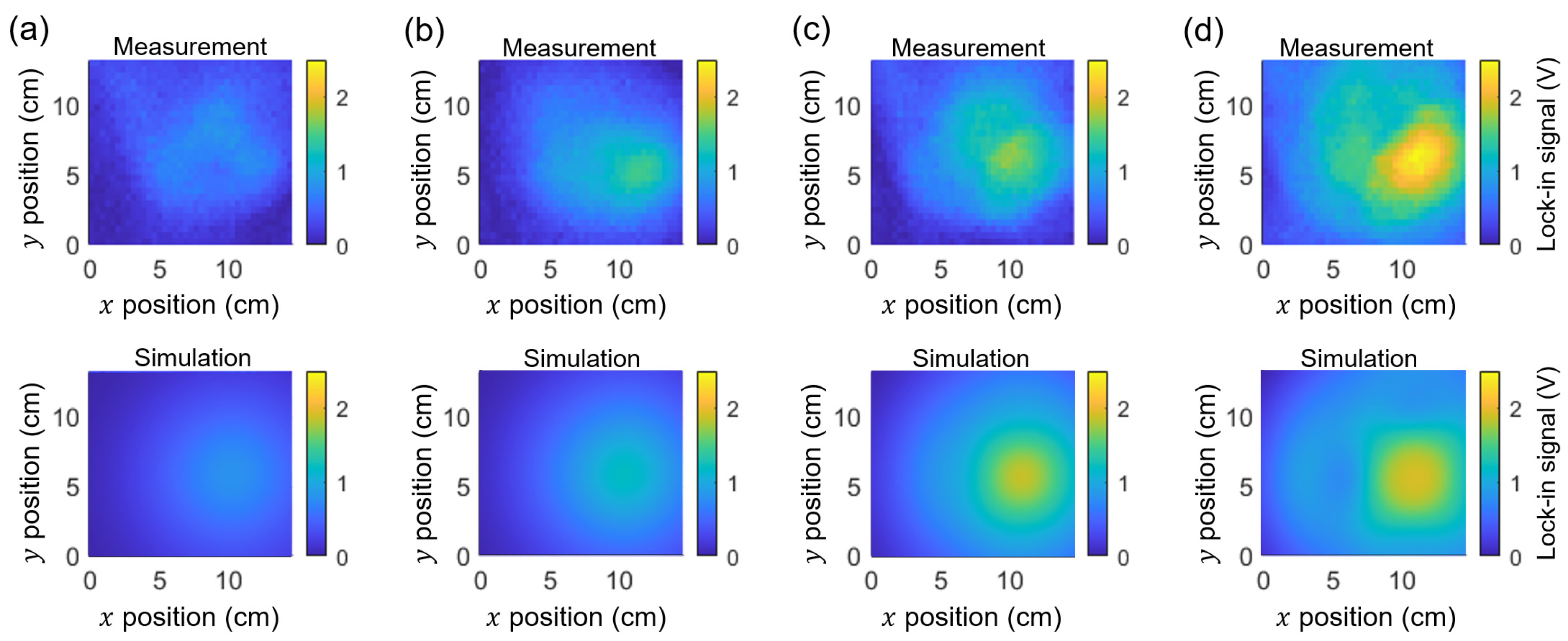
Figure 10 compares the measured and simulated lock-in images for magents of various sizes: (diameter, thickness) = (8 mm, 9 mm), (8 mm, 12 mm), (10 mm, 10 mm), and (10 mm, 15 mm). As the magnetic field increases from Fig. 10(a) to Fig. 10 (d), the measured images exhibit more complex patterns, but can be well identified by the simulation.
4. Conclusion
In this paper, we employed miniaturized NV magnetic sensors combined with a two-dimensional scanning stage to image concealed magnets in a toy diorama with millimeter-scale resolution. To expediate the overall measurement process, we utilized the lock-in detection method for the NV’s ODMR resonances. We observed that the magnetic images could be suppressed and distorted depending on the choice of fixed frequency points and the magnitude of the sample’s magnetic field. We performed magnetic simulations to analyze the evolution of the lock-in data as a function of the magnetic field and found good agreement between the measurements and simulations. A prior understanding of this evolution and subsequent image analysis is essential when using the miniaturized sensor to detect targets and extract their magnetic properties from the images. Our work offers a novel approach for using scanning miniaturized magnetometers and provides detailed analysis methods, which could be applied in military and industrial sectors to detect concealed objects and targets.
Author Contributions
W.C., C.P., D.L., J.P., and D.L. conceived and designed the experiments; W.C. and C.P. constructred sensor and scanning setup; W.C., C.P., M.L., H-Y.K., K.Y.L., S.D.L., and D.J. performed experiments, analysis, and simulations; S-H.K. and D.L. directed and supervised the project; W.C., C.P., D.L., J.P., and D.L. wrote the manuscript with contributions from all co-authors.
Funding
Research funded by Information & communication Technology Planning & Evaluation (IITP) grant (No. RS-2023-00230717), Information Technology Research Center (ITRC) support program (IITP-2024-2020-0-01606), and Creation of the Quantum Information Science R&D Ecosystem (Grant No. 2022M3H3A106307411) through the National Research Foundation of Korea (NRF) funded by the Korean government (Ministry of Science and ICT).
Institutional Review Board Statement
Not applicable.
Informed Consent Statement
Not applicable.
Data Availability Statement
Data used in this study is available upon request to the corresponding author.
Conflicts of Interest
The authors declare no conflicts of interest.
Abbreviations
The following abbreviations are used in this manuscript:
| NV | Nitrogen vacancy |
| ODMR | Optically detected magnetic resonance |
| LED | Light emitting diode |
| SQUID | Superconducting quantum interferecne device |
| PL | Photoluminescence |
| ESR | Electron spin resonance |
| PCB | Printed circuit board |
| DSRR | Double split-ring resonator |
| GRIN | Gradient-index |
| SNR | Signal-to-noise ratio |
| OPM | Optically pumped magnetometer |
| UAV | Unmanned aerial vehicles |
| OOMMF | Object oriented micromagnetic framework |
References
- Nielsen, M.A.; Chuang, I.L. Quantum Computation and Quantum Information; Cambridge university press, 2010.
- Degen, C.L.; Reinhard, F.; Cappellaro, P. Quantum Sensing. Rev. Mod. Phys. 2017, 89, 035002. [Google Scholar] [CrossRef]
- Barry, J.F.; Schloss, J.M.; Bauch, E.; Turner, M.J.; Hart, C.A.; Pham, L.M.; Walsworth, R.L. Sensitivity Optimization for NV-Diamond Magnetometry. Rev. Mod. Phys. 2020, 92, 015004. [Google Scholar] [CrossRef]
- Simmonds, M.; Fertig, W.; Giffard, R. Performance of a Resonant Input SQUID Amplifier System. IEEE Transactions on Magnetics 1979, 15, 478–481. [Google Scholar] [CrossRef]
- Casacio, C.A.; Madsen, L.S.; Terrasson, A.; Waleed, M.; Barnscheidt, K.; Hage, B.; Taylor, M.A.; Bowen, W.P. Quantum-Enhanced Nonlinear Microscopy. Nature 2021, 594, 201–206. [Google Scholar] [CrossRef] [PubMed]
- Dang, H.B.; Maloof, A.C.; Romalis, M.V. Ultrahigh Sensitivity Magnetic Field and Magnetization Measurements with an Atomic Magnetometer. Applied Physics Letters 2010, 97. [Google Scholar] [CrossRef]
- Balasubramanian, G.; Chan, I.Y.; Kolesov, R.; Al-Hmoud, M.; Tisler, J.; Shin, C.; Kim, C.; Wojcik, A.; Hemmer, P.R.; Krueger, A. Nanoscale Imaging Magnetometry with Diamond Spins under Ambient Conditions. Nature 2008, 455, 648–651. [Google Scholar] [CrossRef]
- Casola, F.; Van Der Sar, T.; Yacoby, A. Probing Condensed Matter Physics with Magnetometry Based on Nitrogen-Vacancy Centres in Diamond. Nature Reviews Materials 2018, 3, 1–13. [Google Scholar] [CrossRef]
- Lee, M.; Jang, S.; Jung, W.; Lee, Y.; Taniguchi, T.; Watanabe, K.; Kim, H.-R.; Park, H.-G.; Lee, G.-H.; Lee, D. Mapping Current Profiles of Point-Contacted Graphene Devices Using Single-Spin Scanning Magnetometer. Applied Physics Letters 2021, 118. [Google Scholar] [CrossRef]
- Webb, J.L.; Clement, J.D.; Troise, L.; Ahmadi, S.; Johansen, G.J.; Huck, A.; Andersen, U.L. Nanotesla Sensitivity Magnetic Field Sensing Using a Compact Diamond Nitrogen-Vacancy Magnetometer. Applied Physics Letters 2019, 114. [Google Scholar] [CrossRef]
- Zheng, D.; Ma, Z.; Guo, W.; Niu, L.; Wang, J.; Chai, X.; Li, Y.; Sugawara, Y.; Yu, C.; Shi, Y. A Hand-Held Magnetometer Based on an Ensemble of Nitrogen-Vacancy Centers in Diamond. Journal of Physics D: Applied Physics 2020, 53, 155004. [Google Scholar] [CrossRef]
- Patel, R.L.; Zhou, L.Q.; Frangeskou, A.C.; Stimpson, G.A.; Breeze, B.G.; Nikitin, A.; Dale, M.W.; Nichols, E.C.; Thornley, W.; Green, B.L.; et al. Subnanotesla Magnetometry with a Fiber-Coupled Diamond Sensor. Phys. Rev. Applied 2020, 14, 044058. [Google Scholar] [CrossRef]
- Kim, D.; Ibrahim, M.I.; Foy, C.; Trusheim, M.E.; Han, R.; Englund, D.R. A CMOS-Integrated Quantum Sensor Based on Nitrogen–Vacancy Centres. Nature Electronics 2019, 2, 284–289. [Google Scholar] [CrossRef]
- Aslam, N.; Zhou, H.; Urbach, E.K.; Turner, M.J.; Walsworth, R.L.; Lukin, M.D.; Park, H. Quantum Sensors for Biomedical Applications. Nature Reviews Physics 2023, 5, 157–169. [Google Scholar] [CrossRef] [PubMed]
- Pelliccione, M.; Jenkins, A.; Ovartchaiyapong, P.; Reetz, C.; Emmanouilidou, E.; Ni, N.; Bleszynski Jayich, A.C. Scanned Probe Imaging of Nanoscale Magnetism at Cryogenic Temperatures with a Single-Spin Quantum Sensor. Nature nanotechnology 2016, 11, 700–705. [Google Scholar] [CrossRef] [PubMed]
- Maletinsky, P.; Hong, S.; Grinolds, M.S.; Hausmann, B.; Lukin, M.D.; Walsworth, R.L.; Loncar, M.; Yacoby, A. A Robust Scanning Diamond Sensor for Nanoscale Imaging with Single Nitrogen-Vacancy Centres. Nature nanotechnology 2012, 7, 320–324. [Google Scholar] [CrossRef]
- Thiel, L.; Wang, Z.; Tschudin, M.A.; Rohner, D.; Gutiérrez-Lezama, I.; Ubrig, N.; Gibertini, M.; Giannini, E.; Morpurgo, A.F.; Maletinsky, P. Probing Magnetism in 2D Materials at the Nanoscale with Single-Spin Microscopy. Science 2019, 364, 973–976. [Google Scholar] [CrossRef]
- Gross, I.; Akhtar, W.; Garcia, V.; Martínez, L.J.; Chouaieb, S.; Garcia, K.; Carrétéro, C.; Barthélémy, A.; Appel, P.; Maletinsky, P. Real-Space Imaging of Non-Collinear Antiferromagnetic Order with a Single-Spin Magnetometer. Nature 2017, 549, 252–256. [Google Scholar] [CrossRef]
- Ku, M.J.; Zhou, T.X.; Li, Q.; Shin, Y.J.; Shi, J.K.; Burch, C.; Anderson, L.E.; Pierce, A.T.; Xie, Y.; Hamo, A. Imaging Viscous Flow of the Dirac Fluid in Graphene. Nature 2020, 583, 537–541. [Google Scholar] [CrossRef] [PubMed]
- Chen, S.; Park, S.; Vool, U.; Maksimovic, N.; Broadway, D.A.; Flaks, M.; Zhou, T.X.; Maletinsky, P.; Stern, A.; Halperin, B.I. Current Induced Hidden States in Josephson Junctions. Nature Communications 2024, 15, 8059. [Google Scholar] [CrossRef]
- Le Sage, D.; Arai, K.; Glenn, D.R.; DeVience, S.J.; Pham, L.M.; Rahn-Lee, L.; Lukin, M.D.; Yacoby, A.; Komeili, A.; Walsworth, R.L. Optical Magnetic Imaging of Living Cells. Nature 2013, 496, 486–489. [Google Scholar] [CrossRef]
- Yoon, J.; Moon, J.H.; Chung, J.; Kim, Y.J.; Kim, K.; Kang, H.S.; Jeon, Y.S.; Oh, E.; Lee, S.H.; Han, K.; et al. Exploring the Magnetic Properties of Individual Barcode Nanowires Using Wide-Field Diamond Microscopy. Small 2023, 19, 2304129. [Google Scholar] [CrossRef]
- Chen, S.; Li, W.; Zheng, X.; Yu, P.; Wang, P.; Sun, Z.; Xu, Y.; Jiao, D.; Ye, X.; Cai, M.; et al. Immunomagnetic Microscopy of Tumor Tissues Using Quantum Sensors in Diamond. Proc. Natl. Acad. Sci. U.S.A. 2022, 119, e2118876119. [Google Scholar] [CrossRef]
- Barry, J.F.; Turner, M.J.; Schloss, J.M.; Glenn, D.R.; Song, Y.; Lukin, M.D.; Park, H.; Walsworth, R.L. Optical Magnetic Detection of Single-Neuron Action Potentials Using Quantum Defects in Diamond. Proc. Natl. Acad. Sci. U.S.A. 2016, 113, 14133–14138. [Google Scholar] [CrossRef] [PubMed]
- Glenn, D.R.; Fu, R.R.; Kehayias, P.; Le Sage, D.; Lima, E.A.; Weiss, B.P.; Walsworth, R.L. Micrometer-scale Magnetic Imaging of Geological Samples Using a Quantum Diamond Microscope. Geochem Geophys Geosyst 2017, 18, 3254–3267. [Google Scholar] [CrossRef]
- Nowodzinski, A.; Chipaux, M.; Toraille, L.; Jacques, V.; Roch, J.-F.; Debuisschert, T. Nitrogen-Vacancy Centers in Diamond for Current Imaging at the Redistributive Layer Level of Integrated Circuits. Microelectronics Reliability 2015, 55, 1549–1553. [Google Scholar] [CrossRef]
- Gruber, A.; Dräbenstedt, A.; Tietz, C.; Fleury, L.; Wrachtrup, J.; Borczyskowski, C.V. Scanning Confocal Optical Microscopy and Magnetic Resonance on Single Defect Centers. Science 1997, 276, 2012–2014. [Google Scholar] [CrossRef]
- Bayat, K.; Choy, J.; Farrokh Baroughi, M.; Meesala, S.; Loncar, M. Efficient, Uniform, and Large Area Microwave Magnetic Coupling to NV Centers in Diamond Using Double Split-Ring Resonators. Nano Lett. 2014, 14, 1208–1213. [Google Scholar] [CrossRef] [PubMed]
- Yang, Y.; Wu, Q.; Wang, Y.; Chen, W.; Yu, Z.; Yang, X.; Fan, J.-W.; Chen, B. Tunable Double Split-Ring Resonator for Quantum Sensing Using Nitrogen-Vacancy Centers in Diamond. Opt. Continuum, OPTCON 2023, 2, 1426–1435. [Google Scholar] [CrossRef]
- Dassault Systèmes. (2023). CST Studio Suite (버전 2023). Retrieved from https://www.3ds.com/products-services/simulia/products/cst-studio-suite/.
- Lee, K.W.; Lee, D.; Ovartchaiyapong, P.; Minguzzi, J.; Maze, J.R.; Bleszynski Jayich, A.C. Strain Coupling of a Mechanical Resonator to a Single Quantum Emitter in Diamond. Phys. Rev. Applied 2016, 6, 034005. [Google Scholar] [CrossRef]
- Lee, D.; Lee, K.W.; Cady, J.V.; Ovartchaiyapong, P.; Jayich, A.C.B. Topical Review: Spins and Mechanics in Diamond. Journal of Optics 2017, 19, 033001. [Google Scholar] [CrossRef]
- Dréau, A.; Lesik, M.; Rondin, L.; Spinicelli, P.; Arcizet, O.; Roch, J.-F.; Jacques, V. Avoiding Power Broadening in Optically Detected Magnetic Resonance of Single NV Defects for Enhanced Dc Magnetic Field Sensitivity. Phys. Rev. B 2011, 84, 195204. [Google Scholar] [CrossRef]
- Stürner, F.M.; Brenneis, A.; Kassel, J.; Wostradowski, U.; Rölver, R.; Fuchs, T.; Nakamura, K.; Sumiya, H.; Onoda, S.; Isoya, J. Compact Integrated Magnetometer Based on Nitrogen-Vacancy Centres in Diamond. Diamond and Related Materials 2019, 93, 59–65. [Google Scholar] [CrossRef]
- Bernardi, E.; Moreva, E.; Traina, P.; Petrini, G.; Tchernij, S.D.; Forneris, J.; Pastuović, Ž.; Degiovanni, I.P.; Olivero, P.; Genovese, M. A Biocompatible Technique for Magnetic Field Sensing at (Sub) Cellular Scale Using Nitrogen-Vacancy Centers. EPJ Quantum Technology 2020, 7, 13. [Google Scholar] [CrossRef]
- Mu, Y.; Zhang, X.; Xie, W.; Zheng, Y. Automatic Detection of Near-Surface Targets for Unmanned Aerial Vehicle (UAV) Magnetic Survey. Remote Sensing 2020, 12, 452. [Google Scholar] [CrossRef]
- Accomando, F.; Florio, G. Drone-Borne Magnetic Gradiometry in Archaeological Applications. Sensors 2024, 24, 4270. [Google Scholar] [CrossRef]
- Application of a Drone Magnetometer System to Military Mine Detection in the Demilitarized Zone. Available online: https://www.mdpi.com/1424-8220/21/9/3175 (accessed on 9 December 2024).
- Zheng, Y.; Li, S.; Xing, K.; Zhang, X. Unmanned Aerial Vehicles for Magnetic Surveys: A Review on Platform Selection and Interference Suppression. Drones 2021, 5, 93. [Google Scholar] [CrossRef]
- Gailler, L.; Labazuy, P.; Régis, E.; Bontemps, M.; Souriot, T.; Bacques, G.; Carton, B. Validation of a New UAV Magnetic Prospecting Tool for Volcano Monitoring and Geohazard Assessment. Remote Sensing 2021, 13, 894. [Google Scholar] [CrossRef]
- Donahue, M. J., & Porter, D. G. (1999). OOMMF User's Guide, Version 1.0. Interagency Report NISTIR 6376, National Institute of Standards and Technology, Gaithersburg, MD. Retrieved from https://math.nist.gov/oommf/doc/userguide20a0/userguide.pdf.
- Kuwahata, A.; Kitaizumi, T.; Saichi, K.; Sato, T.; Igarashi, R.; Ohshima, T.; Masuyama, Y.; Iwasaki, T.; Hatano, M.; Jelezko, F. Magnetometer with Nitrogen-Vacancy Center in a Bulk Diamond for Detecting Magnetic Nanoparticles in Biomedical Applications. Scientific reports 2020, 10, 2483. [Google Scholar] [CrossRef]
- Wang, X.; Zheng, D.; Wang, X.; Liu, X.; Wang, Q.; Zhao, J.; Guo, H.; Qin, L.; Tang, J.; Ma, Z.; et al. Portable Diamond NV Magnetometer Head Integrated With 520 Nm Diode Laser. IEEE Sensors Journal 2022, 22, 5580–5587. [Google Scholar] [CrossRef]
- Xie, F.; Liu, Q.; Hu, Y.; Li, L.; Chen, Z.; Zhang, J.; Zhang, Y.; Zhang, Y.; Wang, Y.; Cheng, J. A Microfabricated Diamond Quantum Magnetometer with Picotesla Scale Sensitivity. In Proceedings of the 2023 IEEE 36th International Conference on Micro Electro Mechanical Systems (MEMS); IEEE, 2023; pp. 157–160.
- Stürner, F.M.; Brenneis, A.; Buck, T.; Kassel, J.; Rölver, R.; Fuchs, T.; Savitsky, A.; Suter, D.; Grimmel, J.; Hengesbach, S.; et al. Integrated and Portable Magnetometer Based on Nitrogen-Vacancy Ensembles in Diamond. Adv Quantum Tech 2021, 4, 2000111. [Google Scholar] [CrossRef]
Figure 1.
Schematics of (a) single spin scanning magnetometry, (b) wide-field diamond microscopy, and (c) scanning miniaturized magnetometry.
Figure 1.
Schematics of (a) single spin scanning magnetometry, (b) wide-field diamond microscopy, and (c) scanning miniaturized magnetometry.
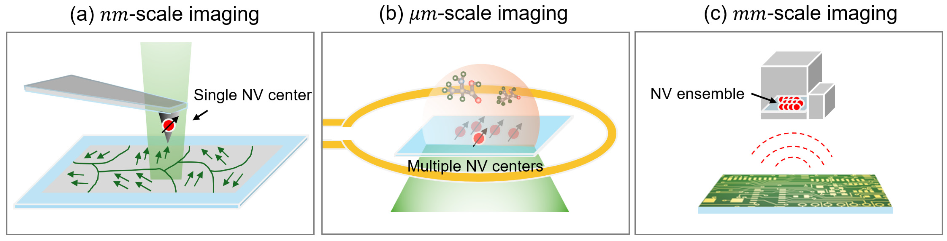
Figure 2.
(a) A schematic of an NV center within a diamond lattice, showing four possible crystal axes of the NV centers. (b) A diagram illustrating the NV’s ground-state energy levels. The spin states of and are separated by 2.87 GHz at room temperature and the degenerated states can be split by an external magnetic field along the NV’s axis, . The NV’s photoluminescence signal is smaller for compared to , as indicated by the relative widths of the red arrows. (c) ODMR spectra for a single NV center (upper plot) and ensemble NV centers (lower plot). In the ensemble spectrum, four pairs of spin resonances appear when exposed to an external magnetic field.

Figure 3.
Pictures of miniaturized sensors based on two light sources: (a) a LED and (b) a fiber-coupled external laser. A DSRR is employed to efficiently deliver microwave fields from an external microwave generator to the NV centers. (c) A schematic of the sensor setups. Either the LED or the fiber-coupled laser provides excitation light at λ = 532 nm. The NV’s photoluminescence is collected by a photodetector after a GRIN lens, a dichroic mirrors, pairs of lenses, and an optical filter. The lock-in detection technique is used to enhance the SNR of photoluminescence signal.

Figure 4.
(a) DSRR return loss, S11, simulation (blue solid line) and measurement (orange solid line). The measured quality factor Q is 395. The inset illustrates the simulated normal component of the microwave field around 2.8 GHz, with the white rectangle indicating a the copper plate to adjust the DSRR’s resonance frequency. Scale bar = 5 mm. (b) The measured S11 after matching the resonance frequencies between the NV center and the microwave resonator. The quality factor Q is reduced to 160 due to the insertion of the copper.
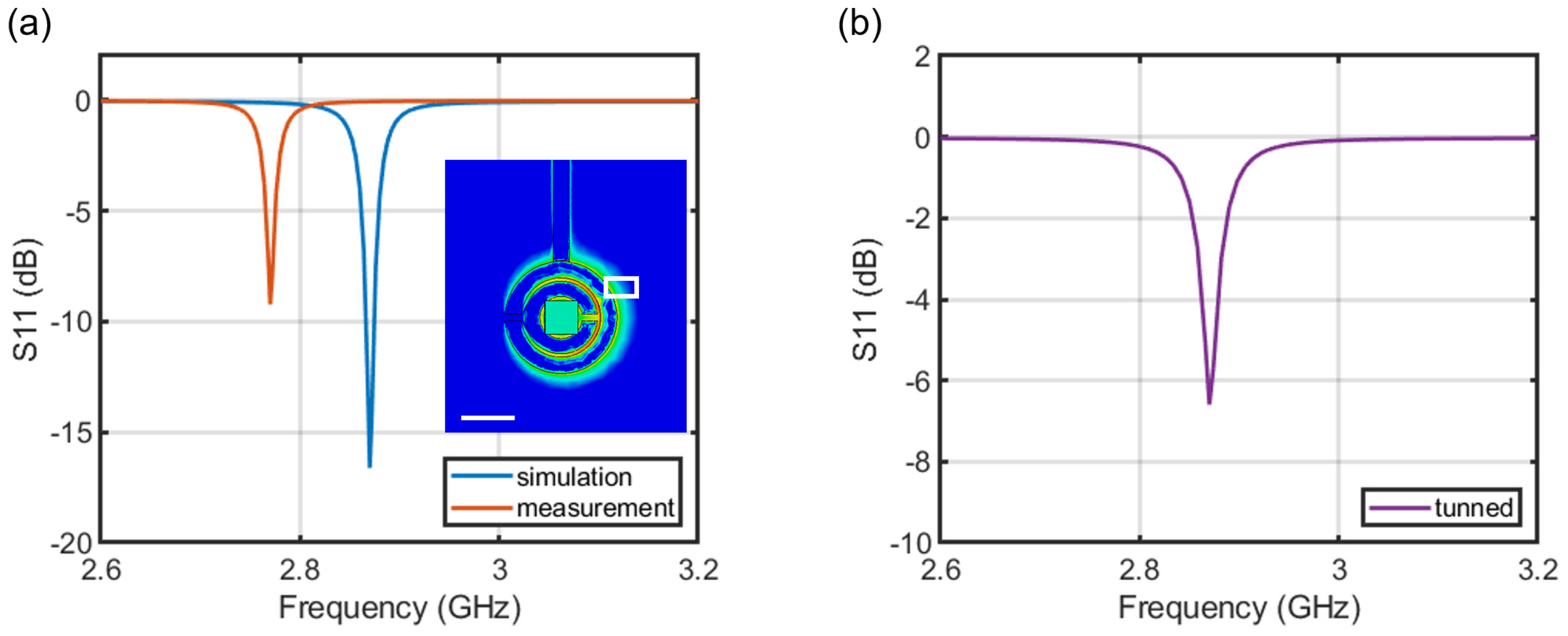
Figure 5.
(a) ODMR spectrum measured by the sensor in Fig. 3(a). (b) Derivative of the ODMR data in (a). (c) Lock-in result of the same measurement in (a). (d) Contrast, C, and linewidth, Δf, of the ODMR resonance as a function of the microwave power, PMW. The inset plots C/Δf as a function of PMW. (e) Calculated sensitivity, , from the lock-in data as a function of PMW.
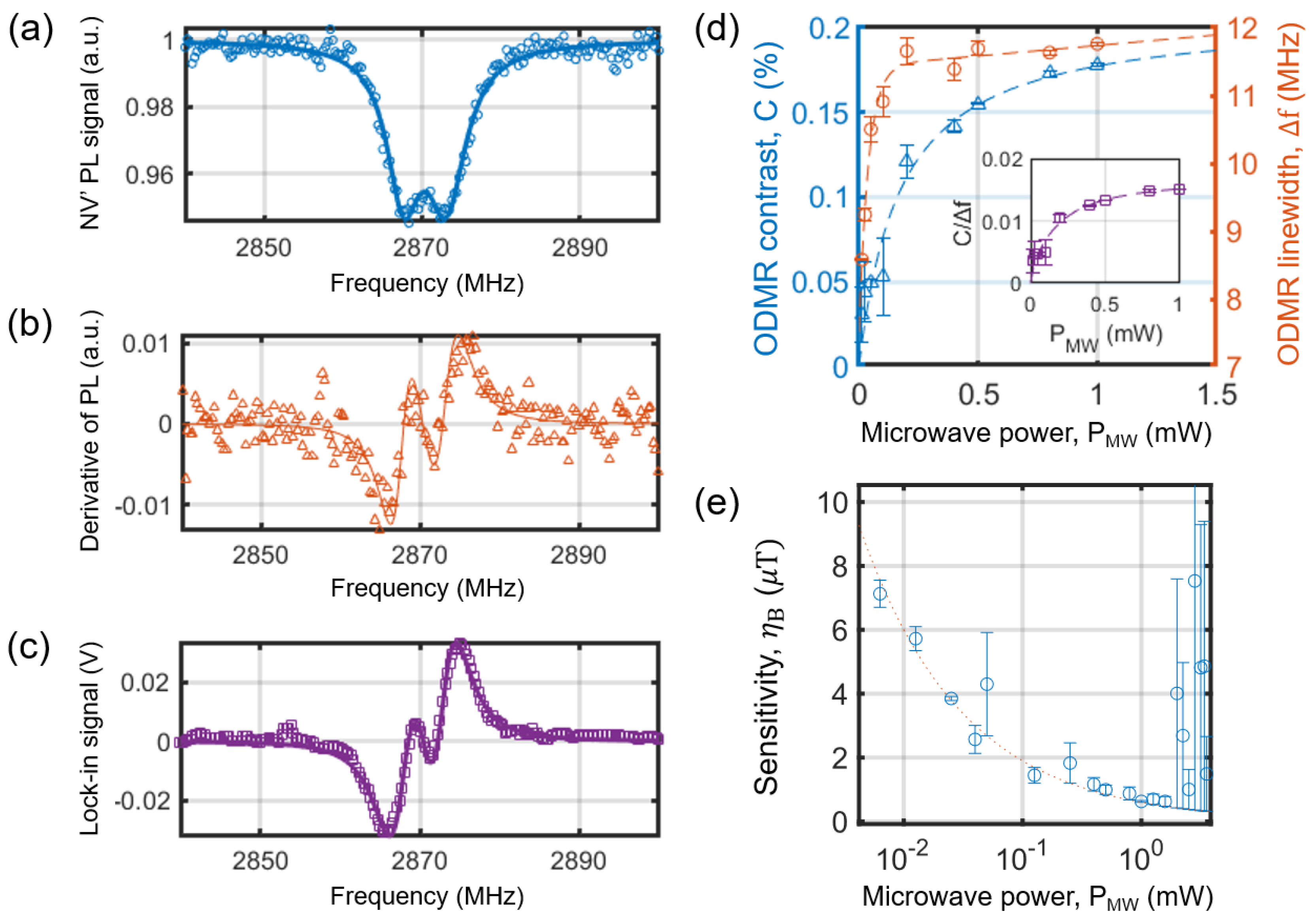
Figure 6.
(a) Scanning miniaturized magnetometer setup. The miniaturized sensor, as shown in Fig. 3(a) and (b), is mounted on a 2D mobile stage that is controlled by two stepper motors. Diorama and concealed magnets are used to emulate landmines buried underground. (b) The measured and simulated magnetic field maps of three hidden Nd magnets. The magnetic image clearly reveals the locations of the hidden objects.
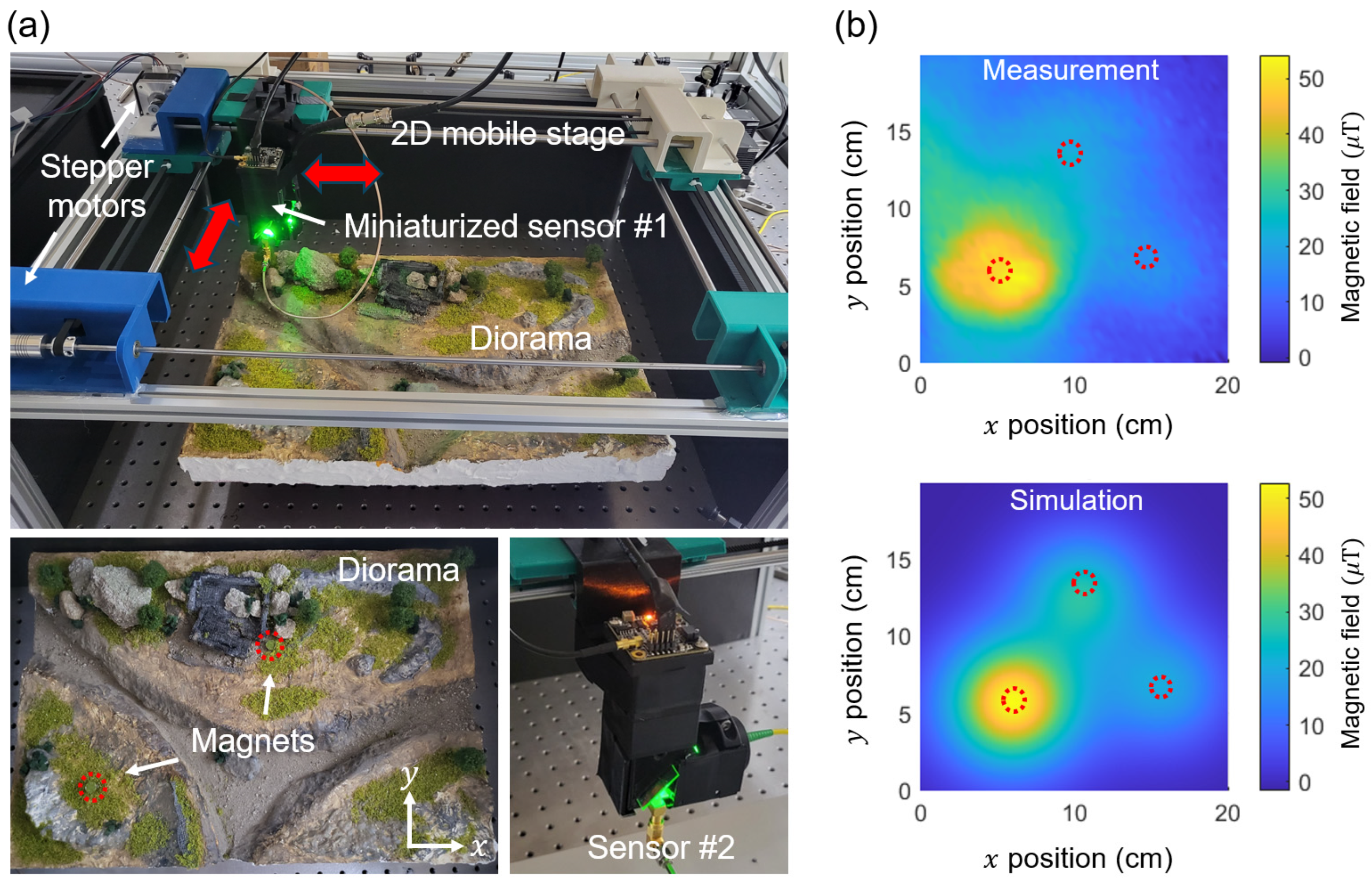
Figure 7.
(a) An example of the lock-in measurement. The frequency point marked as ① corresponds to the point where the lock-in signal is at its maximum. The right panel shows a zoom-in of the dashed rectangle in the left panel. The frequency point marked as ② represents the middle of the frequency range, where the lock-in signal varies linearly. (b) Normalized lock-in signal as a function of the magnetic field along the NV axis, , calculated at the fixed frequency points ① and ②. The right panel is a zoom-in of the region I from the left panel.
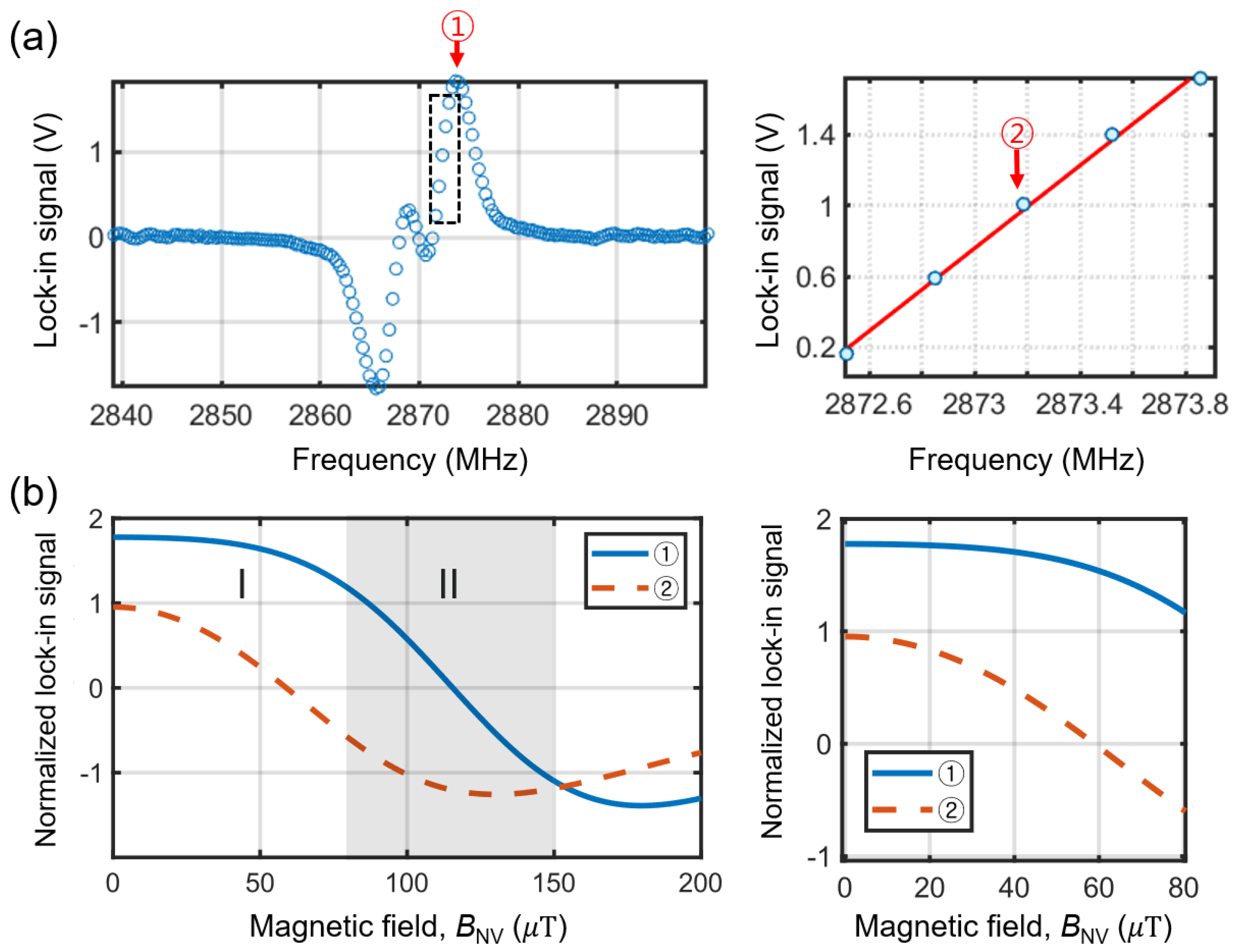
Figure 8.
Magnetic images of Nd disk magnets with dimensions (diameter, thickness) = (8 mm, 3mm) for (a) and (5 mm, 3 mm) for (b), measured at the fixed frequency points , ① and ②. The lower panels show the line-cut profiles along the dahsed lines in the upper images. The lock-in signals measured at ① are ~ 77% (a) and ~63% (b) of the signals measured at ②.
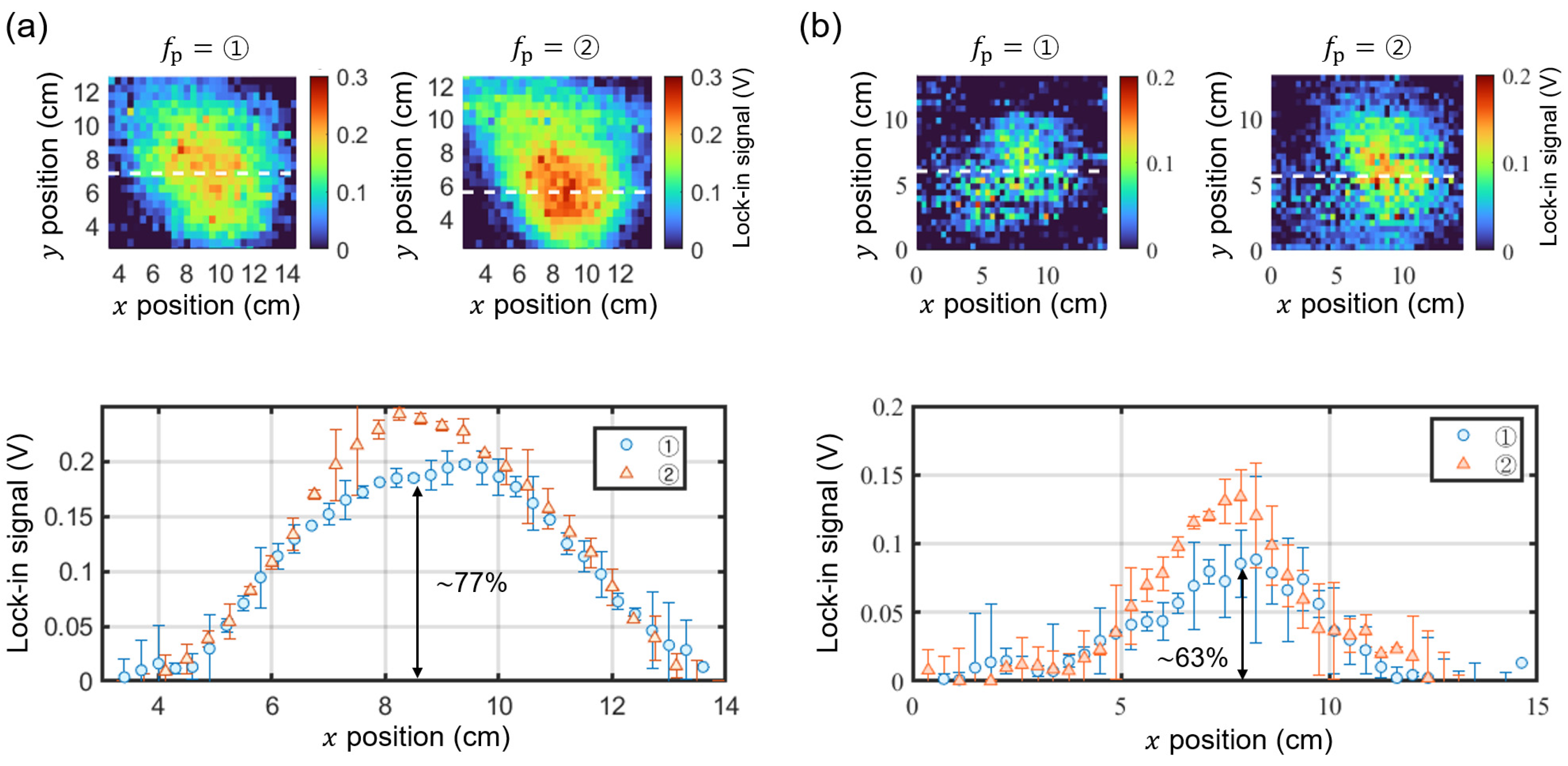
Figure 9.
(a) A schematic of relative angle between the NV centers in a miniaturized sensor and a magnet. and denote the tilt angles along the x- and y-axis. (b) Calculated magnetic field from the magnet at z = 10, . Dimension of the magnet is (diameter, thickness) = (10 mm, 15 mm). (c) Absolute magnetic field projected onto the NV axis, . All NV axes are considered. (d) Magnetic image considering the relative tilt angles between the sensor and magnet, . The tilt angles used for the simulation are and . (e) Calculated lock-in signal incorporating the Zeeman shift due to .
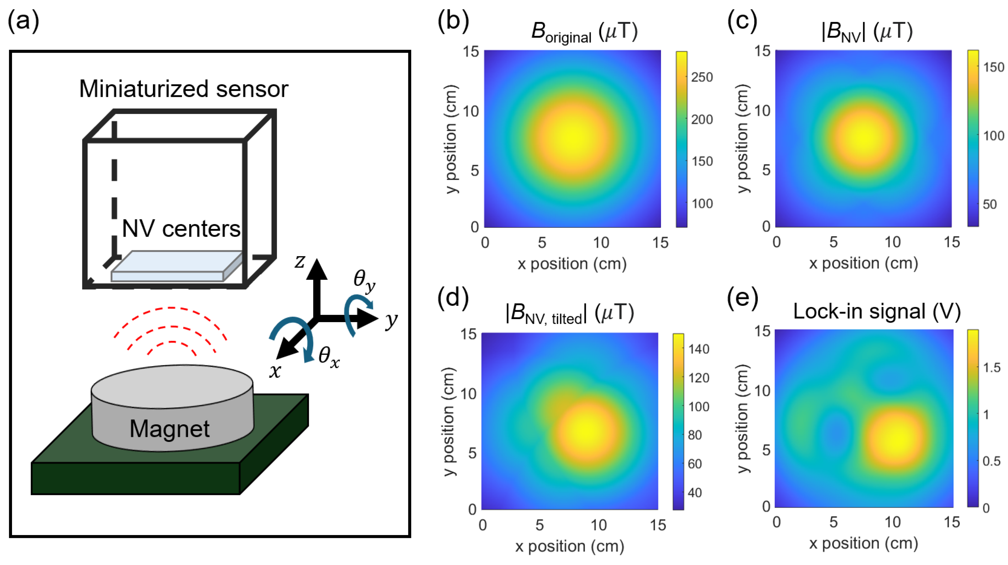
Figure 10.
Measured and simulated lock-in images for magnets with dimensions (diameter, thickness) = (8 mm, 9 mm) (a), (8 mm, 12 mm) (b), (10 mm, 10 mm) (c), and (10 mm, 15 mm) (d). The measured images show stronger distortion, with more pronounced nodal lines. The simulations successfully capture the patterns observed in the measured images.
Disclaimer/Publisher’s Note: The statements, opinions and data contained in all publications are solely those of the individual author(s) and contributor(s) and not of MDPI and/or the editor(s). MDPI and/or the editor(s) disclaim responsibility for any injury to people or property resulting from any ideas, methods, instructions or products referred to in the content. |
© 2024 by the authors. Licensee MDPI, Basel, Switzerland. This article is an open access article distributed under the terms and conditions of the Creative Commons Attribution (CC BY) license (http://creativecommons.org/licenses/by/4.0/).
Copyright: This open access article is published under a Creative Commons CC BY 4.0 license, which permit the free download, distribution, and reuse, provided that the author and preprint are cited in any reuse.


