
Submitted:
07 December 2024
Posted:
09 December 2024
You are already at the latest version
Abstract
Rapid thermal annealing (RTA) has been widely used in the process of semiconductor devices. However, the rise time of RTA is limited by millisecond (ms) that is not suitable for advanced nanometre scale electron devices. Using sub-energy bandgap (EG) 532 nm ultra-fast 15 nanosecond (ns) pulsed laser annealing, the record highest high dielectric constant (high-κ) of 67.8 and capacitance density of 75 fF/μm2 at -0.2 V were obtained in Ni/ZrO2/TiN capacitors According to the heat source and diffusion equations, the surface temperature of TiN can be as high as 870 °C at a laser energy density of 16.2 J/cm2, which in turn anneals the ZrO2 material. The record-breaking data are achieved by a new annealing method- the surface plasma effect generated on TiN metal. This is because the 2.3 eV (532 nm) pulsed laser energy is far below the 5.0~5.8 eV energy bandgap (EG) of ZrO2, which cannot be absorbed by the ZrO2 dielectric. From X-ray diffraction analysis, the large κ value and capacitance density are attributed the crystallinity of cubic phase ZrO2 that is improved with laser annealing and in turn improves the capacitance density. This technology is crucial for monolithic three-dimensional devices integration on the backend of advanced integrated circuit.
Keywords:
High-κ
; laser anneal
; Metal insulator metal
; TiN
; ZrO2
1. Introduction
In the past decades, thermal annealing has progressed toward shorter cycles with higher temperatures. Crystallization by furnace requires high-temperature heat treatment, which causes long diffusion length and fails the small channel electron devices. To improve the impurity diffusion, Rapid Thermal Annealing (RTA) was used to replace the furnace annealing. Current spike RTA has a temperature ramp up at 400 °C/s to decrease the thermal diffusion effect. One major limitation of spike RTA is that the irradiation energy must be larger than the energy bandgap (EG) of the materials. However, the UV-visible light irradiation energy of RTA is lower than the wide EG dielectrics in the backend of Integrated Circuits (ICs). Although indirect heating is available by Si substrate, the annealing effect on backend devices is insufficient. Besides, the maximum temperature for backend IC process is limited to 400 °C to prevent damage to frontend CMOS transistors.
In this study, we propose a new annealing method to improve the device quality for backend devices on isolation oxide. To further improve the impurity diffusion, a nanosecond (ns) pulsed laser is used. The proposed idea was verified by the large enhancement of 75 fF/μm2 capacitance density and high dielectric constant (high-κ) of 67.8 by using 15 ns laser annealing, in the ZrO2 metal-insulator-metal (MIM) device. These are the highest κ value and capacitance density reported in literature [1,2,3]. It is important to notice that the laser light energy significantly lower than energy bandgap of material, where the mechanism is due to the surface plasma effect [4] to create high-temperature on metal surface and heat up the ZrO2 dielectric. The temperature profile under various laser annealing density is calculated using Matrix Laboratory (MATLAB). The peak temperature at TiN metal surface can be as high as 870°C, which can anneal above ZrO2 dielectric efficiently. On the other hand, the temperature is largely decreased below the 400°C within a TiN thickness of 30 nm, which meets the requirement with little effect on frontend CMOS transistors. This technology can improve the devices performance for Monolithic Three-Dimensional (M3D) integration on the backend of advanced Integrated Circuit (IC). Such M3D integration is crucible to improve the circuit speed and switching power consumption beyond the most advanced microprocessors [5,6,7].
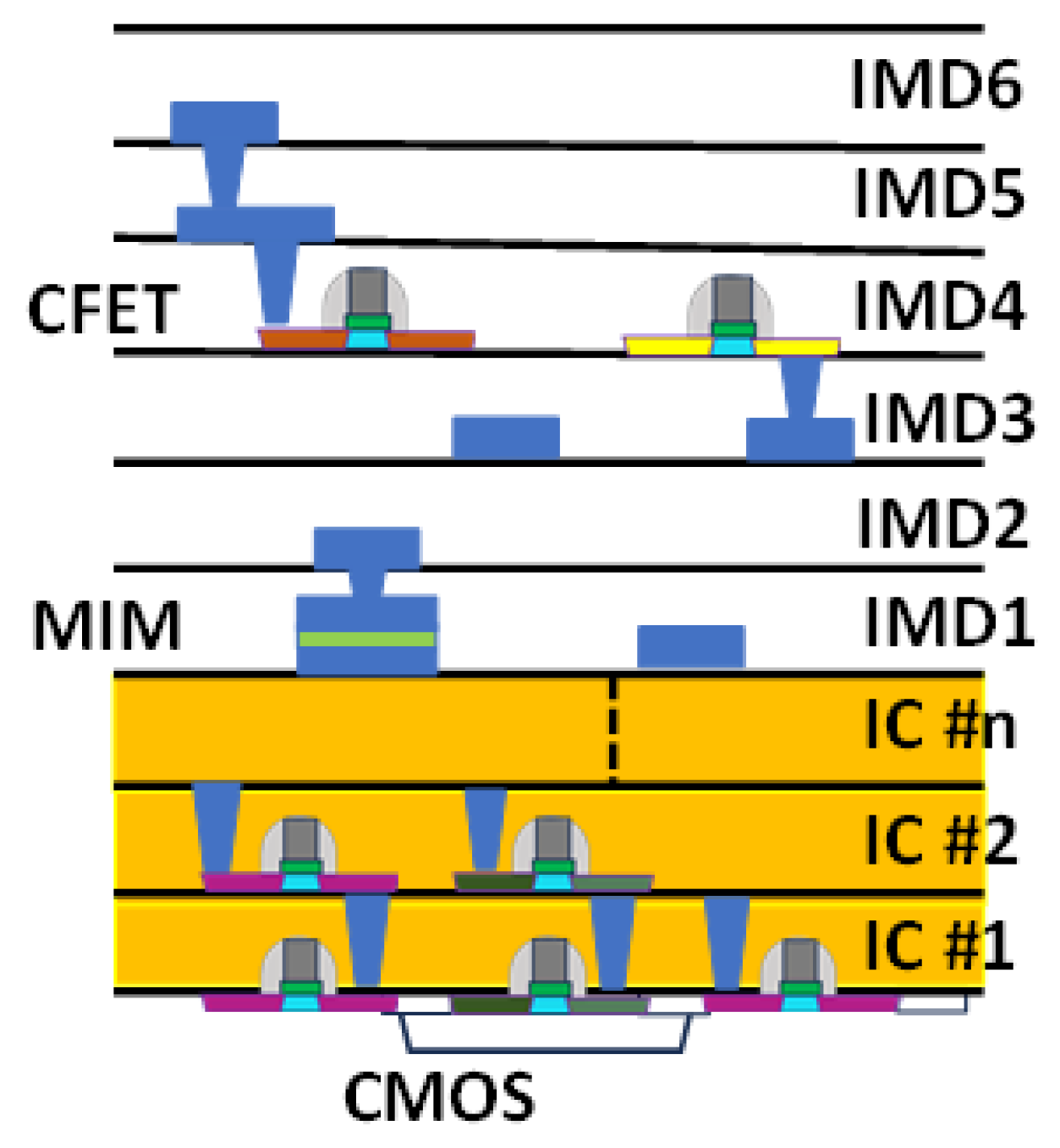
Figure 1.
Monolithic Three-Dimensional (M3D) Integrated Circuit (IC).
2. Materials and Methods
A 50 nm TiN was first deposited and patterned as the bottom electrode for metal insulator metal (MIM) capacitor. Followed by NH3+ plasma treatment conditions under 2000 W (60 s and 120 s), 2400 W (60 s) and 2800 W (60 s) respectively to prevent capacitance-equivalent-thickness (CET) degradation by forming interfacial TiON during post-deposition annealing (PDA). Next, an 8 nm ZrO2 layer was deposited via atomic layer deposition (ALD), and O2-PDA at 400°C for 30 min to improve its dielectric quality. The ALD has a self-assembly mechanism with atomic layer-by-layer growth and precise thickness control. A HIPPO mid power Q-switched laser 532 nm with 5.4 J/cm2, 16.2 J/cm2 and 21.6 J/cm2, was applied. Finally, a 50 nm Ni top electrode was deposited. The devices were characterized by capacitance density-voltage (C–V) and current density-voltage (J–V) measurements. Laser annealed (LA) samples was calculated using MATLAB to analyse temperature profile effectively. X-ray diffraction (XRD), Transmission electron microscope (TEM) and atomic force microscope (AFM) are used to understand the material quality and improvements.
3. Results
The heat diffusion equation governing the temperature evolution in both the TiN and ZrO2 layers is given by:
Where α is the thermal diffusivity, ∇2T is the Laplacian of the temperature (describing the spatial derivatives of temperature in both radial and axial directions), k is thermal conductivity, ρ is material density, cp is specific heat capacity, Q is the heat source term (which is zero for ZrO2, but non-zero in TiN due to laser absorption). The heat is in a Gaussian profile in the radial direction because the laser beam typically has a Gaussian intensity profile. In the radial direction, the heat source term is expressed as:
Where ATiN is absorbance of TiN layer, TZrO2 is transmittance of ZrO2, E is laser energy, A is spot size, t is laser irradiation time and σ is related to the focal radius, representing the width of the Gaussian beam profile, n1 is the refractive index of ZrO2 and n2 is the refractive index of air. The ZrO2 dielectric exhibited negligible absorption of laser energy, as its bandgap (5 to 5.8 eV) [8,9] significantly surpasses the photon energy of 2.33 eV. The increase in temperature can be attributed to the heat converted from the photon energy absorbed by TiN layer.
Figure 2 (a)-(c) present the simulation results of the temperature increase when laser irradiation with an energy density fluence of 5.4, 16.2 and 21.6 J/cm2. TiN, a good plasmonic media is used as a metal layer to enhance the absorption of the irradiated pulse laser and diffuse the heat to ZrO2 insulator layer above it [10,11]. The calculation displayed that the average temperature increases to 350 °C, 870 °C and 1450 °C at TiN surface and as heat diffuses, the temperature at ZrO2 is 320 °C, 800 °C and 1300 °C, as the laser annealed energy density fluences are 5.4 J/cm2, 16.2 J/cm2 and 21.6 J/cm2, respectively.
Further, Lu et al. reported that ammonia (NH3) plasma pre-treatment is crucial before the deposition of high-κ materials, as it significantly enhances interface properties [12]. Edwards et al. reported that NH3 plasma treatment prior to SiN deposition significantly improves the degradation characteristics of AlGaN–GaN high-electron-mobility transistor (HEMTs) by reducing current collapse and eliminating gate lag after extended direct current bias [13]. This process strengthens bonds, making the structure more resistant to hot electron damage and passivating defects caused by it.
Figure 3 (a)-(d) shows the C–V characteristics of Ni/ZrO2/TiN MIM capacitors before and after laser annealing under NH3+ plasma treatment conditions at 2000 W (60 s and 120 s), 2400 W (60 s) and 2800 W (60 s) respectively. The merits of using Ni electrode are the high work-function and reactive-ion-etching-friendly process [14]. For a 532 nm laser annealing with 2400 W 60s NH3+ plasma treatment in Figure 3 (c), the capacitance density increases monotonically with increasing laser-power that is 51.9 fF/um2 for 5.4 J/cm2 and 75 fF/um2 for 16.2 J/cm2 much better than the control devices before laser annealing, with a capacitance density of 41.7 fF/um2 at -0.2 V. Therefore, the 2400 W 60s NH3+ surface treatment can make better formation and density of nitridation layer. Such nitridation layer can effectively prevent the ZrO2 and TiN reaction at high temperature to form TiON. Under this condition, the plasma treatment significantly improves the TiNx surface for laser annealing. Other conditions, such as lower power (2000 W) or excessive power (2800 W), did not reach such high capacitance density due to either insufficient or excessive modification of the TiNx surface. Prolonged treatment times are less effective than the increased NH3+ plasma density. Thus, the 2400 W 60s NH3+ plasma condition represents an optimal balance on TiN surface nitridation, resulting in the best capacitance performance. Further when ZrO2/TiN is laser annealed at 532 nm using 21.6 J/cm2 energy density, it raises the temperature at TiN surface to 1450 °C and heat diffusion to ZrO2 cause the temperature to raise to 1300 °C.
Figure 4 highlights the J–V plot of Ni/ZrO2/TiN capacitor before and after laser annealing at 532 nm 16.2 J/cm2. The leakage current increases slightly by 2.67 × 10⁻⁸ A/cm2 at -0.2 V than the control devices before laser annealing, with leakage current of 2.17 × 10⁻⁸ A/cm2 at -0.2 V.
Figure 5 (a) and (b) shows the C-V and (b) J-V analysis for Ni/ZrO2/TiN MIM capacitors at higher 21.6 J/cm2 laser annealing. No capacitance can be measured and the Ni/ZrO2/TiN MIM device behaves like a small resistor. As shown in Figure 2(c), the temperature at TiN surface can raise to 1450 °C and heat diffusion to ZrO2 cause the temperature to raise to 1300 °C. The laser energy is large enough and can cause thermal stress by local temperature rise exceeding the fracture strength of the film, the film will be wrinkled, cracked or even shed leading to failure of device [15]. Although these temperatures are still less than the melting temperature of ZrO2 and TiN, such high temperature may cause ZrO2 and TiN reaction, bond breaking, free Zr and Ti metals and shorting the capacitor.
The slight increase in leakage current after laser annealing is attributed to larger grain size, as seen in XRD (Figure 6). The grain size of the ZrO2 can be calculated by using Scherrer formula as
where D is the grain size, λ is the X-ray wavelength, k =0.9 is a dimensionless shape factor, β is the line broadening at half the maximum intensity (FWHM), and θ is the Bragg angle. The calculated grain sizes of ZrO2, before and after laser annealing at 532 nm, 16.2 J/cm2 is 6.85 nm and 8.21 nm respectively. This is similar to findings in TiO2 MIM capacitors [16]. The annealing enhances ZrO2 crystallinity, particularly in the high-κ cubic phase, evident from stronger XRD peaks. This improved crystallinity explains the higher capacitance density.
The TEM analysis is used to study the laser annealing condition. Figure 7 (a) and (b) further shows the cross-sectional TEM image of Al/ZrO2/TiN structures before and after laser annealing. Clear better crystallization of ZrO2 is observed after laser annealing, which is consistent with the XRD results. In the TEM image, the relatively rough top interface is Al rather than Ni. The samples analysed by TEM cannot contain magnetic substances such as iron/cobalt/nickel and other materials.
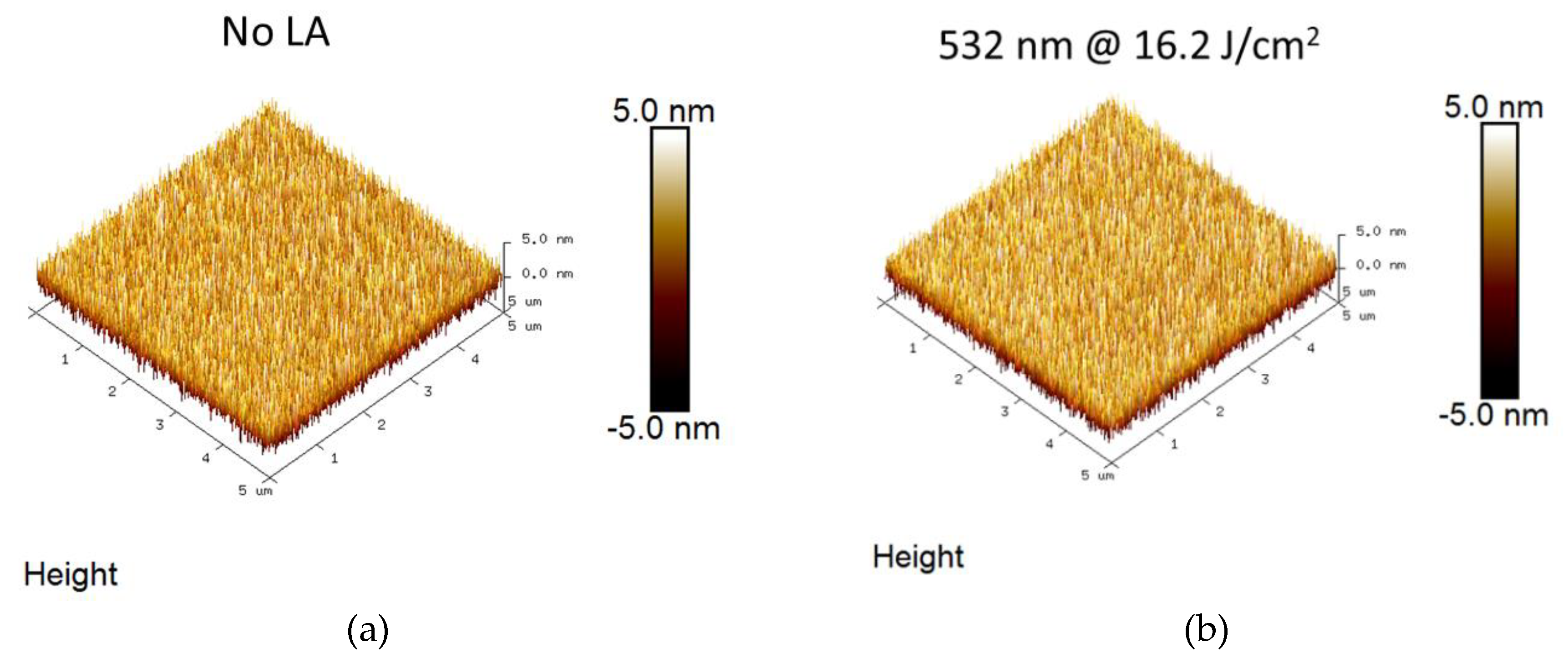
The surface morphology of ZrO2 before and after laser annealing samples is studied by AFM images, as shown in Figure 8 (a) and (b) using 5 µm × 5 µm scans. The root-mean-square roughness of ZrO2 before laser annealing was found to be around 1.14 nm, whereas the roughness of the ZrO2 after 532 nm laser annealing using 16.2 J/cm2 was 1.25 nm. In the process of laser annealing, the raise in temperature enables the grain boundaries migration and causes more grains coalescence. More energy is available for the atoms to diffuse and lower surface energy grains get enlarge at high temperatures. The major growth in grain as observed from XRD analysis highlights the enhanced surface roughness for the laser annealed of ZrO2 samples.
4. Conclusions
A high-performance Ni/ZrO2/TiN device has been achieved, offering both increased capacitance density and low leakage current. MATLAB calculations confirmed that annealing temperature rises with increasing laser energy density, providing an alternative approach to achieve higher-κ dielectrics for next-generation MIM capacitors without the need to constantly introduce new materials.
Author Contributions
Conceptualization, Wei Ting Fan and Albert Chin; methodology, Wei Ting Fan; software, Pheiroijam Pooja; validation, Wei Ting Fan, Pheiroijam Pooja and Albert Chin; formal analysis, Wei Ting Fan; investigation, Wei Ting Fan; writing—original draft preparation, Pheiroijam Pooja; writing—review and editing, Albert Chin; supervision, Albert Chin. All authors have read and agreed to the published version of the manuscript.
Funding
This work was supported by the National Science and Technology Council of Taiwan [Project no. 113-2221-E-A49 -100 and 113-2811-E-A49 -534] for the research.
Data Availability Statement
The data presented in this study are available on request from the corresponding author. The data are not publicly available due to privacy.
Acknowledgments
We would like to thank the National Yang Ming Chiao Tung university nano facility center for providing the laboratory instruments.
Conflicts of Interest
The authors declare no conflict of interest.
References
- Kashir, A.; Farahani, M.G.; Kamba, S.; Yadav, M.; Hwang, H. Hf1-xZrxO2/ZrO2 nanolaminate thin films as a high-k dielectric. ACS Appl. Electron. Mater. 2021, 3, 5632–5640. [Google Scholar] [CrossRef]
- Cheema, S.S.; Shanker, N.; Wang, L.C.; Hsu, C.H.; et al. Ultrathin ferroic HfO2–ZrO2 superlattice gate stack for advanced transistors. Nature 2022, 604, 65–71. [Google Scholar] [CrossRef] [PubMed]
- Tang, X.; Li, Y.; Miao, S.; Chen, X.; Xu, G.; Lu, D.; Long, S. Oxidizer engineering of ALD for efficient production of ZrO2 capacitors in DRAM. IEEE Electron Device Lett. 2024, 45, 2114–2117. [Google Scholar] [CrossRef]
- Hong, M.; Dawkins, R.B.; Bertoni, B.; You, C.; Magana Loaiza, O.S. Nonclassical near-field dynamics of surface plasmons. Nat. Phys. 2024, 20, 830–835. [Google Scholar] [CrossRef]
- Yu, D.S.; Chin, A.; Laio, C.C.; Lee, C.F.; Cheng, C.F.; Chen, W.J.; Zhu, C.; Li, M.F.; Yoo, W.J.; McAlister, S.P.; Kwong, D.L. 3D GOI CMOSFETs with novel IrO2(Hf) dual gates and high-k dielectric on 1P6M-0.18μm-CMOS. In IEDM Technical Digest. IEEE International Electron Devices Meeting, San Francisco, CA, USA, 13-15 December 2004.
- Shih, C.W.; Chin, A.; Lu, C.F.; Yi, S.H. Extremely high mobility ultra-thin metal-oxide with ns2np2 configuration. IEEE International Electron Devices Meeting (IEDM), Washington, DC, USA, 07-09 December 2015.
- Chin, A.; Chen, Y.D. Technologies toward three-dimensional brain-mimicking IC architecture. Electron Devices Technology and Manufacturing Conference (EDTM), Singapore, 12-15 March 2019.
- Sathyaseelan, B.; Manikandan, E.; Baskaran, I.; Senthilnathan, K.; Sivakumar, K.; Moodley, M.K.; Ladchumananandasivam, R.; Maaza, M. Studies on structural and optical properties of ZrO2 nanopowder for opto-electronic applications. J. Alloys Compd. 2017, 694, 556–559. [Google Scholar] [CrossRef]
- Wilk, G.D.; Wallace, R.M.; Anthony, J.M. High-k gate dielectrics: Current status and materials properties considerations. J. Appl. Phys. 2001, 89, 5243–5275. [Google Scholar] [CrossRef]
- Zhang, J.; Chen, T.P.; Li, X.D.; Liu, Y.C.; Liu, Y.; Yang, H.Y. Investigation of localized surface plasmon resonance of TiN nanoparticles in TiNxOy thin films. Opt. Mater. Express. 2016, 6, 2422–2433. [Google Scholar] [CrossRef]
- Kharitonov, A.; Kharintsev, S. Tunable optical materials for multi-resonant plasmonics: from TiN to TiON. Opt. Mater. Express. 2020, 10, 513–531. [Google Scholar] [CrossRef]
- Lu, H.L.; Sun, L.; Ding, S.J.; Xu, M.; Zhang, D.W.; Wang, L.K. Characterization of atomic-layer-deposited Al2O3/GaAs interface improved by NH3 plasma pretreatment. Appl. Phys. Lett. 2006, 89, 152910. [Google Scholar] [CrossRef]
- Edwards, A.P.; Mittereder, J.A.; Binari, S.C.; Katzer, D.S.; Storm, D.F.; Roussos, J.A. Improved reliability of AlGaN-GaN HEMTs using an NH3 plasma treatment prior to SiN passivation. IEEE Electron Device Lett. 2005, 26, 225–227. [Google Scholar] [CrossRef]
- Chiang, K.C.; Cheng, C.H.; Jhou, K.Y.; Pan, H.C.; Hsiao, C.N.; Chou, C.P.; McAlister, S.P.; Chin, A.; Hwang, H.L. Use of a High-Work-Function Ni Electrode to Improve the Stress Reliability of Analog SrTiO3 Metal–Insulator–Metal Capacitors. IEEE Electron Device Lett. 2007, 28, 694–696. [Google Scholar] [CrossRef]
- Cao, Q.; Su, J. Study on thermal effect and thermal stress effect of multilayer thin films induced by pulsed laser. In Pacific Rim Laser Damage 2019: Optical Materials for High-Power Lasers, 8 July 2019.
- Chiang, K.C.; Chin, A.; Lai, C.H.; Chen, W.J.; Cheng, C.R.; Hung, B.R.; Liao, C.C. Very high K and high density TiTaO MIM capacitors for analog and RF applications. In Digest of Technical Papers. 2005 Symposium on VLSI Technology, Kyoto, Japan, 14-16 June 2005.
Figure 2.
Temperature profile of TiN/ZrO2 samples under 532 nm laser of (a) 5.4 J/cm2 and (b) 16.2 J/cm2 and (c) 21.6 J/cm2.
Figure 2.
Temperature profile of TiN/ZrO2 samples under 532 nm laser of (a) 5.4 J/cm2 and (b) 16.2 J/cm2 and (c) 21.6 J/cm2.
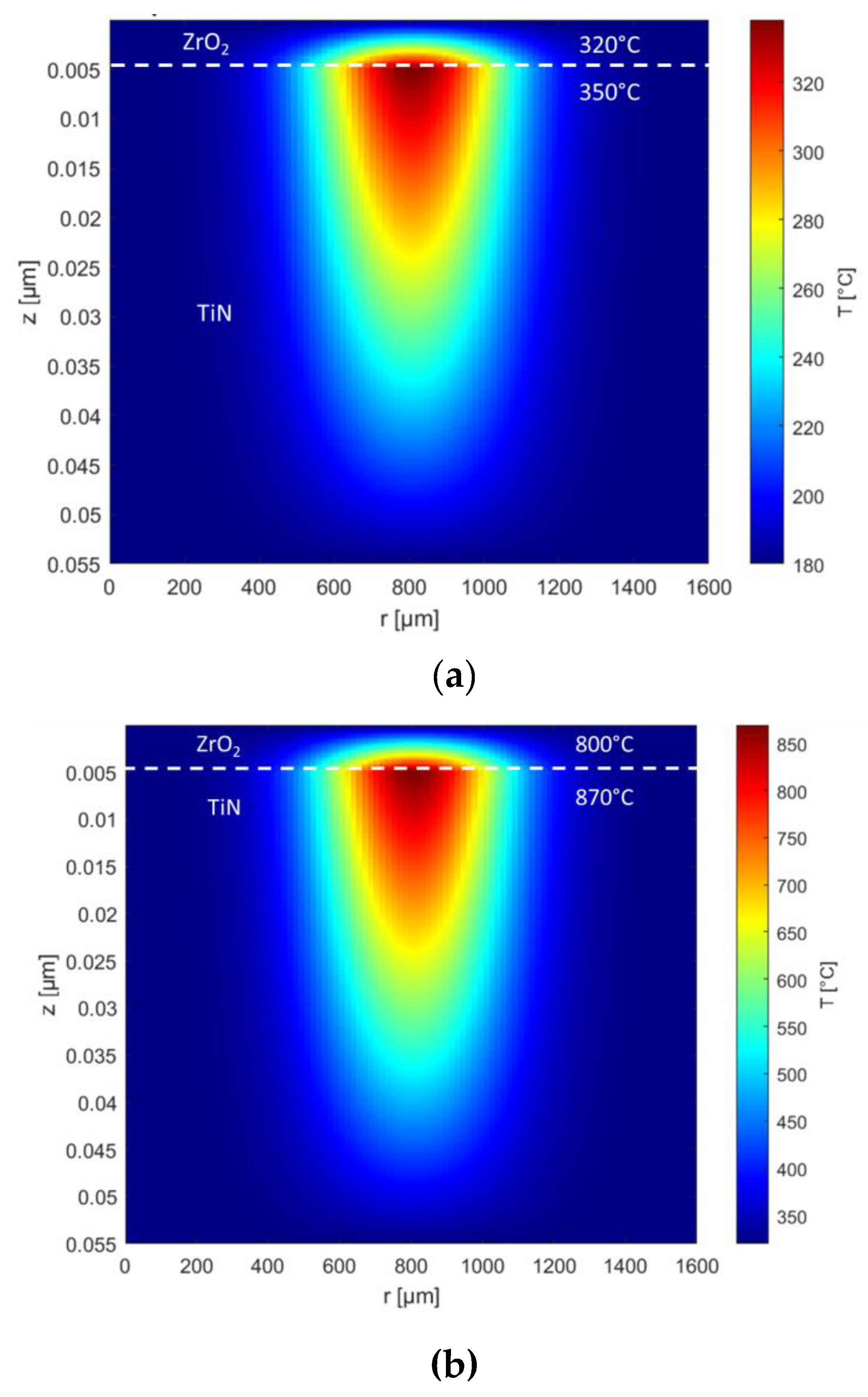
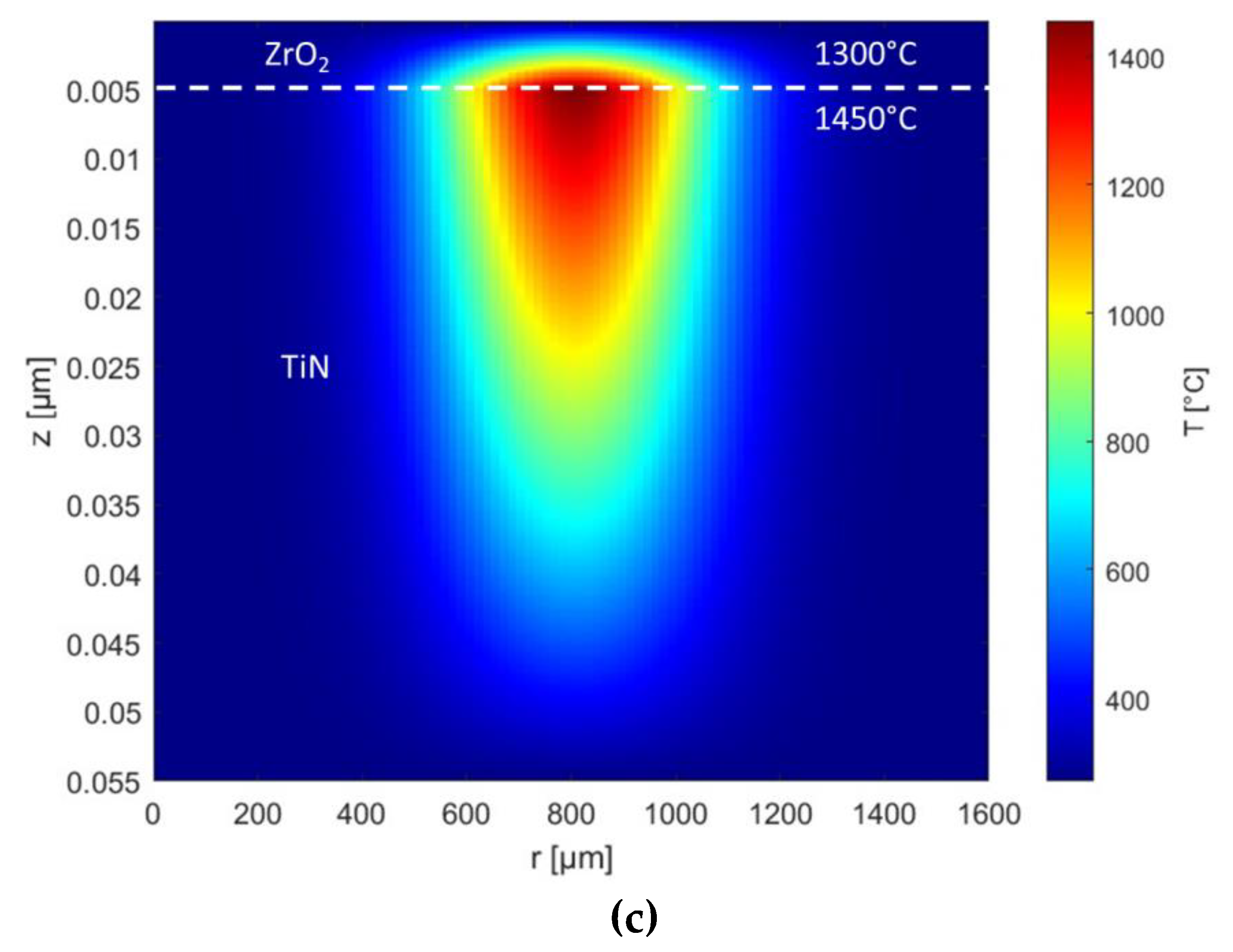
Figure 3.
C–V of Ni/ZrO2/TiN MIM capacitors under NH3+ plasma conditions (a) 2000 W 60s, (b) 2000 W 120s, (c) 2400 W 60s and (d) 2800 W 60s (LA: Laser annealed).
Figure 3.
C–V of Ni/ZrO2/TiN MIM capacitors under NH3+ plasma conditions (a) 2000 W 60s, (b) 2000 W 120s, (c) 2400 W 60s and (d) 2800 W 60s (LA: Laser annealed).
Figure 4.
J–V characteristics of the Ni/ZrO2/TiN (LA: Laser annealed).
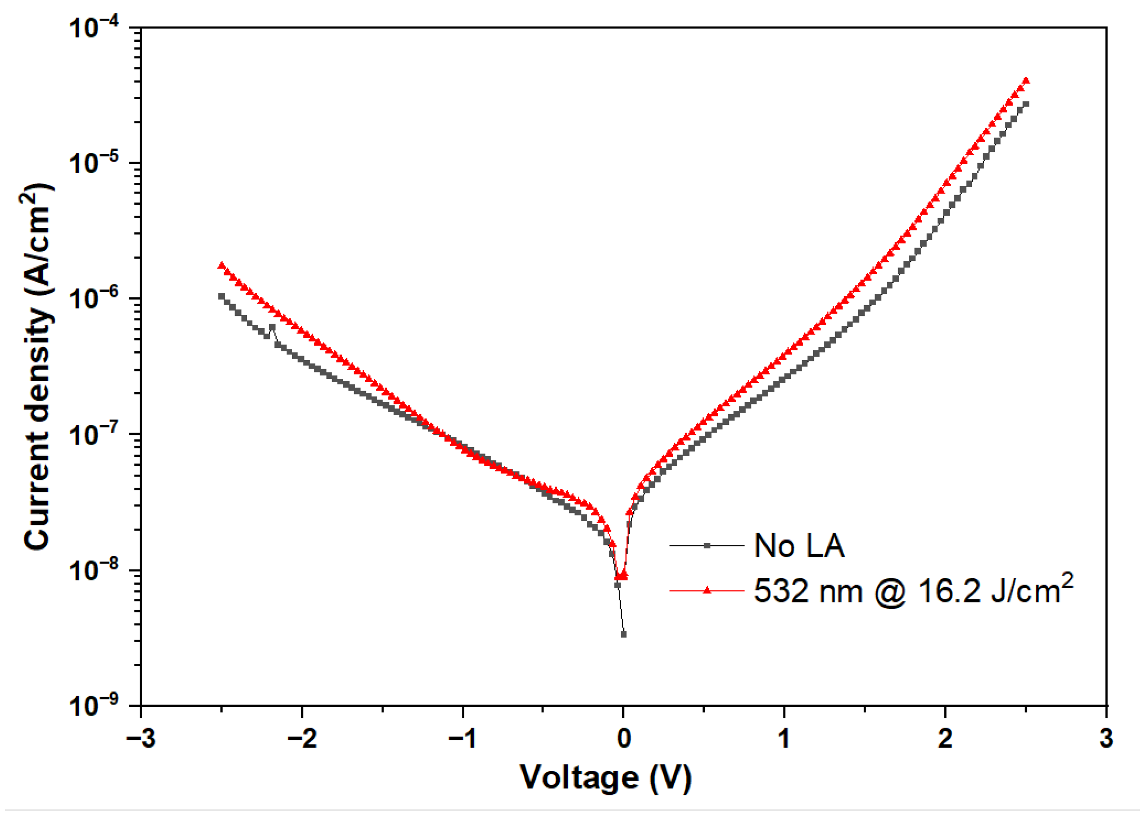
Figure 5.
Ni/ZrO2/TiN MIM capacitors laser annealed at 532 nm, 21.6 J/cm2 (a) C-V and (b) J-V characteristics.
Figure 5.
Ni/ZrO2/TiN MIM capacitors laser annealed at 532 nm, 21.6 J/cm2 (a) C-V and (b) J-V characteristics.
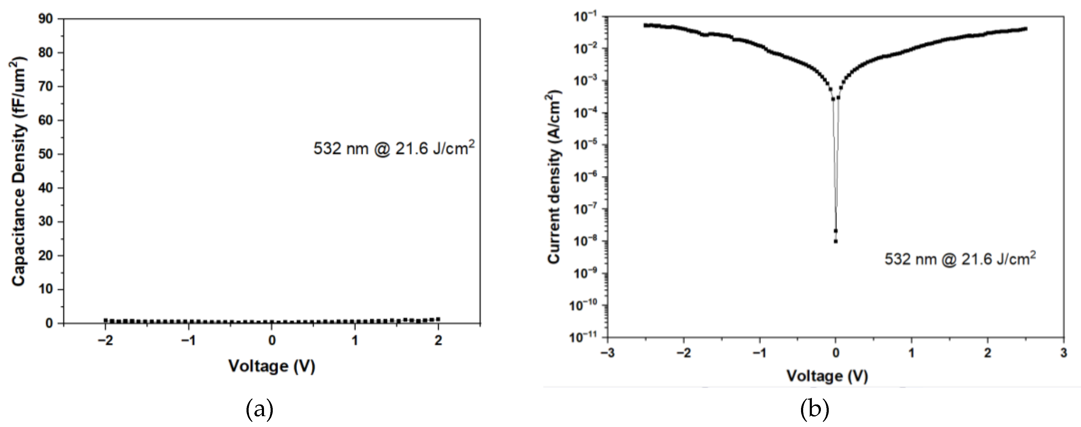
Figure 6.
XRD spectra of the Ni/ZrO2/TiN capacitors (LA: Laser annealed).
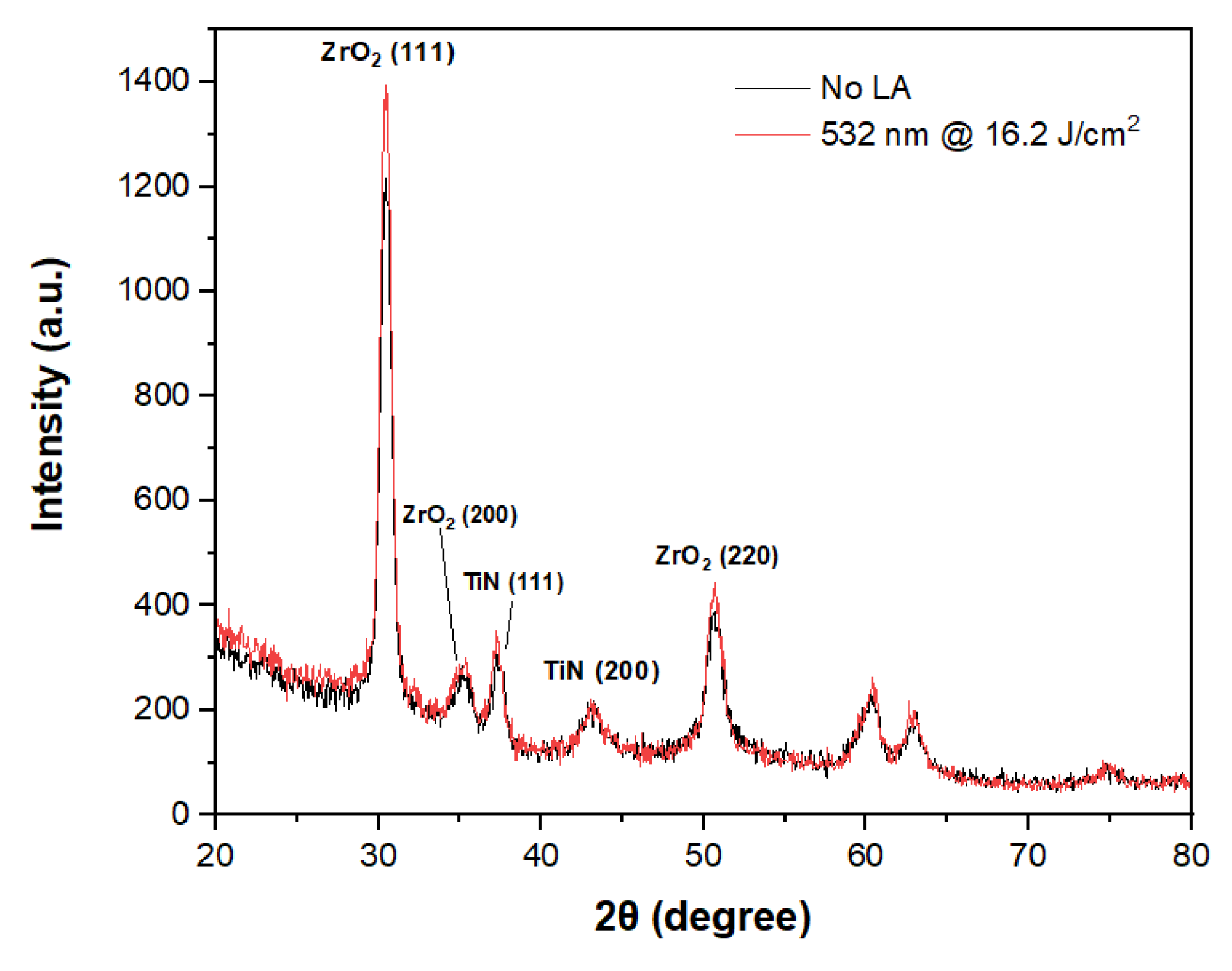
Figure 7.
TEM cross sectional image of the Ni/ZrO2/TiN capacitors (a) before and (b) after laser annealing.
Figure 7.
TEM cross sectional image of the Ni/ZrO2/TiN capacitors (a) before and (b) after laser annealing.
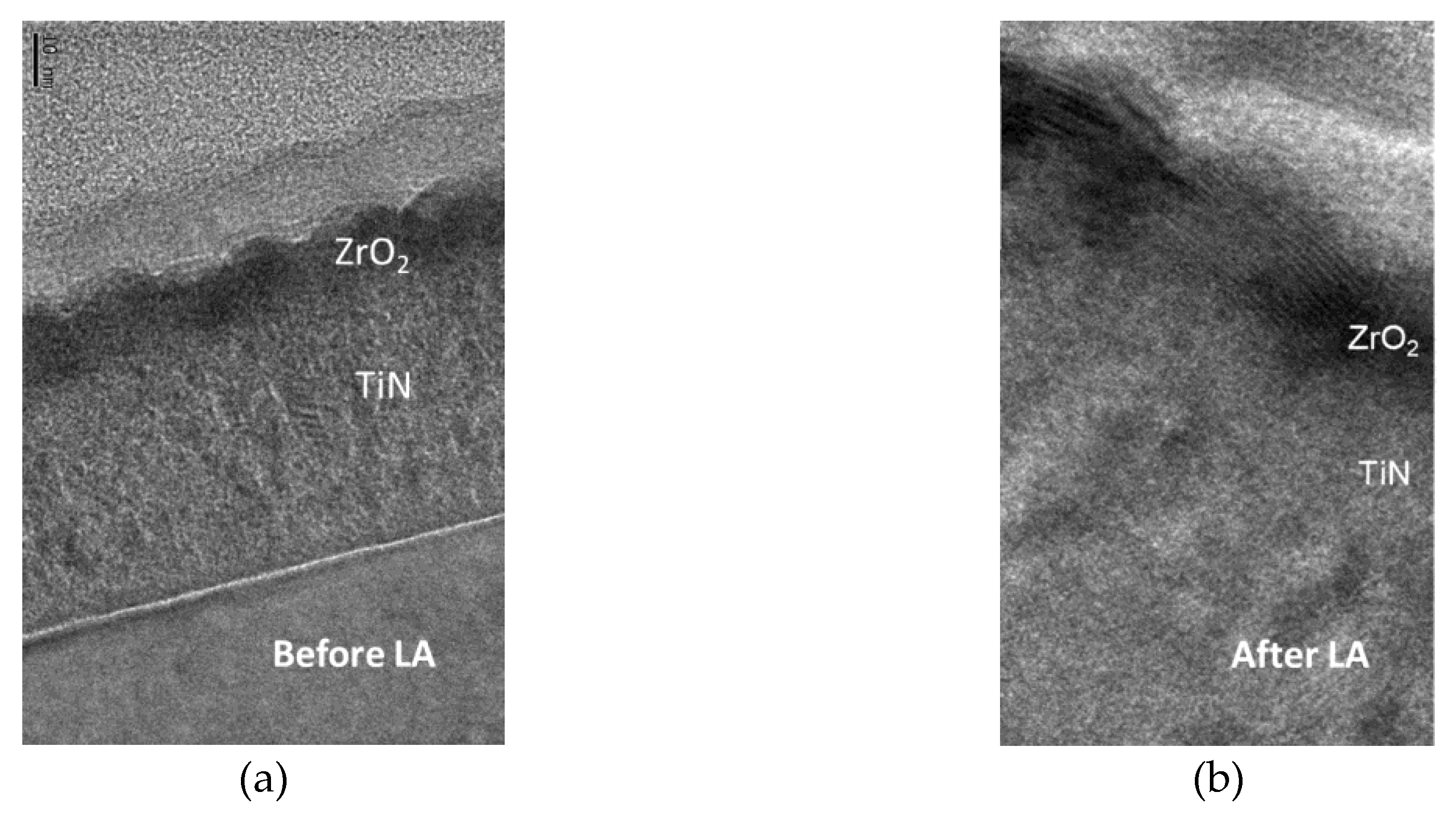
Figure 8.
AFM images wide scans spectra of (a) No LA and (b) 532 nm LA, 16.2 J/cm2 (LA: Laser annealed).
Figure 8.
AFM images wide scans spectra of (a) No LA and (b) 532 nm LA, 16.2 J/cm2 (LA: Laser annealed).
Disclaimer/Publisher’s Note: The statements, opinions and data contained in all publications are solely those of the individual author(s) and contributor(s) and not of MDPI and/or the editor(s). MDPI and/or the editor(s) disclaim responsibility for any injury to people or property resulting from any ideas, methods, instructions or products referred to in the content. |
© 2024 by the authors. Licensee MDPI, Basel, Switzerland. This article is an open access article distributed under the terms and conditions of the Creative Commons Attribution (CC BY) license (http://creativecommons.org/licenses/by/4.0/).
Copyright: This open access article is published under a Creative Commons CC BY 4.0 license, which permit the free download, distribution, and reuse, provided that the author and preprint are cited in any reuse.


