
Submitted:
03 December 2024
Posted:
06 December 2024
You are already at the latest version
Abstract
Scanning Photoelectron Microscopy (SPEM) experiment has been applied to ZnO:N films deposited by Atomic Layer Deposition (ALD) under O-rich conditions and post-growth annealed in oxygen at 800oC. State of the Art spatial resolution (130 nm) allows probing electronic structure of single column of growth. The samples were cleaved under ultra-high vacuum (UHV) conditions to open atomically clean cross-sectional area for SPEM experiment. It has been shown that different columns reveal considerably different shape of the valence band (VB) photoemission spectra, and some of them are shifted towards the bandgap. The shift of the VB maximum, which is associated with hybridization with acceptor states, was found to be correlated with carbon content measured as a relative intensity of the C1s and the Zn3d core levels. Density Functional Theory (DFT) calculations of V_Zn migration properties suggest that interstitial -CH_x groups facilitate the formation of acceptor complexes due to additional lattice perturbation.
Keywords:
ZnO
; p-doping
; photoelectron microscopy
; density functional theory
1. Introduction
The p-type conductivity of ZnO has been the subject of extensive research for over 20 years. Although the problem has not yet been solved, the systematic studies combining modern research techniques supported by advanced theoretical calculations and tailored growth technology provide interesting new results. An important step forward was finding that the electron concentration of undoped ZnO layers is not determined solely by the native defects or hydrogen impurity, but defect clusters containing both these components, such as H, H or n, n, which was both predicted theoretically [1] as well as observed by many experimental techniques such as FTIR [2], Raman spectroscopy [3,4] or positron annihilation spectroscopy [5,6]. These defect clusters introduce deep and shallow levels in the bandgap, mostly donor-type, which explains a wide range of electron concentration values that for undoped materials take values from 1014 till 1020/cm3 depending on growth conditions [7,8]. Consistently, p-type conductivity of ZnO is also closely associated with defect clusters, which in addition to native defects ( in this case) also contain a dopant atom and sometimes hydrogen. For nitrogen, which is considered to be the best acceptor dopant in ZnO due to its ionic radius and ionization energy similar to oxygen, defect clusters such as N, -NO-Hx or (NO-Hx)Zn are considered [1,9] , and these complexes may be formed in ZnO in many different ways depending on growth conditions. Since the formation of such clusters is much more complicated than the simple introduction of a substitutional dopant, the question arises whether such clusters can be formed in a controlled manner during the growth and/or post-growth processing of ZnO. The situation is even more complex since the macroscopically measured p-type conductivity of ZnO may have a complicated microscopic origin, as shown by recent low temperature cathodoluminesence (LTCL) and scanning photoelectron spectroscopy (SPEM) studies that reveal separated donor and acceptor regions in ZnO:N [10,11,12]. Additionally, the separated micro-regions with different conductivity type have been also found in the surface photovoltage measurements of N-doped and N-As co-doped ZnO nanoparticles (NPs) [13,14].
The reasons for the formation of donor and acceptor domains in ZnO are not clear, but it can be hypothesized that the distortion of the crystal lattice and the associated strain play a certain role. Defect complexes involve specific structural changes in the crystal lattice, so they it can be assumed that the appropriately introduced microstrain and also surface proximity may facilitate their formation. The recent first-principle calculations indicate that the strain effect might be responsible for the formation of VZn-H acceptor complexes which in undoped ZnO can be formed in crystallites exhibiting compressive strains or near the surface.[15] In support to theoretical results, the low-temperature PL spectra measurements have shown considerably varying acceptor luminescence intensities for the samples with different crystallographic orientation and strain.[15]
In the present studies we show that not only the strain/microstrain conditions inside the ZnO:N film, but also the carbon incorporation may be an important factor facilitating the formation of acceptor complexes in ZnO. Carbon, similarly to hydrogen, is a common impurity in ZnO that cannot be avoided in most of the growth procedures. The role of carbon has been already described in a series of theoretical and experimental works. Some groups reported p-type conductivity for C-doped ZnO [16,17], but others delivered contradictory results [18,19,20]. Sakong and Kratzer [21], based on Density Functional Theory (DFT) calculations, considered charged carbon impurities in ZnO and found to be the most stable configuration for a wide range of Fermi level positions. They found out it to be a double donor for lower EF position which converts to an acceptor for EF higher than 2.5 eV. However, these calculations yielded a ZnO bandgap of 1.65 eV, which challenges this finding. In turn, DFT calculations of Lyons [22] et al. confirm that is the most stable configuration in ZnO and show that it always acts as a double donor. In fact, recent research reveals the opening of the ZnO bandgap upon carbon doping and relative increase of electron concentration, indicating the occurrence the Burnstein-Moss effect.[23] However, it should be mentioned as well that there are experimental evidences that carbon can be passivated by hydrogen by forming the C-H complex, which is stable up to 1000 °C in the ZnO lattice [24]. On the other hand, there are also indications of stable C-N complexes with a low formation energy in ZnO doped with nitrogen.[25,26] It has been shown that the presence of carbon facilitates the incorporation of nitrogen, the amount of which in this case can reach up to several percent. [26] Additionally, DFT calculations of Liu et al. [27] demonstrate that the localized states of the origin appear near to the Fermi level, leading to the bandgap narrowing.
The SPEM investigations reported here show the modification of the valence band maximum (VBM) in ZnO doped with nitrogen, both and post-grown annealed. Photoemission spectra taken with resolution of 130 nm at different points of the ZnO:N film cross-section show the correlation of the VB shape and position with the carbon content. The low-intensity shape of the VBM and its shift towards the bandgap, characteristic of acceptor domains [12] has been observed for crystallites with high carbon content.
According to a number of theoretical works,[1,12] in the presence hydrogen, the -NO-Hx is the dominant acceptor complex in ZnO:N which introduces a deep acceptor state in the middle of bandgap. [1] On the other hand, the -NO pair, which is a shallow acceptor with the ionization energy of about 0.17 eV, [9,12] could be created by the annealing process by removing hydrogen from the -NO-Hx complex[10,12]. Recent DFT calculations reveal that the complexes involving zinc vacancy () and nitrogen substituting oxygen (NO) modify the valence band maximum states (VBM) and, in case of the -NO pair, the VBM is moved towards the bandgap [12]. DFT calculations presented here provide evidence that -CH and -CH2 groups facilitate the formation of the above-mentioned acceptor defect complexes in the ZnO:N material.
2. Methods
Deposition of ZnO:N thin films Nitrogen-doped zinc oxide films were grown on a Si(100) substrate by Atomic Layer Deposition (ALD) using a commercial Savannah-100 reactor from Cambridge Nanotech. The details of the growth process can be found elsewhere.[11] The films were deposited at 100 °C using a pulse time of 20 ms for both deionized water and dimethylzinc precursors, while the nitrogen purging was set at 2 s. Such a low deposition temperature of the ALD process assures high oxygen content in the layer [8] and promote the formation of zinc vacancy. Nitrogen was introduced into the films using an ammonia water (NH4OH) precursor alternating with a deionized water precursor every 4th ALD cycle, resulting in a N-doping level of 1·1019at/cm3. The ALD growth was performed for 10000 cycles, giving the layer thickness of about 2.0 µm. Post-growth Rapid Thermal Annealing (RTA) in oxygen atmosphere (800 °C, 3 min.) was performed in an AccuTherm AW610 system from Alwin21 Inc. The goal of RTA was to remove excess hydrogen and allow the deep -NO-H acceptor levels to be converted to shallow levels of -NO origin [10,11,12]. The annealing conditions were selected based on cathodoluminescence (CL) studies aimed at generating abundant acceptor centers in ZnO:N layers [10]. As previously shown, ZnO samples grown by ALD have high hydrogen content that decreases after RTA to the level of 1019/cm3 [8,10]. The samples reveal the wurtzite-type crystal structure and show polycrystalline nature with dominating 100 and 110 peaks, and transmission electron microscopy shows a columnar structure with ordered rows of atoms inside the grains [11].
Scanning Photoelectron Microscopy measurements
The SPEM experiment was performed on the ESCA Microscopy beamline (Elettra, Trieste, Italy) with photon energy of 650 eV and energy resolution of 300 meV [28,29]. The spatial resolution of 130 nm, which is in scanning photoemission experiments, allowed for separate study of the electronic structure of each single growth column. The samples were cleaved inside a photoemission chamber under ultrahigh vacuum (UHV) conditions, which allowed for obtaining an atomically clean cross-sectional area. The photoemission experiment was performed , immediately after cleavage. The experimental configuration is shown in Figure 1.
Computational methods The generalized gradient approximation (GGA) [30] was performed using the +U corrections [31] implemented in the QUANTUM-ESPRESSO package (QE)[32]. We employed ultrasoft atomic pseudopotentials [33] with the following valence orbitals of Zn(3,4) O (2, 2), N(2, 2), C(2, 2), and H(2, 1) and the plane waves kinetic energy cutoff of 40 Ry for wave functions. We used the wurtzite 128-atom supercell and optimized atomic positions. For the supercell, the k-space summations are performed with a 2×2×2 k-points grid [34] or with a -point. The +U terms of 10 and 7 eV were applied to the d ( of Zn) and p (of O, N, C) orbitals, respectively [12]. These values give the ZnO lattice parameters ( = 3.223 Å and = 5.24 Å) that are consistent with the experimental data, and the correct band structure of the material[12]. In particular, the calculated energy of forbidden gap, Eg =3.4 eV, agrees well with the experimental results.
The defect migration properties were obtained by the nudged elastic band (NEB) method implemented within the QE.[32]
Formation energies (Eform) for O-rich conditions are calculated according to Ref. [35] and details are given in Ref. [12].
where (CiHx:ZnO) and (ZnO) are the total energies of the supercell with and without the neutral CiHx, respectively. and are the chemical potentials of C and H in the solid and are referenced to the energies of bulk C (diamond-structure) and per atom of an isolated H2 molecule, respectively.
3. Experimental Results
The cleavage area was investigated taking the imaging mode [28] of the ZnO:N/Si(100) film cross-section. We investigated both ZnO:N/Si film as well as the same film after 3 min. annealing in oxygen atmosphere at 800 °C. Such annealing conditions were found the most optimal for the activation of shallow acceptor states based on the cathodoluminescence studies of acceptor emission from ZnO:N films deposited in a similar ALD process.[10]
Since the samples were mechanically broken inside the photoemission chamber, the cleavage area was not fully uniform and some parts of the cross-section are more or less exposed to the SPEM measurement (Figure 2a). As can be seen, the cross-sectional image of the ZnO:N layer is qualitatively similar to that obtained in a scanning electron microscope (SEM)[36], and individual growth columns are easily distinguishable.
In the next step, the general photoemission (PES) spectra as well as the valence band with the core level, the and spectra were measured at selected points of the cross-section area, as marked with black letters in Figure 2a. Before collecting the PES spectra, the Au foil being in electrical contact with the ZnO:N sample was measured and the energy scale was calibrated to the binding energy of the core level (84.0 eV). This kind of calibrations means that zero on the energy scale is related to the Fermi level. In all presented spectra the background was subtracted assuming a Shirley background.
The PES signal from the core level was found below the detection limit because of a doping concentration (at the level of 1019/cm3 as measured by secondary ion mass spectrometry) as well as extremely small sampling area.
The PES spectra of ZnO:N film measured in the valence band (VB) and the core level region reveal a shift of the core level and different shape of the VB for measurements performed at different points of the film cross-section (Figure 2)b. The spectra were taken in many different points of the ZnO:N film cross-section, but for the clarity, four representative ones have been selected as shown in Figure 2.
The valence-band spectrum of zinc oxide origins from the hybridized and electron shells and consists of two maxima, one at about 5 eV and second at about 7.7 eV below the Fermi level. The most substantial difference between PES spectra taken at different points of the film cross-section (i.e. for different growth columns) is the shape of the VB peak located at 5 eV below the Fermi level, EF (see Figure 2b). The intensity of this maximum is about 30 percent higher for points O and R compared to points P and Q. The closer look at the VB edge (Figure 2d) shows that the spectra with lower intensity are slightly shifted towards the Fermi level, and this shift can be evaluated to be less than 100 meV. It is accompanied by a shift in the same direction of the core level, but the latter one is about twice higher. The Full Width at Half Maximum (FWHM) of the core level was found between 1.55-1.58 eV for the low-intensity spectra and 1.62-1.67 eV for the high-intensity spectra. A shift of the core level towards lower binding energy can be understood in terms of a change in the Madelung energy and is related to the shift of the VB positions towards the EF, which favors hybridization of the valence band with shallow acceptor states.
The same set of results was obtained for the same ZnO:N sample, but annealed at 800 °C in oxygen atmosphere (Figure 3). The cross-sections of annealed ZnO:N film and selected points where PES spectra were taken are shown in Figure 3a. The PES spectra in the VB and the binding energy region taken at points C, D, F and G are shown in Figure 3b. The PES spectra were also taken in the rest of marked points, but for clarity we choose the most representative ones for a comparison. Similarly as for the samples, after annealing we also observe two kind of shapes of the PES spectra in the VB region and a shift of the towards the Fermi level, however, the differences between and annealed samples are significant. First, the highest maxima at 5 eV are about 20 percent lower for the annealed sample (compare Figs. Figure 3b and Figure 2b), while the height of the maximum at 7.7 eV remains untouched. Second, a pronounced shift of the low-intensity spectra towards the Fermi level can be clearly seen at points F and G (Figure 3d). This shift reaches a value of about 350 meV, and all measured VB spectra can be divided into two types with respect to this shift; the low-intensity spectra are shifted towards the EF, while the high-intensity spectra are situated at higher binding energy. The accompanying shift of the level takes the same value of 350 meV. It is worth noting that in all cases the shift towards EF show only the low-intensity spectra. Such a shift of the VB edge towards the bandgap indicates hybridization of the valence band electrons with shallow acceptor states. In this respect, the lowering intensity of the maxima close to the VB edge can be regarded as a fingerprint of the formation of acceptor complexes involving nitrogen, zinc vacancy and, possibly, hydrogen. This finding has been supported by the recently published DFT calculations that show that -NO and -NO-H complexes in ZnO:N can modify density of states near the VB edge [12].
A deeper insight into this issue can be gained by analyzing the core level for and annealed samples. Deconvolution of the peak measured for the ZnO:N film (Figure 4) shows only one contribution of this peak at point O, and two of them at points P, Q and R. At point O the binding energy of the level is 531.17 eV, while for the rest of the points it is lower and equal to 530.74 eV. The additional contribution, visible at points P, Q and R, is located at a binding energy about 1 eV higher. The main peak comes from oxygen bound to zinc in the ZnO lattice. Comparison of the binding energy of the high-BE contribution with the reference book of standard photoemission spectra [37] and with previously published results for ZnO films obtained by ALD [8] indicates that it comes from oxygen bound to carbon. Indeed, since the ALD growth of ZnO layer uses the metalorganic precursor diethylzinc (DEZn), we can expect little carbon contamination. In fact, deionized water is also used in the ALD growth process, so some contribution to the peak from -OH groups cannot be excluded, especially because according to the Reference Book of Standard Spectra [37] the contribution from -OH groups can be expected in a similar BE range. However, comparing the present spectra with the previously published ones [8] we see that the high-BE contributions shown in Figure 4 are relatively small and therefore it is difficult to judge whether they consist of one peak or two.
This small high-BE contribution is related to the way of performing the photoemission measurement, which was done on an atomically clean surface, created by cleaving the sample in vacuum, while typically XPS spectra are taken from the surface, where there is an additional contribution from adsorbed CO2 molecules. These molecules remain on the surface even after sputtering and are visible in the photoemission spectra due to extremely high surface sensitivity of this technique (sampling depth of 2-3 nm). In this sense, the spectrum measured at point O, like the spectra for points C and D presented in Figure 5, showing exclusively the signal from oxygen bound to the lattice zinc atoms with no additional contributions, are unique and have not been presented for ZnO films before.
A significant difference in the spectra is visible after annealing (Figure 5). In this case we observe two types of spectra. For measurements performed at points C and D, we see only a single peak situated at BE of 531.0 eV, while at points F and G the BE of this peak is lower (530.65 eV) and two additional contributions are visible. The contribution at higher BE appears at 532.6 eV, which is very similar to the BE of this peak observed for sample. Moreover, the intensity of this peak compared to the main peak, is also similar. This similar dependence of the contributions at higher binding energy for annealed and unannealed samples supports the assignment to the oxygen atoms bonded to carbon, since previously published results clearly indicate the disappearance of -OH groups after annealing of ZnO layers in oxygen at 800°C [38]. A very interesting effect is the appearance of the contribution at lower BE of 529.3 eV, visible at points F and G. To our best knowledge, such a low-BE contribution has never been reported for ZnO films. According to Moulder [37] , such a low BE of the level is expected for oxygen atoms in metal oxides. Since the main peak already comes from oxygen bound to metal (zinc) atoms in the ZnO lattice, we assumed another origin of this contribution and tentatively assigned it to oxygen atoms in vicinity of acceptor complexes that are expected to be formed in ZnO:N film grown in O-rich conditions and annealed in oxygen [12]. This hypothesis is supported by the valence band shift towards a bandgap that is observed in the photoemission spectra taken at the same F and G points (see Figure 3d). Interestingly, the spectra collected at points C and D, located at higher BE of 531.0 eV, do not show any contributions to the main peak. Accordingly, the valence band spectrum measured at these points is also shifted towards higher BE (see Figure 3d).
The analysis of the valence band shift for all the examined cross-section points show a strong correlation between the carbon content and the valence band shift towards the energy gap, which can be assigned to hybridization of valence band edge with shallow acceptor states. The theoretical calculations and discussion presented below aim to explain the role of carbon in the formation of acceptor states in nitrogen-doped ZnO.
4. Discussion
In our previous study[12], from both experimental and theoretical point view, it has been suggested that the moderation of the valence band maximum (VBM) of ZnO:N and the VBM shift towards the bandgap is associated with the shallow acceptor states of the VZnNO complexes. These complexes may be a product of dissociation reactions of VZnNOHx groups as a result of annealing processes and associated with the expulsion of H+ from the samples.[10] Moreover, the formation of the VZnNOHx groups depends on many factors of the deposition process, but as shown, they are easily formed during the ALD growth with an ammonia water precursor.[10] The experimental results presented above show that unintentional carbon doping affects the shift of the PES spectra, therefore we would like to understand the role of C impurity in this phenomena. This effect may have several different origins such as the introduction of defect states in the vicinity of the VBM or, alternatively, favoring the formation of VZnNO and/or VZnNOHx and/or C-VZnNOHx complexes or by introducing additional distortions into the crystal lattice,[15] or finally hydrogen absorption on the surface. [39] The last mechanism is unlikely in our experiments as C ions appear in the form of the CHx groups already during the growth process.[8] There is a number of important first-principles studies suggesting that C impurity in ZnO predominantly occurs via Zn ion substitution[21,22,40] or as interstitial lattice site (Ci),[21,40] particularly under O-rich conditions which is the case of our growth process. The CZn ion can be regarded as a plausible candidate for a shallow donor dopant.[22] Moreover, the experiment[23] showed that with C doping there is a gradual increase in optical Eg, indicating the typical Burstein-Moss effect.
Here, we study the Ci, Ci-Hx (x= 1, 2) and CiHx–VZnNOHx complexes in terms of their structural stability, migration properties, and electronic properties. We note that the formation energies and computed Density of States (DOS) of VZnHx, VZnBOHx and VznNO complexes have been studied in our earlier works.[12,15] To find equilibrium configurations of defects, a few initial locations of atoms were checked. The obtained equilibrium configurations of Ci and complexes are shown in Figure 6. In the equilibrium geometry both Ci and Ci-Hx bind to neighboring O atoms, forming C-O complexes (see Figure 6a-c). This is reflected in the their electronic wave distributions that are depicted in Figure 6a,b by yellow color. The above C-O bonding states are also observed in core-level XPS spectra (Figure 4 and Figure 5). The gain, Egain, in the formation energy of the complexes is evaluated as the difference in the formation energy between isolated constituents of the complex and the complex itself for a given Fermi level. A positive value of Egain corresponds to a situation where there is an energetic preference for the defect complex to be formed. The calculations have shown that these complexes are energetically stable by 3.2, 3.5 and 4.5 eV for Ci-H, Ci-H2 and CiH–VZnNO, respectively. We note that in the last case of Ci-H at an interstitial site the defect complex engaging both a nearby Zn-vacancy and substituted nitrogen at O-site is formed. Complexes of the Ci-VZn type in carbon implanted ZnO nanowires were proposed early in Ref. [41] as an origin of the observed magnetic properties. Thus, the formation of CiH–VZnNO may support the hypothesis that the presence of carbon-hydrogen groups may promote the clustering of acceptor-complexes.
Next, we study the migration paths of zinc vacancy in ZnO and around the (NH)O complex in N-doped ZnO under two conditions: without and with the presence of CH2 groups in the samples. Within the NEB method, we calculate the diffusion paths for the exchange between zinc vacancy and its neighboring Zn atoms. Although there are two types of non-equilibrium paths, as one path is in the - plane and the other is along the c-axis, calculations have shown, that in undoped ZnO the two types of paths differ by less than 10 meV. Therefore, in Figure 7 we report the results for the first path only, the VZn migration from initial (IS) to final (FS) states. In Figure 7a-d, E were calculated with respect to the energies of a system in their ISs. Both, ISs and FSs for Zn vacancy migration paths around (NH)O both without and with the presence of CH2 are shown in Figure 7e-h. Therefore, FSs correspond to the equilibrium configuration of NOH complexes in both cases. The migration energy, i.e. the energy barrier, Em, is defined as the difference in energy between the IS and the energy of so the called the transition state (TS). Energy of TS corresponds to the highest energy point of the lowest energy migration path with respect to the IS-energy, i.e., Em = E(TS) - E(IS). Moreover, the positive difference between IS - and FS - energies may indicate the energetic preference for the defect complex to be formed. We found, that in undoped ZnO, Em of is 1.33 eV, as displayed in Figure 7a, that is in reasonable agreement with other DFT results and experimental measurements.[42]. Similarly, we calculate the diffusion path of VZn around(NH)O in N-doped ZnO. We found that VZn can recombine with a neighboring (NH)O group to form a VZnNOH complex by overcoming Em of about 0.65 eV, as displayed in Figure 7c. Next, we study the effect of the CHx interstitial groups in the samples on the energy of migration barrier of VZn in both ZnO and N-doped ZnO. In this vein, we calculated vacancy migration paths affected by the presence of CH2 group acting as interstitial impurities. We simulated the effect of local crystal deformations by randomly introducing a CH2 group separated from the vacancies by about 6 Å(see Figure 7g, h). Figure 7b,d present these migration paths that show that the migration barrier is reduced by 0.8 and 0.65 eV compared to the case without the carbon group. Moreover, we showed that the difference between IS and FS energies increased and therefore the acceptor complexes are more stable in the samples with carbon atoms. We point that the energy barriers have decreased significantly due to the increased atomic lattice disturbances generated by carbon groups. It has been previously suggested that microstrain/strain can affect the acceptor clustering of acceptors in ZnO[10,15] The effect of the lattice deformation and the localization of defect states on defect migration properties was shown in Refs.[43,44]. Moreover, Ref.[45] suggested within the bonding analysis as in the cation exchange process the change of bonding energy can be dominated by the local lattice distortion contributions. We note, as an example, that the decreasing/increasing distance between O ions around vacancy leads to the increasing/decreasing electron-electron coupling. In particular, the outward displacement of O ions decreases the overlap between the broken bonds, and consequently reduces the exchange interaction. Thus, it is clear from Figure 7e-h that the displacement of atoms around vacancies is stronger in structures with CH2 groups. Moreover, this atomic displacement extends not only to the nearest neighborhood, but affects also the farther neighbors.
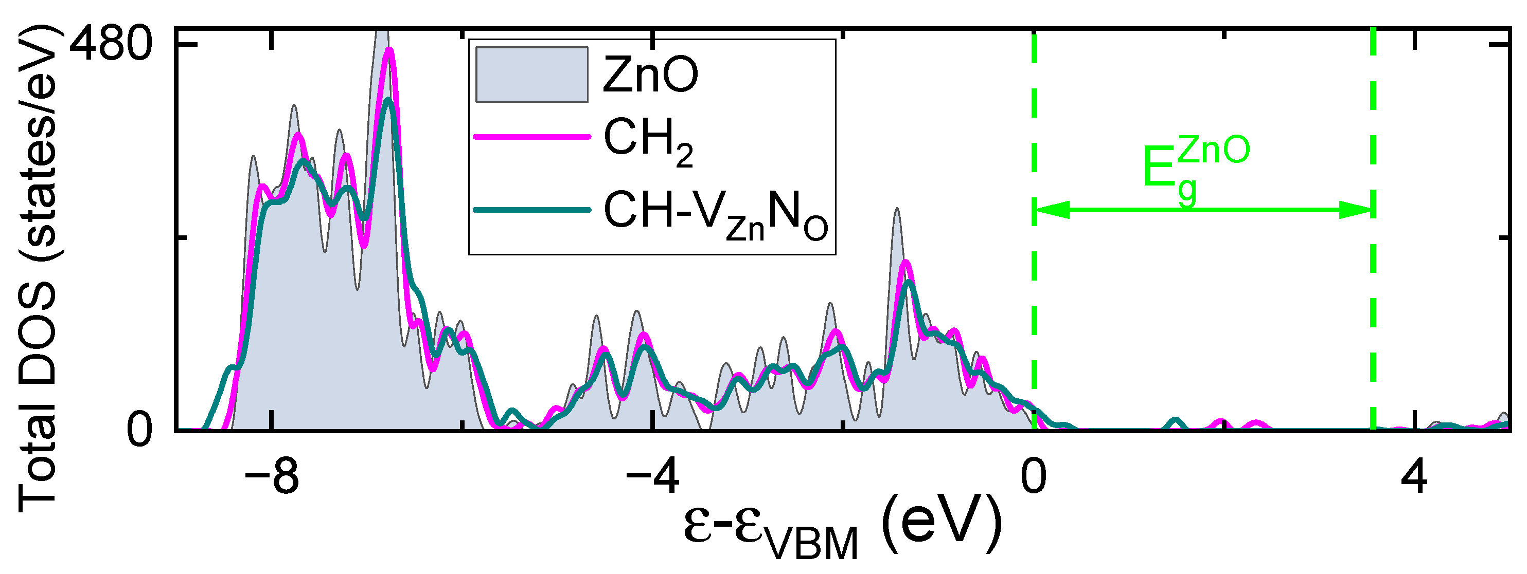
Finally, the calculated total DOSs (see Figure 8) are in agreement with the photoelectron spectra results. In particular, we see the core-level that is centered about 8 eV below the VBM. This level is slightly shifted towards the VBM for dopants in ZnO. From the other side, the shift of the VBM into more higher energies take place in the CiH-VZnNO complex case. At the same time, we do not see this effect in the case of the CiH2 group. Note that the CiH2 interstitial introduces defect states in the middle part of the bandgap, these states are occupied by electrons, and thus this complex is supposed to be a deep donor.
5. Summary
Photoelectron spectra of and annealed ZnO:N/Si films show significantly different intensity of the valence maximum close to the VB edge depending on the measured point of the film cross-section and a shift some of these spectra towards the bandgap pointing at hybridization with shallow acceptor states. A significant correlation between a valence band shift and carbon content has been found.
According to DFT calculations, CiHx is introduced into the ZnO lattice as a stable interstitial group that forms C-H-O bond states. This group causes the nearby Zn vacancy to "sense" the -NHO group in N-doped ZnO. Calculated migration properties show that complexes such as VZn(NH)O are easily formed in the presence of the interstitial CiH2 group. We suggest that this may be due to stronger disorder of the crystal lattice. This confirms that the formation of defect complexes is very sensitive to the local geometry and the lattice perturbations.
Acknowledgments
The work was supported by the project No. 2018/31/B/ST3/03576, founded by the National Science Centre (Poland). Calculations were done at Interdisciplinary Center for Mathematical and Computational Modeling, University of Warsaw. We acknowledge Elettra Sincrotrone Trieste for providing access to its synchrotron radiation facilities (proposal No. 20190499).
References
- Amini, M.; Saniz, R.; Lamoen, D.; Partoens, B. The role of the VZn-NO-H complex in the p-type conductivity in ZnO. Phys. Chem. Chem. Phys. 2015, 17, 5485–5489. [Google Scholar] [CrossRef] [PubMed]
- Senthilkumar, K.; Yoshida, T.; Fujita, Y. Formation of D-V(Zn) defects and possible p-type conductivity of ZnO nanoparticle via hydrogen adsorption. J. Mater. Sci. 2018, 53, 11977. [Google Scholar] [CrossRef]
- Gluba, M.A.; Nickel, N.H.; Karpensky, N. Interstitial zinc clusters in zinc oxide. Phys. Rev. B 2015, 88, 245201. [Google Scholar] [CrossRef]
- Pal, S.; Gogurla, N.; Das, A.; Singha, S.; Kumar, P.; Kanjilal, D.; Singha, A.; Chattopadhyay, S.; Jana, D.; Sarkar, A. Clustered vacancies in ZnO: Chemical aspects andconsequences on physical properties. J. Phys. D: Appl. Phys. 2018, 51, 105107. [Google Scholar] [CrossRef]
- Wang, L.; Chen, Z.; Liang, G.; Li, Y.; Lai, R.; Ding, T.; Wu, K. Observation of a phonon bottleneck in copper-doped colloidal quantum dots. Nat. Commun. 2019, 10, 1–8. [Google Scholar] [CrossRef] [PubMed]
- Makkonen, V.P.I.; Korhonen, E.; Tuomisto, F. Identification of vacancy defect complexes in transparent semiconducting oxides ZnO, In2O3 and SnO2. J. Phys.:Condens. Matter 2016, 28, 224002. [Google Scholar] [CrossRef]
- Schifano, R.; Jakiela, R.; Galeckas, K.K.A.; Johansen, K.; Vines, L. Role of intrinsic and extrinsic defects in H implanted hydrothermally grown ZnO. J. Appl. Phys. 2019, 126, 125707. [Google Scholar] [CrossRef]
- Guziewicz, E.; Godlewski, M.; Wachnicki, L.; Krajewski, T.; Luka, G.; Gieraltowska, S.; Jakiela, R.; Stonert, A.; Lisowski, W.; Krawczyk, M.; et al. ALD grown Zinc Oxide with controllable electrical properties. Semicond. Sci. Technol. 2012, 27, 074011. [Google Scholar] [CrossRef]
- Liu, Y.; Yao, D.; Shen, L.; Zhang, H.; Zhang, X.; Yang, B. Alkylthiol-Enabled Se Powder Dissolution in Oleylamine at Room Temperature for the Phosphine-Free Synthesis of Copper-Based Quaternary Selenide Nanocrystals. J. Am. Chem. Soc. 2012, 134, 7207. [Google Scholar] [CrossRef]
- Mishra, S.; Witkowski, B.S.; Jakiela, R.; Khosravizadeh, Z.; Paszkowicz, W.; Sulich, A.; Volnianska, O.; Wozniak, W.; Guziewicz, E. Cathodoluminescent Imaging of ZnO:N Films: Study ofAnnealing Processes Leading to Enhanced AcceptorLuminescence. Phys. Status Solidi A 2023, 220, 2200466. [Google Scholar] [CrossRef]
- Guziewicz, E.; Przezdziecka, E.; Snigurenko, D.; Jarosz, D.; Witkowski, B.; Dluzewski, P.; Paszkowicz, W. Abundant Acceptor Emission from Nitrogen-Doped ZnO Films Prepared by Atomic Layer Deposition under Oxygen-Rich Conditions. ACS Appl. Mat. Int. 2017, 9, 26143–26150. [Google Scholar] [CrossRef]
- Guziewicz, E.; Volnianska, O.; Demchenko, I.; Zeller, P.; Amati, M.; Gregoratti, L. Valence-Band Electronic Structure of ZnO and ZnO:N: Experimental and Theoretical Evidence of Defect Complexes. Phys. Rev. Applied 2022, 18, 044021. [Google Scholar] [CrossRef]
- Krtschil, A.; Look, D.; Fang, Z.Q.; Dadgar, A.; Diez, A.; Krost, A. Local p-type conductivity in n-GaN and n-ZnO layers due to inhomogeneous dopant incorporation. Phys. B 2006, 703, 376–377. [Google Scholar] [CrossRef]
- Krtschil, A.; Dadgar, A.; Oleynik, N.; Blasing, J.; Diez, A.; Krost, A. Local p-type conductivity in zinc oxide dual-doped with nitrogen and arsenic. Appl. Phys. Lett. 2005, 87, 262105. [Google Scholar] [CrossRef]
- Volnianska, O.; Ivanov, V.; Wachnicki, L.; Guziewicz, E. Effect of Strain and Surface Proximity on the Acceptor Grouping in ZnO. ACSOmega 2023, 8, 43099–43108. [Google Scholar] [CrossRef] [PubMed]
- Herng, T.; Lau, S.; Wang, L.; Zhao, B.; Yu, M.T.S.F.; Akaike, A.; Teng, K. Magnetotransport properties of p-type carbon-doped ZnO thin films. Appl. Phys. Lett. 2009, 95, 012505. [Google Scholar] [CrossRef]
- Tan, S.; Sun, X.W.; Yu, Z.; Wu, P.; Lo, G.Q.; Kwong, D.L. p-type conduction in unintentional carbon-doped ZnO thin films. Appl. Phys. Lett. 2007, 91, 072101. [Google Scholar] [CrossRef]
- Pan, H.; Yi, J.B.; Shen, L.; Wu, R.Q.; Yang, J.H.; Lin, J.Y.; Feng, Y.P.; Ding, J.; Van, L.; Yin, J.H. Room-temperature Ferromagnetism in Carbon-Doped ZnO. Phys. Rev. Lett. 2007, 99, 127201. [Google Scholar] [CrossRef] [PubMed]
- Akbar, S.; Hasanain, S.; Abbas, M.; Ozcan, S.; Ali, B.; Shah, S. Defect induced Ferromagnetism in carbon-doped ZnO thin films. Solid State Commun. 2011, 151, 17–20. [Google Scholar] [CrossRef]
- Park, J.W.; Kim, D.H.; Choi, S.H.; Lee, M.; Lim, D. The role of carbon doping in ZnO. J. Korean Phys. Soc. 2010, 57, 1482–1485. [Google Scholar]
- Sakong, S.; Kratzer, P. Density functional study of carbon doping in ZnO. Semicond. Sci. Technol. 2011, 26, 014038. [Google Scholar] [CrossRef]
- Lyons, J.L.; Steiauf, D.; Janotti, A.; de Walle, C.G.V. Carbon as a Shallow Donor in Transparent Conducting Oxides. Phys. Rev. Applied 2014, 2, 064005. [Google Scholar] [CrossRef]
- Ye, L.; Yu, J.; Zhang, H.; Li, H.; Pang, D.; Tang, Y.; Kong, C.; Fang, L.; Ruan, H. ; et al. Carbon-doped ZnO thin films: A transparent conductive oxide for application in solar-blind photodetectors. Appl. Phys. Lett. 2024, 125, 012104. [Google Scholar] [CrossRef]
- Hui, X.; You-Wen, Z.; Tong, L.; Zhi-Yuan, D.; Jun, Y.; Jing-Ming, L. C-H complex defects and their influence in ZnO single crystal. Chin. Phys. B 2015, 24, 107704–1. [Google Scholar] [CrossRef]
- Sun, L.; Hu, L.; Ye, Z. Evidence for the carbon-nitrogen complex in ZnO nanostructures with ver high nitrogen doping. Phys. Chem. Chem. Phys. 2013, 15, 1369–1373. [Google Scholar] [CrossRef]
- Shikuku, R.; Abdulla-Al-Mamun, M. A new visible-light-responsive carbon-nitrogen-co-doped zinc oxide photocatalysts: Applications on dye remediation. MRS Advances 2024, 9, 1015–1022. [Google Scholar] [CrossRef]
- Liu, S.; Li, C.; Yu, J.; Xiang, Q. Improved visible-light photocatalytic activity of porous carbon self-doped ZnO nanosheet-assembled flowers. CrystEngComm 2011, 13, 2533–2541. [Google Scholar] [CrossRef]
- Zeller, P.; Amati, M.; Sezen, H.; Scardameglia, M.; Struzzi, C.; Bittencourt, C.; Lantz, G.; Hajlaoui, M.; Papalazarou, E.; Marino, M.; et al. Phys. Stat. Sol. A 2018, 215, 1800308. [Google Scholar]
- Amatti, M.; Barinov, A.; Feyer, V.; Gregoratti, L.; Al-Hada, M.; Locatelli, A.; Mentes, T.; Sezen, H.; Schneider, C.; Kiskinova, M. J. Electron Spectr. Rel. Phenom. 2018, 224, 59–67. [Google Scholar]
- Perdew, J.P.; Burke, K.; Ernzerhof, M. Generalized Gradient Approximation Made Simple. Phys. Rev. Lett. 1996, 77, 3865. [Google Scholar] [CrossRef]
- Cococcioni, M.; de Gironcoli, S. Linear response approach to the calculation of the effective interaction parameters in the LDA+U method. Phys. Rev. B 2005, 71, 035105. [Google Scholar] [CrossRef]
- Giannozzi, P.; et al. . QUANTUM ESPRESSO: a modular and open-source software project for quantum simulations of materials. J. Phys.: Condens. Matter. 2009, 21, 395502. [Google Scholar] [CrossRef]
- Vanderbilt, D. Soft self-consistent pseudopotentials in a generalized eigenvalue formalism. Phys. Rev. B 1990, 41, 7892. [Google Scholar] [CrossRef] [PubMed]
- Monkhorst, H.J.; Pack, J.D. Special points for Brillouin-zone integrations. Phys. Rev. B 2005, 13, 5188. [Google Scholar] [CrossRef]
- Lany, S.; Zunger, A. Accurate prediction of defect properties in density functional supercell calculations. Model. Simulat. Mater. Sci. Eng. 2009, 17, 084002. [Google Scholar] [CrossRef]
- Sarwar, M.; Witkowski, B.S.; Sulich, A.; Guziewicz, E. Low-temperature cathodoluminescence of nitrogen-doped ZnO films deposited at low-temperature by atomic layer deposition. Acta Phys. Pol. A 2022, 141, 135–139. [Google Scholar] [CrossRef]
- Moulder, J.F.; Stickle, W.; Sobol, P.; Bomben, K. X-ray Photoelectron Spectroscopy. A Reference Book of Standard Spectra for Identification and Interpretation of XPS Data; Perkin-Elmer Corp. Physical Electronics Division: Eden Prairie, Minesota, USA, 1992; pp. 40–46. [Google Scholar]
- Guziewicz, E.; Wozniak, W.; Mishra, S.; Jakiela, R.; Guziewicz, M.; Ivanov, V.Y.; Lusakowska, E.; Schifano, R. Hydrogen in As-Grown and Annealed ZnO Films Grown by Atomic Layer Deposition. Phys. Stat. Solidi A 2021, 218, 2000318. [Google Scholar] [CrossRef]
- Rezaie, S.; Bafghi, Z.G.; Manavizadeh, N. Carbon-doped ZnO nanotube-based highly effective hydrogen gas sensor: A first-principles study. Int. J. Hydrogen Energy. 2020, 45, 14174. [Google Scholar] [CrossRef]
- Li, P.; Luo, W. Properties of carbon impurities in ZnO: A hybrid functional study. Phys. Rev. B 2016, 94, 075202. [Google Scholar] [CrossRef]
- Wang, Y.F.; Shao, Y.C.; Hsieh, S.H.; Chang, Y.K.; Yeh, P.H.; Hsueh, H.C.; Chiou, J.W.; Wang, H.T.; Ray, S.C.; Tsai, H.M.; et al. Origin of magnetic properties in carbon implanted ZnO nanowires. Sci. Rep. 2018, 8, 7758. [Google Scholar] [CrossRef]
- Erhart, P.; Albe, K. Diffusion of zinc vacancies and interstitials in zinc oxide. Appl. Phys. Lett. 2006, 88, 201918. [Google Scholar] [CrossRef]
- Gebauer, R. Oxygen Vacancies in Zirconia and Their Migration: The Role of Hubbard-U Parameters in Density Functional Theory. Crystals 2023, 13(4), 574. [Google Scholar] [CrossRef]
- Putungan, D.B.; Llemitand, C.L.T.; Santos-Putungan, A.B.; Sarmago, R.V.; Gebauer, R. Biaxial compressive strain enhances calcium binding and mobility on two-dimensional Sc2C: a density functional theory investigation. Phys. Chem. Chem. Phys. 2024, 26, 4298–4305. [Google Scholar] [CrossRef]
- Petralanda, U.; Trizio, L.D.; Gariano, G.; Cingolani, R.; Manna, L.; Artyukhin, S. Triggering Cation Exchange Reactions by Doping. J. Phys. Chem. Lett. 2018, 9, 4895. [Google Scholar] [CrossRef]
Figure 1.
Geometry of the SPEM experiment.
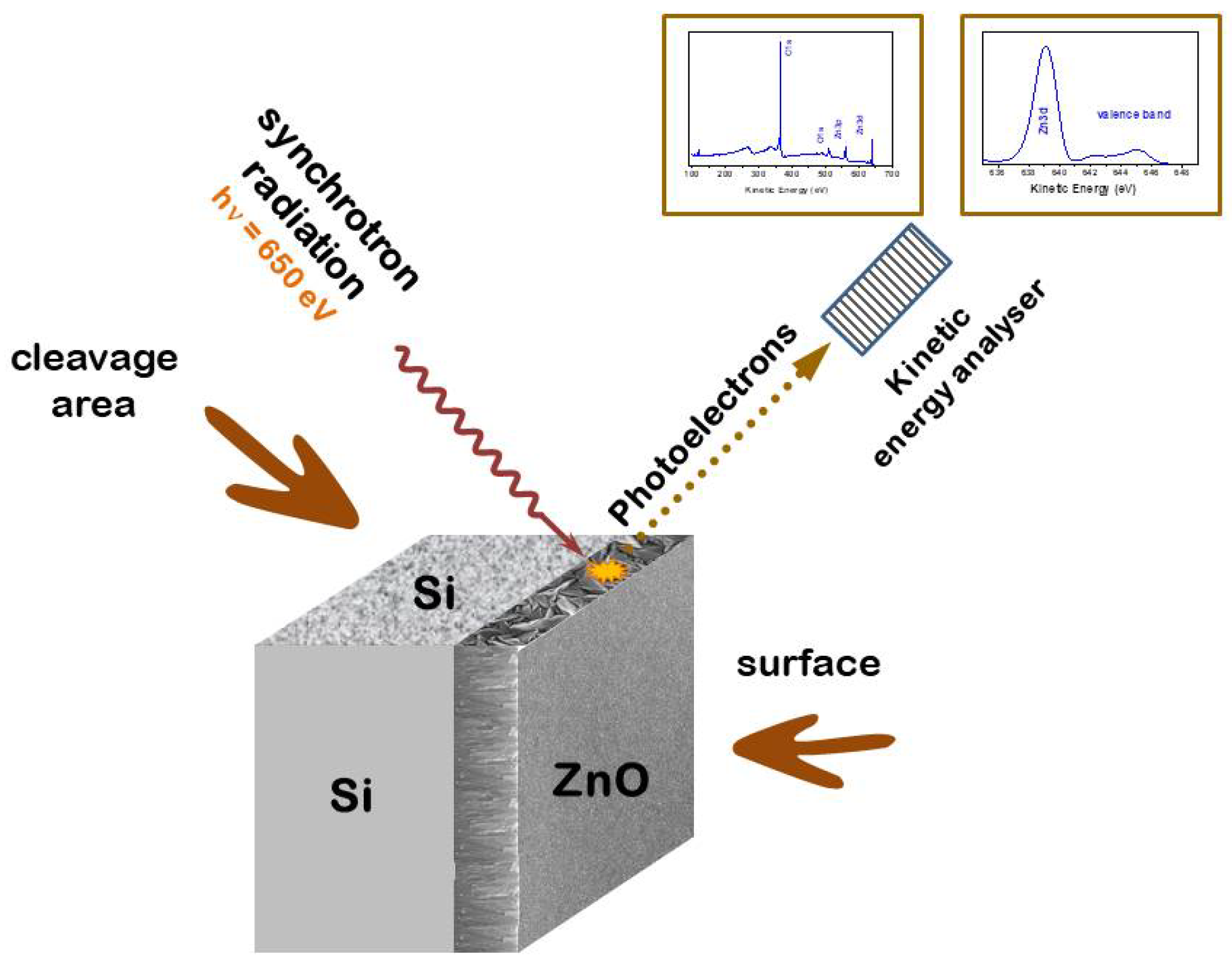
Figure 2.
(a) SPEM image of the cross-section of the ZnO:N film (6.4x3.2 um area) showing the points where photoemission spectra were taken, (b) photoemission spectra of the and the valence band region taken at points O, P, Q and R of the film cross-section, (c) the valence band region, (d) the edge of the valence band.
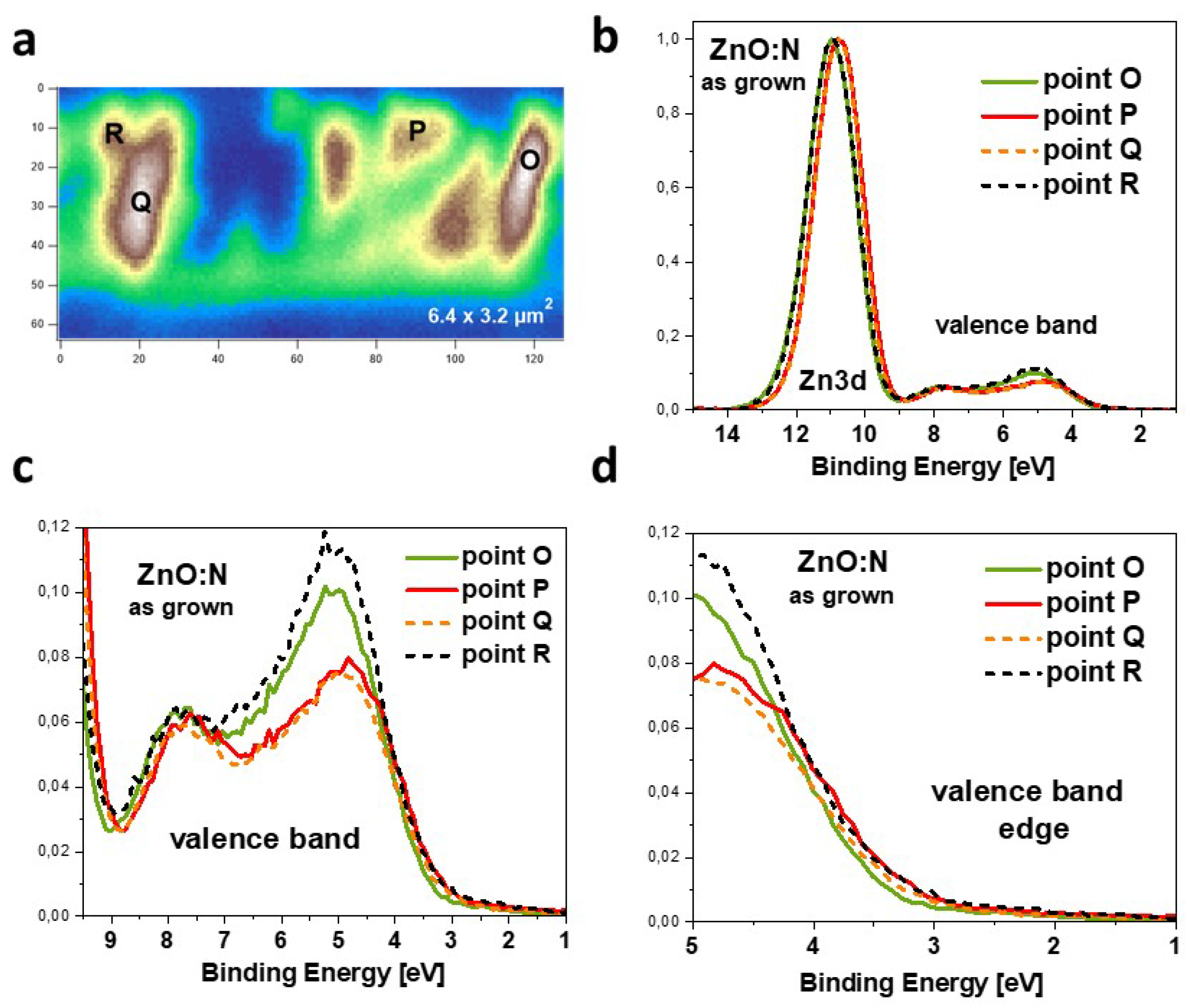
Figure 3.
(a) SPEM image of the cross-section of the annealed ZnO:N film (6.4x3,2 um area) showing the points where photoemission spectra were taken, (b) photoemission spectra of the and the valence band region taken at points C, D, F and G of the film cross-section, (c) the valence band region, (d) the edge of the valence band.
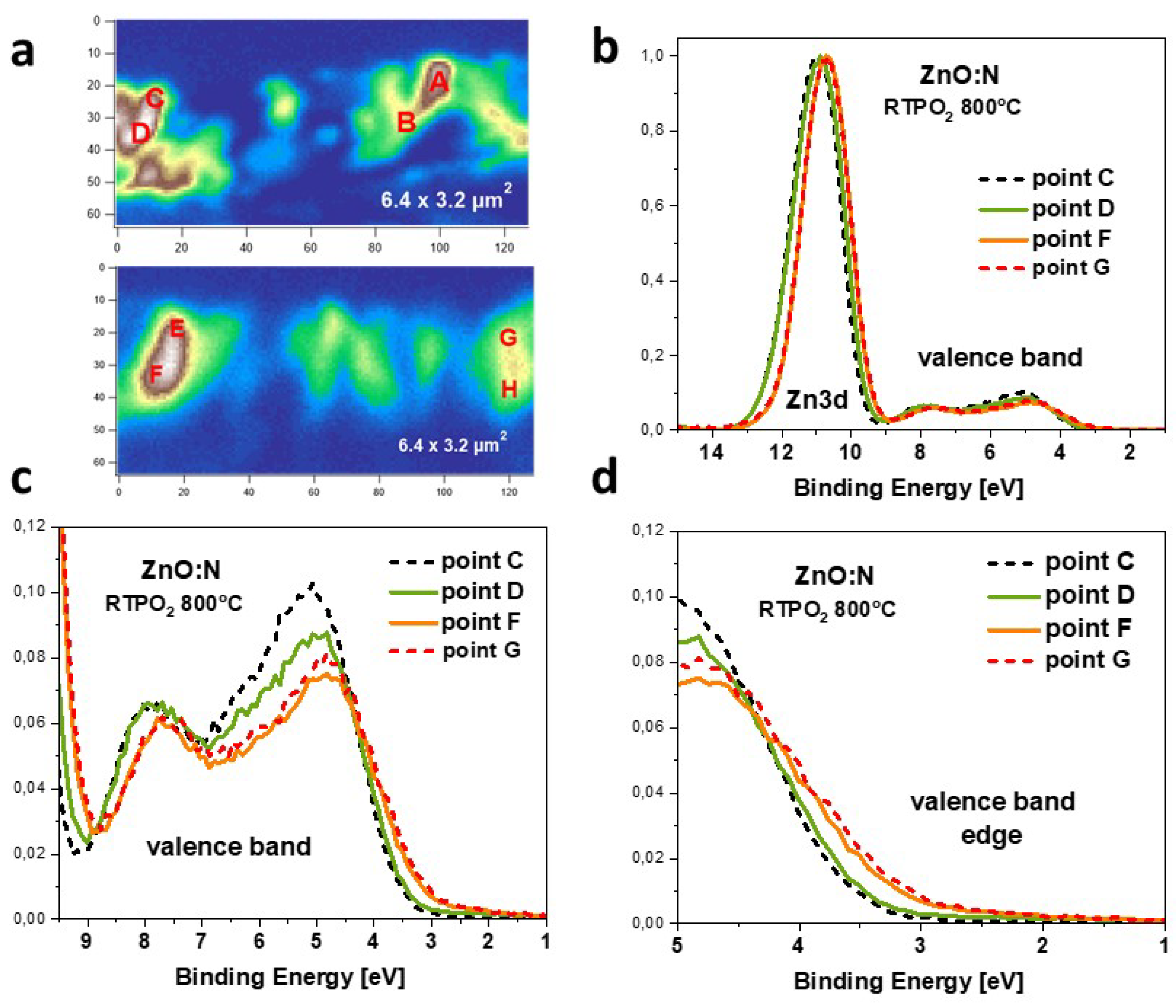
Figure 4.
Photoemission spectra of the core level in the ZnO:N/Si film measured at points O, P, Q and R of the film cross-section (points marked in Figure 2a).
Figure 4.
Photoemission spectra of the core level in the ZnO:N/Si film measured at points O, P, Q and R of the film cross-section (points marked in Figure 2a).
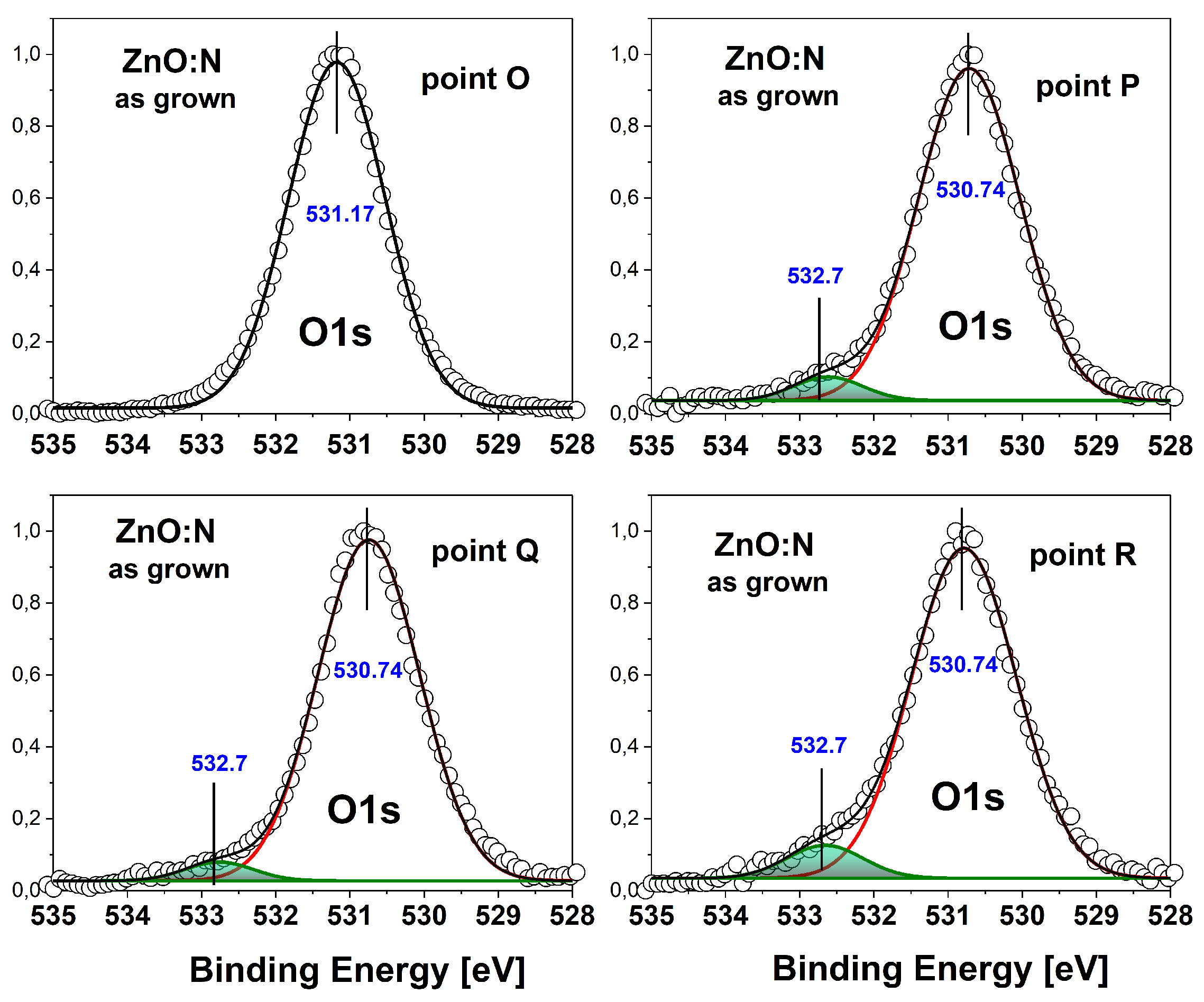
Figure 5.
Photoemission spectra of the core level in the annealed ZnO:N/Si film measured at points C, D, G and F of the film cross-section (points marked in Figure 3a).
Figure 5.
Photoemission spectra of the core level in the annealed ZnO:N/Si film measured at points C, D, G and F of the film cross-section (points marked in Figure 3a).
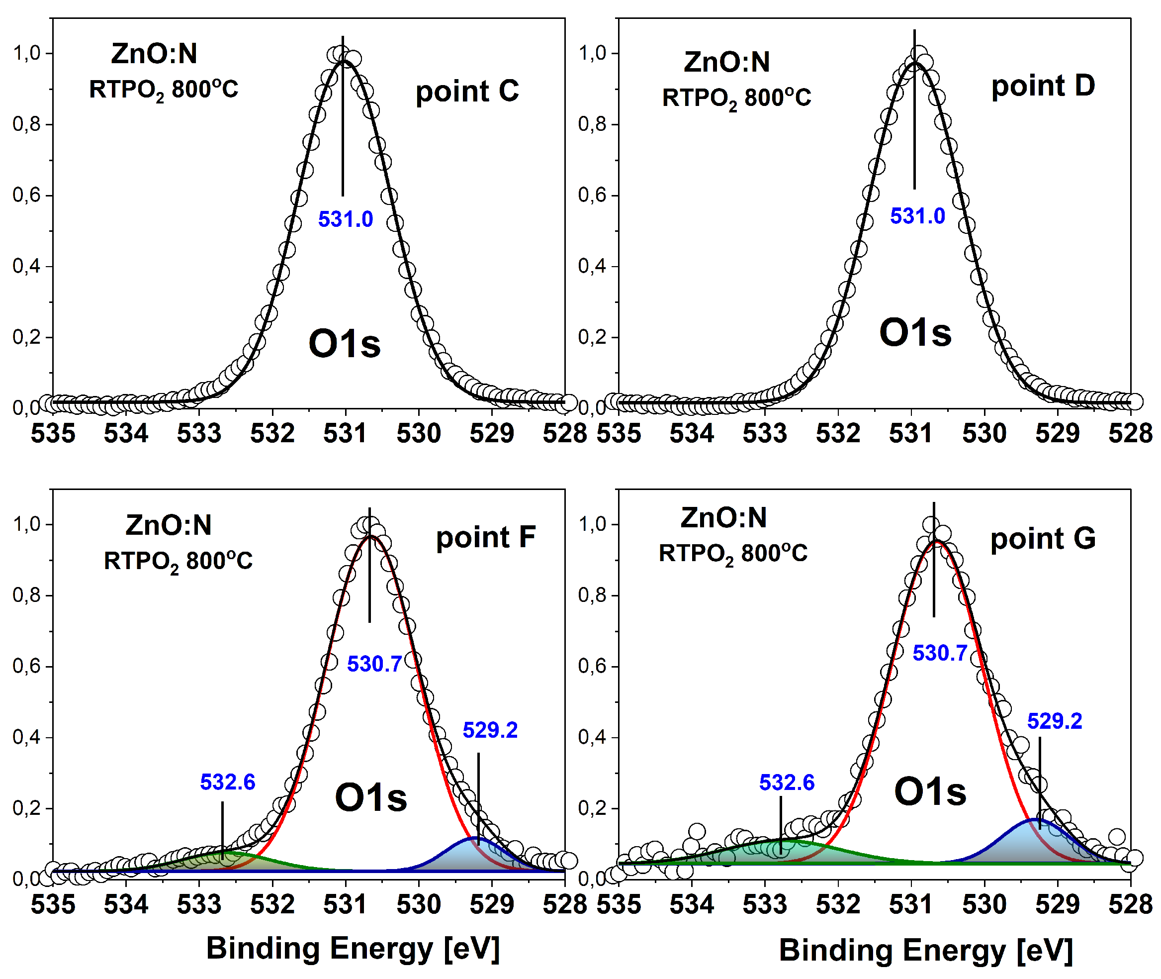
Figure 6.
Equilibrium atomic configurations of (a) Ci, (b) Ci-H, (c) Ci-H2 and (d) CiH–VZnNO complexes, respectively. The yellow isosurfaces (corresponded to 0.01 electron/Bohr3) represent the electronic wave-density distributions. The Zn atoms are drawn with large spheres (green), the O , N, and C atoms with medium spheres (red, blue and purple), and the H with small spheres (grey). The site of vacancy depicted by the black circle.
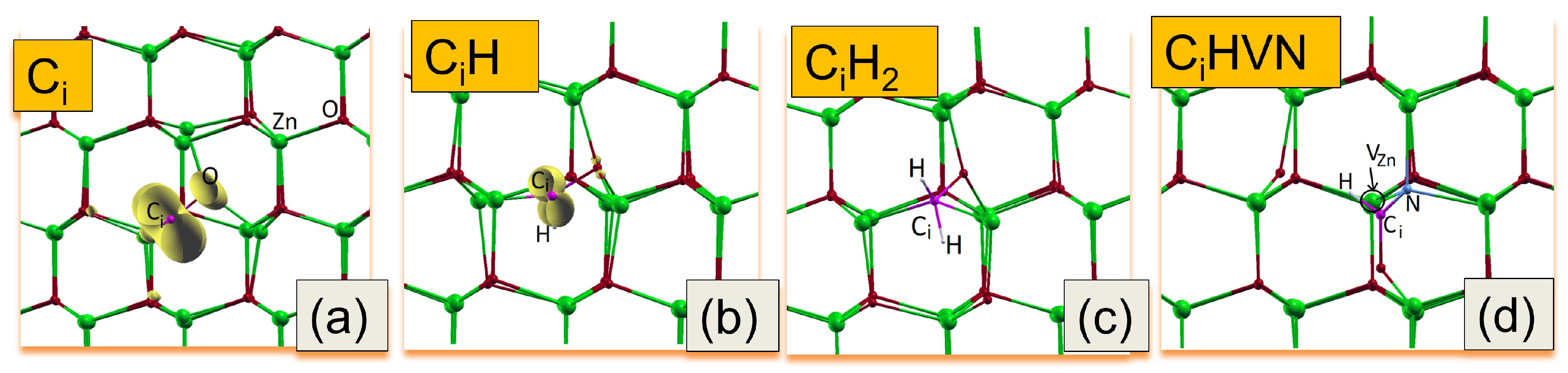
Figure 7.
(a–d) Diffusion paths of the VZn: (a), (b) in ZnO, without and with the presence of CH2 group, respectively. (c), (d) around the (NH)O complex in N:ZnO without and with the presence of CH2 group, respectively. (e–h) Atomic configurations of IS- or FS- states of VZn diffusion paths around (NH)O. The yellow isosurfaces (corresponded to 0.01 electron/Bohr3) represent the spin-density distributions for defect states. Complex is shown along c- axis. The site of vacancy depicted by the red circle and red arrows are depicted of the migration direction.
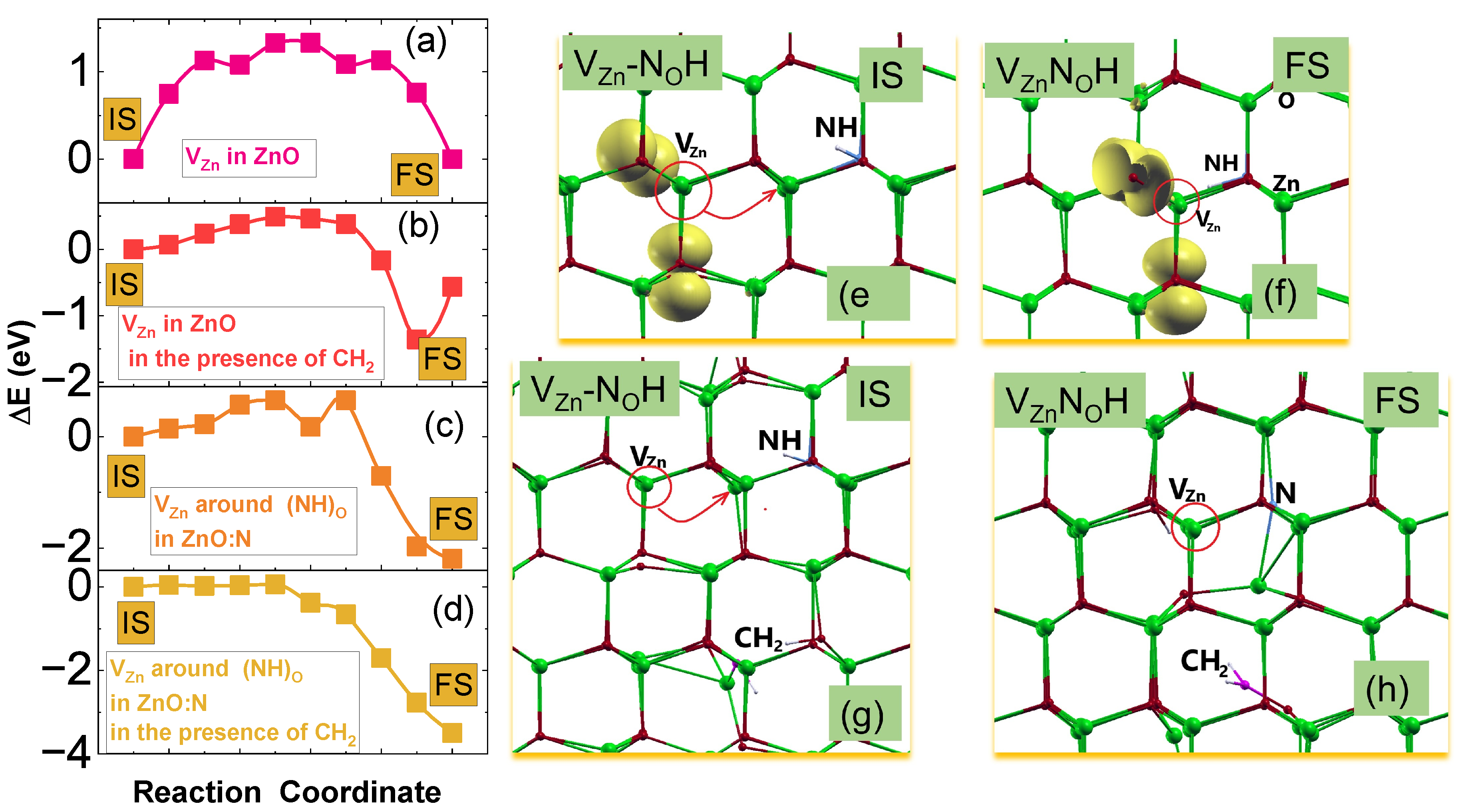
Figure 8.
Total density of states of undoped ZnO and ZnO including CH2 – and CH- VZnNO – complexes. Results shown with respect to the VBM of undoped ZnO.
Figure 8.
Total density of states of undoped ZnO and ZnO including CH2 – and CH- VZnNO – complexes. Results shown with respect to the VBM of undoped ZnO.
Disclaimer/Publisher’s Note: The statements, opinions and data contained in all publications are solely those of the individual author(s) and contributor(s) and not of MDPI and/or the editor(s). MDPI and/or the editor(s) disclaim responsibility for any injury to people or property resulting from any ideas, methods, instructions or products referred to in the content. |
© 2024 by the authors. Licensee MDPI, Basel, Switzerland. This article is an open access article distributed under the terms and conditions of the Creative Commons Attribution (CC BY) license (http://creativecommons.org/licenses/by/4.0/).
Copyright: This open access article is published under a Creative Commons CC BY 4.0 license, which permit the free download, distribution, and reuse, provided that the author and preprint are cited in any reuse.


