
Submitted:
02 December 2024
Posted:
03 December 2024
You are already at the latest version
Abstract
NiOx is a p-type semiconductor with excellent stability, which make it interesting for a wide range of applications. Broadband photodetectors with high responsivity (R) were fabricated by depositing r.f. sputtered NiOx layers on n-Si at room temperature (RT), 50 oC and 100 oC. In self-powered mode the RT diodes have R between 0.95 and 0.39 A/W for wavelengths between 365 and 635 nm, while at a reverse bias of -4V the responsivity increases to values between 22 A/W and 10.7 A/W for wavelengths in the same range. The increase of the deposition temperature leads to a decrease of R but also to a smaller reverse dark current. Thus, the 100 oC photodiodes might be more appropriate for applications where high responsivity is required, because of their smaller power consumption compared to the RT diodes. In addition, it was found that the increase of the deposition temperature leads to an increase of the diodes series resistance and the resistivity of NiOx. The effect of Rapid Thermal Annealing (RTA) on the properties of the photodiodes was studied. Annealing at 550 oC for 6 min leads to much higher responsivity compared to R of diodes with as-deposited NiOx. However, a disadvantage of the annealed diode is that the reverse current depends on the amplitude and polarity of previously applied bias voltage. The very high responsivity of the RTA photodiodes makes them useful as light sensors.
Keywords:
NiOx-nSi broadband photodetectors
; very high responsivity
; r.f. sputtering
; effect of RTA treatment
; light sensors
1. Introduction
NiOx is a p-type semiconductor with excellent chemical stability and high transmittance in the visible part of the electromagnetic spectrum [1]. Its bandgap varies between 3.4 and 4.3 eV depending on the deposition technique and conditions. Due to its electrical and optical properties NiOx is considered an attractive material for various applications, such as photovoltaic devices [2], electrochromic devices [3], gas sensors [4], ultraviolet and broadband photodetectors [5,6,7,8]. Various physical and chemical deposition techniques have been used to prepare NiOx films. Among the most commonly used methods are sputtering [9], sol-gel spin-coating [10,11,12], electron beam evaporation [7] and chemical vapor deposition [13]. The structural, optical and electrical properties of the NiOx layers depend strongly on the deposition technique. The magnetron r.f. sputtering is widely used because of the following advantages: high film quality, low density of defects, high adhesion, low cost and high deposition rate. NiOx films have been deposited by d.c. sputtering using metallic Ni in an Ar/O2 gas atmosphere. R.F. sputtering of NiO targets has also been studied. Despite recent advances, some challenges remain regarding the optimization of the optical and electrical properties of r.f. sputtered NiOx layers, especially for application in photodetectors. Variations of process parameters such as substrate temperature, deposition power, base and working pressures affect the deposited film characteristics.
Wang et al. reported the effect of varying the deposition temperature during reactive sputtering with a fixed r.f. power of 110 W [14]. Jamal et al. studied the effect of the variation of the growth temperature in the range between room temperature (RT) and 400 oC on the properties of r.f. sputtered NiO thin films, demonstrating that increasing the substrate temperature to 100°C results in suitable properties for photovoltaic applications [15]. Ahmed et al. reported the effect of r.f. power used in the deposition and showed that the best structural, morphological and optical properties of NiO were obtained at sputtering power of 200W [16]. Elmassi et al. investigated the variation of r.f. power on structural properties of NiO thin films obtained in an O2/Ar atmosphere, finding a relationship between power increment and crystallite size [17]. Abdur et al. investigated the impact of open-air post-annealing on the optoelectrical and structural properties of NiO films reporting that films deposited at 100°C showed favorable crystalline quality with the highest observed carrier mobility [18].
However, the results for the effect of the deposition temperature and thermal annealing processes on the properties of broadband photodetectors are limited. In this work, we study the properties of NiOx layers deposited by r.f sputtering from a NiO target at a fixed r.f. power of 60W and temperatures between RT and 100°C. In addition, the effect of post-deposition annealing of NiOx films on the optical and electrical properties Metal/NiOx/nSi heterojunction diodes was studied.
2. Results
Figure 1 (a) shows the experimental dependencies of the ellipsometric parameters Ψ and Δ and the fitted curves using the Cauchy dispersion model for a NiOx layer deposited at 100 oC and subjected to Rapid Thermal Annealing (RTA). Similar fitting results were obtained for the as-deposited layers prepared at RT, 50 oC and 100 oC and for the RTA layers deposited at the other two temperatures, RT and 50 oC. Figures 1 (b), (c) show the refractive index of the as-deposited and annealed NiOx films. From results in Figures 1 (b) and (c) it may be concluded that the RTA process does not lead to an important change of the optical constants. The layer thicknesses, deposition rate, the refractive index (n) and the extinction coefficient (k) at 632.8 nm of the as-deposited layers are shown in Table 1. The obtained values for the optical constants n and k are close to ones reported in the literature for NiOx [19].
Figure 2 (a) shows transmission spectra of a corning glass (CG) substrate and CG coated with NiOx layers deposited at RT, 50 oC and 100 oC. The transparency of CG was ≥80% in the range of 350–1000 nm. The transmittance of the sample with NiOx layer varies between ~60 and 80% in the visible – near IR range (400–1000 nm). Using the Tauc plot method the band gaps Eg of the films were obtained for the three deposition temperatures, 3.79, 3.82 and 3.91 eV, respectively (Figure 2 (b)). These results are in agreement with previously published values for Eg of NiO [7,19,20,21].
Figure 3 shows current-voltage (I-V) characteristics of photodiodes with NiOx layers deposited at RT, 50 oC and 100 oC measured by ramping the bias voltage in both directions. No hysteresis was observed in these measurements as well as after various consecutive measurements indicating low density of deep traps in the NiOx layer and in the NiOx/Si interfacial region. Typical rectifying dependences were measured with reverse saturation dark currents of ~3×10⁻⁷, 7×10⁻⁷ and 1×10⁻⁷ A for the three deposition temperatures. Under forward bias, the current increases exponentially to voltages of ~1 V for the RT diode and to ~0.7 V for the other two diodes, and then the characteristics change their shape because of the diodes series resistance. All diodes show photoresponse under reverse bias voltages (Vr < 0 V) and in self-powered mode (V = 0 V). The short circuit currents (ISC) under illumination with red, green, blue and UV light for the diodes with NiOx deposited at the three temperatures are given in Table 2. The open circuit voltage (VOC) depends slightly on the light intensity and varies between 0.2 V and 0.35 V depending on the light intensity and the NiOx deposition temperature (Figure 3 (a)-(c)). The photoresponse of the diodes with NiOx layer deposited at 100 oC is higher than that of the diodes obtained at 50 oC and is close to that of the diodes obtained at room temperature. However, an advantage of the 100 oC photodiodes is their smaller reverse dark current compared to the RT diodes.
I-V characteristics of diodes with NiOx layers deposited at the three temperatures and subjected to RTA process are shown in Figure 4. The thermal annealing leads to several important changes in the I-V dependences. Thus, the dark current and the photocurrents depend on the direction in which the bias voltage changes, leading to hysteresis at both, forward and reverse bias ramps. For forward biases, the current measured with bias increasing from 0 V towards positive voltages is smaller than the current measured in the opposite direction, most clearly seen in Figure 4 (b). The hysteresis is more pronounced under reverse biases and increases with the NiOx deposition temperature. The reverse bias voltages at which the current reaches saturation are close to or greater than -10 V (Figure 4 (a)-(c)). The photocurrents at these large negative voltages are greater than the photocurrents of the diodes with as-deposited NiOx layers. The highest values were obtained for the 50 oC, RTA diode (Figure 4 (b)). However, the I-V hysteresis of these photodiodes can be a disadvantage in their practical application. The inset in Figure 4 (b) shows a zoomed view of the current in the region of -0.5 – 0.5 V of a characteristic that was measured between 5 V and -10 V and then in the opposite direction. It can be seen that when ramping the bias from positive voltages towards 0 V the characteristic crosses the x-axis at positive voltage of 0.3 V, indicating increase of the negative charge trapped in the structure. In contrast, when the bias voltage varies from -10 V towards 0 V the characteristic crosses the x-axis at –0.3 V indicating increase of the positive trapped charge. Therefore, the observed hysteresis is more likely due to change of the charge state of shallow traps at the NiOx/n-Si heterojunction interface and in the interfacial region with the bias voltage. As a result, no open circuit voltage and short circuit current were measured. Since no shift was observed of the I-V curves of diodes with as-deposited NiOx layers it may be concluded that the RTA process has created defects, which can exchange carriers with Si, and as a result change their charge state.
Capacitance-Voltage (C-V) measurements were carried out in order to study in more details the effect of consecutive bias voltage ramps on the charge state of the diodes. The results in Figure 5 (a) show that ramping the voltage in both directions does not lead to hysteresis in the C-V curves of diodes with NiOx layers deposited at the three temperatures, indicating that no charge was trapped during these measurements. In contrast, the C-V characteristics of the diodes subjected to RTA when measured under reverse bias sweep from 0 V to -10 V and back to 0 V show a displacement of the C-V curves, corresponding to increase of the trapped positive charge in the diodes (Figure 5 (b)). In accordance with the I-V measurements the diodes with NiOx layer deposited at 50 oC showed the highest hysteresis.
3. Discussion
The series resistance (Rs) reduces the voltage applied on the heterojunction and thus affects the I-V characteristic. Rs can be evaluated from the slope of the If/g vs. If characteristic [22], where If is the forward current in the region after the exponential increase of I and g is the conductance dIf/dVf. In this region Rs leads to change of the shape of the I-V curve. The dependence of I/g on I may be derived by differentiating the I-V equation
where n is the ideality factor, which gives
or
By simple algebraic transformations a linear dependence of I/g on the forward current I is obtained
Figure 6 (a) displays the I/g vs. I dependencies for no annealed diodes with NiOx layers deposited at RT, 50 oC and 100 oC. The slope of the straight lines increases with the deposition temperature, indicating that Rs also increases. Since the resistivity of the n-type region of the heterojunction, n-Si, is constant it may be concluded that the increase of the deposition temperature leads to an increase of the resistivity of the NiOx layers. Similar effect of increased resistivity was observed at a constant deposition temperature with increase of the r.f. power [23,24].
The dependence of the forward current on the voltage sweep direction makes it impossible to evaluate the series resistances of the diodes after RTA. An approximate estimation was obtained for the RTA diode with NiOx layer deposited at RT (Figure 4 (a)) by using the I-V characteristic measured from 0 V towards positive voltages. The obtained result is compared with the I/g vs. I dependence for a no annealed diode with NiOx layer deposited at 100 oC, the one with the highest Rs (Figure 6 (b)). The line slopes in Figure 6 (b) indicate that the RTA process leads to comparable or even higher values of Rs than those of the 100 oC diodes.
The responsivity (R) of the fabricated photodiodes was calculated from [25]
where Iph = Ilight – Idark is the photocurrent, Pλ is the incident optical power at a specific wavelength λ and A is the area of the top contact. High responsivity was determined for the no annealed photodiodes. The results are shown in Figure 7 (a) and in Table 3. The responsivity of the diodes with NiOx layer deposited at RT is higher than R of the other diodes in self-powered mode, as well as at reverse bias of -4 V. For applications where self-biased mode of operation is required, the RT diodes are the most appropriate. However, for some applications where higher responsivity is required the 100 oC photodiodes may be better option because of their smaller dark current at -4 V and R, which is close to that of the RT diode. The responsivity of the diodes subjected to RTA under Vr = -10 V is shown in Figure 7 (b). Very high values for R were determined under bias voltage of -10 V, much higher than the ones reported in the literature for broadband photodetectors. While the R of the RTA, 50 oC diode is the highest one this diode can be less appropriate because of it’s higher dark current and lack of saturation of the photocurrent even at reverse bias voltage of -10 V. Although the RTA annealed diodes may not be appropriate for applications where precise measurement of the optical power is required, they may be useful as light sensors because of their high responsivity.
The obtained results for R at 0 V and at -4 V for photodiodes with as-deposited NiOx layers are compared with results reported in the literature in Table 4. The determined responsivity of the photodiodes deposited at RT and 100°C are among the highest reported and are comparable with results published by other authors. Ma et. al. reported a responsivity of 15.8 A/W at -5V, which is slightly higher than our result for 100 oC diodes, however the maximum bias voltage used here was -4V.
Another relevant parameter is the specific detectivity (D*), which can be defined as the sensibility of a photodiode to detect weak light signals. D* involves the R at a given wavelength of the excitation light, the elementary charge (q) and the dark current density (JD) and is given by
The values obtained for the detectivity are close to the best values reported in the literature for NiOx based photodetectors (Table 4).
4. Materials and Methods
NiOx thin films were deposited on n-type (100) Si wafers with resistivity of 4–10 Ωꞏcm by R.F. magnetron sputtering at 25 oC (RT), 50 oC and 100 oC. The deposition time was 6 min for the three temperatures. Prior to deposition, the substrates were cleaned in an ultrasonic bath for 5 minutes with acetone, isopropyl alcohol and deionized water and dried with high-purity nitrogen. NiO target (99.9%) with dimensions of 50.8 × 3.175 mm at a working distance of 7 cm was used for deposition. The sputtering gas was ultra-high-purity (UHP) argon (99.9999%). The chamber base pressure was 1×10⁻⁵ Torr, the working pressure was 5 mTorr and the Ar flow was 18.9 sccm. Before the deposition the target was pre-sputtered for 20 minutes. To study the effect of thermal annealing, half of the samples were subjected to RTA process in an UHP N2 atmosphere. The annealing was performed in a horizontal tube furnace (Zhengzhou CY Scientific Instrument Co.) equipped with a sliding rail. The N2 flow rate was maintained at 100 mL/min, and the samples were annealed at 550 °C for 6 minutes. Following the annealing process, the samples were allowed to cool to room temperature under the same N2 environment to ensure controlled conditions. For electrical characterization semitransparent Au electrodes (~50 nm of thickness) with area of 95 × 95 μm2 spaced by 30 μm, were thermally evaporated through a shadow mask as top contacts. Aluminum with a thickness of ~300 nm was used as back contact.
The thickness and the optical constants, refractive index and extinction coefficient, were determined by ellipsometric measurements using Variable Angle Spectroscopic Ellipsometer J.A. Woollam M – 2000U. The measurements were carried out at three angles of incidence in the range of 50° - 70°. The experimental results for the ellipsometric angles Ψ and Δ were fitted in the 400 – 1000 nm range using the Cauchy dispersion model. Electrical characterization was carried out by Keithley 4200-SCS Semiconductor Characterization System. I-V dependencies were measured in dark and under illumination with red, green, blue and UV light emitting diodes (LEDs). The LEDs optical powers are given in Table 5. C-V characteristics were measured in dark at frequency of 100 kHz using a test signal with amplitude of 30 mV. The bias sweep delay time and hold time for the I-V and C-V measurements were 0.5 s and 1 s, respectively, while the voltage steps used were 50 or 100 mV.
5. Conclusions
Photodetectors with high responsivity in self-powered mode and at reverse bias of -4 V were fabricated by depositing r.f. sputtered NiOx layers on n-Si at RT, 50 oC and 100 oC. The increase of the deposition temperature leads to a decrease of R at V = 0 V and Vr = -4 V but also to a smaller dark current at reverse biases. In addition, higher deposition temperature leads to an increase of the diodes series resistance and of the NiOx resistivity. The diodes fabricated after RTA annealing show much higher R compared to those with as-deposited layers. A disadvantage of these diodes is the dependence of their dark current and photocurrents on the direction of the bias voltage change. As a result, the annealed diodes may be inappropriate for applications where exact determination of the optical power is required but because of the very high responsivity, they might be useful as light sensors.
References
- Napari, M.; Huq, T.N.; Hoye, R.L.Z.; MacManus-Driscoll, J.L. Nickel oxide thin films grown by chemical deposition techniques: potential and challenges in next-generation rigid and flexible device applications. InfoMat 2021, 3, 536–576. [CrossRef]
- Aivalioti, C.; Manidakis, E.G.; Pelekanos, N.T.; Androulidaki, M.; Tsagaraki, K.; Viskadourakis, Z.; Spanakis, E.; Aperathitis, E. Niobium-doped NiO as p-type nanostructured layer for transparent photovoltaics. Thin Solid Films 2023 778 139910. [CrossRef]
- Wang, F.; Zhang, W.; Jia, J.; Chen, Y.; Chen, Z.; Wang, Z.; Zhang, L.; Ma, H. Improvement of electrochromic properties of NiO film doped with ZnO prepared by magnetron sputtering. J. Mater. Sci. Mater. Electron 2024, 35,455. [CrossRef]
- Li, C.; Choi, P.G.; Kim, K.; Masuda, Y. High performance acetone gas sensor based on ultrathin porous NiO nanosheet. Sens. Actuat. B-Chem 2022,367,132143. [CrossRef]
- Peng, Y.; Jiang, D.; Zhao, M.; Duan, Y.; Wei, H.; Li, H.; Liang, Q.; Wang, S. High-performance UV–visible photodetectors based on ZnO/perovskite heterostructures. J. Alloys Compd. 2023, 965,171372. [CrossRef]
- Chen, L.; Wang, Y.; Zhang, J.; Chen, L.; Zhai, J.; Song, J. Inorganic Semiconductor-Based Flexible UV Photodetector Arrays Achieved by Specific Flip-Chip Bonding. ACS Appl. Mater. Interfaces 2024, 16, 51089–51096. [CrossRef]
- Castillo-Saenz, J.R.; Nedev, N.; Valdez-Salas, B.; Bernechea, M.; Martínez-Guerra, E.; Mendivil-Palma, I.; Curiel-Alvarez, M.; Mateos, D.; Perez-Landeros, O. Effect of oxidation temperature on the properties of NiOx layers for application in optical sensors. Thin Solid Films 2021, 734, 138849. [CrossRef]
- Ahmed, A.A.; Hashim, M.R.; Qahtan, T.F.; Rashid, M. Preparation and characteristics study of self-powered and fast response p-NiO/n-Si heterojunction photodetector. Ceram. Int. 2022, 48, 20078–20089.
- Wang, J.; Li, Q.; Mi, W.; Wang, D.; Xu, M.; Xiao, L.; Zhang, X.; Luan, C.; Zhao, J. Fast response self-powered solar-blind UV photodetector based on NiO/Ga2O3 p-n junction. Mater. Sci. Semicond. Process. 2025, 186, 109084. [CrossRef]
- Hwang, J.-D.; Cheng, Y.-A. Enhancing the Performance of NiO-Based Metal-Semiconductor-Metal Ultraviolet Photodetectors Using a MgO Capping Layer. IEEE Sens. J. 2021, 21, 27400–27404.
- Caglar, M.; Sever, K.; Aktas, S.; Demiroglu A. Improving the electrical performance of NiO based photodiode fabricated by sol-gel process with Al doping. Sensor Actuat A-Phys 2023, 350, 114099. [CrossRef]
- Pandit, B.; Parida,B., Jang H-S;Heo K. Self-Powered Broadband Photodetector Based on NiO/Si Heterojunction Incorporating Graphene Transparent Conducting Layer. Nanomaterials 2024, 14, 551 1-11.
- Wilson, R.L.; Macdonald, T.J.; Lin, C.-T.; Xu, S.; Taylor, A.; Knapp, C.E.; Guldin, S.; McLachlan, M.A.; Carmalt, C.J.; Blackman, C.S. Chemical vapour deposition (CVD) of nickel oxide using the novel nickel dialkylaminoalkoxide precursor [Ni(dmamp′)2] (dmamp′ = 2-dimethylamino-2-methyl-1-propanolate). RSC Adv 2021, 11, 22199–22205. [CrossRef]
- Wang, H.; Zhao, Y.; Li, X.; Zhen, Z.; Li, H.; Wang, J.; Tang, M. Effect of Sputtering Temperature on Structure and Optical Properties of NiO Films Fabricated by Magnetron Sputtering. J. Electron. Mater 2017, 46, 4052–4056. [CrossRef]
- Jamal, M.S.; Shahahmadi, S.A.; Chelvanathan, P.; Alharbi, H.F.; Karim, M.R.; Dar, M.A.; Luqman, M.; Alharthi, N.H.; Al-Harthi, Y.S.; Aminuzzaman, M.; Asim, N.; Sopian, K.; Tiong, S.K.; Amin, N.; Akhtaruzzaman, Md. Effects of growth temperature on the photovoltaic properties of RF sputtered undoped NiO thin films. Results Phys 2019, 14, 102360. [CrossRef]
- Ahmed, A.A.; Hashim, M.R.; Rashid, M. Effect of RF power on structural, morphological and optical properties of NiO thin films. In Proceedings of AIP Conference, Kelantan, Malaysia, 6 February 2019.
- Elmassi, S.; Narjis, A.; Nkhaili, L.; Elkissani, E.; Amiri, L.; Drissi, S.; Abali, A.; Bousseta, M.; Outzourhit, A. Effect of annealing on structural, optical and electrical properties of nickel oxide thin films synthesized by the reactive radio frequency sputtering. Phys. B Condens. Matter 2022, 639, 413980. [CrossRef]
- Abdur, R.; Choudhury, S.; Bashar, M.S.; Hossain, M.R.; Quddus, M.S.; Akhtar, U.S.; Shaikh, M.A.A; Hossain, M. Enhancing perovskite solar cell performance: Investigating the impact of post-annealing on the optoelectrical and structural properties of RF-sputtered NiO films via SCAPS-1D device modeling. Sol. Energy 2024, 271, 112443. [CrossRef]
- Koushik, D.; Josˇt, M.; Ducˇinskas, A.; Burgess, C.; Zardetto, V.; Weijtens, C.; Verheijen, M.A.; Kessels, W.M.M.; Albrecht, S.; Creatore, M. Plasma-assisted atomic layer deposition of nickel oxide as hole transport layer for hybrid perovskite solar cells. J. Mater. Chem C 2019, 7, 12532 –12543. [CrossRef]
- Abzieher, T.; Moghadamzadeh, S.; Schackmar, F.; Eggers, H.; Sutterlüti, F.; Farooq, A.; Kojda, D.; Habicht, K.; Schmager, R.; Mertens, A.; Azmi, R.; Klohr, L.; Schwenzer, J.A.; Hetterich, M.; Lemmer, U.; Richards, B.S.; Powalla, M.; Paetzold, U.W. Electronbeam-evaporated nickel oxide hole transport layers for perovskite-based photovoltaics. Adv. Energy Mater 2019, 9, 1802995.
- Hasan, M.R.; Xie, T.; Barron, S.C.; Liu, G.; Nguyen, N.V.; Motayed, A.; Rao, M.V.; Debnath, R. Self-powered p-NiO/n-ZnO heterojunction ultraviolet photodetectors fabricated on plastic substrates. Apl. Mater 2015, 3, 10610.
- Schroder, D.K. Semiconductor material and device characterization, 3rd ed.; Publisher: John Wiley & Sons New Jersey, USA, 2006; p. 187. [CrossRef]
- Grilli, M.L.; Aydogan, S.; Yilmaz, M. A study on non-stoichiometric p-NiOx/n-Si heterojunction diode fabricated by RF sputtering: determination of diode parameters. Superlattice. Microst 2016, 100, 924–933.
- Mateos-Anzaldo, D.; Nedev, R.; Perez-Landeros, O.; Curiel-Alvarez, M.; Castillo-Saenz, J.; Arias-Leon, A.; Valdez-Salas, B.; Silva-Vidaurri, L.; Martinez-Guerra, E.; Osorio-Urquizo, E.; Nedev, N. High-performance broadband photodetectors based on sputtered NiOx/n-Si heterojunction diodes. Optical Materials 2023, 145, 114422.
- Chen, X.; Ren, F.; Gu, S.; Ye, J. Review of gallium-oxide-based solar-blind ultraviolet photodetectors, Photon. Res. 2019, 7, 381 –415. [CrossRef]
- Hammadi, O. A.; Khalaf, M. K.; Kadhim, F. J. Fabrication of UV Photodetector from Nickel Oxide Nanoparticles Deposited on Silicon Substrate by Closed-Field Unbalanced Dual Magnetron Sputtering Techniques. Optical and Quantum Electronics 2015, 47 (12), 3805–3813. [CrossRef]
- Ahmed, A. A.; Hashim, M. R.; Qahtan, T. F.; Rashid, M. Multi – Wavelength Photodetectors Based on Porous Spin-Coated and Compact RF-Sputtered NiO Films Grown over Si Substrate: Effect of Surface Morphology. Optik 2022, 255, 168694–168694. [CrossRef]
- Xu, J.; Cao, R.; Shi, S.; Li, L.; Zhu, K.; Su, Y. Self-Powered Ultraviolet Photodetectors Based on Match like Quasi One-Dimensional N-TiO2/P-NiO Core-Shell Heterojunction Arrays with NiO Layer Sputtered at Different Power. Journal of Alloys and Compounds 2022, 928, 167126.
- Enns, Y.; Sergei Timoshnev; Alexey Kazakin; Ksenia Shubina; Uvarov, A.; Vorobyev, A.; Ekaterina Nikitina; Andrey Mizerov; Andreeva, V.; Fedorenko, E.; Koroleva, A.; Evgeniy Zhizhin. Characterization of the P-NiO/N-GaN Heterojunction and Development of Ultraviolet Photodiode. Materials Science in Semiconductor Processing 2024, 181, 108624–108624.
- Ma, X.; Tang, L.; Jia, M.; Zhang, Y.; Zuo, W.; Cai, Y.; Li, R.; Yang, L.; Teng, K. S. Ultrahigh Performance UV Photodetector by Inserting an al2O3 Nanolayer in NiO/N-Si. Advanced Electronic Materials 2024, 10 (9).
Figure 1.
(a) Experimental Ψ and Δ dependences and the fitted curves for a layer deposited at 100 oC and subjected to RTA. Refractive index for: (b) As-deposited layers; (c) RTA annealed layers.
Figure 1.
(a) Experimental Ψ and Δ dependences and the fitted curves for a layer deposited at 100 oC and subjected to RTA. Refractive index for: (b) As-deposited layers; (c) RTA annealed layers.
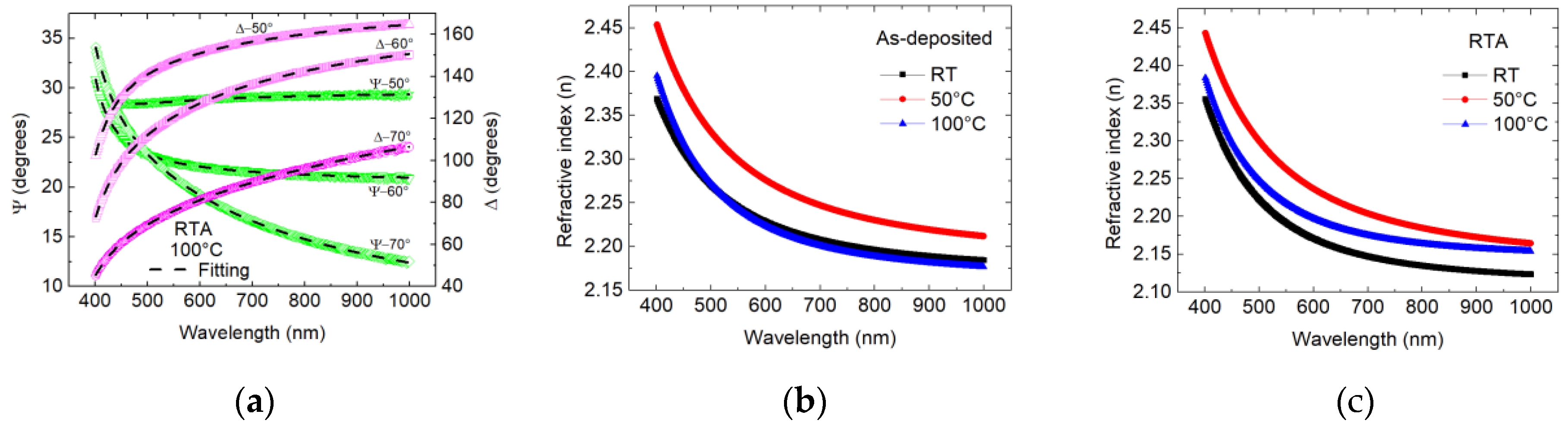
Figure 2.
(a) Transmittance of CG substrate and CG coated with NiOx layers deposited at RT, 50 oC and 100 oC; (b) Band gaps of the films determined by the Tauc plot method.
Figure 2.
(a) Transmittance of CG substrate and CG coated with NiOx layers deposited at RT, 50 oC and 100 oC; (b) Band gaps of the films determined by the Tauc plot method.
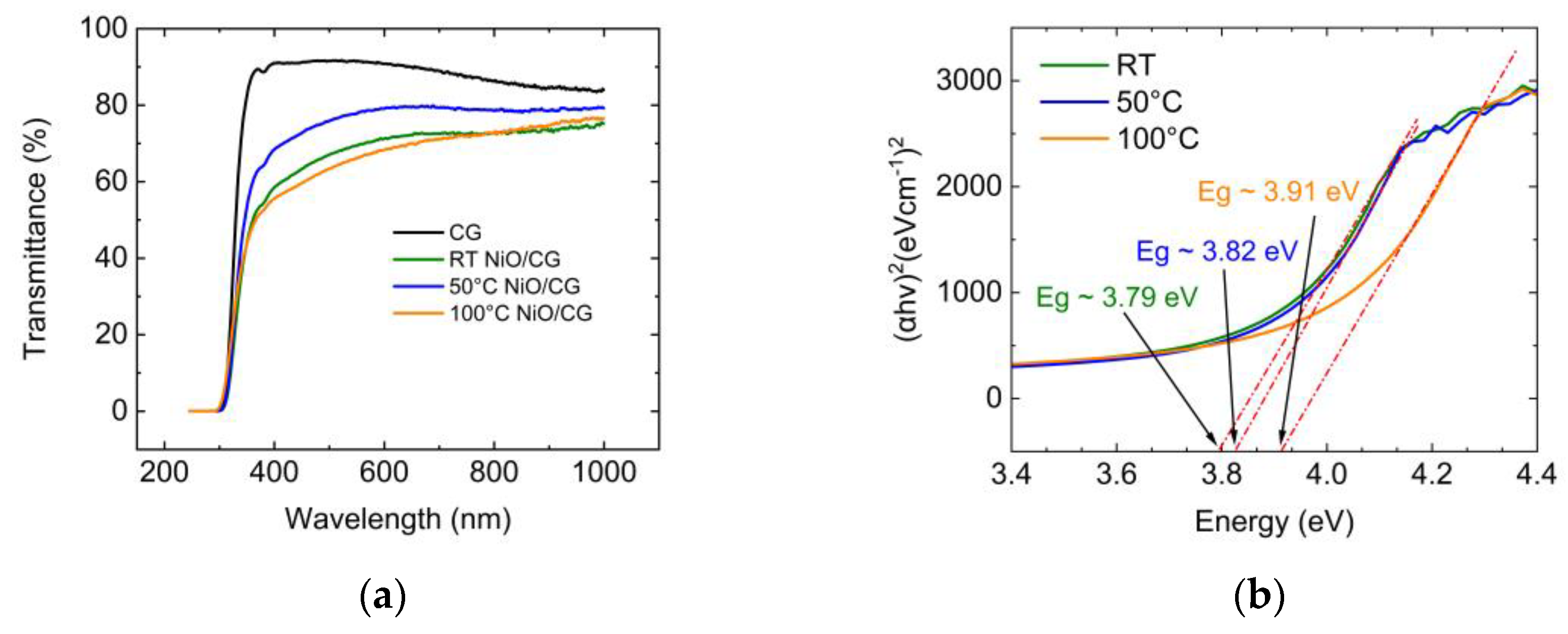
Figure 3.
I-V characteristics of photodiodes with NiOx layers deposited at: (a) RT, (b) 50 oC and (c) 100 oC measured in dark and under illumination with red, green, blue and UV light.
Figure 3.
I-V characteristics of photodiodes with NiOx layers deposited at: (a) RT, (b) 50 oC and (c) 100 oC measured in dark and under illumination with red, green, blue and UV light.
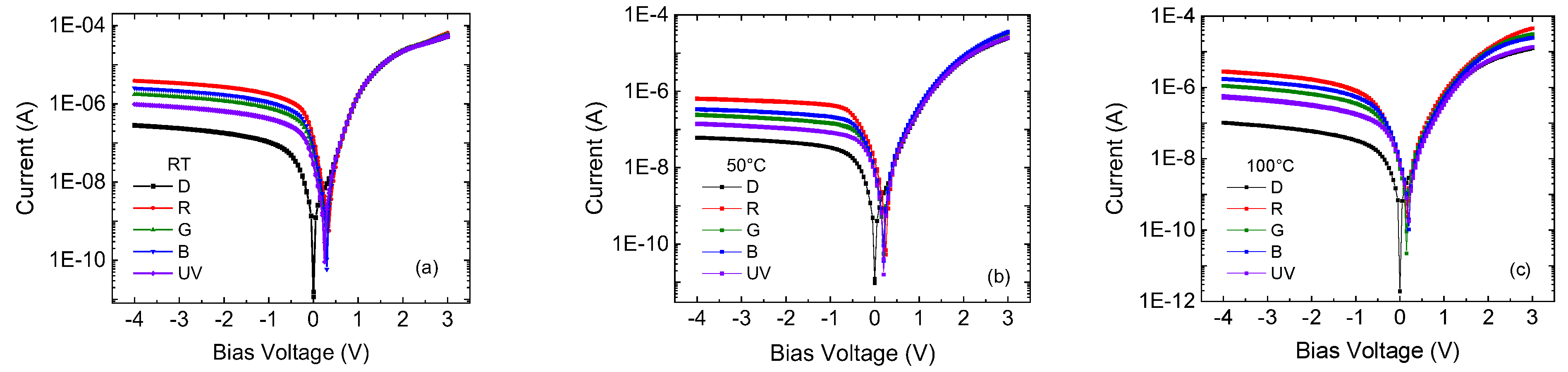
Figure 4.
I-V characteristics of photodiodes with NiOx layers deposited at: (a) RT, (b) 50 oC and (c) 100 oC and subjected to RTA annealing. The dependences were measured in dark and under illumination with red, green, blue and UV light.
Figure 4.
I-V characteristics of photodiodes with NiOx layers deposited at: (a) RT, (b) 50 oC and (c) 100 oC and subjected to RTA annealing. The dependences were measured in dark and under illumination with red, green, blue and UV light.
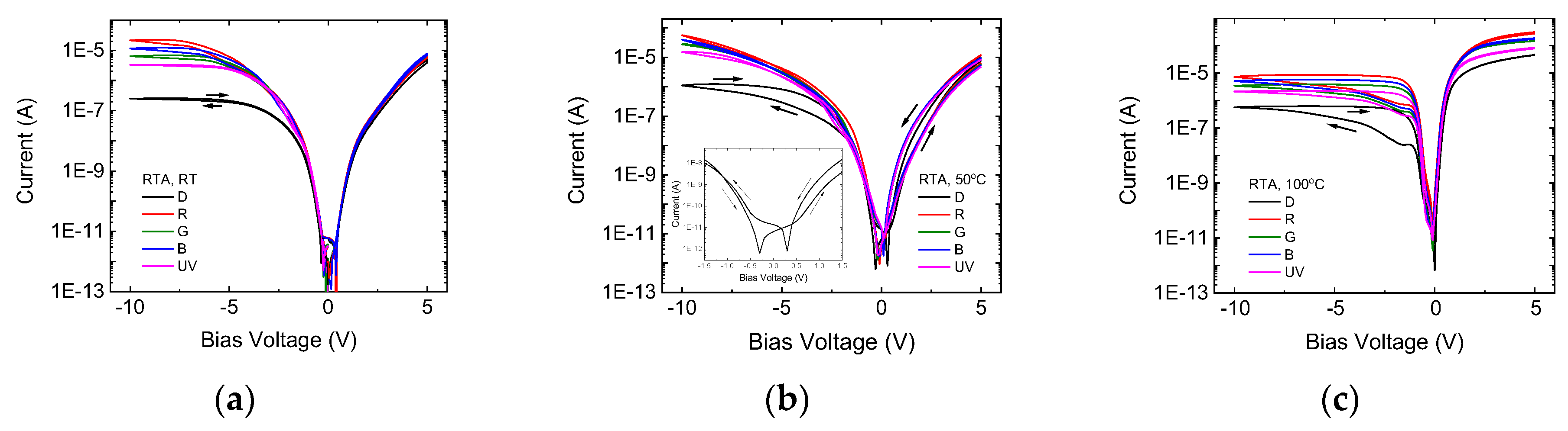
Figure 5.
C-V characteristics measured under reverse bias of: (a) Diodes with as-deposited NiOx layers; (b) Diodes with RTA annealed layers.
Figure 5.
C-V characteristics measured under reverse bias of: (a) Diodes with as-deposited NiOx layers; (b) Diodes with RTA annealed layers.
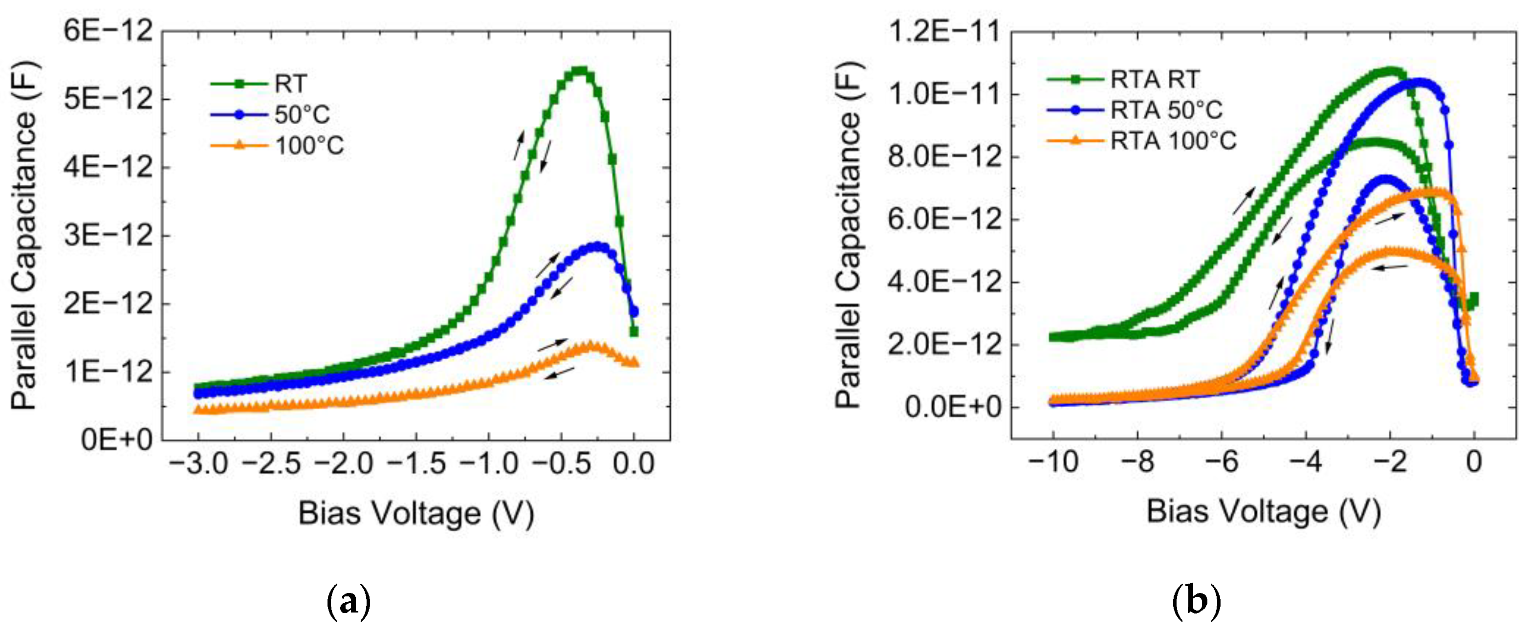
Figure 6.
(a) I/g vs. I dependencies for diodes with as-deposited NiOx layers prepared at RT, 50 oC and 100 oC. Higher line slope corresponds to higher Rs; (b) Comparison of the I/g vs. I dependences for a diodes with as-deposited NiOx prepared at 100 oC (red line) and a RTA annealed diode with NiOx layer deposited at RT (black line); Note the difference in x-axis scale.
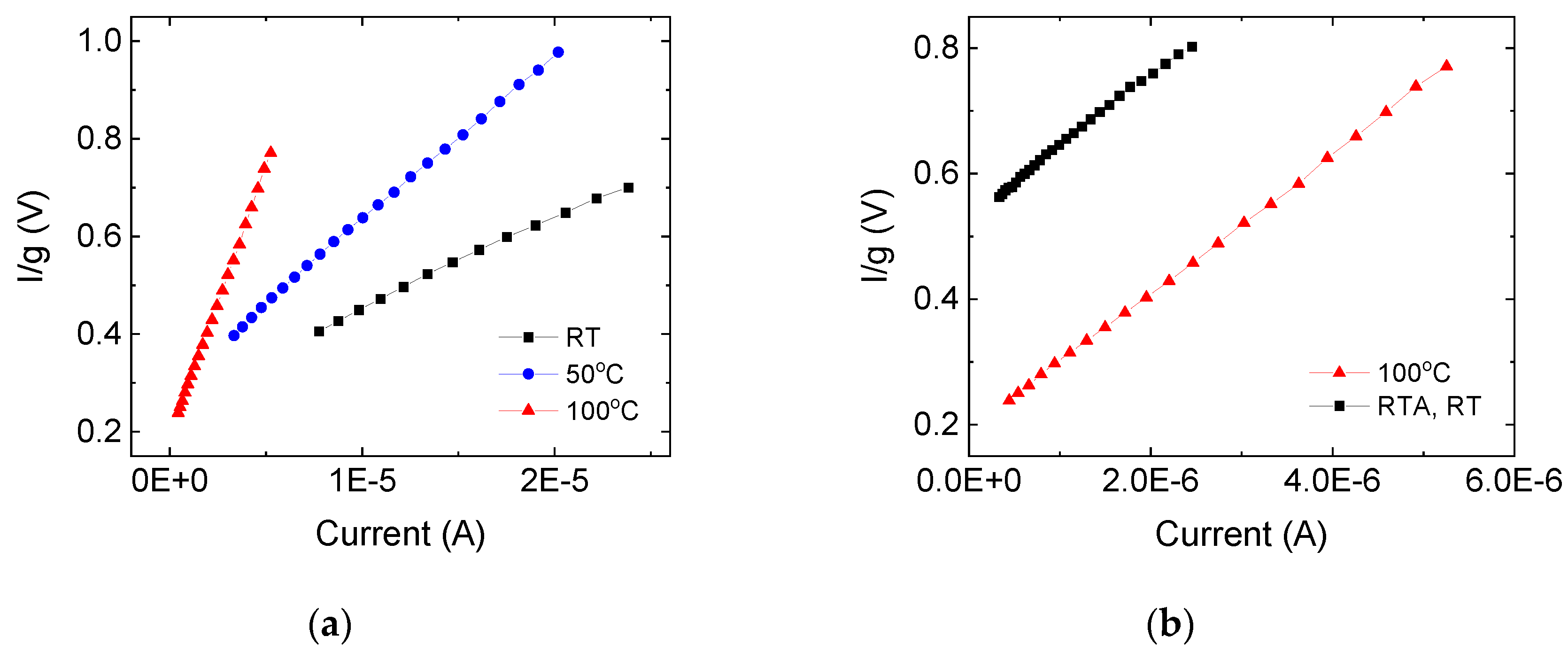
Figure 7.
Responsivity of photodiodes with: (a) As-deposited NiOx layers; (b) RTA annealed NiOx layers.
Figure 7.
Responsivity of photodiodes with: (a) As-deposited NiOx layers; (b) RTA annealed NiOx layers.
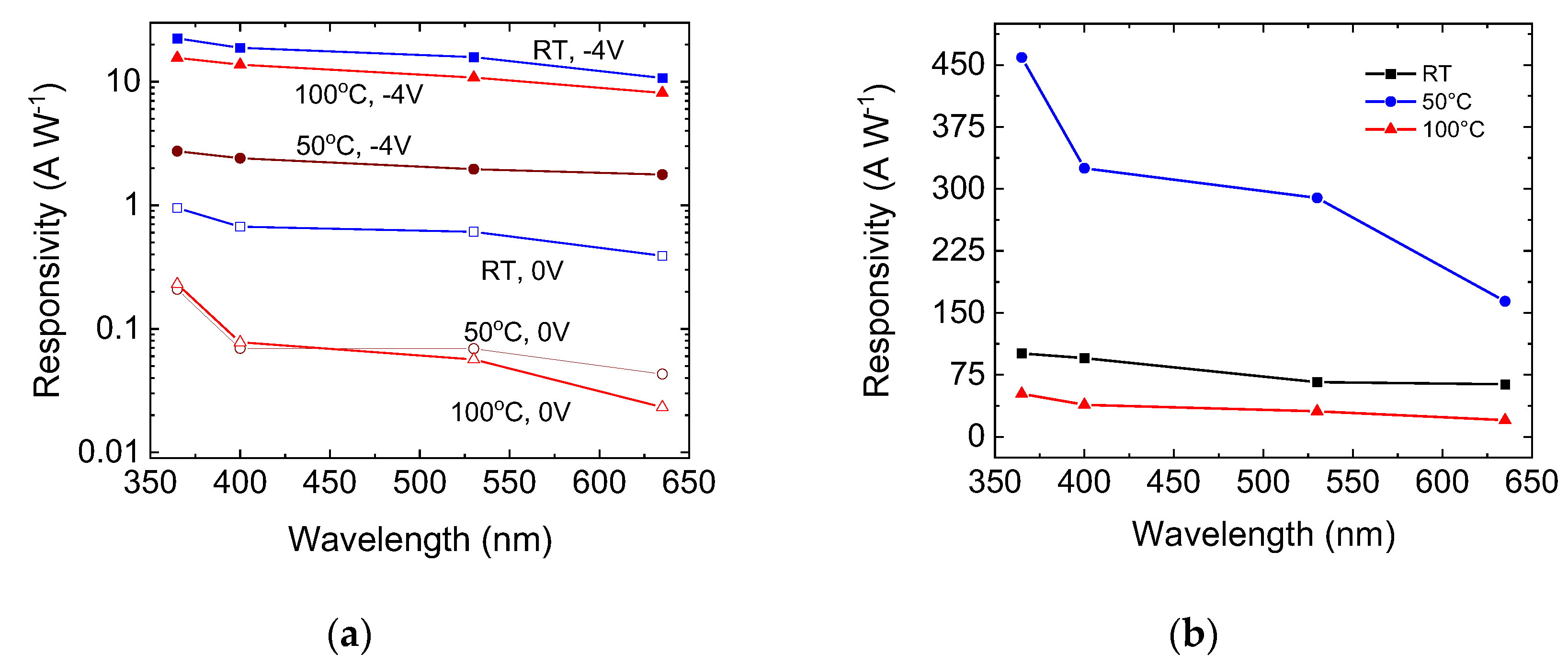

Table 1.
Thickness, deposition rate and optical constants n and k at 632.8 nm for layers deposited at the three temperatures.
Table 1.
Thickness, deposition rate and optical constants n and k at 632.8 nm for layers deposited at the three temperatures.
| Temperature (oC) | Thickness (nm) | Deposition rate (nm/min) | n | k |
|---|---|---|---|---|
| Room Temperature | 41.5 | 6.92 | 2.25 | 0.03 |
| 50 | 48.9 | 8.15 | 2.29 | 0.044 |
| 100 | 36 | 6 | 2.25 | 0.01 |
Table 2.
Short circuit currents under illumination with red, green, blue and UV light for the diodes with NiOx deposited at the three temperatures.
Table 2.
Short circuit currents under illumination with red, green, blue and UV light for the diodes with NiOx deposited at the three temperatures.
| Light color | ISC (A) | ||
|---|---|---|---|
| RT | 50 oC | 100 oC | |
| Red | 1.30E-07 | 1.50E-08 | 7.85E-09 |
| Green | 5.70E-08 | 6.70E-09 | 9.15E-09 |
| Blue | 7.97E-08 | 8.50E-09 | 5.25E-09 |
| UV | 2.87E-08 | 6.40E-09 | 6.85E-09 |
Table 3.
Responsivity of photodiodes with as-deposited NiOx layers.
| Wavelength (nm) | R (A/W), Self-powered mode | R (A/W), Vr = -4 V | ||||
| RT | 50 oC | 100 oC | RT | 50 oC | 100 oC | |
| 365 | 0.95 | 0.21 | 0.23 | 22.4 | 2.74 | 15.6 |
| 400 | 0.67 | 0.072 | 0.077 | 18.8 | 2.4 | 13.7 |
| 530 | 0.61 | 0.072 | 0.056 | 15.8 | 1.96 | 10.8 |
| 635 | 0.39 | 0.045 | 0.023 | 10.7 | 1.77 | 8.1 |
Table 4.
Comparison of NiO-based photodiode parameters reported in literature.
| Device | Responsivity (A/W) |
D (Jones) |
Id (A) |
On/Off Ratio | τr, τf (s) |
Year [Ref.] |
|---|---|---|---|---|---|---|
| p-NiO/nSi | 4.8 × 10⁻³ (at 318 nm) |
- | - | - | - | 2015 [26] |
| p-NiO/nSi | 1.73, 1.81, 2.07 (at 5V, 365, 625, 850nm) |
- | - | 31, 35, 41 (at 5V, 365, 625, 850nm) |
3.49/7.68 × 10-3 | 2022 [27] |
| NiO/TiO2 | 0.074 (at 0V, 380nm) |
- | 922 | 33.6/92.6 × 10-3 | 2022 [28] | |
| p-NiO/n-Si | 0.95, 0.67, 0.61, 0.39 (at 0 V, 365, 400, 530, 635 nm, PRF = 60 W) 22.4, 18.8, 15.8, 10.7 (at -4 V, 365, 400, 530, 635 nm) |
5.5 × 10¹⁰ (at 0 V, 365 nm, |
8.5 × 10⁻¹² (at 0 V) 2.8× 10⁻⁷ (at -4 V) |
3.4 × 10³ (at 0 V, 365 nm, PRF = 60 W) |
< 0.1 | 2023 [24] |
| p-NiO/n-GaN | 3.11 × 10⁻³ (at 0V) |
8.69 × 10⁹ | - | - | 2/47 × 10-3 | 2024 [29] |
| NiO/Ga2O3 | 5.08 × 10⁻³ (at -10V, 254nm) |
3.19 × 10¹¹ | 2.76 × 10⁻¹² | 802.53 | 62/67 × 10-3 | 2024 [9] |
| NiO/Al2O3/n-Si | 15.8 (at -5V, 365nm) |
1.14 × 10¹⁴ | 0.279 × 10⁻⁶ | - | 0.08/0.184 × 10-3 | 2024 [30] |
| p-NiO/n-Si (100°C) |
15.6 (at -4V, 365nm) 0.23 (at 0V, 365nm) |
8.41 × 10¹⁰ (at -4V, 365nm) 2.875 × 10¹¹ (at 0V, 365nm) |
1.02 × 10⁻⁷ 1.9 × 10⁻¹² |
68.23 × 10⁻³ 3.66 × 10⁻³ |
- - |
This work |
Table 5.
Optical power of the light emitting diodes used in this study.
| Color | Photon wavelength/energy (nm/eV) | Optical power (mW/cm2) |
|---|---|---|
| Red | 635/1.95 | 3.71 |
| Green | 530/2.34 | 1.03 |
| Blue | 400/3.10 | 1.31 |
| UV | 365/3.40 | 0.335 |
Disclaimer/Publisher’s Note: The statements, opinions and data contained in all publications are solely those of the individual author(s) and contributor(s) and not of MDPI and/or the editor(s). MDPI and/or the editor(s) disclaim responsibility for any injury to people or property resulting from any ideas, methods, instructions or products referred to in the content. |
© 2024 by the authors. Licensee MDPI, Basel, Switzerland. This article is an open access article distributed under the terms and conditions of the Creative Commons Attribution (CC BY) license (http://creativecommons.org/licenses/by/4.0/).
Copyright: This open access article is published under a Creative Commons CC BY 4.0 license, which permit the free download, distribution, and reuse, provided that the author and preprint are cited in any reuse.


