
Submitted:
21 November 2024
Posted:
25 November 2024
You are already at the latest version
Abstract
This work presents the design and simulation of a 2.45 GHz full-wave bridge rectifier for RF (radio frequency) energy harvesting at low-power input conditions and preliminary work on defining an associated Figure of Merit (FOM). The performance of two Schottky diodes, HSMS2850 and SMS7630, is evaluated at -5 dBm and -15 dBm, achieving maximum Power Conversion Efficiencies (PCE) of 57% and 33%, respectively, and reflection coefficient S11 values below -30 dB. A theoretical analysis was conducted to calculate rectifier efficiency, which aligned with simulation results, providing a deeper understanding of system performance. A layout was developed, considering microstrip line and SMA connector effects, to prepare for future laboratory measurements offering insights into real-world performance. Additionally, a double-voltage rectifier was simulated, achieving PCE values of 41% and 66% at similar input power levels, furthermore various CMOS-based rectifier topologies reached PCE values of 69% at -5 dBm and 43.6% at -26 dBm. These findings provide a promising result and a comparison across different topologies and technologies. Finally, preparatory work on defining Figure of Merit FOM for RF energy harvester rectennas is introduced, using data analysis techniques, expert knowledge, and Principal Component Analysis (PCA) to establish a standardized framework for evaluating and benchmarking RF energy harvesters.
Keywords:
Rectenna
; RF energy harvesting
; bridge rectifier
; Power Conversion Efficiencies (PCE)
; Schottky diodes
; CMOS
; Figure of Merit (FOM)
; Principal Component Analysis (PCA)
1. Introduction
Nowadays, the growing demand for sustainable energy solutions has increased the interest in wireless power transmission, a field that originated with the development of rectenna (rectifying antenna) circuits in the 1960s, which designed to convert microwave energy into direct current (DC) [1]. Due to the adoption of RF transmitters in Wi-Fi, cellular networks and other communication technologies, the ambient RF energy levels have significantly increased especially in urban areas. Nearly all residents of New York City are within Wi-Fi coverage which creates an environment rich in ambient RF energy that can potentially be harnessed.
While Wi-Fi signals provide relatively low power compared to dedicated sources like microwaves or solar cells, they remain suitable for a wide range of applications in the smart cities for low energy sensors that monitor environmental conditions such as air quality, temperature and humidity, enabling continuous maintenance free operation, while in healthcare, low power devices like implantable sensors and wearable health monitors can utilize ambient RF energy to extend battery life and reduce charging requirements, minimizing invasive maintenance. Overall, RF energy harvesting enhances user convenience, lowers maintenance costs, reduces electronic waste, and supports sustainable development goals.
Ongoing advancements in circuit design are expected to further enhance the efficiency of RF energy harvesting, making it increasingly viable for a wider range of applications.
A rectenna system typically consist of five core components (Figure 1):
- Antenna: Capture and collect power with a significant gain level.
- Matching impedance: Ensure optimal power transmission from the antenna to the rest of the system.
- Filters: Eliminate unwanted direct current (DC) and alternative current (AC) signals that could potentially disrupt the functionality of the bridge elements.
- Full wave bridge rectifier: Converting the incoming AC signal into a double-alternance signal.
- Voltage regulator: Stabilize the converted signal, transforming it into a DC signal.
Recent works focus on enhancing the performance of rectifiers through employing relatively higher input power (Pin). In [2], for Pin of 13 dBm, the PCE (Power Conversion Efficiency) is 81%. In [3], for Pin of 27 dBm, the PCE is 75% and in [4], for Pin of 6 dBm, the PCE is only 45%. Furthermore, for low input power of 0 dBm, in [5], they obtained a PCE of 46%. In [6], a PCE of 35% is achieved for Pin of -10 dBm and in [4], 20% is achieved for -6 dBm.
This article is organized into two main sections. The first one address various rectenna topologies and technologies including Schottky diode full-wave bridge rectifiers, voltage doublers, and CMOS (Complementary Metal-Oxide Semiconductor) based rectifiers, along with simulations, PCB layouts and theoretical calculations. A comparison with existing literature is also provided. The second section propose an approach to build a Figure of Merit (FOM) for RF energy harvesting rectennas based on data gathering and analysis methods. Finally, the article concludes with key insights.
2. Rectenna Systems Topologies and Technologies
This section presents the design and comparison of several full wave bridge configurations for low power RF energy harvesting that was developed using Advanced Design System (ADS). Schottky diodes (HSMS2850 and SMS7630) and different impedance matching topologies [6] were used, the research includes a layout design to prepare for future lab measurements, followed by a theoretical model to validate simulation results. Additionally, a voltage doubler topology is simulated to explore the efficiency of alternative designs. CMOS technology is also employed to investigate its potential for improved efficiency in high-frequency, low-power applications, offering a comparison between Schottky and CMOS technologies.
2.1. Schottky Diodes Full Wave Bridge Rectifier
The design and study process of the Schottky diodes bridge rectifier consist of the following steps:
- The SPICE Model parameters of the diode components HSMS2850 and SMS7630 were incorporated into ADS by referring to their respective datasheets, as shown in Table 1.
- A simulation setup in ADS, starting with a bridge rectifier configuration and voltage regulator. This serves as the baseline for subsequent tests (Figure 2).
- Simulation and evaluation of the performance of different impedance matching configuration. Two approaches were explored using either discrete components or microstrip lines.
- A detailed theoretical calculation of the PCE (Power Conversion Efficiency) compared to the simulation results.
2.1.1. Diodes Bridge Rectifier Baseline Simulation
The PCE is calculated by dividing the DC power output by the AC power input.
Following a series of simulations aimed at maximizing efficiency, the results indicated an optimal load resistance of 3000 Ohms when using diode SMS7630 (Figure 3) and 2900 Ohms with diode HSMS2850, both with an input power of -15 dBm. Consequently, a load resistance of 3000 Ohms was chosen as the optimal configuration. To rectify and stabilize the voltage at the output, a capacitance of 100 pF was added, the results are presented in Table 2.
2.1.2. Diodes Bridge Rectifier with Discrete Components Impedance Matching Simulation
Initially, the impedance matching is achieved using discrete components. Matching simulations were performed for both LC and CL configurations using ADS. The observed impact on the PCE was less than 1% difference between the two types.
For the HSMS2850 Schottky diode, the CL configuration has exhibited better performance, while for the SMS7630, the LC configuration (Figure 4) demonstrated better results.
Table 3 illustrates the obtained outcomes.
2.1.3. Bridge Rectifier Microstrip Impedance Matching Simulation
When selecting a substrate, the following factors are considered: dielectric constant (εr) of at least 3.5 for high frequencies like 2.45 GHz, low loss tangent (below 0.02) for better high-frequency performance, good thermal stability to maintain electrical characteristics, board thickness (0.8–1.6 mm) adapted to the frequency and impedance needs.
After analyzing various substrates and considering the above-mentioned recommendations, we have opted for RO4350B as our selected choice presented in Table 4.
Table 5 presents the results obtained for both diode types using ideal microstrip lines and microstrip lines utilizing the Roger RO4350B substrate. The data reveals an average difference of 3 to 4 % between the two lines types.
2.1.4. Comparison of Impedance Matching Types
Table 6 presents a summary of the PCE for both diodes using the two different types of impedance matching.
As shown in Table 6 and Figure 5, the SMS7630 diode exhibits superior performance compared to the HSMS2850 diode. Additionally, the discrete components utilized in the impedance matching circuit demonstrate lower losses and higher PCE in comparison to the microstrip lines configuration.
Table 7 provides a comparison of the PCE results achieved with the ones reported in other literature. It can be noted that the results obtained are very competitive to the actual state of the art.
2.1.5. Bridge Rectifier PCB Circuit Layout
Microstrip lines, which are commonly used for interconnections in RF circuits, introduce challenges such as signal losses, phase shifts, and impedance mismatches. These factors can significantly impact the PCE, therefore it is important to include microstrip line characteristics in the simulations are necessary to achieve results that reflect real performance.
To validate the design through lab measurements, it is required to implement the rectifier circuit on a printed circuit board (PCB) for laboratory measurements. This requires to account for layout considerations previously unaddressed in simulations and to incorporate these details into ADS and Momentum simulations. The following steps were considered in our final layout:
- Addressing Matching Issues: By adding the microstrip lines dimensions (length, width, and characteristic impedance) and the SMA connectors into the ADS and Momentum, we had to fine-tune the input matching, therefore we adjusted the original LC impedance matching network, replacing it with an LCL structure to maintain the same level of impedance matching.
- Layout Visualization: The final circuit layout was designed using EasyEDA (Figure 6) to create a precise layout of the circuit components and interconnections.
- Component Placement and Microstrip Inclusion: The layout includes a full diode bridge with SMA connector outputs. A second diode bridge, without SMA connectors is placed below to allow for comparison in case the SMA connectors introduce parasitic effects during measurements. Additionally, a separate 30 mm transmission line segment is added to measure linear losses associated with the microstrip lines if needed. Finally, a single diode is positioned at the bottom of the layout for individual characterization.
This structured approach ensures that microstrip losses and phase shifts are accurately accounted for, improving the matching precision in both the input and rectification stages. The final PCB design will enable a laboratory evaluation of the rectifier’s performance previously limited to simulation. As a next step in the future, the PCB layout will be fabricated in order to measure its performance in the laboratory.
2.1.6. Theoretical Calculation
To better understand the circuit behavior and power conversion and efficiency a detailed theoretical calculation was carried out on the SMS7630 diode bridge rectifier circuit shown in Figure 7.
2.1.6.1. PCE Formula Expression
Building on our previous analysis of rectifier design and the initial simulations conducted in ADS, a detailed calculation of rectifier-specific efficiency, is carried out. This section outlines the theoretical framework used to compute , compares it with simulation data, and validates our theoretical model against observed performance metrics.
To calculate the rectifier efficiency, , using the standard definition it is expressed:
where is the power delivered to the load, and is the input power to the bridge rectifier circuit.
The output power can be expressed as:
where:
- is the peak input voltage.
- is the diode threshold voltage.
- is the output current at the load R.
Substituting (Figure 8), where is the peak input voltage and is the diode threshold voltage, we get:
The input power for the rectifier circuit is influenced by the phase relationship between voltage and current. For an AC signal with a phase angle between voltage and current, the real (active) power is given by:
where:
- : RMS value of the input voltage, .
- : RMS value of the input current, .
- : represents the power factor, accounting for the phase shift between voltage and current.
The power factor adjusts for any phase shift caused by reactive components, reflecting the fraction of total power converted into real power. When voltage and current are in phase ( = 0∘), , maximizing real power. When voltage and current are out of phase ( = 90∘), = 0, resulting in no real power transfer.
Therefore, the bridge rectifier efficiency , it can be further expanded as:
2.1.6.2. Simulation Results and Validation
To verify our theoretical model, we conducted a series of ADS simulations under the specified conditions, with an input power = −15 dBm and a load resistance Rload=5.3 kΩ.
The out values of , , and were observed in Figure 9, confirming that the output voltage = 0.195 V aligns with the theoretical formula:
The efficiency was validated as well with the simulation output values from ADS (Figure 10, Figure 11), calculated as follows:
Given:
Efficiency calculation based on equation (5):
In summary, the calculated bridge rectifier efficiency aligns with the efficiency observed in ADS simulations (Figure 12), with only a minor deviation (31.8% vs. 30.6%). This validates our derived efficiency model and demonstrates its applicability for analyzing rectifier performance in similar setups.
2.2. Schottky Diodes Voltage Doubler Rectifier
In addition to the bridge rectifier configuration, this study also examines a voltage doubler topology (the circuit of Delon). Unlike the traditional four diodes bridge rectifier, the Delon circuit uses only two diodes and two capacitors (Figure 13). This simpler topology reduces the number of components and power loss, making it efficient for low-power RF energy harvesting.
The Delon circuit operates by storing energy in capacitors during each half-cycle of the AC signal, which allows it to effectively double the voltage across the load without requiring additional diodes. By reducing the number of diodes, the Delon circuit also minimizes the cumulative voltage drop that typically occurs across multiple diodes, which can improve the efficiency of the energy conversion process.
2.2.1. Simulation Setup
The Delon circuit was simulated with a single load resistance value of 5300 Ohms, where it demonstrated optimal PCE, it was then tested across input power levels ranging from -18 dBm to -1 dBm to evaluate its performance and compare it to other configurations.
2.2.1. Simulation Results
The Delon circuit demonstrated better performance than the diode bridge rectifier across the tested input power range, achieving consistently higher PCE values. The reduced component count and lower voltage drop contribute to its superior efficiency.
Key results from the simulation include:
- At an input power of -15 dBm, the Delon circuit achieved a PCE of 41.5%.
- At an input power of -5 dBm, the PCE reached 66.3%.
These values illustrate the Delon circuit’s capability to outperform the diode bridge rectifier and suggest that it is a viable alternative in applications where output voltage is critical for triggering charging systems.
2.3. CMOS Technology Bridge Rectifier
After evaluating the performance of Schottky diode bridge rectifiers (HSMS2850 and SMS7630) under low-power conditions we shifted our focus to exploring alternative rectifier topologies that leverage CMOS technology due to their low power consumption levels.
In this next phase, CMOS transistor-based rectifier topologies are investigated [7], utilizing both NMOS and PMOS transistors configured in various arrangements. The following sections provide a detailed account of the simulation process, including transistor characterization, half-wave rectifier analysis, and full-wave bridge rectifier configuration, with the goal of enhancing efficiency under low-input power conditions like those used with Schottky diodes. Based on a thorough analysis, 130 nm CMOS technology was selected for its suitable dimensional properties, targeted frequency, and low power consumption, maximizing the bridge rectifier’s efficiency.
The CMOS technology represents an opportunity to further refine rectifier performance and explore the potential of fully integrated RF energy harvesting systems.
2.3.1. Simulation Setup
Conduct a set of simulations to analyze transistor characteristics and assess the performance of half wave and full wave bridge rectifiers across various configurations by Using Cadence Virtuoso software. The primary objective was to investigate how changes in transistor gate width (W) impact current flow and power consumption, both in diode mode and switch mode.
The following is a summary of the simulation process:
- Transistor Characterization:
- Effect of Gate Width on DC Biasing: Analyzing how adjustments in gate width influence DC polarization.
- Threshold Voltage (Vth) in Diode Mode: Evaluating how threshold voltage affects current flow when the transistor operates as a diode.
- 2.
- Half-Wave Rectifier Analysis:
- Gate Width Influence in Diode Mode: Exploring the impact of different gate widths on the output signal with the transistor functioning in diode mode.
- Gate Width Influence in Switch Mode: Examining how signal characteristics vary with gate width when the transistor operates in switch mode.
- Power Delivery Comparison: Comparing the amount of power delivered to the load across diode mode and switch mode configurations.
- 3.
- Full-Wave Bridge Rectifier Analysis
-
The simulations optimized output power by adjusting four key parameters:
- -
- Input power level
- -
- Transistor gate width (W)
- -
- Voltage holding capacity (C)
- -
- Load resistance (R)
-
Three different circuit topologies were tested:
- -
- Four NMOS transistors, all configured in diode mode.
- -
- Four NMOS transistors, with two in diode mode and two in switch mode.
- -
- A mixed configuration of two NMOS and two PMOS transistors, all set to switch mode.
The results of these simulations are detailed in the sections that follow.
2.3.2. Transistor Characterization
Table 8 summarizes the variations in drain source current (Ids) measured at two different drain source voltages (Vds) within a range of gate source voltages (Vgs), at two gate widths of 1 µm and 100 µm. Figure 14 presents a plot of Ids as a function of Vds for a transistor with W = 100 µm that illustrates the effect of increased gate width on current flow. The results show that a wider gate allows higher current, with Ids reaching up to 9 mA at the largest gate width tested.
In diode mode the gate is connected to the drain, the main characteristic of a transistor is that Vds equals Vgs, making sure the transistor remains in saturation. As a result, when the drain voltage exceeds the source voltage, current flows from the drain to the source.
The selected NMOS transistor has a relatively low threshold voltage (Vth ), enabling current to start flowing at 200 mV. Figure 15 shows the relation between gate-source voltage (Vgs) and drain-source current (Ids) for various gate widths (W) when the transistor is connected in diode mode.
The results show that increasing the gate width (W) leads to an increase in current, reaching up to 50 mA when W=100μm. Based on these findings, larger gate widths will be used in the next simulation phases to optimize performance.
2.3.3. Half-Wave Rectifier Characterization
In this phase, the NMOS transistor is tested within a half-wave rectifier circuit, operating in both diode mode and switch mode. The impact of gate width (W) on the output signal and the power delivered to the load resistor (R) was analyzed. Figure 16 provides a schematic of the half-wave rectifier configured in diode mode.
As shown in Figure 17, the drain current and load current were initially found to be nearly identical at low current levels, with only a minor mismatch observed when using a 500 Ohm load resistor. This slight distortion is attributed to parasitic capacitance between the gate and source (Cgs), which introduces an additional current component (Igs).
The influence of Cgs becomes increasingly significant as the gate width (W) grows. For example, at a gate width of 100 µm, the load current signal loses about 66% of its single-alternance waveform, as illustrated in Figure 18.
When the NMOS transistor is configured as a switch, it controls the passage of analog signals by connecting the input to either the drain or the source, with the gate acting as the control input. This setup is illustrated in Figure 19.
In switch mode, as illustrated in Figure 20, the load resistor R experiences minimal signal distortion, even at a high gate width (W=100μm), in contrast to the diode mode configuration.
This comparison shows that configuring the transistor in switch mode yields superior performance over diode mode, resulting in lower signal distortion on the output resistor.
An analysis of gate width (W) effects in both modes further reveals that switch mode enables more efficient power transfer to the load resistor, while also reducing the transistor's power consumption compared to diode mode. The summarized results are presented in Table 9.
To gain deeper insights into the transistor power consumption, its equivalent resistance was calculated in both diode and switch modes during operation.
As illustrated in Figure 21, the transistor shows a lower equivalent resistance in switch mode at each tested Vgs value, which accounts for the reduced power consumption and enhanced efficiency.
At comparable Vgs values, the equivalent resistance in diode mode is substantially higher, as shown in Figure 22. This increased resistance results in greater power consumption and reduced efficiency.
In summary, switch mode demonstrates superior performance compared to diode mode, offering reduced distortion, enhanced power transfer to the load, and lower power consumption due to a decrease in equivalent resistance. These results underscore the benefits of using switch mode for half-wave rectifier applications in low-power circuits.
2.3.4. Full-Wave Bridge Rectifier Characterization
To further enhance efficiency, a full-wave bridge rectifier was simulated, as depicted in Figure 23.
The study examines three distinct topologies for the full-wave bridge rectifier:
- Topology 1: Four NMOS transistors, all configured in diode mode (Figure. 24(a)).
- Topology 2: Four NMOS transistors, with two operating in diode mode and two in switch mode (Figure. 24 (b)).
- Topology 3: A combination of two NMOS and two PMOS transistors, all configured in switch mode (Figure. 24 (c)).
To assess the performance of each topology, four key parameters were adjusted during simulations to maximize output power and efficiency:
- Input power (Pin)
- Transistor gate width (W)
- Voltage holding capacity (C)
- Load resistance (R)
- Simulation Results
Table 10 presents the optimal settings for each topology, along with the resulting output power and efficiency. Topology 3 yielded the highest performance, achieving an efficiency of 69% at an input power of -5 dBm and 43.6% at an input power of -26 dBm.
The results show that Topology 3, utilizing NMOS and PMOS transistors in switch mode, achieves the highest efficiency and the lowest power consumption, especially at low input power levels. This makes it the preferred option for incorporation into the full rectenna circuit design.
For comparison purposes, Table 11 summarizes the voltage efficiency of each topology, illustrating the relationship between the input voltage signal and the corresponding DC output voltage.
2.4. Compraiosn of the Different Simulated Circuits with the Existing Literature
Table 12 compares the PCE of the proposed CMOS Topology 3 bridge rectifier with that of a discrete-component SMS7630 diode bridge rectifier as well as the voltage doubler and recent studies.
Our design demonstrates significantly higher PCE at both -5 dBm and -26 dBm input power levels, highlighting the effectiveness of CMOS technology with the selected topology.
The exploration of various rectenna designs has highlighted the potential of different rectifier technologies for optimizing RF energy harvesting performance, these insights emphasize the need for a structured evaluation metric that can objectively compare rectenna efficiency across diverse designs and operational conditions. To address this, the next section introduces a Figure of Merit (FOM) framework, aimed at establishing a standardized benchmark for assessing RF energy harvesting systems.
3. Figure of Merit Approach
When comparing different electronic systems with different characteristics, it became challenging by leading to a diverse set of evaluation criteria. This makes it difficult to establish a comprehensive approach for comparing the performance of the systems concerning specific criteria.
To address this challenge, this article proposes a new method that integrates expert knowledge, empirical data from simulations, laboratory measurements, and statistical analysis to establish a Figure of Merit (FOM) tailored to evaluate the efficiency and performance of RF energy harvester rectennas.
The purpose of this preliminary work is to establish the foundational approach for a comprehensive FOM for RF energy harvester rectennas, providing a standardized metric for comparing different rectenna designs and technologies, and guiding future research and development in the field, by combining expert opinions, data collection through benchmarking, and exploratory data analysis, we aim to converge on a common FOM evaluation framework.
The foundational approach is explained through 6 steps:
- Experts’ consensus and comparison criteria definition.
- Data collection and benchmarking.
- Exploratory data analysis (EDA) and preprocessing.
- Application of PCA (Principal Component Analysis).
- Results and loadings analysis.
- Proposal of definition and validation of the FOM.
3.1. Experts Consensus and Comparison Criteria Definition
This step consists of brainstorming the potential criteria that have an impact on the efficiency and performance of the Rectennas systems, it is divided into 3 parts:
- Silent brainstorming session.
- Filter redundancy and out of scope criteria.
- Sorting ideas into groups.
3.1.1. Silent Brainstorming Session
Post-it notes were distributed to all participants to gather ideas on important parameters for the new FOM. The team members wrote down their ideas individually without discussions, collected ideas:
- Antenna gain
- Power conversion efficiency (Pout/Pin)
- Output voltage (Vout)
- Start-up voltage (Vin)
- Forward vs. reverse current time ratio
- Power storage/retention capability
- Isolation between AC input and DC output
- Harmonic distortion levels
- Ripple factor in DC output
- Operating bandwidth
- Cost related to technology used (MMIC, Discrete Components)
- Thermal stability
- Power factor (Pout/Pavailable)
- Matching network efficiency (Pin/Pavailable)
- Scalability and integration
- Impedance matching quality
- Rectifier sensitivity
- Component reliability
- Start-up power (Pin)
3.1.2. Filter Redundancy and out of Scope Criteria
The team re-evaluated the criteria in an open discussion to filter out redundant and non-measurable items, below Table 13 represent the list of criteria to be removed:
The filtered list of Criteria:
- Antenna gain
- Power conversion efficiency (Pout/Pin)
- Output voltage (Vout)
- Start-up voltage (Vin)
- Forward vs. reverse current time Ratio
- Isolation between AC input and DC output
- Harmonic distortion levels
- Ripple factor in DC output
- Operating bandwidth
- Thermal stability
- Power factor (Pout/Pavailable)
- Matching network efficiency (Pin/Pavailable)
- Start-up power (Pin)
3.1.3. Filter Redundancy and out of Scope Criteria
Team members began grouping the ideas based on their relationships, the following groups listed in Table 14 emerged. To ease the following description of our approach, we will consider the criteria as metrics named by convention as .
3.2. Data Collection and Benchmarking
The step of data collection aims to identify a list of circuits with known measurements and performance outcomes. The circuits list shall contain a diversity of operational environments like different frequencies, technologies and topologies following the measurable criteria, to introduce variance in our dataset and help our model to capture it.
Empirical data for the above selected circuits must gathered by a common and much as possible standardized data collection method to maintain data consistency by using the same tools, environments and settings.
These data should be classified in a matrix format where columns represent the criteria (.) and in rows represent the compared circuits as shown in Table 15.
3.3. Exploratory Data Analysis (EDA) and Preprocessing
The exploratory data analysis will provide a deeper understanding of the underlying structure of the dataset and further prepare it before any processing. It consists of the following actions:
- Identify missing measurements or data that were impossible to collect.
- Filling the missing data with every criterion mean making sure that for every criterion this step will not affect their overall variance.
- Normalize: by bringing all collected data into a common scale (example Min-Max scaling) to mitigate the influence of variance scales in the modeling.
- Subtract the mean of each criterion from the dataset to center the data on zero.
Calculate a Covariance Matrix of the centered data to understand how metrics vary together and eliminate redundant data. Example: in our selected criteria, the covariance matrix might highlight a high correlation between Matching Network Efficiency (Pin/Pavailable), power conversion efficiency (Pout/Pin) and Power Factor (Pout/Pavailable) due to their common variability.
3.4. Application of PCA (Principal Component Analysis)
The data matrix output of the above step will be composed of “n” dimensions of comparisons (n = 13). To identify the relative importance of every criterion in FOM, the PCA helps to reduce dimensionality and identify the principal components that capture the most variance in the dataset.
The data matrix will be split into two parts:
- 70% to be used as training panel to build the PCA model [9]. (Described here below)
- 30% to validate the FOM. (Described in 3.6)
3.4.1. Eigenvalue Decomposition
Eigenvalue decomposition is a mathematical method used to break down the criteria and find new key directions which summarize the most important patterns in the training dataset. This method identifies eigenvectors (principal components) and their corresponding eigenvalues (explained variance) with K<=n, Where n=13 in our case (Figure 25). The principal component is a linear combination of criteria described below:
where are the “Loadings” that represents the contribution of each original criterion on each principal component () as shown in Figure 26.
3.4.2. Dimensionality Reduction
Dimension reduction is selecting the principal components that represent a significant part of the dataset variance proportion. These principal components are selected by filtering the largest eigenvalues until they account for 80-90% of the total eigenvalues sum ( ).
Following this selection, the most important patterns are captured, even though some less critical information might be left out.
3.5. Results and Loading Analysis
To better understand which criteria are most critical to explain the dataset variance, the loadings (contributions) of each original criteria on the selected principal components can be visualized and confirm the accuracy of the output of the previous step (Eigenvalue Decomposition).
A synthetic example for demonstration purposes is shown in Figure 27. The PCA has attributed big loadings from on compared to PC2 (The variation along the PC1 axe is greater than that of PC2 axe), while M7 and M8 represent the opposite.
At the end of this step, a new grouping of original criteria might emerge, comparing to the ones identified by the team members.
3.6. Definition and Validation Proposal of the Figure of Merit (FOM)
Finally, we will be able to propose an FOM based on the previous steps analysis as well as a validation method.
3.6.1. FOM Definition
Use the selected principal components following the dimension reduction and do a reverse analysis to extract the measures they explain to ensure that the most significant metric (Criteria M) will have the most impact on the FOM, followed by assigning a weight for each of the Metrics M based on their principal component variance proportion and its loadings.
where: “X” is the number of selected principal components and “n” the number of total criteria
The scoring normalization will be done if needed depending on the finale values of and
3.6.2. FOM Validation
The pertinence of this new FOM needs to be validated by comparing the scores of the remaining 30% of the test panel (cf. 3.4) against known performance outcomes based on the expert team opinion.
For that purpose, a visual representation of the circuits on their principal components (PCA biplots) alongside their FOM score that must show very close values for circuits within the same cluster as shown in Figure 28.
4. Conclusion
In this article we explored various rectifier topologies and technologies for efficient RF energy harvesting at Wi-Fi frequencies (2.45 GHz), comparing their performance in terms of PCE for low-power applications. By evaluating Schottky diode-based configurations, including full-wave bridge rectifiers and a voltage doubler topology, we identified the conditions under which each design achieves optimal efficiency. The bridge rectifier demonstrated solid performance, but the voltage doubler showed improved efficiency, especially at lower input power levels, due to its simpler design and reduced component count.
In parallel CMOS-based rectifier topologies were analyzed to evaluate their potential for integration in compact, high-efficiency energy harvesting systems. The results show that CMOS rectifiers using a hybrid NMOS/PMOS configuration in switch mode can achieve higher PCE compared to Schottky diode rectifiers, reaching up to 69% at -5 dBm and maintaining efficiency at lower power inputs. This demonstrates the potential of CMOS technology as a viable alternative for integrated high-performance RF energy harvesters. The findings provide a comparative view between different rectifier technologies and power conversion efficiency performance.
As a preparatory step towards establishing a standardized metric for evaluating these systems, these results lay the groundwork for the development of a Figure of Merit (FOM) of RF energy harvesting rectennas. This article proposed a structured multi-step approach to develop a robust FOM by combining expert consensus, data collection, exploratory data analysis including techniques such as Principal Components Analysis (PCA). This proposed FOM not only captures the significant performance metrics but also facilitates objective comparisons between rectenna systems.
Finally, this preliminary work lays the foundation for a universally accepted FOM which has the potential to become a benchmark standard, fostering innovation and aiding the optimization of RF energy harvesting technologies.
Author Contributions
“Conceptualization G.Koubar and F.Haddad; methodology, G.Koubar and A. Gadacha; validation, F.Haddad and S. Sadek; writing—original draft preparation, G.Koubar; writing—review and editing, G.Koubar, A. Gadacha, F.Haddad, S.Sadek; supervision, S.Sadek, W. Rahajandraibe.
Funding
This research received no funding.
- This article contains a revised version of a paper entitled “Low power CMOS bridge Rectenna”, which was presented at IEEE Conference on Antenna Measurements and Applications (CAMA), Guangzhou, China, 2022. Additionally, an extended version of “2.45GHz Low-Power Diode Bridge Rectifier Design”, which was presented at International Conference on Microelectronics (ICM), Abu Dhabi, United Arabe Emirates,2023.
References
- Bougas, I.D.; Papadopoulou, M.S.; Psannis, K.; Sarigiannidis, P.; Goudos, S.K. , “State-of-the-Art Technologies in RF Energy Harvesting Circuits - A Review,” Symposium on communication Engineering, 2020. [CrossRef]
- Halimi, M.A.; Surender, D.; Khan, T. , “Design of a 2.45 GHz operated Rectifier with 81.5% PCE at 13 dBm Input Power for RFEH/WPT Applications,” IEEE Indian Conference on Antennas and Propagation, 2021. [CrossRef]
- Rotenberg, S.A.; Podilchak, S.K.; Re, P.D.H.; Mateo-Segura, C.; Goussetis, G.; Lee, J. , “Efficient Rectifier for Wireless Power Transmission Systems,” IEEE Trans. Microw. Theory Tech., vol. 68, no. 5, 2020. [CrossRef]
- Khan, D.; Bassim, M.; Shehzad, K.; Ain, Q.U.; Verna, D.; Asif, M.; Oh, S.J.; Pun, Y.G.; Yoo, S.; Hwang, K.C.; Yang, Y.; Lee, K.Y. , “A 2.45 GHZ high efficiency CMOS RF energy harvester with adaptive path control,” Electronics, vol. 9, no. 7, 2020. [CrossRef]
- Coskuner, E.; Garcia-Garcia, J.J. , “Metamaterial impedance matching network for ambient rf-energy harvesting operating at 2.4 GHz and 5 GHz,” Electronics, vol. 10, no. 10, 2021. [CrossRef]
- Vital, D.; Bhardwaj, S.; Volakis, J.L. , “Textile-Based Large Area RF-Power Harvesting System for Wearable Applications,” IEEE Transaction on Antennas and Propagation, vol. 68, no. 3, 2020. [CrossRef]
- Koubar, G.; Haddad, F.; Nessakh, B.; Sadek, S. Rahajandraibe, "2.45GHz Low-Power Diode Bridge Rectifier Design," 2023 International Conference on Microelectronics (ICM), Abu Dhabi, United Arabe Emirates, 2023. [CrossRef]
- Koubar, G.; Haddad, F.; Sadek, S.; Rahajandraibe, W. , "Low power CMOS bridge Rectenna," 2022 IEEE Conference on Antenna Measurements and Applications (CAMA), Guangzhou, China, 2022. [CrossRef]
- Vaswani, N.; Chi, Y.; Bouwmas, T. T: “Rethinking PCA for Modern Data Sets, 2018. [CrossRef]
- Song, F.; Guo, Z.; Mei, D. , “Feature Selection Using Principal Component Analysis,”2010 International Conference on System Science, Engineering Design and Manufacturing Informatization, Yichang, China, 2010. [CrossRef]
Figure 1.
Schematic of a rectenna system.
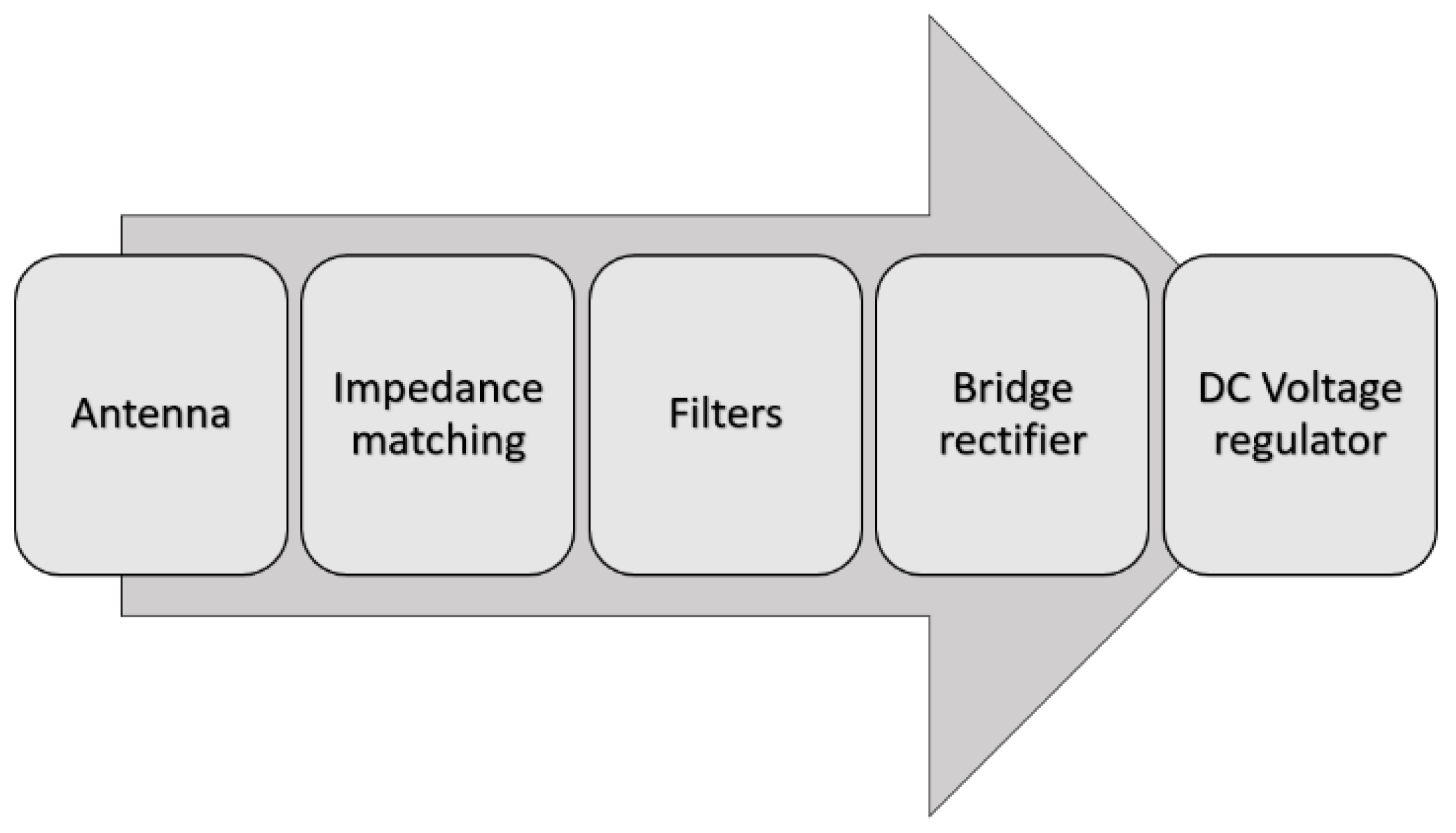
Figure 2.
Bridge rectifier baseline topology.
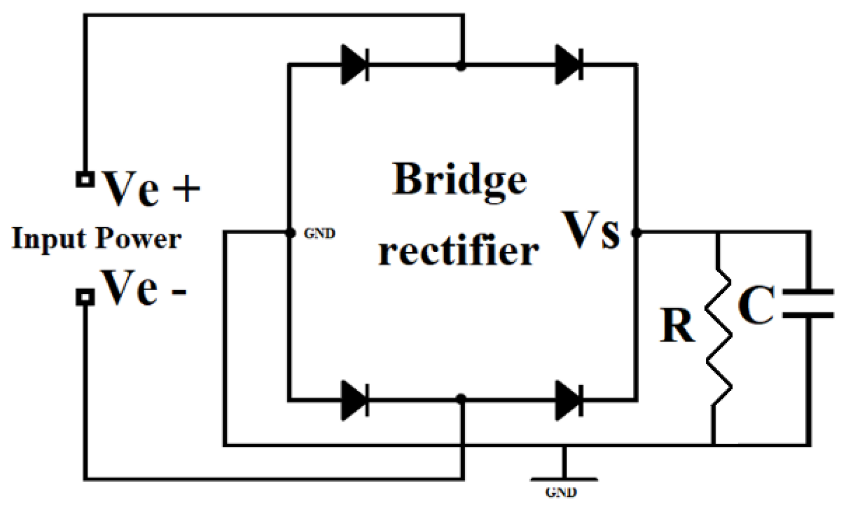
Figure 3.
The PCE as a function of the load resistance (R) using SMS7630.
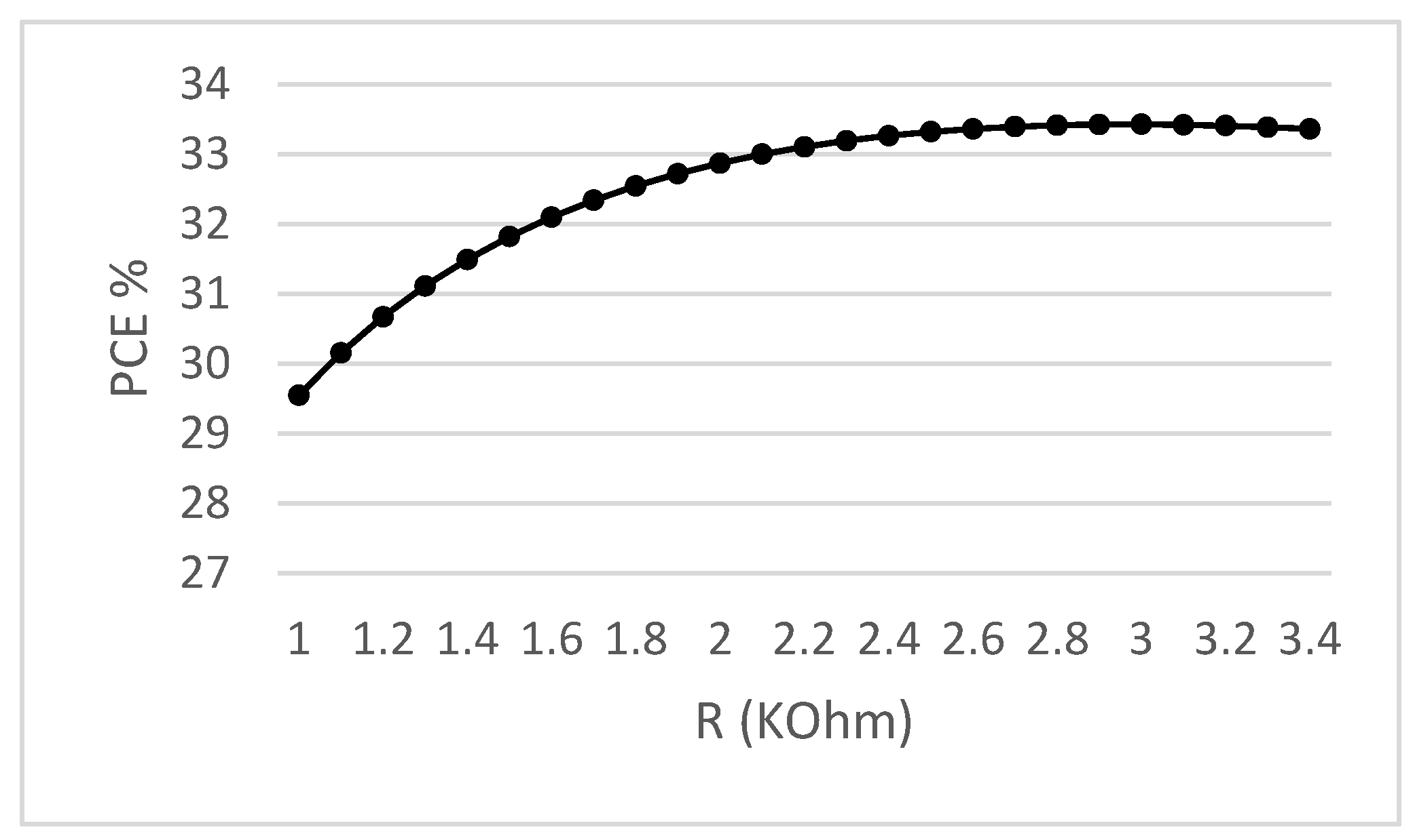
Figure 4.
Rectifier system using LC for impedance matching of SMS7630 bridge diodes.
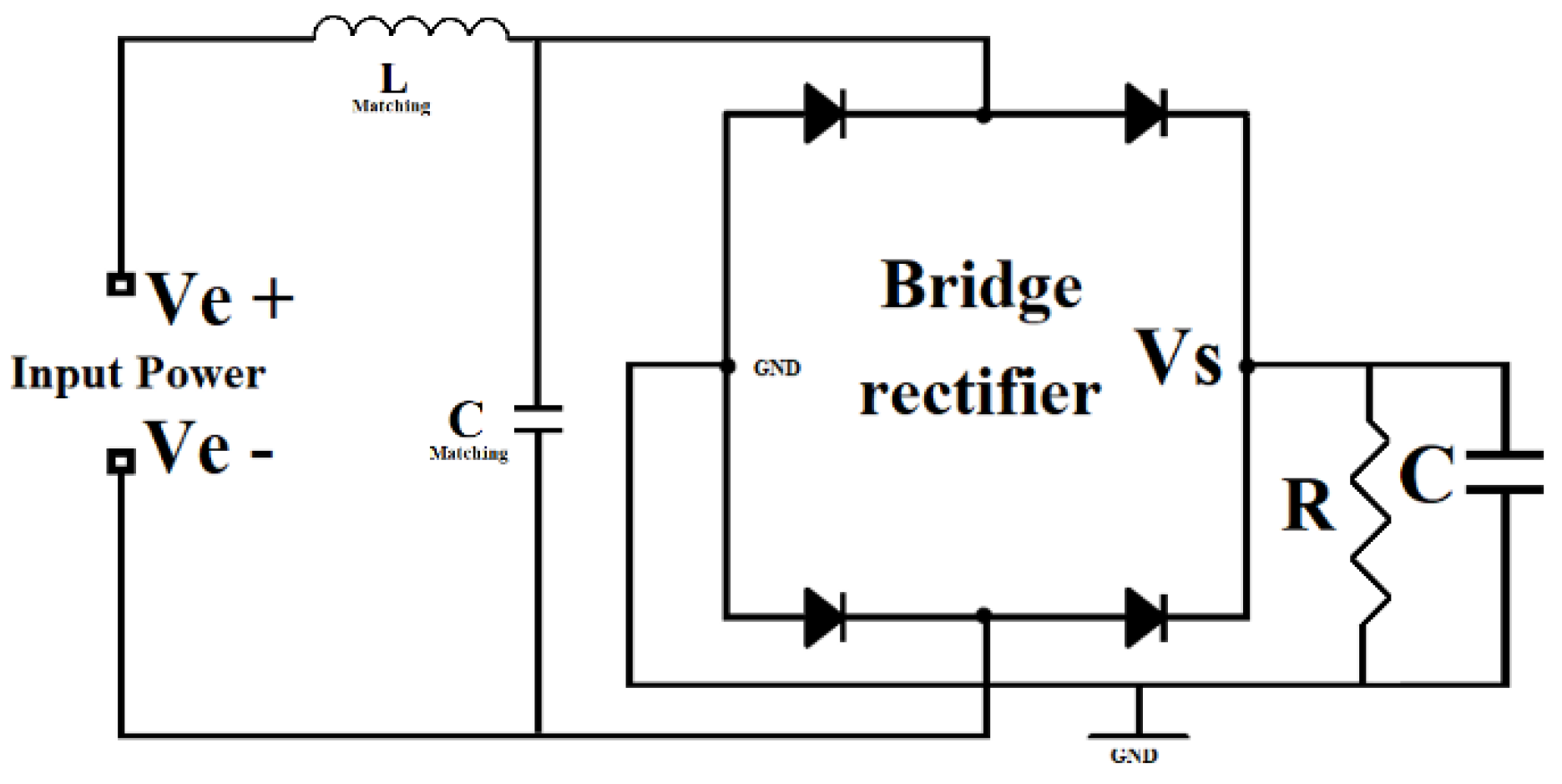
Figure 5.
PCE of both diodes with Pin of -5 dBm and -15 dBm matched with discrete components.
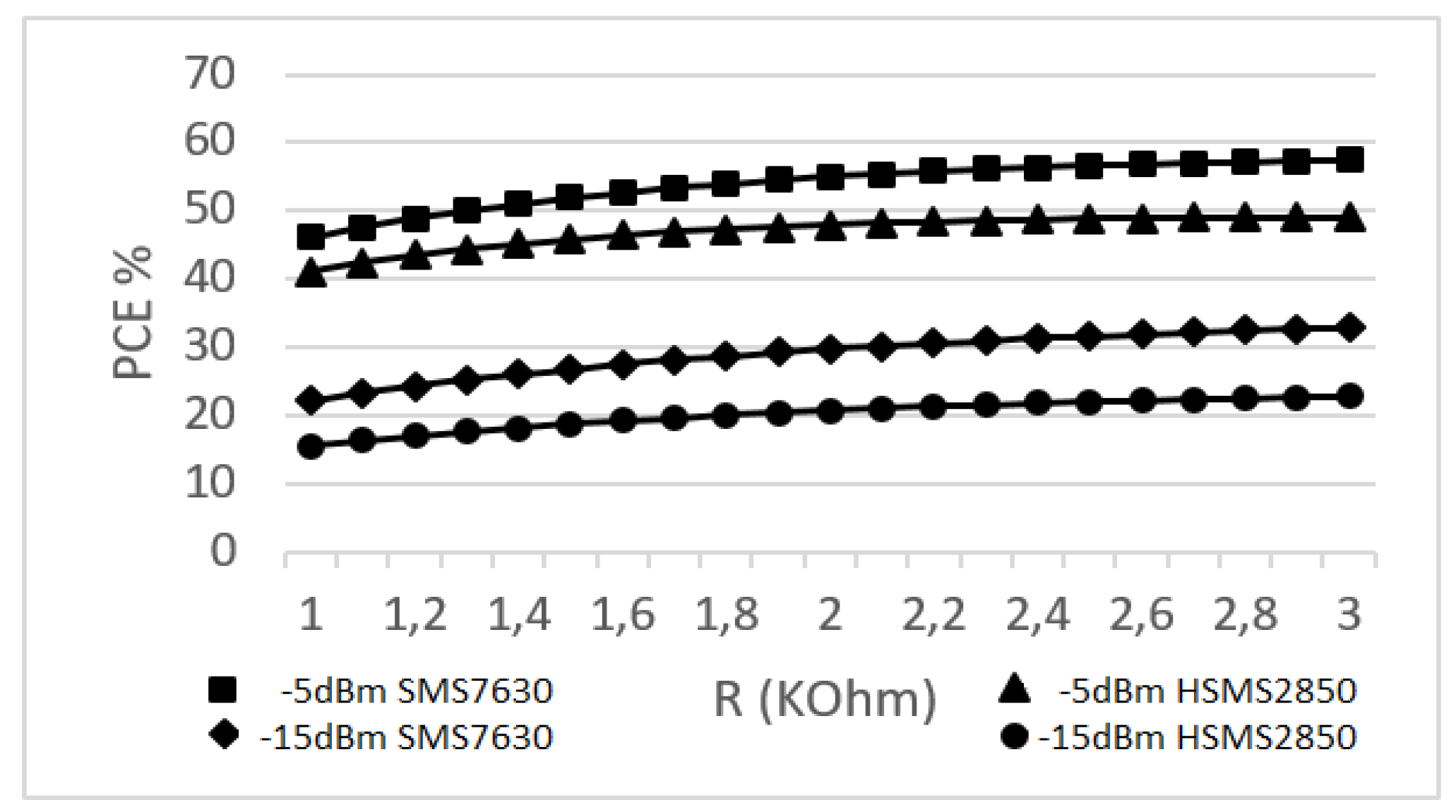
Figure 6.
Bridge rectifier PCB board for laboratory measurement.
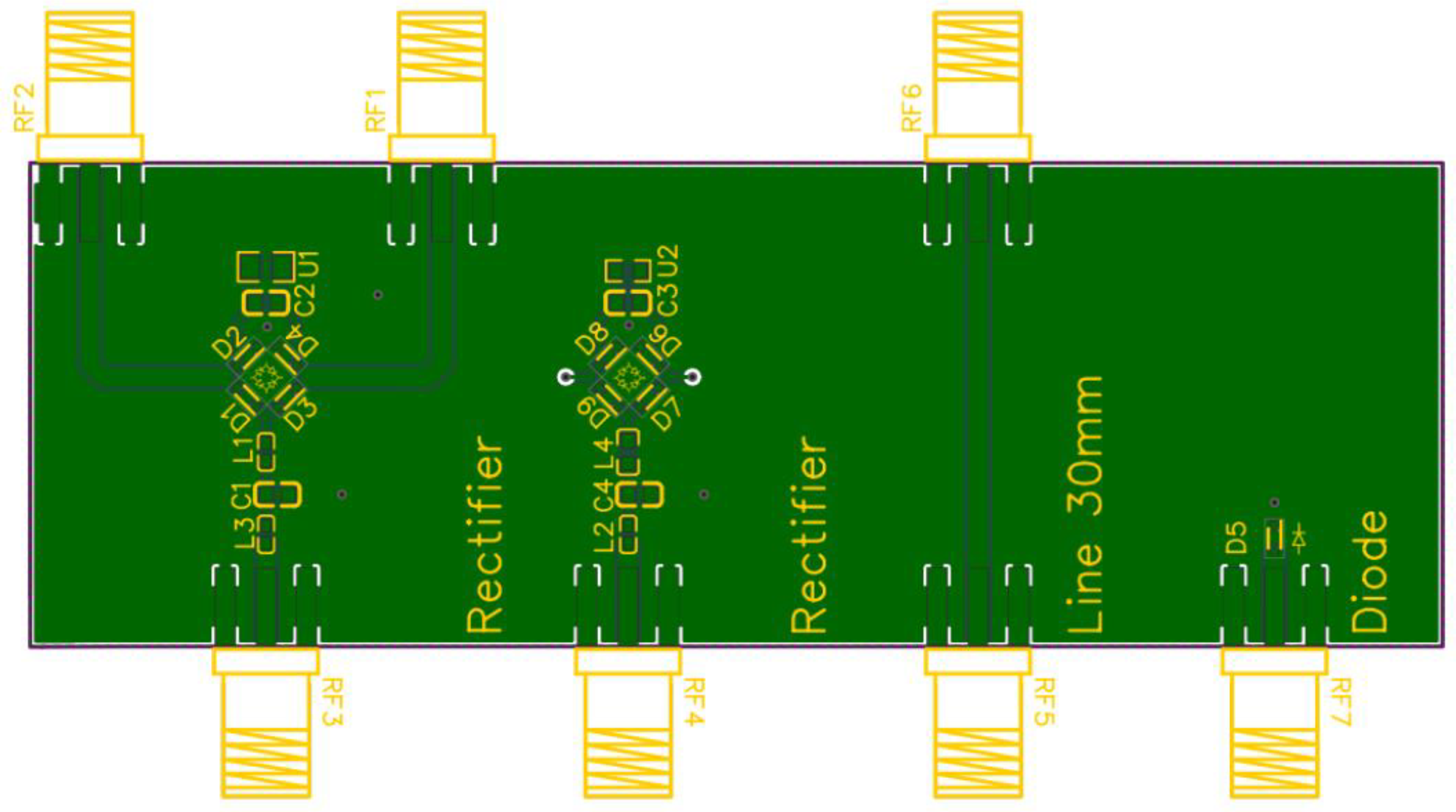
Figure 7.
Full wave Bridge rectifier showing input and output current and voltage.
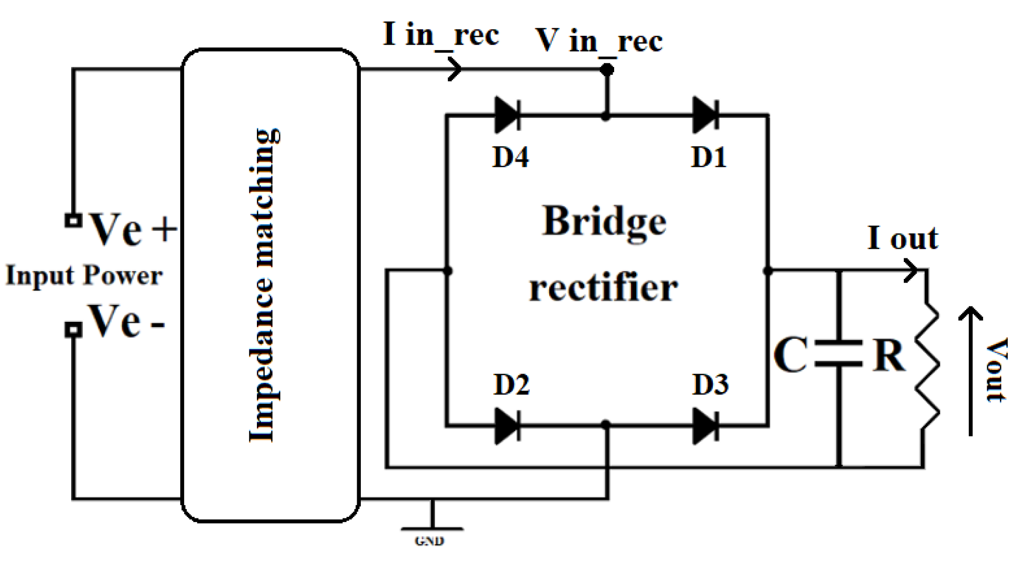
Figure 8.
The equivalent circuit of the bridge rectifier during a rectification cycle.
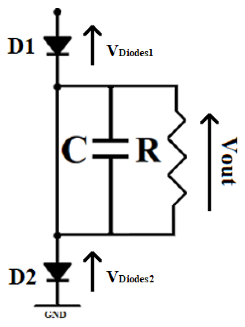
Figure 9.
Full wave Bridge rectifier showing input and output current and voltage with a variation of R load.
Figure 9.
Full wave Bridge rectifier showing input and output current and voltage with a variation of R load.
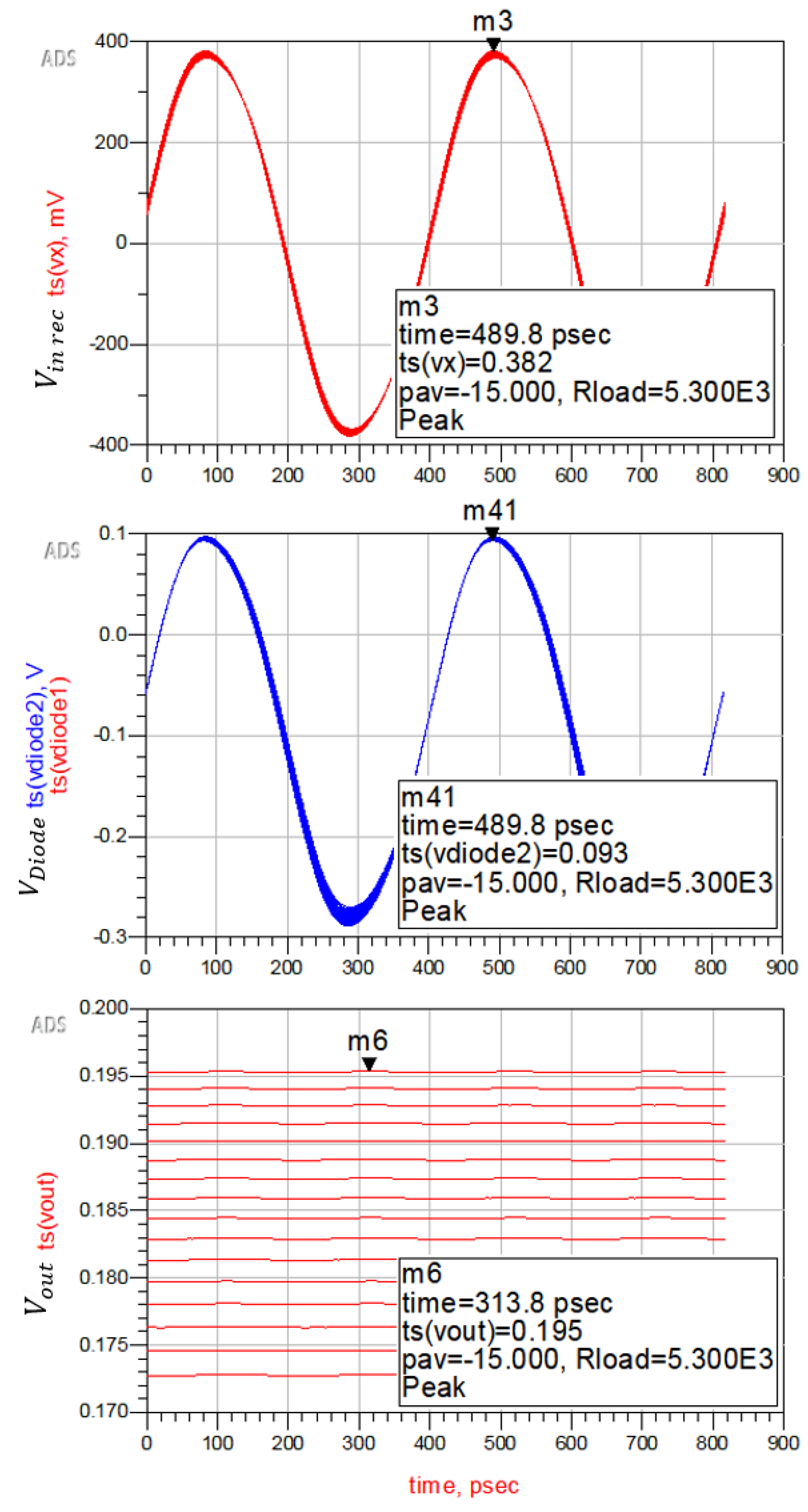
Figure 10.
Current and voltage signal and phase delta at the input of the bridge rectifier.
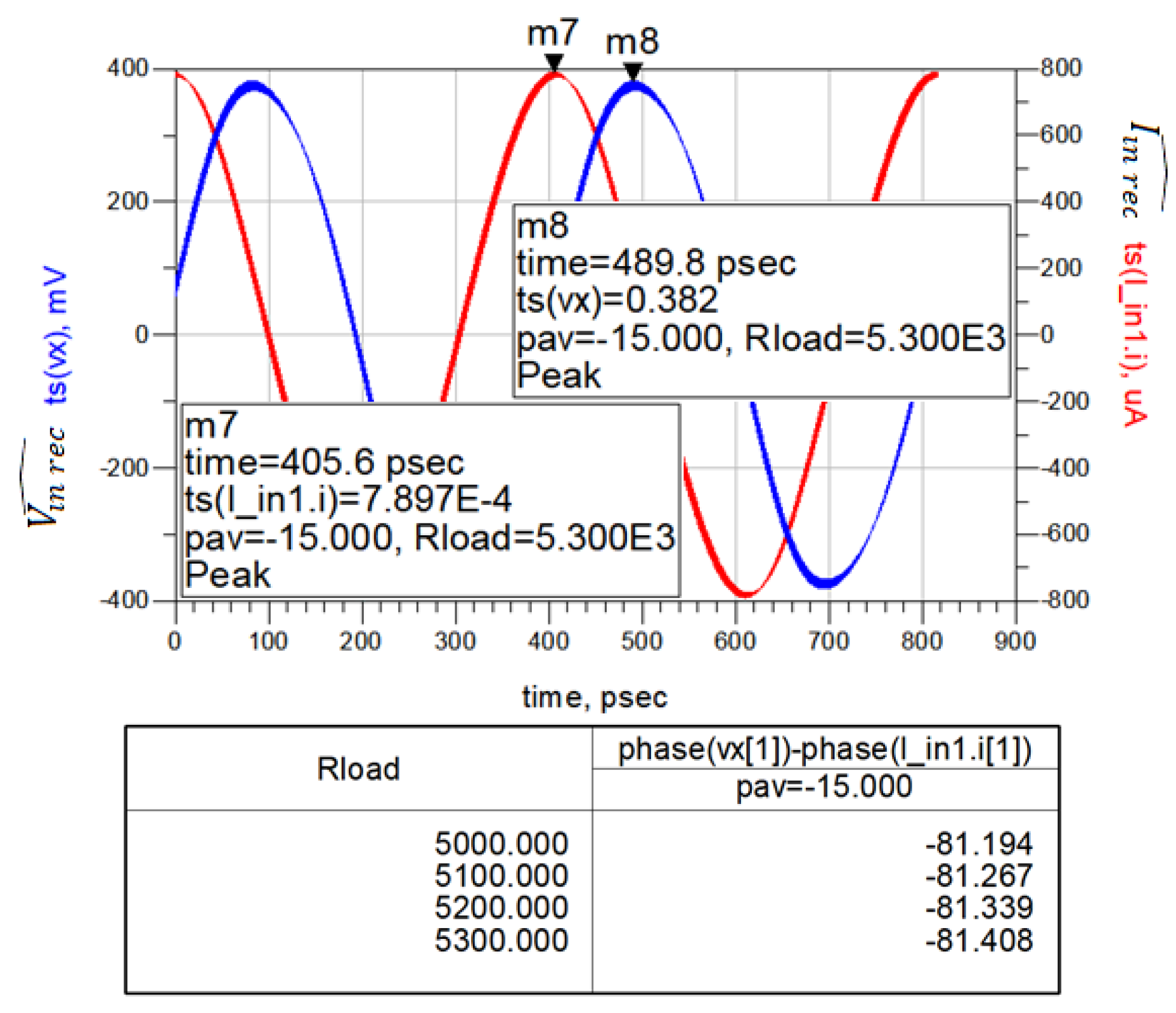
Figure 11.
Current signal at the output of the bridge rectifier.
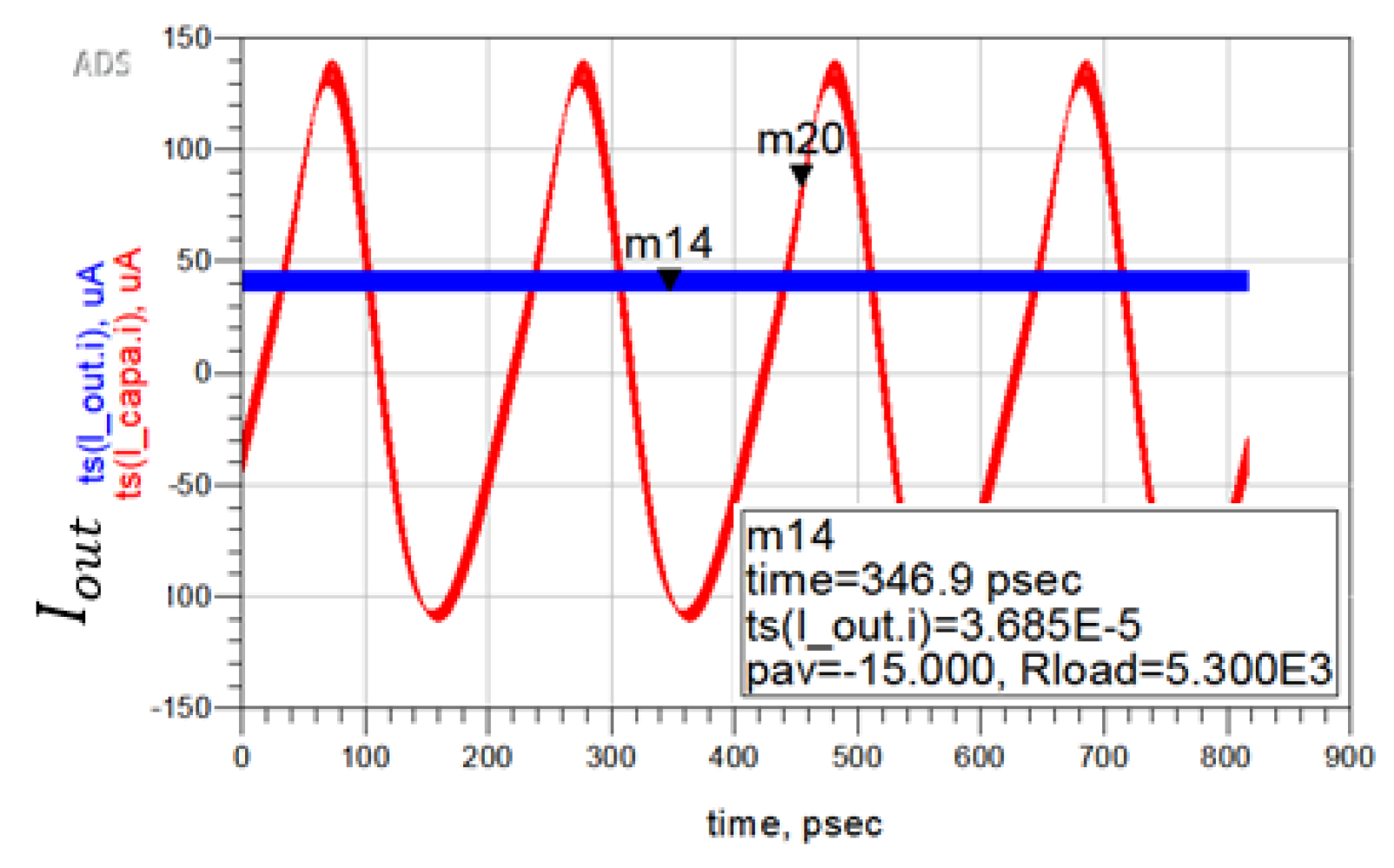
Figure 12.
ADS simulation results of the Bridge rectifier efficiency Pout/Pin.
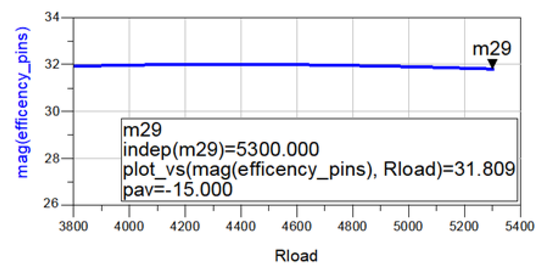
Figure 13.
Schottky diodes voltage double rectifier topology.
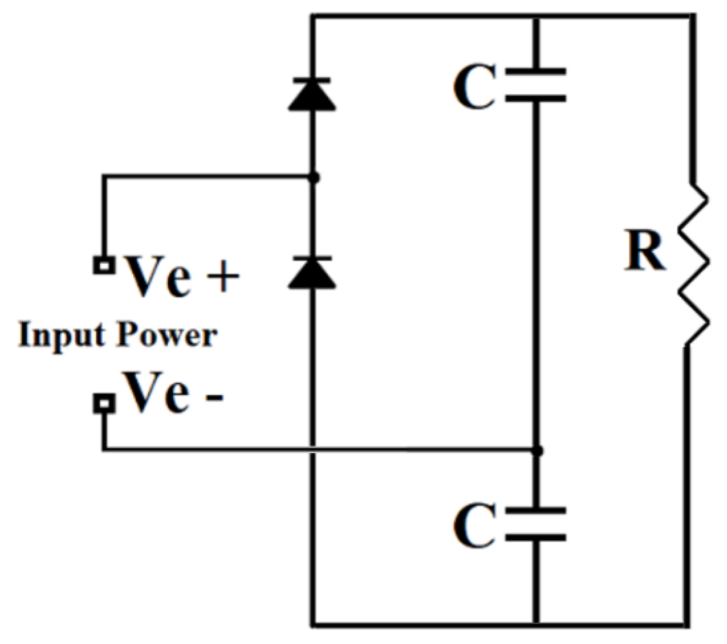
Figure 14.
Variation of Ids with Vds for W = 100 µm and Vgs values ranging from 0.1 V to 0.5 V.
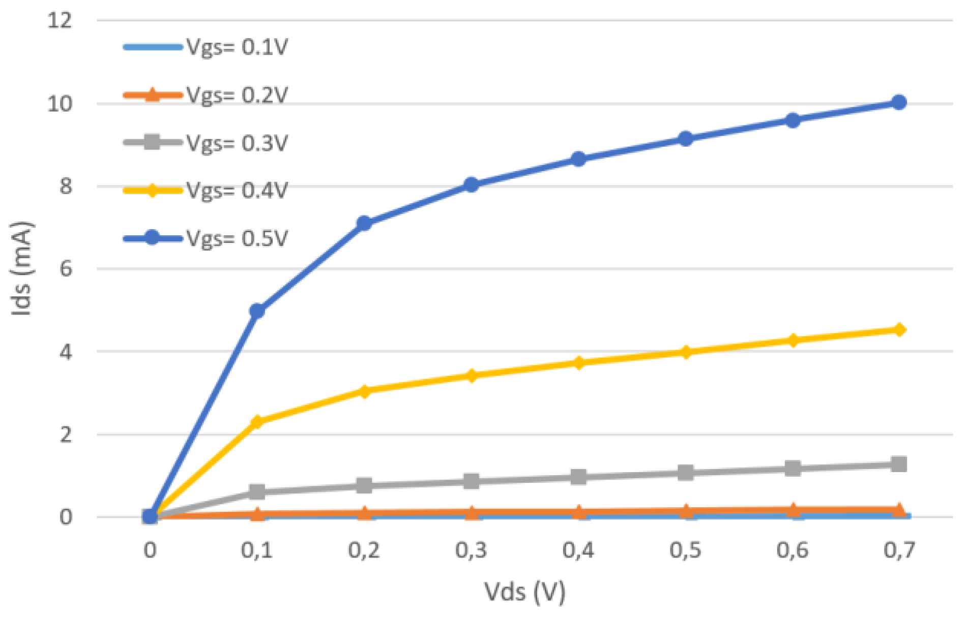
Figure 15.
Ids variation versus Vgs in diode mode for varying W.
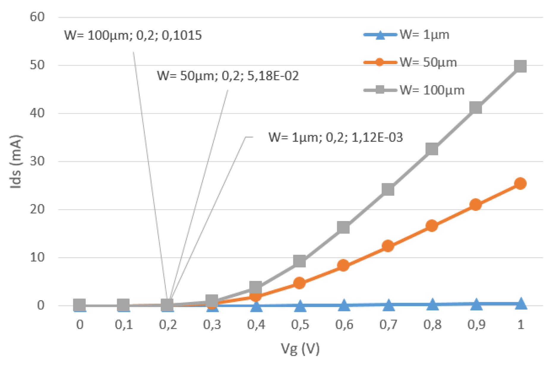
Figure 16.
Half-wave rectifier with NMOS transistor in diode mode (AC signal).
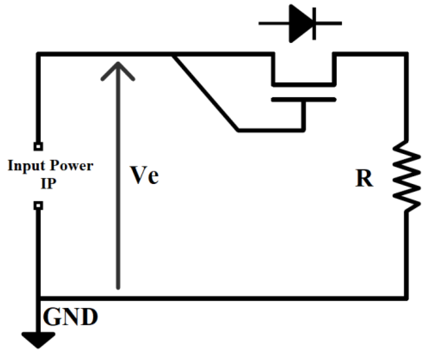
Figure 17.
Half-wave rectifier in diode mode, W = 1 µm, R = 500 Ohms.
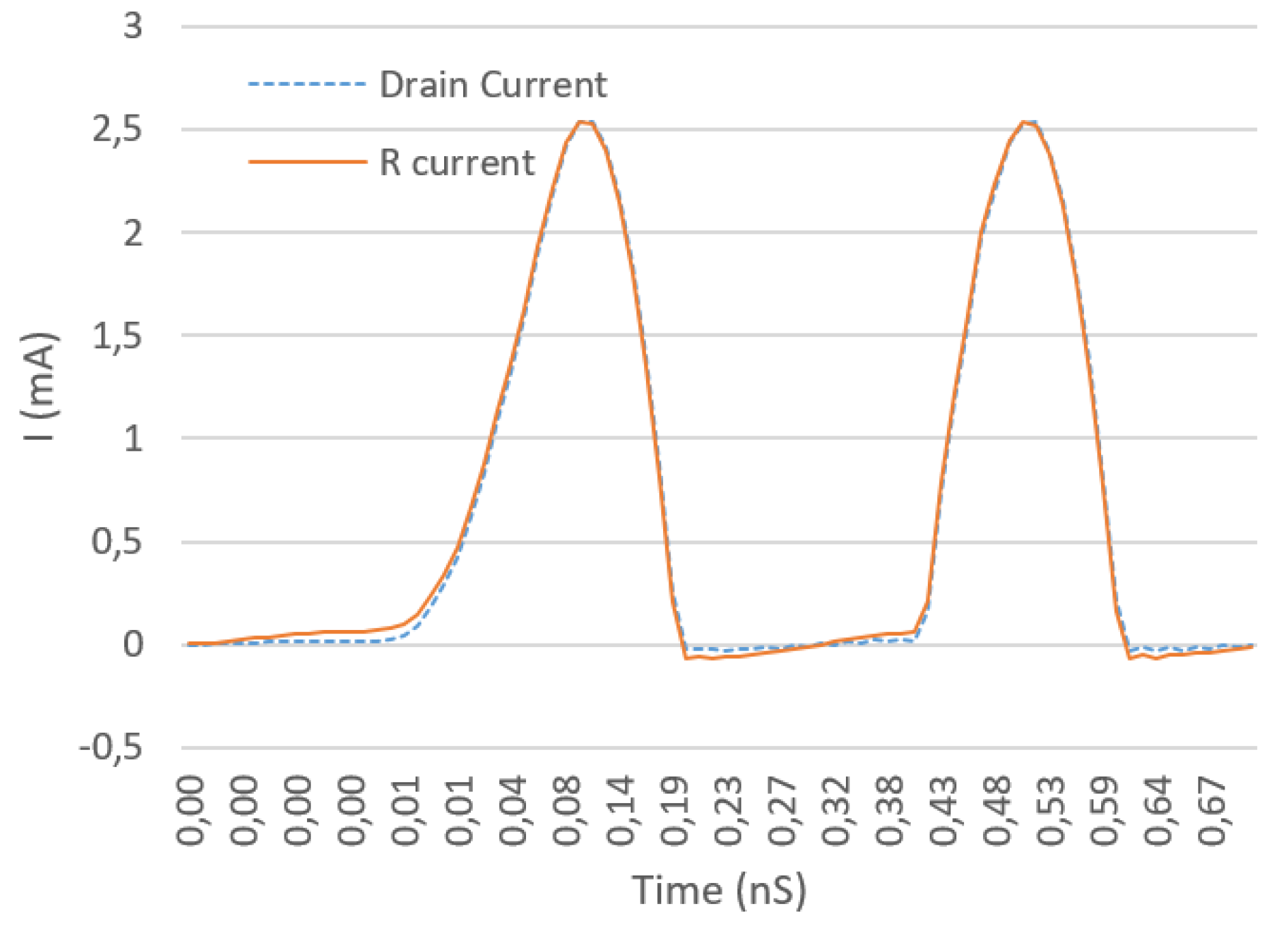
Figure 18.
Half-wave rectifier in diode mode, W = 100 µm, R = 500 Ohms.
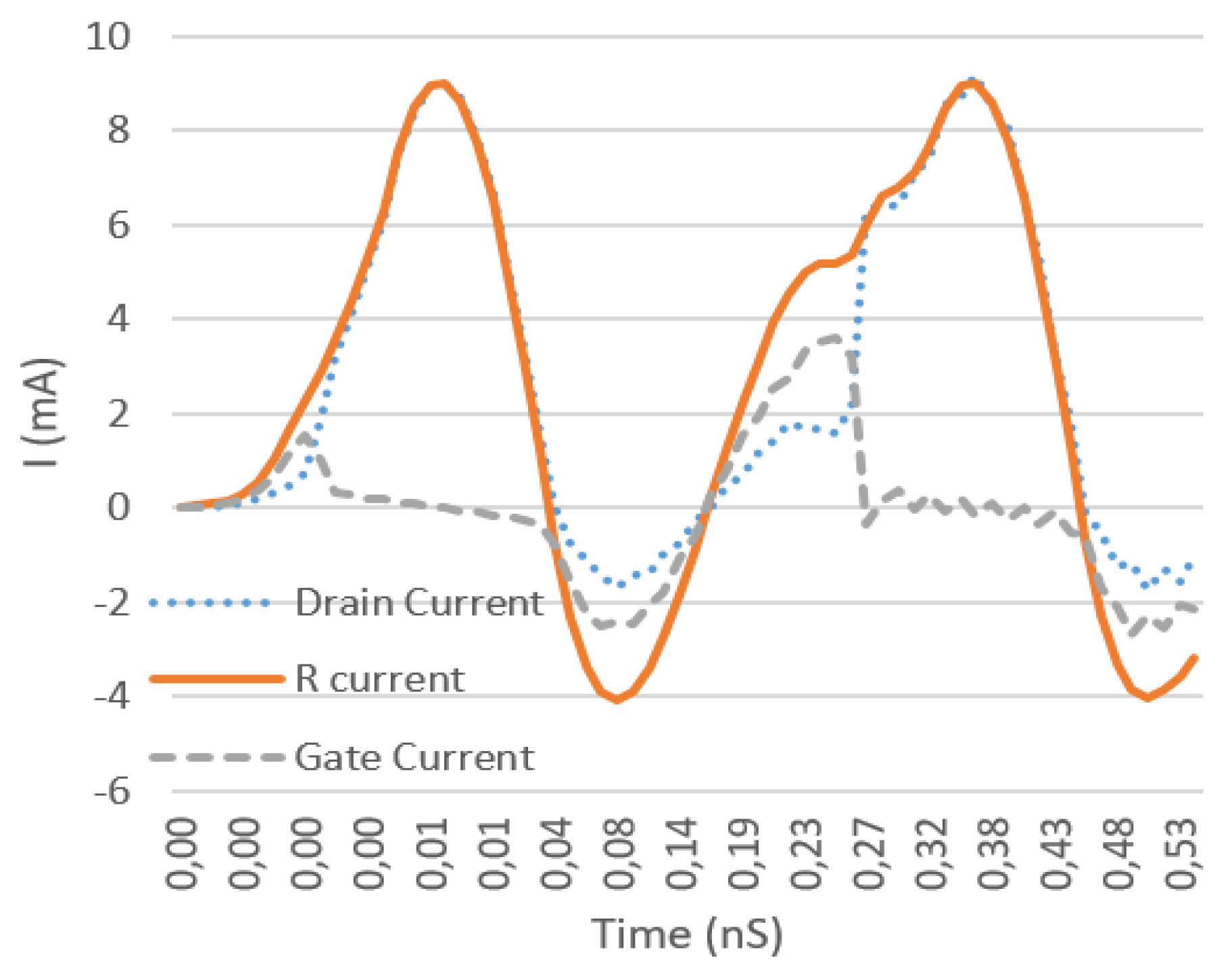
Figure 19.
Half-wave rectifier with NMOS transistor in switch mode (AC signal).
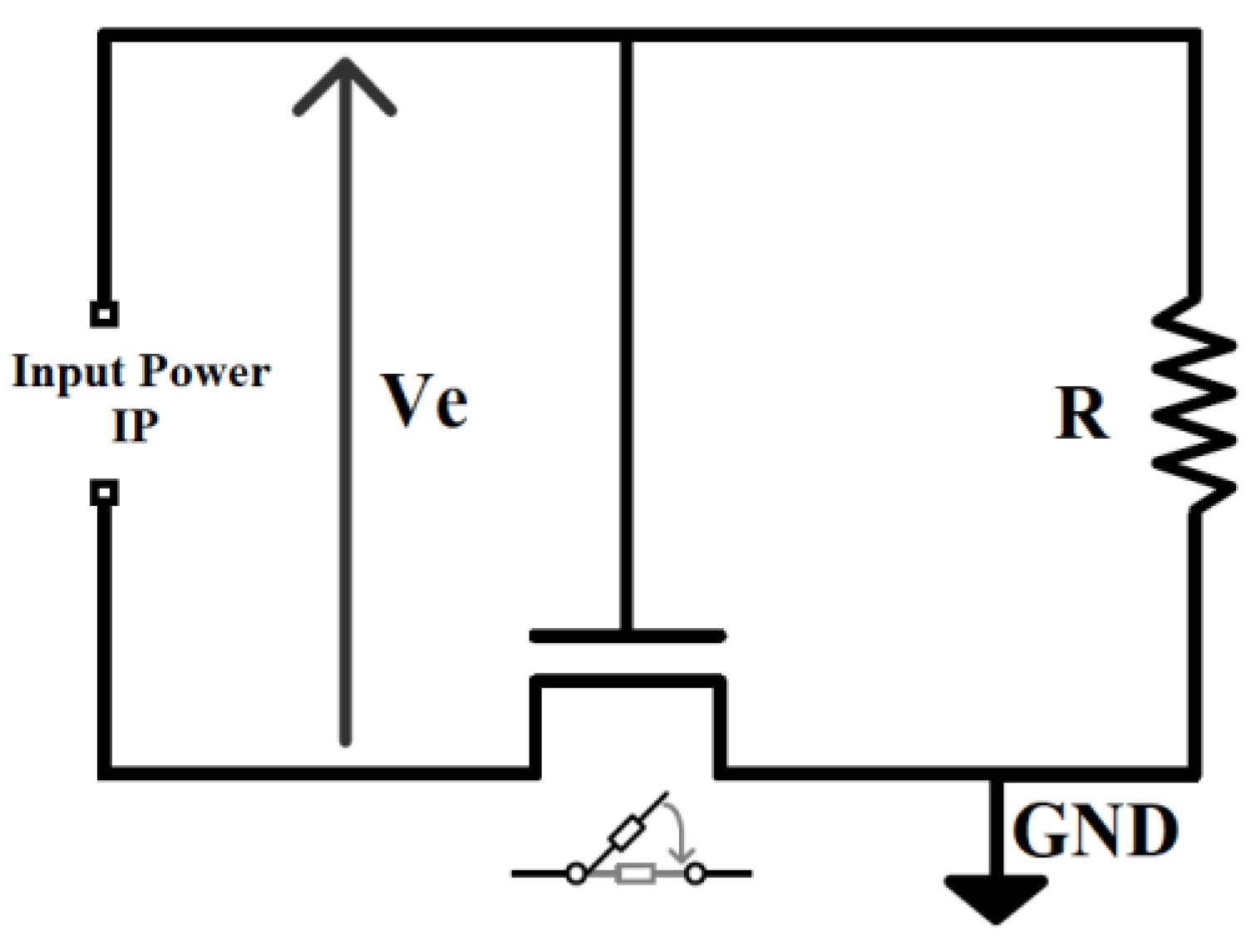
Figure 20.
Half-wave rectifier in switch mode, W = 100 µm, R = 500 Ohms.
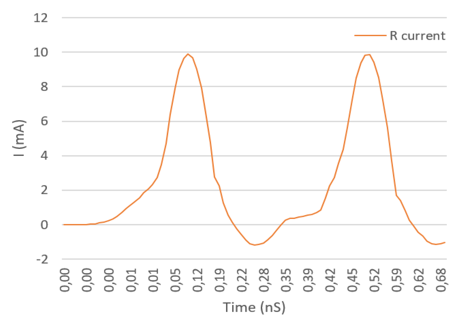
Figure 21.
Equivalent resistance in switch mode for different Vgs values.
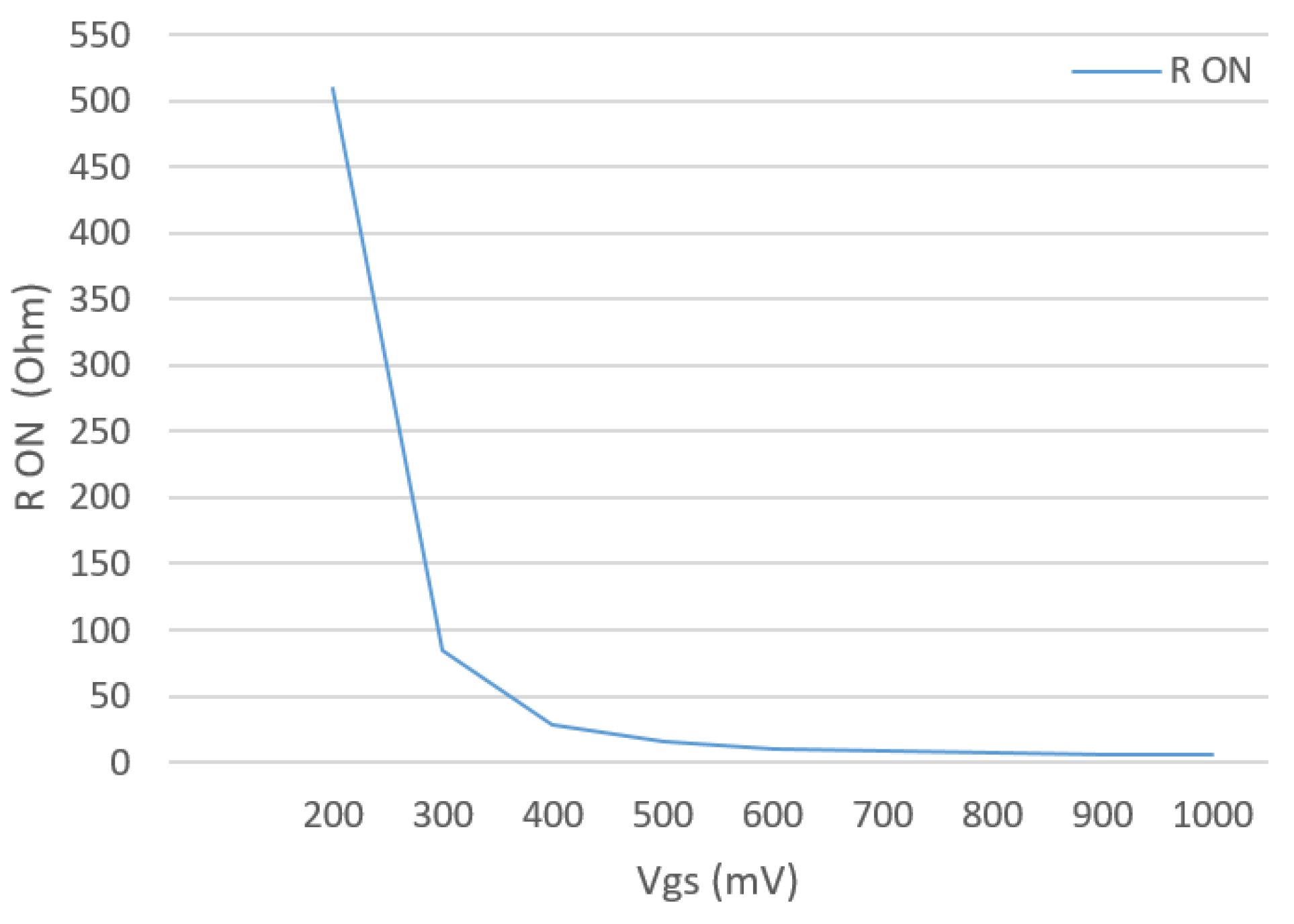
Figure 22.
Equivalent resistance in diode mode for different Vgs values.
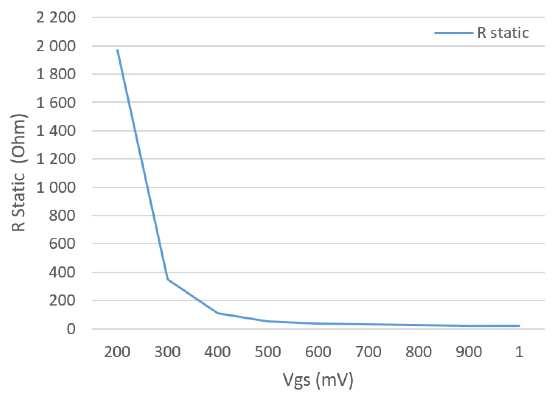
Figure 23.
Full-wave bridge rectifier simulation setup.
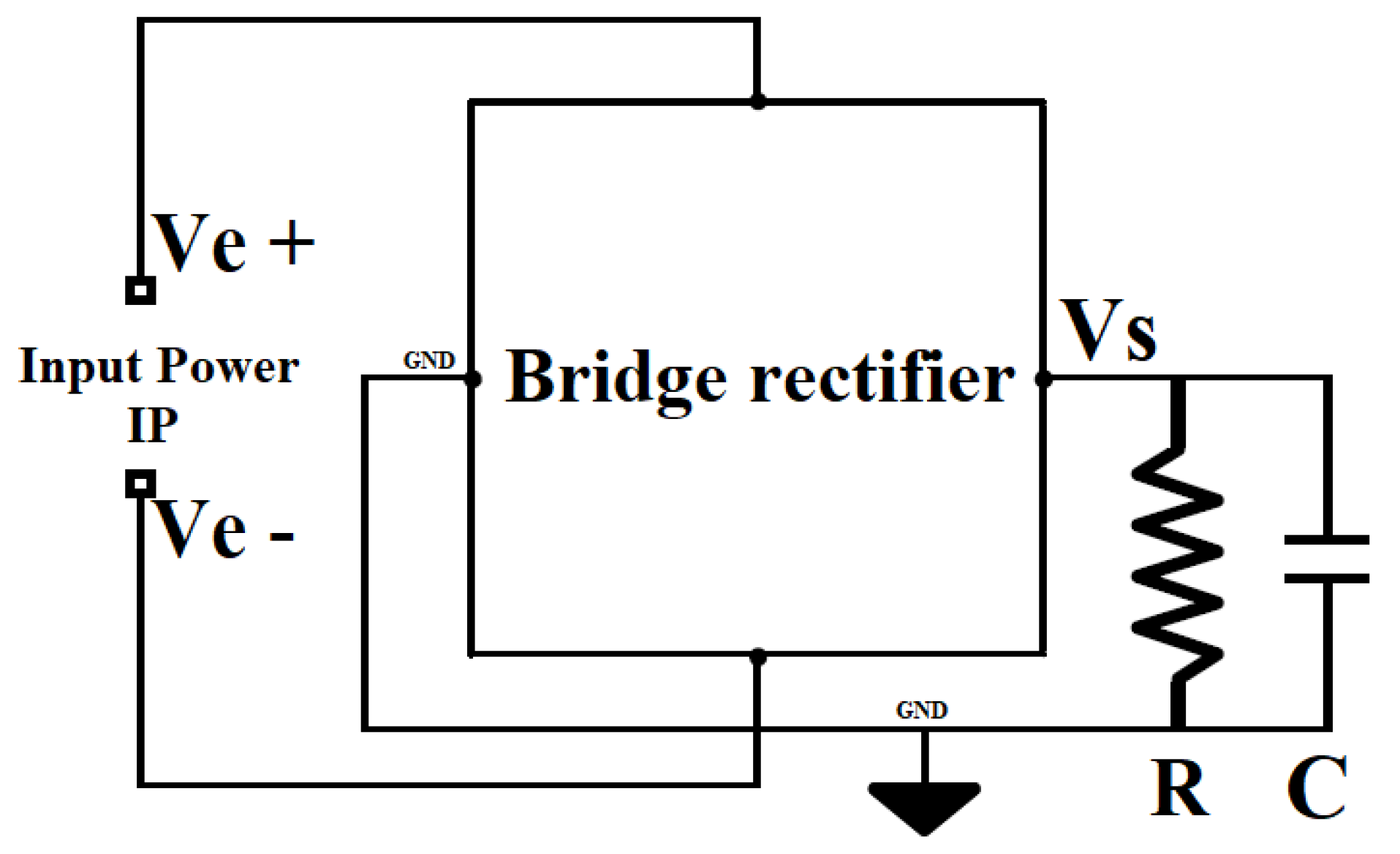
Figure 24.
Configurations of full-wave bridge rectifier topologies: (a) Topology 1, (b) Topology 2, and (c) Topology 3.
Figure 24.
Configurations of full-wave bridge rectifier topologies: (a) Topology 1, (b) Topology 2, and (c) Topology 3.
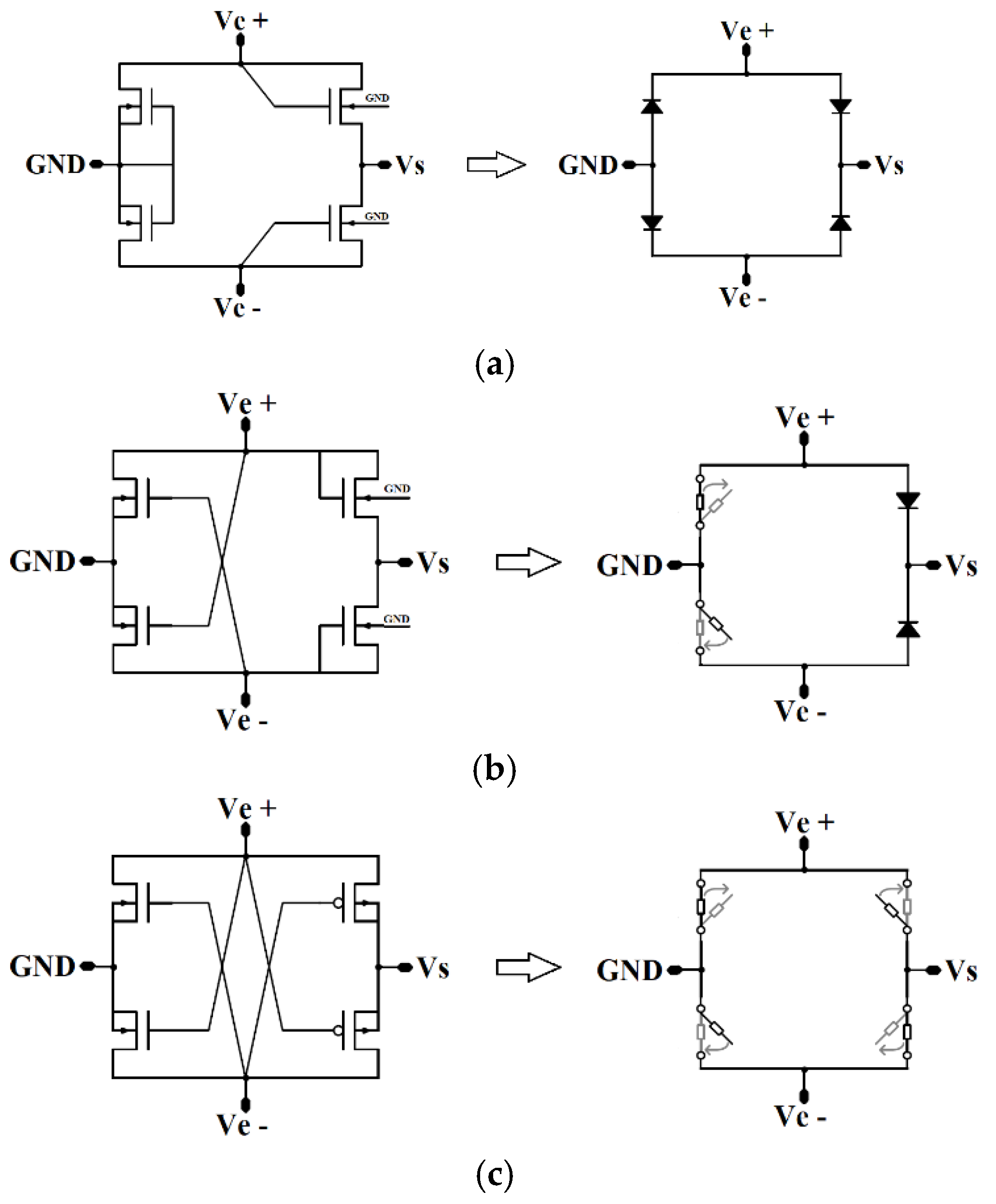
Figure 25.
Eigenvalues of the principal components.

Figure 26.
Eigenvectors decomposition.
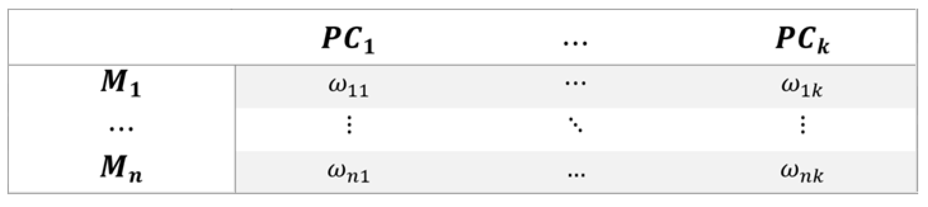
Figure 27.
Synthetic example of the contributions diagram of M1, ... M8 to the PCs.
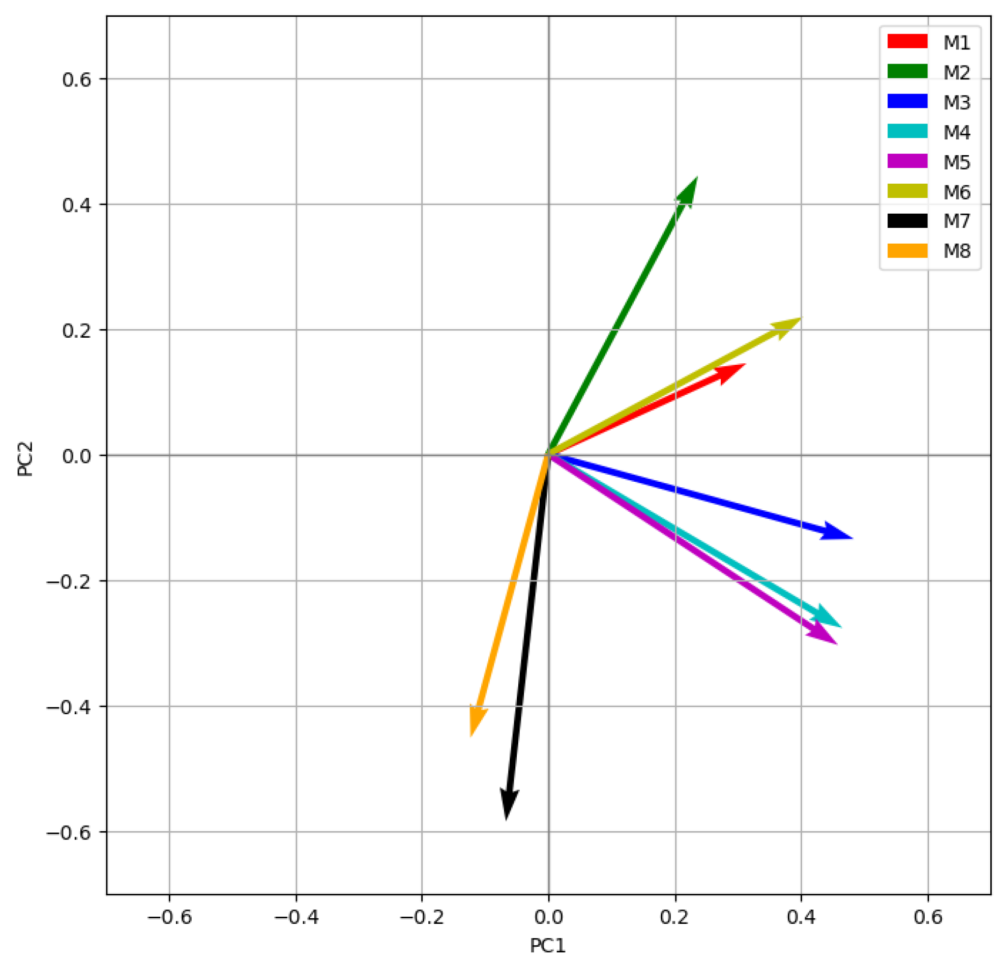
Figure 28.
Synthetic example of PCA biplots a FOM with two principal components.
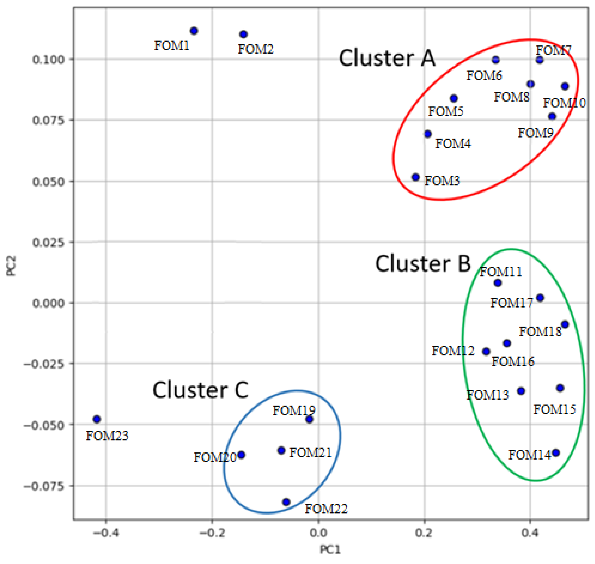

Table 1.
SMS7630 and HSMS2850 spice model parameters.
| SMS7630 | HSMS2850 | |
|---|---|---|
| Rs (ohm) | 20 | 25 |
| Vf (V) | 0.240 | 0.250 |
| Cj0 (pF) | 0.14 | 0.18 |
| Vb (V) | 2 | 3.8 |
Table 2.
The PCE values of the baseline topology.
| HSMS2850 | SMS7630 | |||
|---|---|---|---|---|
| Input Power | -15 dBm | -5 dBm | - 15 dBm | -5 dBm |
| PCE | 24% | 53% | 33% | 60% |
Table 3.
PCE and S11 comparison between the two diodes using discrete components for impedance matching.
Table 3.
PCE and S11 comparison between the two diodes using discrete components for impedance matching.
| HSMS2850 | SMS7630 | |||
|---|---|---|---|---|
| Discrete components | CL | LC | ||
| Input Power (dBm) | -15 | -5 | - 15 | -5 |
| PCE | 23% | 49% | 33% | 57% |
| S11 | < -30 dB | |||
Table 4.
RF POOL RO4350B substrate parameters.
| Substrate | εr | tan δ | Thickness (mm) | Frequency |
|---|---|---|---|---|
| RO4350B | 3.66 | 0.0031 | 1.54 | > 500 MHz |
Table 5.
PCE and S11 comparison between the two diodes using micro strip line for impedance matching.
Table 5.
PCE and S11 comparison between the two diodes using micro strip line for impedance matching.
| HSMS2850 | SMS7630 | |||
|---|---|---|---|---|
| Input Power (dBm) | - 15 | - 5 | -15 | - 5 |
| PCE with Ideal line | 18% | 43% | 33% | 56% |
| PCE with RO4350B line | 16% | 40% | 29% | 52% |
| S11 with RO4350B line | < -40 dB | |||
Table 6.
Overall summary of the different impedance matching options versus the baseline configuration.
Table 6.
Overall summary of the different impedance matching options versus the baseline configuration.
| HSMS2850 | SMS7630 | |||
|---|---|---|---|---|
| Input Power (dBm) | -15 | -5 | - 15 | -5 |
| PCE (Baseline) | 25% | 53% | 33% | 60% |
| PCE (Baseline matched by discrete components) | 23% | 49% | 33% | 57% |
| PCE (Baseline matched by Microstrip lines) | 16% | 40% | 29% | 52% |
Table 7.
Our circuit PCE vs other references.
| Ref | Pin | PCE |
|---|---|---|
| [5] | -5 dBm | 41 % |
| -15 dBm | 27 % | |
| [4] | -6 dBm | 20 % |
| This work | -5 dBm | 57 % |
| -15 dBm | 33 % |
Table 8.
Effect of gate width (W) on Ids with Vds at 0.1 V and 0.5 V for various Vgs in DC polarization
Table 8.
Effect of gate width (W) on Ids with Vds at 0.1 V and 0.5 V for various Vgs in DC polarization
| W(µm) | 1 | 100 | ||||||
| Vds (V) | 0.1 | 0.5 | 0.1 | 0.5 | ||||
| Vgs (V) | 0.4 | 0.5 | 0.4 | 0.5 | 0.4 | 0.5 | 0.4 | 0.5 |
| Ids | 25 µA | 50 µA | 40 µA | 90 µA | 2.5 mA | 5 mA | 4 mA | 9 mA |
Table 9.
DC Power delivered to load R in diode and switch modes.
| DC Power at the load resistance R | ||
| W | Transistor in diode mode | Transistor in switch mode |
| 1 µm | 12.37 µW | 22.64 µW |
| 50 µm | 228.6 µW | 471 µW |
| 100 µm | 365.9 µW | 496 µW |
Table 10.
Output Power and Efficiency Results by Topology.
| Freq = 2.45 GHz | Topology 1 | Topology 2 | Topology 3 |
|---|---|---|---|
| IP = -5 dBm | W = 110 µm, C = 10 pF, R = 650 Ohms | ||
| Output Power | -10.7 dBm | -9.7 dBm | -6.8 dBm |
| Efficiency | 28% | 40% | 69% |
| IP = -26 dBm | W = 110µm, C = 19.95 fF, R = 12.5 KOhms | ||
| Output Power | -35 dBm | -33.8 dBm | -29.8 dBm |
| Efficiency | 13% | 17.8% | 43.6% |
Table 11.
Voltage Efficiency Results by Topology.
| Topology 1 | Topology 2 | Topology 3 | |
|---|---|---|---|
| IP = -5 dBm | |||
| Input Amplitude | 872 mV | 674 mV | 500 mV |
| Output DC | 243 mV | 292 mV | 373 mV |
| Efficiency | 28% | 43% | 75% |
| IP = -26 dBm | |||
| Input Amplitude | 307mV | 220mV | 190mV |
| Output DC | 64mV | 73mV | 113mV |
| Efficiency | 21% | 33% | 59% |
Table 12.
Comparison of PCE of this work with other recent works.
| Ref | Pin | PCE |
|---|---|---|
| [5] | -5 dBm | 41 % |
| This work (diode bridge rectifier) | -5 dBm | 57 % |
| This work (diode voltage doubler) | -5 dBm | 66 % |
| This work (CMOS bridge rectifier) | -5 dBm | 69% |
| [4] | -6 dBm | 20 % |
| [6] | -10 dBm | 35% |
| [5] | -15 dBm | 27 % |
| This work (SMS7630 diode bridge rectifier) | -15 dBm | 33 % |
| This work (diode voltage doubler) | -15 dBm | 41.5 % |
| This work (CMOS bridge rectifier) | -26 dBm | 43% |
Table 13.
List of criteria to be removed with explanation.
| Power storage/retention capability | Redundant with: Isolation between AC Input and DC output Forward vs. reverse current time ratio |
| Impedance matching quality | Redundant with: Matching network efficiency (Pin/Pavailable) |
| Scalability and integration | Out of scope |
| Rectifier sensitivity |
Redundant with: Start-up voltage (Vin) Start-up power (Pin) |
| Component reliability | Out of scope |
|
Cost of technology (MMIC, Discrete components) |
Out of scope |
Table 14.
Final list of criteria.
| Group A: Power conversion efficiency | M1: Antenna gain M2: Matching network efficiency (Pin/Pavailable) M3: Power conversion efficiency (Pout/Pin) M4: Power factor (Pout/Pavailable) M5: Start-up power (Pin) |
| Group B: Voltage performance | M6: Output voltage (Vout) M7: Start-up voltage (Vin) |
| Group C: Current dynamics and energy storage | M8: Forward vs. reverse current time ratio M9: Isolation between AC input and DC output |
| Group D: Signal quality | M10: Harmonic distortion levelsM11: Ripple factor in DC output |
| Group E: Operational stability and reliability | M12: Operating bandwidthM13: Thermal stability |
Table 15.
Data set matrix of circuits and criteria.
| Data set Matrix | M 1 | (…) | M 13 |
| Circuit 1 | (…) | (…) | (…) |
| (…) | (…) | (…) | (…) |
| Circuit N | (…) | (…) | (…) |
Disclaimer/Publisher’s Note: The statements, opinions and data contained in all publications are solely those of the individual author(s) and contributor(s) and not of MDPI and/or the editor(s). MDPI and/or the editor(s) disclaim responsibility for any injury to people or property resulting from any ideas, methods, instructions or products referred to in the content. |
© 2024 by the authors. Licensee MDPI, Basel, Switzerland. This article is an open access article distributed under the terms and conditions of the Creative Commons Attribution (CC BY) license (http://creativecommons.org/licenses/by/4.0/).
Copyright: This open access article is published under a Creative Commons CC BY 4.0 license, which permit the free download, distribution, and reuse, provided that the author and preprint are cited in any reuse.


