Submitted:
17 September 2024
Posted:
18 September 2024
Read the latest preprint version here
Abstract
Semiconductor technology is the backbone of modern innovations, propelling technological advancements in industries such as electronics, renewable energy, telecommunications, and health-related fields. This review expatiates the fundamental properties and working principles of semiconductor materials that determine device performances, while also tracing the historical trajectory of these technologies from the inception of the transistor to pioneering developments, such as tunnel gate transistors and 2D materials like graphene. Specific challenges such as material constraints, manufacturing complexities, and environmental impacts are highlighted. In response to such challenges, measures for the improvement of sustainability, energy saving, and waste minimization in production are discussed. The research also responds to the extended effects of globalization, including the disruptions like COVID-19 pandemic, on supply chain and emphasizes on the importance of developing resilient production frameworks for future growth. Additionally, this work highlights emerging technologies, including quantum computing, artificial intelligence integration, and nanotechnology, which are poised to redefine data processing and storage. The research vindicates the necessity of innovation and sustainability as the key motivators for enhancing the capabilities of semiconductors and global technology.
Keywords:
semiconductor
; microchip
; hardware
; sustainability
; transistors
; manufacturing
1. Introduction
Semiconductors are the essential components of electronics and technology. Since the invention of transistors, these solids have brought revolution in electronics because of their unusual properties [1]. Semiconductors are breakthrough technology with significant potential to drive innovation in modern technology i.e. electronics, renewable energy, and other industries [2]. From early transistors to modern integrated circuits (Figure 1), the Semiconductor industry has transformed global communication and data-processing powers [3]. This industry growth is exponential, with electronic chips being a major constituent in system solutions and serving as drivers for innovation and applications such as GPS positioning or robocab [4].
Diodes and transistors are semiconductor devices that are crucial for contemporary technologies in developing functionalities from smartphones, computers, to medical equipment. Since they are built on semiconductor materials such as silicon, their nature allows for efficient power conversion and signal modulation. The applications of diodes involve rectification; thus, they convert alternating current (AC) to direct current (DC), which is critical for powering an electronic device[5]. They are applied to communication systems, where they help in the modulation of signals for transmission [6]. Transistors basically act as switches and amplifiers and are building blocks of integrated circuits that are applied to most electronic devices[7]. The ability to alter semiconductor properties through doping enhances transistor performance, allowing for the creation of various electronic components [6]. The applications of semiconductors are still growing through developments in artificial intelligence, nanotech, and quantum computing that have spread their use to other fields such as healthcare and energy [1]. The study and development of semiconductors are important as they make up the foundation on which technological enhancements are built in a bid to enhance multiple sectors. It is critical for people inclined to make a difference in contemporary electronics, energy, or communication to have knowledge about semiconductors.
Semiconductor development focuses on long-term sustainability, continuous innovation, and improved functions at lower costs: the industry has evolved from microcomputers to mobile phones; now towards nanoelectronics for even greater functionalities [4]. The industry is however challenged by the recent global chip shortage attributed to the COVID-19 pandemic outbreak [3]. This shortage has highlighted the importance of semiconductor production in global supply chains and the need for resilience in this critical industry. Despite these obstacles, emerging technologies like tunnel gate transistors and graphene promise further innovations in the field.
The geopolitical landscape of semiconductor production has shifted, with Asia, particularly China, becoming a vital center for manufacturing and research [3] due to lower manufacturing costs, supportive policies, and a growing domestic market. However, China’s dependency on U.S. technology for advanced semiconductor designs underscores the global interdependence in this sector [8,9]. China’s growth in semiconductors is driven by strategic policies aimed at reducing foreign dependency, leading to job creation and increased exports [10]. Meanwhile, the U.S.-China technological rivalry intensifies, with the U.S. imposing export restrictions to maintain its dominance [8,11,12]. Despite the shift towards China, the ongoing U.S.-China competition and China’s reliance on American technology highlight the fragility of this global landscape. The future of semiconductor geopolitics will depend on how these nations manage their intertwined interests and dependencies.
This review highlights the generic principles of semiconductors, the revolution and latest advancements in semiconductor technologies, innovative techniques, impending potential development areas that comply with the Sustainable Development Goals (SDGs), and sustainable practices. The goal is to provide a comprehensive guide to semiconductors, prioritizing lesser-known aspects and sustainable practices.
2. Semiconductor Fundamentals
2.1. Semiconductors
Semiconductors are a type of material that possess electrical conductivity between the insulators and conductors used in most electronics [13]. Semiconductors are crystalline solids, which can be characterized by a filled valence band and an empty conduction band with their resistivity alterable [13]. Silicon is the most used semiconductor example because of its properties, which are very suitable for electronic applications. Other examples of semiconductors in use include Germanium (Ge) and Tin Sn as single semiconductors, while Gallium Nitride GaN, Silicon Carbide SiC, and Gallium arsenide GaAs are compound semiconductors. Their ability to conduct electricity can vary significantly based on external conditions such as increased temperature or the presence of specific impurities (dopants) added to it. These external conditions allow them to control electrical current effectively, making them essential in electronic devices like diodes, transistors, and integrated circuits.
The semiconductor conductivity is also strongly influenced by any impurities; interestingly, it has been observed that certain materials exhibit an increase in the level of their conductivity by being less pure [14]. Planar defects in semiconductors, such as stacking faults in Indium Phosphide (InP) can dramatically increase resistivity and depress currents at low voltages [15]. However not all defects affect electrical properties equally; for instance, rotational twin planes in InP have minimal impact [15].
The energy gap between valence and conduction bands also influences conductivity, with larger gaps resulting in lower natural electronic conductivity at ordinary temperatures [14]. Semiconductors are also sensitive to illumination/optical excitation (intensity of infrared, visible light, ultraviolet, or X-rays), magnetic fields, current, or voltage applied to a control electrode, which can affect their conductivity [16,17]. These factors collectively determine the complex behavior of current flow in semiconductors.
2.2. Semiconductor Basics
The major two types of semiconductors are intrinsic and extrinsic semiconductors.
Intrinsic semiconductors consist of only one type of atom, typically silicon (Si) or germanium (Ge) in a crystalline structure (See Figure 2). Conductivity arises solely from thermal generation or recombination of electron-hole pairs [18]. Electrons and holes are present in equal numbers. Conductivity is poor compared to extrinsic semiconductors [18].
Extrinsic semiconductors are derived from intrinsic semiconductors by adding impurities, a process called doping. Doping significantly increases the concentration of charge carriers, greatly improving conductivity [18]. Extrinsic semiconductors are further classified into two; N-type semiconductors and P-type semiconductors (Figure 2). N-type semiconductors are doped with pentavalent impurities like phosphorus or arsenic, resulting in electrons as majority charge carriers. One extra electron from the dopant is freed, becoming a free electron for conduction. P-type semiconductors are doped with trivalent impurities like boron or gallium, resulting in holes (absent electrons) as majority charge carriers. The dopant atom has one less electron, creating an electron-hole that can move through the lattice [18] (Figure 3).
Elemental and Compound Semiconductors are found in Column IV and neighboring columns of the periodic table. The column-IV semiconductors are called elemental semiconductors because they are composed of a single species of atoms. In addition to the elemental materials, compounds of column-III and column-V atoms, as well as certain combinations from columns II and VI, make up the intermetallic or compound semiconductors (See Table 1) [1]. Ternary compounds can also be formed by elements from three different columns – for instance, mercury indium telluride (HgIn2Te4), an II-III-VI compound [19]. They can also be formed by elements from two columns, such as aluminum gallium arsenide (AlxGa1-xAs), which is a ternary III-V compound, where both Al and Ga are from column III and the subscript x is related to the composition of the two elements from 100 percent Al(x=1) to 100 percent Ga (x=0). Pure silicon is the most important material for major semiconductor devices; rectifiers, transistors, and integrated circuit applications, and III-VI binary and ternary compounds are most significant for high-speed integrated circuits (GaAs), light emission and absorption such as LEDs[1,16,19].
2.3. Working Principle of Semiconductors
Energy Band; In semiconductors, electrons are arranged in energy bands. The valence band is filled with electrons tightly bound to their atoms, while the conduction band contains free electrons that can move throughout the material. The energy gap between these two bands is known as the band gap. Semiconductors have a moderate band gap allowing some electrons to jump from the valence band to the conduction band under certain conditions, such as increased temperature or light exposure [20,21] (See Figure 4). Band gap ranges from smaller band gap (Silicon with Eg = 1.1eV) to large band gap (Diamond with Eg = 5.5 eV).
Current Flow Mechanism; In semiconductors, the primary charge carriers are electrons and holes. When an electron gains enough energy (from heat or light), it can move to the conduction band, leaving behind a hole in the valence band. This movement of electrons and holes allows for the conduction of electricity [21,22]. A fundamental component of semiconductor devices is the p-n junction, formed by joining N-type and P-type materials. This junction creates an electric field that allows electrons to flow in one direction while blocking the flow in the opposite direction, functioning as a diode. When a voltage is applied, the depletion zone at the junction can widen or narrow, controlling the flow of current [21,23].
2.4. Historical Development in Semiconductors
Semiconductors are materials that have electrical conductivity properties that fall between those of conductors and insulators [24]. They are the fundamental building blocks of modern electronics and have enabled the development of a wide range of electronic devices from transistors and integrated circuits to solar cells and light-emitting diodes (LEDs).
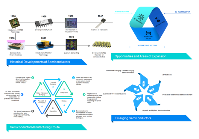
The history of semiconductors traces from the Pre-Transistor Era (See Figure 5). According to G. Busch the term “semiconducting” was used for the first time by Alessandro Volta in 1872 [25,26]. The first documented observation of a semiconductor effect is that of Faraday (1833), who noticed that the resistance of silver sulfide decreased with temperature, which was different from the behavior observed in metals [25]. Johann Hittorf published an extensive quantitative analysis of the temperature dependence of the electrical conductivity of Ag2S and Cu2S in 1851. The history of semiconductors initially focused on two crucial properties; rectification of metal-semiconductor junctions and sensitivity of semiconductors to light [25].
2.4.1. Rectification
Ferdinand Braun invented the solid-state rectifier in 1874, laying the foundation for solid-state electronics [27,28]. He observed the conduction and rectification in metal sulfides probed with a metal point whisker [25]. Although not immediately appreciated, Braun’s discovery later played a significant role in the development of radio and microwave radar systems during World War II [25]. In 1874, Arthur Schuster also observed rectification in a circuit made of copper wires bound by screws. He discovered copper oxide as a new semiconductor when cleaning the ends of the wires removed the rectification effect. In 1929, Walter Schottky experimentally confirmed the presence of a barrier in a metal-semiconductor junction [25].
2.4.2. Photoconductivity and Photovoltaic
The photovoltaic effect at a junction between a semiconductor and an electrolyte was discovered by Alexander Edmund Becquerel (the father of a great scientist Henri Becquerel) [25,29]. Willoughby Smith discovered photoconductivity in solids in 1873 while working on submarine cable testing [25,29]. Adams and Day were the first to discover the photovoltaic effect in a solid material (selenium) in 1876. They noticed that the presence of light could change the direction of the current flowing through the selenium connected to a battery [25]. Charles Fritts constructed the first working solar cell in 1883, consisting of a metal plate and a thin layer of selenium covered with a very thin layer of gold, with an efficiency below 1% [25,29].
2.4.3. Theory of Semiconductor
In 1878, Edwin Herbert Hall discovered that charge carriers in solids are deflected in a magnetic field (Hall effect), which was later used to study semiconductor properties. Several scientists proposed theories of electron-based conduction in metals shortly after the discovery of the electron by J.J. Thomson. Eduard Riecke’s theory (1899) assumed the presence of both negative and positive charge carriers with different concentrations and mobilities [30,31]. Around 1908, Karl Baedeker observed the dependence of the conductivity of copper iodide on stoichiometry (iodine content) and measured the Hall effect in this material, indicating carriers with positive charge. In 1914, Johan Koenigsberger divided solid-state materials into three groups based on their conductivity: metals, insulators, and "variable conductors". Ferdinand Bloch developed the theory of electrons in lattices in 1928 [25,26].
In 1930, Rudolf Peierls presented the concept of forbidden gaps, which was applied to realistic solids by Brillouin the same year. Kronig and Penney developed a simple, analytical model of periodic potential in 1930. Alan Wilson developed the band theory of solids based on the idea of empty and filled energy bands in 1931. He also confirmed that the conductivity of semiconductors was due to impurities. In the same year, Werner Heisenberg developed the concept of holes [25,32]. Walter Schottky and Neville F. Mott independently developed models of the potential barrier and current flow through a metal-semiconductor junction in 1938. Schottky improved his model the following year, including the presence of space charge. Boris Davydov presented a theory of a copper-oxide rectifier in 1938, including the presence of a p-n junction in the oxide, excess carriers, recombination, and the importance of surface states. Hans Bethe developed the theory of thermionic emission in 1942 [25,33,34].
2.4.4. Devices
2.4.4.1. Point-Contact Rectifiers
J.C. Bose obtained a patent for PbS point-contact rectifiers in 1904. G. Pickard was the first to show that silicon point-contact rectifiers were useful in detecting radio waves (patent in 1906). Selenium and copper oxide rectifiers were developed by E. Presser in 1925 and L.O. Grondahl in 1926, respectively. Selenium rectifiers were heavily used in military communications and radar equipment during World War II [25].
2.4.4.2. The P-N Junction
Russel Ohl realized that the problems with the cat’s whisker detectors were caused by the poor quality of the semiconductor material. He melted silicon in quartz tubes and let it cool down, obtaining polycrystalline material with much more uniform electrical properties. This process helped improve the quality and consistency of silicon detectors. Ohl identified the impurities that created the p-n junction he accidentally obtained during his technological experiments and held four patents on silicon detectors and p-n junctions [25,27].
2.4.4.3. Bipolar Transistor
Lilienfeld invented the concept of the field-effect transistor (FET) in 1926 [27,35,36]. Mervin Kelly at Bell Labs initiated a solid-state device group in 1936 foreseeing the limitations of vacuum tubes [27]. Russell Ohl’s work on silicon crystals in the 1940s led to the understanding of n-type and p-type silicon. [27].
The Transistor Invention era occurred in 1947. John Bardeen and Walter Brattain at Bell Laboratories invented the point-contact semiconductor amplifier (transistor action) which exhibited power gain [27,37,38]. They discovered transistor action while investigating surface states in polycrystalline germanium which is also observed in polycrystalline silicon [27,37]. Shortly after, William Shockley developed the theory of bipolar junction transistor in a creative burst, earning him the title of the father of Silicon Valley. However, Bill Shockley was not a co-patent holder on Bardeen and Brattain’s point-contact semiconductor amplifier patent since Julius Lilienfeld had already received a patent in 1930 for what would have been Shockley’s contribution; namely, the field-effect methodology. Shockley received patents for both his minority-carrier injection concept and junction transistor theory, however, and deservedly shared the Nobel prize with Bardeen and Brattain for his seminal contributions to injection, p-n junction theory, and junction transistor theory [37,39].
In February 1948, John Shive demonstrated a correctly operating point-contact transistor with the emitter and collector placed on opposite sides of a very thin slice of germanium, indicating that conduction was taking place in the bulk [25] (See Figure 6). Point-contact transistors were unstable and had hard-to-control electrical characteristics. The first grown junction transistors were manufactured in 1952, although the production process was challenging. In the same year, the alloyed junction transistor was introduced with a simpler production process. In 1954, the first diffused germanium transistor with a characteristic "mesa" shape was reported, featuring a base width of 1 μm and a cut-off frequency of 500 MHz. That same year, Gordon Teal manufactured the first commercially available silicon devices (grown junction), marking a significant breakthrough for electronics. These transistors could amplify and switch electronic signals, paving the way for the development of modern electronic devices [25,39].
2.4.4.4. Metal-Oxide-Semiconductor Field-Effect Transistor (MOSFET)
Julius Lilienfeld obtained patents for devices resembling today’s MESFET (Metal Semiconductor Field-Effect Transistor) and MOSFET (Metal-Oxide-Semiconductor Field-Effect Transistor) in 1930 and 1933, respectively. Oskar Heil applied for a patent for his theoretical work on capacitive control in field-effect transistors in 1934. A group directed by M.M. Atalla worked on the problem of semiconductor surface passivation and found that a layer of silicon dioxide could be the answer. They developed a new concept of a field-effect transistor and manufactured the actual device [25,40,41].
In 1963, Steven Hofstein and Fredric Heiman published a paper on a silicon MOSFET. In the same year, Frank Wanlass proposed the first CMOS circuit. The development of a poly-Si gate led to a self-aligned MOSFET device, where the gate itself constitutes the mask for source and drain diffusion. Reduction of device size led to short-channel effects, which were addressed by reducing the depth of source and drain, using a lightly doped drain, elevated source/drain, or Schottky barrier source/drain [42].
2.4.4.5. The Integrated Circuit
In 1958, two engineers independently developed the integrated circuit (IC), a revolutionary electronic device that combined multiple transistors and other components on a single semiconductor chip. Jack Kilby at Texas Instruments sketched an oscillator circuit that formed in situ in a semiconductor substrate. He fabricated a working model and several logic circuits in the early fall of 1958 and his invention launched the entire field of modern microelectronics [43,44].
Robert Noyce at Fairchild Semiconductor independently showed how to form interconnected transistors, diodes, resistors, capacitors, and other components on a single piece of silicon in 1958-59. Noyce co-invented the integrated circuit, the electronic heart of every modern computer automobile, cellular telephone, advanced weapon, and video games. He co-founded Fairchild Semiconductor and Intel and earned 16 patents in addition to the IC [45,46,47].
The integrated circuit revolutionized electronics, allowing for tremendous advantages in power consumption, speed, reliability, cost, weight, and size compared to circuits made from discrete components [47]. It launched the semiconductor industry, which has grown to over $250 billion in annual sales [48]. The invention of the integrated circuit is considered one of the most important technological breakthroughs of the 20th century.
2.4.4.6. Semiconductor Laser
Semiconductors are crucial for the emission and detection of radiation. The first known phenomenon of light emission in semiconductor material was in 1907 by H. J. Round, with significant contributions from Losev. Semiconductor lasers were, in principle, invented around 1962 by four American research groups. Subsequent research focused on expanding the range of materials and developing new device structures [25].
Herbert Kroemer and Zhores Alferov independently proposed using heterostructures for semiconductor lasers. Alferov, who contributed to the development of the first soviet p-n junction transistor in the same year 1953, understood the possibility of employing double heterostructures in these devices. He developed the first practical heterostructure laser and, along with Kroemer, was awarded the Nobel Prize in Physics in 2000 for advancements in semiconductor heterostructures. The use of quantum wells and new materials, particularly gallium nitride, has significantly advanced semiconductor laser technology [25].
2.4.5. Advanced Devices
2.4.5.1. Tunnel Diode
In 1957 Leo Esaki designed the first germanium tunnel diode, then a silicon tunnel diode in 1958 revealing electron tunneling in heavily doped p-n junctions (Figure 7). Esaki was awarded the Nobel Prize in Physics in 1973 for his work, though Robert Noyce also claimed to have conceived the idea [48,49]. The materials used for this diode are Germanium, Gallium arsenide, and other silicon materials.
Tunneling behavior stems from the tunneling effect which involves the movement of electrons through a thin depletion layer region (Figure 7). In an unbiased tunnel diode, the conduction band of the n-region is coaxial with the valence band of the p-region thereby making it possible for electrons to tunnel in the absence of any voltage and thus making the flow of charge carriers balanced (Figure 7). When a small forward voltage is used, electrons in the n-region move in the p-region resulting in a forward current. As the voltage increases, the overlap between the bands grows, peaking at a certain point (Ip). Beyond this voltage, the current decreases, creating a region of negative resistance (See Figure 7). The tunnel diode, known for its negative resistance due to quantum mechanical tunneling, operates at high speeds and is used in oscillators, amplifiers, and radio frequency (RF) applications [50].
Recent research explores its use in terahertz frequency devices and superconducting spintronic devices, highlighting its versatility and significance in modern electronics [51,52].
2.4.5.2. Silicon-on-Insulator (SOI) MOSFET
Silicon-on-insulator (SOI) MOSFETs offer advantages such as reduced parasitic capacitances, improved device isolation, and reduced short-channel effects due to their structure of a thin silicon layer atop an insulating silicon dioxide (SiO2) layer. Some of the issues that were discovered that limit their use include the deterioration of carrier mobility and the floating body effects. Various extensions and modifications have been proposed to rectify these challenges [53,54,55,56,57].
Quasi-SOI MOSFETs (Figure 8) are a further improvement of SOI MOSFETs which incorporate the features of both SOI and bulk devices. In this structure, the source/drain regions are partially surrounded by an insulator, and the channel is connected to the bulk substrate. This design minimizes the short-channel effects, parasitic capacitances, and self-heating while maintaining effective heat dissipation. Quasi-SOI MOSFETs can be fabricated using epitaxial technology and thermal oxidation, and simulations show they have good scaling capability and can achieve high cut-off frequencies, up to 220 GHz for NMOS and 130 GHz for PMOS (P-type Metal-Oxide Semiconductor) at a 20 nm effective channel length. [53,56].
Localized-SOI MOSFETs (Figure 8) include two variants: quasi-SOI MOSFETs and source-drain-on-nothing (SDON)/source-drain-on-insulator (SDOI) MOSFETs. The quasi-SOI structure is analogous to previously described designs, and the SDON/SDOI devices have recessed source/drain regions on partially buried layers. These structures maintain the advantages of quasi-SOI MOSFETs, such as reduced short-channel effects and parasitic capacitances, and are more compatible with standard CMOS (Complementary Metal-Oxide Semiconductor) fabrication processes, making them suitable for highly scaled devices [56].
DSSB, Dopant-segregated Schottky Barrier SOI MOSFETs (Figure 8) utilize the properties of both SOI and Schottky barrier devices, which include incorporating a thin layer of heavily doped material in the source-to-channel interface. This decreases the Schottky barrier height and increases on-state improvement. DSSB SOI MOSFETs have features like low short-channel effects (SCE), high scalability, and better analog/RF characteristics. However, optimizing the segregation layer density and length is crucial to balance trade-offs between leakage current, drive current, and variability [58,59,60].
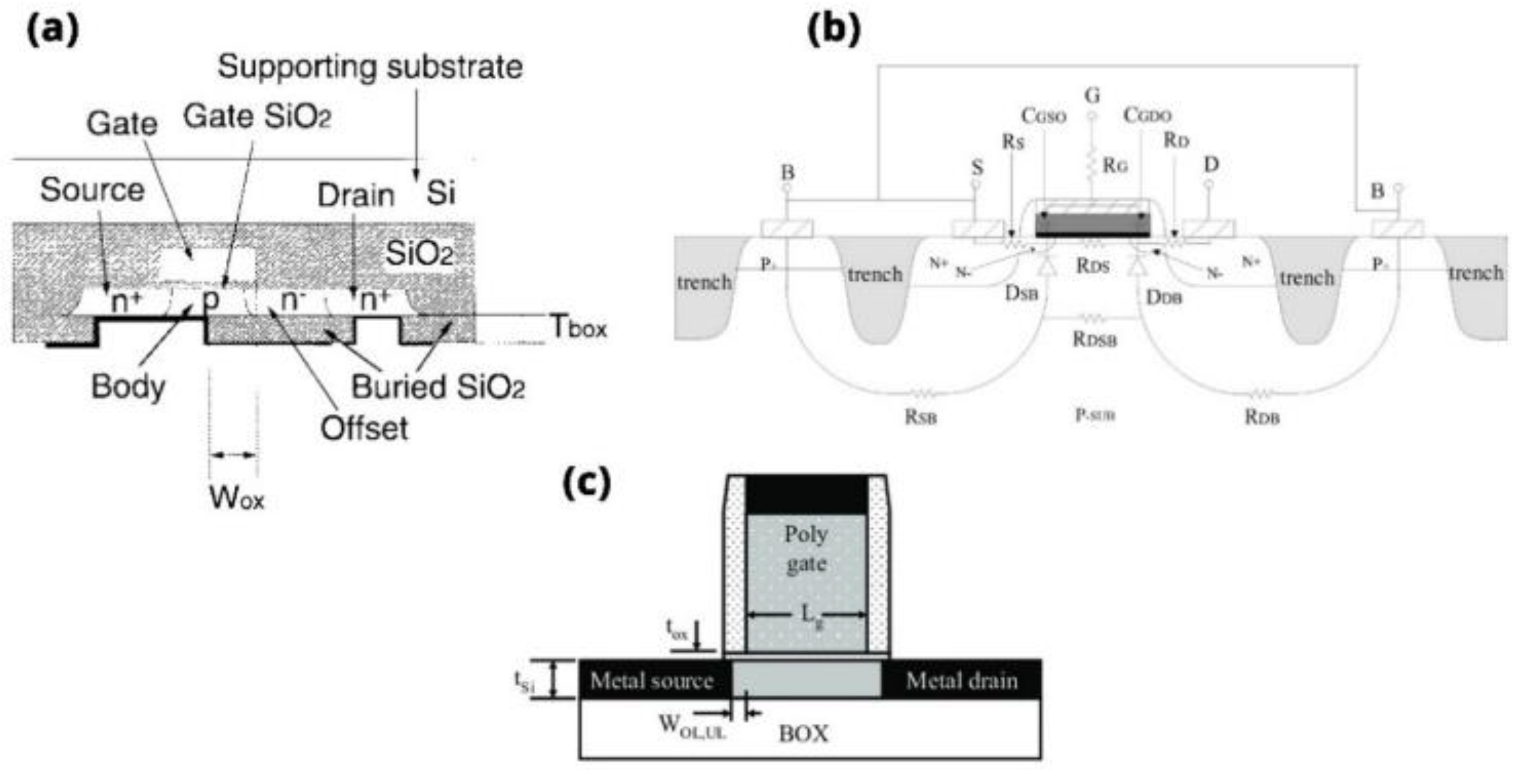
Figure 8.
(a) Quasi-SOI MOSFET cross-sectional diagram [61]. A conventional bulk MOSFET with a lightly doped substrate. The substrate acts as a quasi-insulator, providing some isolation but not as effective as a full SOI structure. (b) Localized-SOI MOSFET cross-sectional diagram [62]. A SOI structure where the silicon layer is partially removed to create a localized island. This improves device performance by reducing parasitic capacitances. (C) Dopant-segregated Schottky barrier SOI MOSFET cross-sectional diagram [63]. A SOI MOSFET with a Schottky barrier at the source and drain junctions. Dopants are segregated to optimize the Schottky barrier height.
2.4.5.2. Multigate Transistors
Advanced structures of transistors, Multigate transistors, which include double gate, FinFET, and surrounding gate structures, significantly improve the electrostatic control and mitigate short-channel effects in metal-oxide-semiconductor field-effect transistors (MOSFETs). These devices, by employing multiple gates, enhance the control of the electric field within the channel, key for scaling down. FinFETs, with their three-dimensional structure and vertically positioned fins, possess better gate control compared to planar devices. Moreover, the double gate transistors lessen the short channel effects like Drain-Induced Barrier Lowering (DIBL), achieve better ON/OFF current ratios, and reduced subthreshold swings which are effective features in low-power devices [64,65,66,67,68,69].
Double Gate Transistors; These are the devices that have two gates (Figure 9) to control the channel so that the channel can be independently biased, hence better electrostatic control. This configuration may improve the overall performance of both analog and digital applications, as confirmed and shown in various simulations [70,71].
Fin Field-Effect Transistor (FinFET); FinFET technology is proven as a promising solution for sub-22 nm technology nodes. The FinFET’s three-dimensional structure (Figure 9) allows for a significant decrease in short-channel effects while achieving high drive currents. Research highlights that FinFETs are capable of providing superior electrical performance, making them ideal for high-frequency applications [66,72].
Gate-All-Around Transistor / Surrounding Gate Structures; These structures, such as Gate-All-Around (GAA) transistors, offer even better control compared to FinFETs by surrounding the channel on all sides (Figure 9). This design minimizes short-channel effects (SCE) and allows for further scaling of device dimensions without significant performance degradation [65,73].
2.5. Other Advanced Devices
Heterostructure Field-Effect Transistors (HFETs) have been acknowledged for their uses at high frequencies and for having superior material characteristics over traditional MOSFETs. The unique combination of materials in HFETs, such as AlGaN/GaN, provides high electron mobility and saturation velocity, which are crucial for high-frequency applications. Available literature shows that these devices are capable of offering very high breakdown voltages coupled with low noise levels, making them suitable for low-power and high-speed electronic applications [74,75,76].
Heterostructure Bipolar Transistors (HBTs) leverage emitter-base heterojunctions to achieve superior performance over conventional BJTs. The use of advanced material in HBTs increases its efficiency and utilization, particularly in high-frequency domains. Research has established that HBTs are capable of astounding electrical characteristics, making them ideal for applications that demand high performance and reliability [74].
Wide Bandgap Semiconductors, like Gallium Nitride and Silicon Carbide, have been accelerating an entirely new frontier of electronics wherein devices can be operated at higher power densities, voltages, and frequencies than conventional silicon-based technologies [77,78]. These materials have larger power density, high efficiency, and thermal stability, with high-voltage operation, making them very suitable for power electronics, renewable energy systems, and electric vehicles [79,80,81]. GaN, owing to superior electron mobility, offers high-frequency performance in RF amplifiers and power converters; on the other hand, SiC excels only in realms of high-power applications adjudged vital by thermal management, like power supplies and industrial motor drives [80]. Wide bandgap semiconductors are finding applications in renewable energy, electric vehicles, and telecommunications, significantly impacting these industries by enabling more efficient, powerful, and compact electronic devices [79,80].
Resistive RAM (RRAM) is an advanced memory technology that employs semiconductor principles, using metal oxides like Titanium Oxide (TiOx) as the switching layer. RRAM operates through resistive switching, where conductive filaments form and rupture within the oxide layer, enabling data storage [82,83]. Key advantages include non-volatility, high speed, low power consumption, and scalability. Recent advancements integrate RRAM with AI to boost performance and unleash forms of computing paradigms, such as neuromorphic computing [84,85]. Not being a conventional semiconductor device itself, RRAM exploits semiconductor materials and principles to achieve better memory performance.
Nanowire transistors are high-performance semiconductor devices that utilize quantum confinement effects to increase carrier mobility and electrostatic control while reducing power consumption and increasing switching speeds. Their vertical surround-gate architecture maximizes gate control while minimizing channel length, essential for maintaining performance as devices shrink. Nanowire transistors can perform multiple functions, such as in neuromorphic computing by controlling charge carriers in different regions. They also address thermal management challenges by optimizing thermal conductivity, crucial for sub-5 nm technology nodes. These innovations make nanowire transistors a significant advancement in semiconductor technology [86,87,88].
Resonant tunneling devices (RTDs) are advanced semiconductor devices that exploit quantum tunneling, allowing charge carriers to pass through potential barriers under specific energy conditions [89,90]. It is this double-barrier quantum well structure that produces resonant peaks in the current-voltage characteristics that allow the RTDs to function at terahertz frequencies, far surpassing traditional transistors. Their operating frequency is way higher than conventional transistors, greatly simplifying circuit designs and hence reducing the number of components required and improving efficiency while diminishing power consumption. RTDs can also be integrated with other semiconductor technologies, such as heterostructure field-effect transistors (HFETs), to create hybrid circuits for ultra-high-speed applications. Their reliance on quantum mechanics marks a significant advancement in semiconductor technology[91,92,93].
2.6. Significance of Semiconductors (Technological, Economic, and Societal Impact)
Semiconductors are one of the core materials and form the backbone of modern electronic devices, which make a wide range of functionalities possible in contemporary technology. Their unique properties and versatility help to a great extent in different applications, ranging from consumer electronics to industrial systems. Key roles of semiconductors in electronics include;
Transistor Functionality; Semiconductors are the primary material used in making transistors, which act as the simplest and building blocks of every electronic circuit. Transistors can function as switches or amplifiers, controlling the flow of electrical current. Such functionality is so very essential to logic operations in a digital circuit and signal processing for microprocessors and memory devices [94].
Integrated Circuits (ICs); Semiconductors have facilitated the miniaturization of electronic components by inventing integrated circuits. ICs integrate thousands to millions of transistors onto a single chip, thus allowing compact and efficient designs that power everything from smartphones to computers. It highly improves performance at reduced size and cost [95,96].
Energy Efficiency; Modern semiconductors, more specifically wide-bandgap materials such as SiC and GaN, have been designed for high efficiency in power electronics. Such materials have superior voltage, frequency, and thermal tolerance compared to conventional silicon, hence having the potential for reduced energy losses and improved thermal management in applications like electric vehicles and renewable energy systems [97,98].
Optoelectronics; Semiconductors have an incredibly large role in optoelectronic devices. They are majorly used for the transformation of electrical signals into optical signals and vice versa. Such devices include light-emitting diodes, laser diodes, and photodetectors. The manipulation of light by semiconductor materials has changed display technology, telecommunications, and lighting solutions completely [99,100,101].
Flexible and Organic Electronics; Advancements in organic semiconductors have led to the development of flexible electronic devices, such as organic light-emitting diodes (OLEDs) and organic photovoltaics. These materials allow for lightweight, bendable, and even wearable electronics, expanding the possibilities for consumer products and applications in health monitoring [102,103].
Sensors and IoT Devices; Semiconductors drive the development of sensors that detect physical phenomena, such as temperature, light, and motion. These inherently form a part of the Internet of Things, which enables smart devices to capture data and send them to improve areas like automation and connectivity in healthcare, agriculture, or smart cities [99,104,105].
High-Speed Communication; Semiconductors have found use in different kinds of communication devices, including fiber optics and wireless networks, which have facilitated data transfer at higher speeds. Semiconductor lasers and photonic devices aid high-speed information transfer; this forms part of the internet structure and mobile communication [99,106,107].
The semiconductor industry is vital to the global economy, driving economic growth, job creation, and technological advancement [10]. It supports various sectors, such as IT, telecommunications, and automotive, and has shown resilience during challenges like the COVID-19 pandemic [106,108,109]. Its role in international trade, particularly between major economies like the US and China, underscores its significance [110]. The industry’s innovation and adaptability are crucial for sustaining economic growth.
2.7. Focus on Semiconductor Sustainability
Many more sustainable materials are being considered for production within the semiconductor industry to decrease environmental impact and dependence on toxic compounds. Major examples of such attempts are the development of Kankyo-Semiconductors based on abundant and less toxic elements, such as silicon, iron, aluminum, calcium, and magnesium, in lieu of the traditional materials in optoelectronics. [111]. Additionally, there is a high demand for environmentally friendly solvents and components free from lead during the process of fabrication of perovskite solar cells to achieve devices with better performance while having a minimum detrimental impact on the environment [112].
Alternative substrate materials for printed circuit boards (PCB), such as polyimide and paper-based substrates, along with lower-temperature solders, are also being explored to reduce the environmental impact of electronic products [113]. Niobium-based semiconductor materials are being researched for their potential in the utilization of photocatalytic applications, such as solar fuel production, which can contribute to renewable energies and decrease dependency on fossil fuel sources [114].
3.0. Emerging Semiconductors3.1. Wide-Bandgap Semiconductors
Wide-bandgap (WBG) semiconductors, especially silicon carbide (SiC) and gallium nitride (GaN), are emerging as third-generation semiconductor materials; they possess superior properties compared to conventional semiconductors like silicon [115]. These materials have high saturated drift velocity and a high critical breakdown field (See Figure 10). These materials are also appropriate for high-power, high-temperature, and high-frequency applications (see Figure 11) [115,116]. Recent research has also focused on ultrawide bandgap (UWBG) semiconductors, which have bandgaps wider than 3.4eV of GaN, including high Al-content AlGaN, diamond, and Ga2O3 [117]. These UWBG materials show promise in high-power and RF electronics, deep-UV optoelectronics, quantum information, and extreme-environment applications [117]. Ongoing research aims to address challenges and advance the state-of-the-art in WBG and UWBG semiconductor technologies.
3.2. Quantum Dot Semiconductors
Quantum dot semiconductors are nanomaterials that have special electronic and optical properties attributed to their size-dependent quantum effects. These semiconductor nanostructures confine excitons in three spatial dimensions, exhibiting discrete energy levels akin to atoms [124]. Quantum dots have been endeavored in a wide range of applications, like photoelectrochemistry sensors, with simple, fast, and miniaturized solutions for analyte detection [125]. One of the factors that makes this class so attractive for organic photoredox transformations is the tunability of its redox properties [126].
Initially cadmium-based, quantum dots have evolved to include alternative materials with reduced toxicity such as germanium, silicon, and carbon, while retaining unique photonic properties in drug development and delivery [127]. A small change in one of the parameters, like size or shape, will alter the electronic and optical properties of quantum dots, therefore making them tuneable for desired applications that range from optoelectronics to biomedical diagnostics.
3.3. 2D Materials
Two-dimensional (2D) materials, such as Transition Metal Dichalcogenides (TMDCs), graphene, and black phosphorus, have emerged as promising semiconductors for electronic and optoelectronic applications due to their unique properties like atomic thickness, excellent electronic structure, and high mobility [128,129,130,131,132,133]. These materials adhere to other substances through van der Waals interactions, enabling compatibility with different material platforms for on-chip light sources and photodetectors, potentially offering a universal on-chip light source scheme for Photonic Integrated Circuits (PICs) [130].
2D semiconductors have several advantages in ultra-thin devices with atomic scale thicknesses and allow the creation of nanoribbons and heterostructures [134]. These materials have a highly tunable bandgap, which may be engineered with controlling layer numbers, strain engineering, chemical doping, and external electric fields, thus offering an alternative for applications that lie within various spectral regions from terahertz to ultraviolet [135]. Engineering atomic-scale defects in TMDCs can enhance carrier transport and improve future electronic technologies, pointing out the need for understanding electron-defect interactions of these materials [136].
Even though the performance is high and energy-efficient, several challenges remain to be overcome in terms of stability, material quality, dielectric integration, contact formation, and preparation methods before 2D semiconductor materials find large-scale production and application [129]. Ongoing research focuses on improving growth techniques, understanding charge carrier scattering mechanisms, and addressing short-channel effects to realize the full potential of 2D semiconductors in future electronic devices [133,134]. With such challenges being surmounted, prospects presented by 2D materials in revolutionizing semiconductor technology are very high, and their potential to foster advancements in the development of high-performance and energy-efficient electronic and optoelectronic devices is at its inception stage.
3.4. Organic Semiconductors
Organic semiconductors, primarily composed of carbon-hydrogen bonds, exhibit semiconductor behavior and can be doped to create N- and P-type materials, enabling the construction of devices like organic light-emitting diodes (OLEDs), organic field-effect transistors (OFETs), and organic solar cells [137]. These materials are made up of π-bonded molecules or polymers, often including heteroatoms like nitrogen, sulfur, and oxygen, and can exist as molecular crystals or amorphous thin films (Figure 12). They typically behave as insulators but become semiconducting upon charge injection, doping, or photoexcitation. They hold a large bandgap and a low dielectric constant [138].
The carrier mobility of organic semiconductors is influenced by factors such as energy, morphology, and solvent choice, impacting crystallinity and molecular ordering. Techniques like cyclic voltammetry and ultraviolet electron spectroscopy are essential for understanding charge transport mechanisms [139]. Single-crystal organic semiconductors are recognized as central to high-performance devices attributed to unique optoelectronic properties because of weak van der Waals interactions [140]. Hyperbranched polymers (HBPs) are also notable for regulating charge transport and film morphology [141].
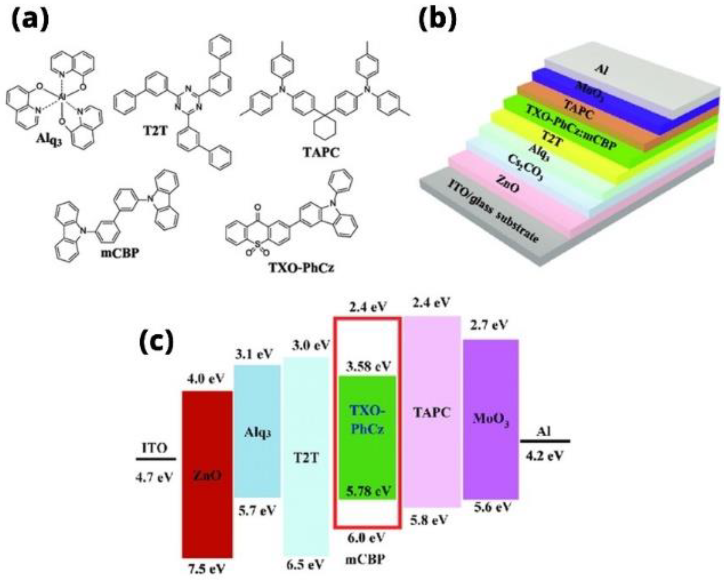
Figure 12.
Organic Semiconductors; (a) Molecular structures of the organic semiconductors for the inverted OLEDs; (b) scheme of the inverted OLEDs; and (c) the energy levels of the materials involved in the inverted OLEDs [142].
Figure 12.
Organic Semiconductors; (a) Molecular structures of the organic semiconductors for the inverted OLEDs; (b) scheme of the inverted OLEDs; and (c) the energy levels of the materials involved in the inverted OLEDs [142].
Techniques to fabricate organic semiconductors include vacuum deposition, solution processing, and self-assembly, with methods such as spin-coating and inkjet printing enabling the realization of flexible/wearable electronics [143]. Applications include OLEDs, organic photovoltaic cells, OFETs, and biosensing devices. Organic semiconductors have some very attractive features associated with them, relating to mechanical flexibility, low cost, and ease of fabrication that make them very attractive in a wide range of electronic and optoelectronic applications [138].
3.5. Perovskite Semiconductors
Perovskite semiconductors, with their remarkable optoelectronic properties and versatile applications, have emerged as a promising class of materials, particularly in photovoltaics and other optoelectronic devices [144]. Characterized by a general formula of ABX3, with A and B as cations and X as an anion, usually a halide or oxygen, these materials have high optical absorption, high carrier mobility, long diffusion lengths, and unique ambipolar charge transport properties [145,146].
Perovskite solar cells have seen rapid advancements, achieving power conversion efficiencies exceeding 25% in just over a decade [147]. Their excellent photophysical properties and solution-processability have also led to applications in light-emitting diodes, photodetectors, lasers, and X-ray scintillators [147]. The ability to tailor perovskite properties by manipulating their crystal structure, size, and composition has further enhanced their functionalities, making them valuable in applications like photocatalysis and radiation detection [148]. In the domain of radiation detectors, lead halide perovskites like CsPbBr3 demonstrated high efficiency in X-ray and gamma-ray detection and thus can be an important material for imaging applications [149].
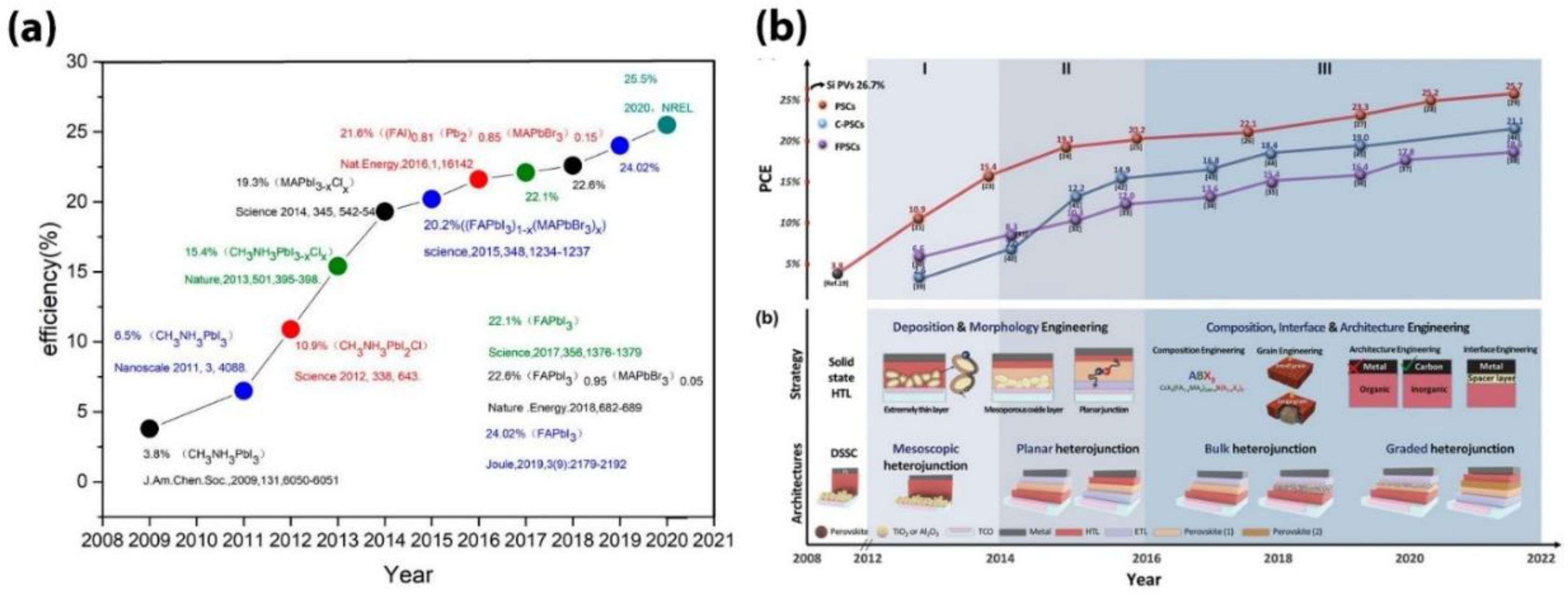
Figure 13.
Perovskite Semiconductors; (a) The evolution of the efficiency of perovskite solar cells (PSCs) from 2008 to 2020 [150]. (b) Chronological evolution of the PCE of perovskite solar cells (PSCs), C-PSCs, and FPSCs and a brief history of schematics for fabrication strategies and device architectures in PSCs (HTL: hole-transport layer, ETL: electron-transport layer, TCO: transparent conductive oxides, PV: photovoltaic) [151].
Despite their rapid progress, perovskites face challenges in stability, reproducibility, and toxicity. Issues such as ionic transport can introduce defects and degrade performance, necessitating strategies to mitigate these challenges [152]. Understanding the fundamental chemistry and physics of perovskites is essential for addressing these issues and guiding future developments [144].
Environmental concerns have heightened interest in finding alternatives to lead-based perovskites. Research is still focused on developing the stability, efficiency, and scalability of perovskite-based technologies. The incorporation of PbS quantum dots into perovskite matrices, for instance, enables sub-bandgap photocurrent generation; this could fundamentally open up prospects for overcoming traditional efficiency limits in solar cells [153]. As the field progresses, the development of stable, high-performance perovskite devices holds great promise for revolutionizing optoelectronics and renewable energy technologies.
3.6. Hybrid Semiconductors
In particular, hybrid semiconductor materials that have gained much attention today are porous metal halide semiconductors and organic-inorganic hybrid semiconductors, owing to their great properties and potential applications. PMHS spanned by the Spanopoulos group [154] reveal excellent water stability and broadband light emission, which makes them very promising for solid-state batteries and photonic crystals. On the other hand, organic-inorganic hybrid semiconductors, such as the ones explored by Yawen Li et al. [155] in their paper, exhibit specific optoelectronic properties and thermodynamic stability that enable next-generation optoelectronic applications. Such hybrid materials take advantage of the assets of both organic and inorganic components in terms of tailored properties and functionalities, making them very promising for several technological innovations related to, among others, electronics, photonics, and energy storage technologies [156,157,158].
3.7. Porous Semiconductors
Porous semiconductors have garnered significant research attention attributed to their unique properties due to their porous structure (Figure 14) and potential applications. Some key properties include increased surface area [159,160], quantum confinement effects, reduced thermal conductivity [161], improved luminescence [159] and enhanced photoconductivity, second harmonic generation, and THz emission [159]. Studies have focused on creating controlled porous structures in various semiconductor compounds, leading to advancements in fields such as optoelectronics and photocatalysis [162,163,164,165]. These porous materials exhibit diverse morphologies and topologies, impacting their physical characteristics like luminescence, optical properties, and hydrophobicity or hydrophilicity. The use of porous silicon as a template for filling with other materials has shown promise in altering its electrophysical parameters, making it versatile for display technologies. Additionally, the incorporation of halogens into organic porous semiconductors has been explored for enhancing photocatalytic performance, highlighting the importance of composition and electronic nature in achieving efficient energy conversion.
Porous semiconductors are typically fabricated by electrochemical etching techniques (Figure 14). For example, microporous silicon can easily be produced by running current through a silicon anode in an electrochemical cell under the right conditions [161]. Other semiconductors like II-Vs, II-Vis, and SiC can also be made porous using similar electrochemical dissolution methods [159].
Porous semiconductors have a wide variety of potential applications, including energy storage [161], optoelectronics [159,160], sensing [160], and thermoelectric [161]. Porous (metal)-organic semiconductors are being explored as alternatives to silicon with tunable structures for various applications [166]. However, most porous semiconductor applications are still at the research stage and not yet commercialized [161]. Ongoing research aims to further understand and optimize their unique properties for practical applications.
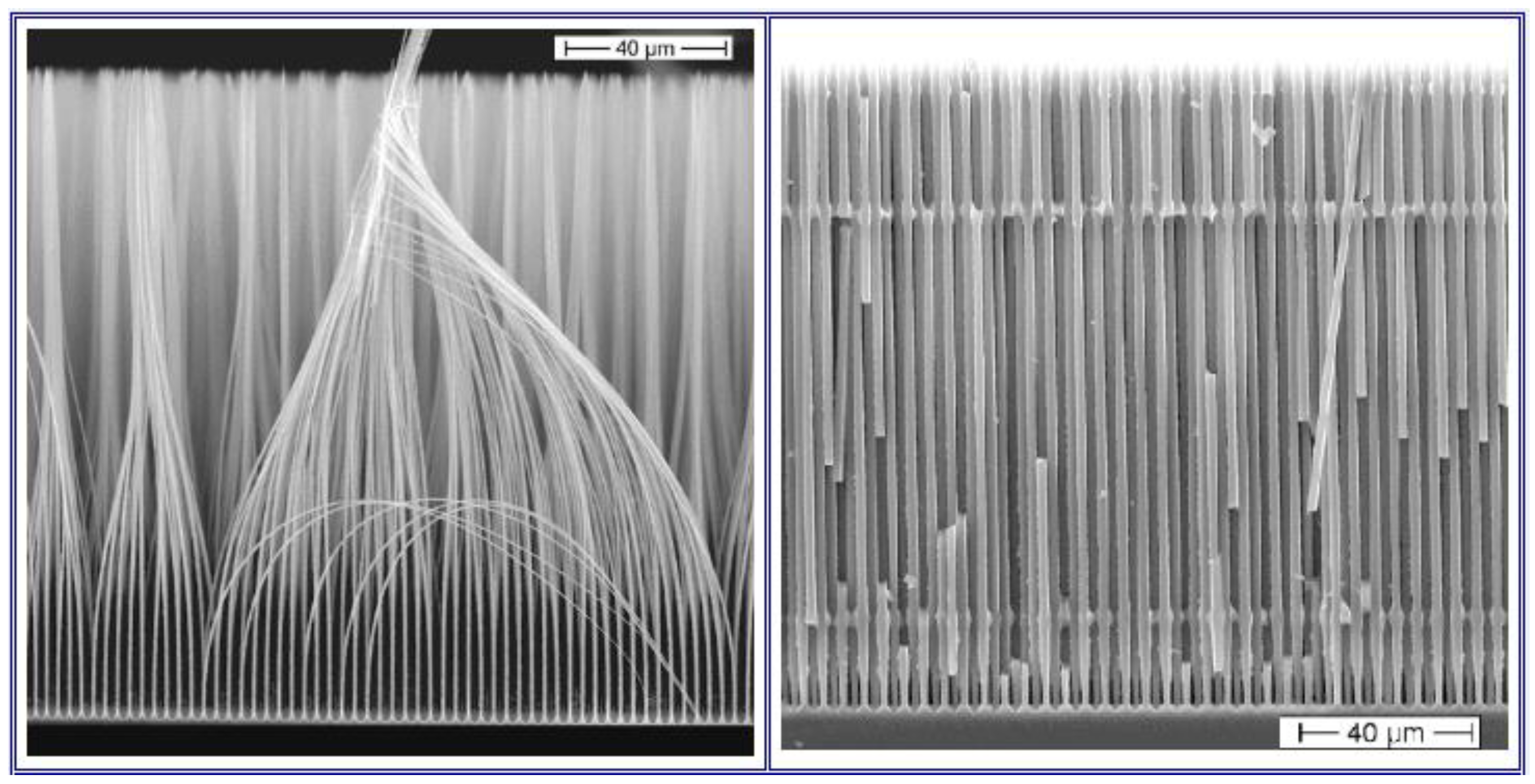
Figure 14.
Si "nanowires" made via electrochemical pore etching [161].
Figure 14.
Si "nanowires" made via electrochemical pore etching [161].
4.0. Semiconductor Manufacturing and Emerging Technologies
Semiconductor manufacturing involves crucial processes like wafer fabrication, doping, lithography, etching, and deposition (Figure 15) [167,168]. Various doping methods, such as ion implantation and diffusion, alter the electrical properties of semiconductors significantly. Lithography is essential for patterning at the nanometer scale, while etching allows for defining structures on the semiconductor surface. Deposition is a very vital process in adding thin films to the semiconductor substrate. Some of the new techniques that are evolving in the semiconductor manufacturing process include the use of plasma etching technology in flattening surfaces, as well as terminating the deposition of thin films at desired positions [167]. Additionally, advancements in semiconductor manufacturing involve addressing uncertainties and disturbances through control schemes like run-to-run control based on discrete active disturbance rejection control, which effectively suppresses disturbances and uncertainties in the manufacturing process [169]. These processes collectively contribute to the intricate and precise production of semiconductor devices in modern manufacturing environments [170].
4.1. Semiconductor Manufacturing Process
4.1.1. Wafer Fabrication
The foundation of semiconductor devices begins with wafer fabrication. First, a single crystal ingot like pure silicon is pulled and sliced into thin wafers. The wafers are polished to create a smooth surface. To analyze the defects such as stress fields in the crystal lattice, the wafer undergoes thermal treatments in which a radial temperature gradient acts on the wafer. This preparation is important because even minor defects will result in flaws in the final product. The wafers serve as the substrate for subsequent processing steps [171,172].
4.1.2. Doping
Doping is an essential process in semiconductor processing/manufacturing since it defines the electronic features of this material. Several methods are implemented to introduce impurities into semiconductor materials. These processes can change the resistivity, mobility, energy band gap, and light absorption coefficients [173]. Doping refers to introducing certain impurities into the wafer to alter its electrical properties. It can be done through a process of thermal diffusion or by ion implantation. Doping allows the creation of n-type and p-type semiconductors; this aspect is very important in forming p-n junctions that are basic to transistor operations [174].
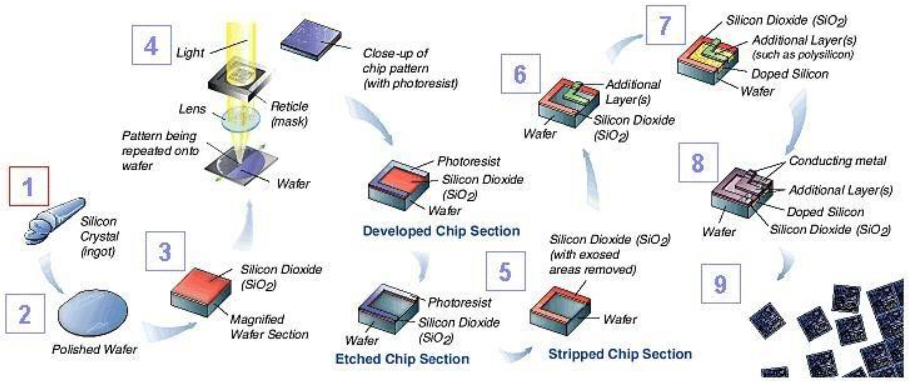
Figure 15.
Semiconductor Manufacturing Process Flowchart [175].
Figure 15.
Semiconductor Manufacturing Process Flowchart [175].
4.1.3. Thermal Oxidation
The thermal oxidation step in semiconductor manufacturing processes is a fundamental process for the creation of silicon dioxide layers on silicon wafers; these are integral components in most electronic devices [176,177]. This process helps in creating gate dielectrics, which are vital for the proper functioning of transistors and other semiconductor devices [177]. Optimized gas flow rate, oxidation time, and temperature in the thermal oxidation process guarantee that high-quality oxide layers are formed with the necessary thickness, which relates to semiconductor device performance and reliability [176]. Besides, it aids in reducing stress on wafers, enhances IC yield, and improves the quality of semiconductor products as a whole [178,179]. The precise control and optimization of the thermal oxidation process are essential for achieving high-quality semiconductor devices with optimal performance characteristics [180]. Thermal oxidation essentially involves the step of heating semiconductors on silicon wafers in an environment rich in oxygen at temperatures usually within the range of 800°C to 1200°C (Figure 16). It is within this temperature limit that the oxygen molecules diffuse into the silicon substrate and react to form silicon dioxide. There are two major techniques of thermal oxidation: Dry Oxidation and Wet Oxidation. Dry oxidation uses pure oxygen, and the oxide layer is thinner with higher quality (Si + O2 → SiO2).
They are characterized by slow growth, high density, and high breakdown voltage. Wet oxidation involves the use of steam, which may grow thicker oxide layers more quickly but of lesser quality compared with dry oxidation. Fast growth even at low temperatures is their characteristic feature and they permit thicker oxides [181].
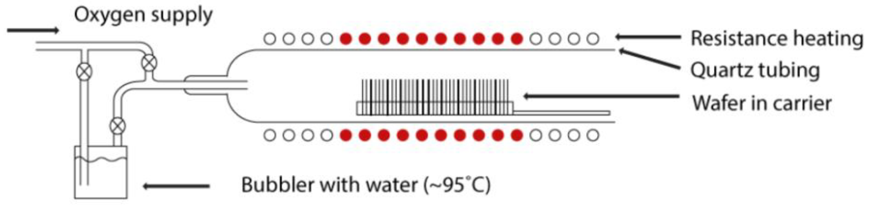
Figure 16.
Thermal Oxidation Schematic Drawing [182].
Figure 16.
Thermal Oxidation Schematic Drawing [182].
4.1.4. Lithography
Lithography is one of the most important patterning techniques in defining the geometric shapes of semiconductor devices on a substrate. After preparing the wafer, its surface is coated with a photoresist, a light-sensitive material that changes the chemical properties of the wafer to make it suitable for circuit printing [183]. There are two main types of photoresists based on their ultraviolet light (UV) reactivity: positive and negative. The positive photoresist becomes soluble upon exposure to UV light, and the exposed resist gets dissolved, leaving the unexposed resist remaining. On the other side, negative photoresists harden when exposed to UV light. Positive photoresist is more widely applied in the semiconductor manufacturing process due to its better thermal stability and resolution capability (Figure 17) [171].
The various steps in the photolithography process include the application of a layer of photoresist, coating with an adhesion promoter, pre and post-baking, light exposure, and finally the development of the exposed material. A photosensitive substance known as "photoresist" is applied to the wafer. Afterward, the photoresist-coated wafer is pre-baked from 90 to 120°C to fix the binding of the photoresist and evaporate the extra photoresist solvent. Then the photoresist is exposed to a pattern of intense light following the prebake. In optical lithography, UV light is commonly used. A post-exposure bake is conducted at 60 - 120°C to fix the pattern before development. There is then applied a developer to the photoresist layer. The substance can be such that it is able to dissolve either the irradiated or non-irradiated photoresist [184].
Photolithography refers to the process of drawing a circuit design onto a wafer. This is the step where the wafer is introduced to the photolithographic equipment and exposed to UV light. This light draws the pattern from the mask, containing the blueprint of the circuit, onto the wafer coated with a photoresist film. Using light, photolithography transfers a geometric pattern from a photomask onto the photoresist applied to a substrate. Variants of lithography include e-beam lithography, which uses a focused beam of electrons to create extremely fine patterns for small-scale devices, and extreme ultraviolet lithography (EUV), which uses EUV light to achieve smaller feature sizes essential for advanced semiconductor nodes. Refraction and defects can occur in the lithography process, which is why robust quality control is necessary. This is a critical step in defining the layout of electronic components, as well as creating complex patterns on the surface of the wafer [171,185].
4.1.5. Etching
After printing the circuit diagram on the wafer through lithography, the etching process follows to remove excess materials from the surface, creating the desired patterns (Figure 17). The two main primary types of etching include wet and dry etching. Wet etching involves chemical solutions that mostly dissolve material equally in all directions and are less precise. Dry etching, also known as plasma etching, uses ionized gases to remove the material and thus provides better resolution and anisotropy, which results in highly defined structures [171,172,185].
Emerging techniques like atomic layer etching (ALE) and cryogenic etching are critical in advanced semiconductor manufacturing. ALE provides atomic-level precision by alternating between etching and passivation steps, while cryogenic etching, performed at very low temperatures, enables the creation of high-aspect-ratio features with smooth sidewalls. These methods are of vital importance in advanced semiconductor devices. Semiconductors often require repeating the photolithography and etching processes several times on all layers of the wafer to achieve the final product; hence, precision is required, and close process control is necessary to prevent damage to the chip structure. Various methods in semiconductor processing, such as using atomized droplets with etching solutions at high temperatures, curing photoresists to reduce consumption, conducting multiple etch cycles with gas and purge gas introductions, and employing specific gas mixtures for plasma processing, aim to achieve precise and controlled material removal, enhancing efficiency and reducing costs [186,187].
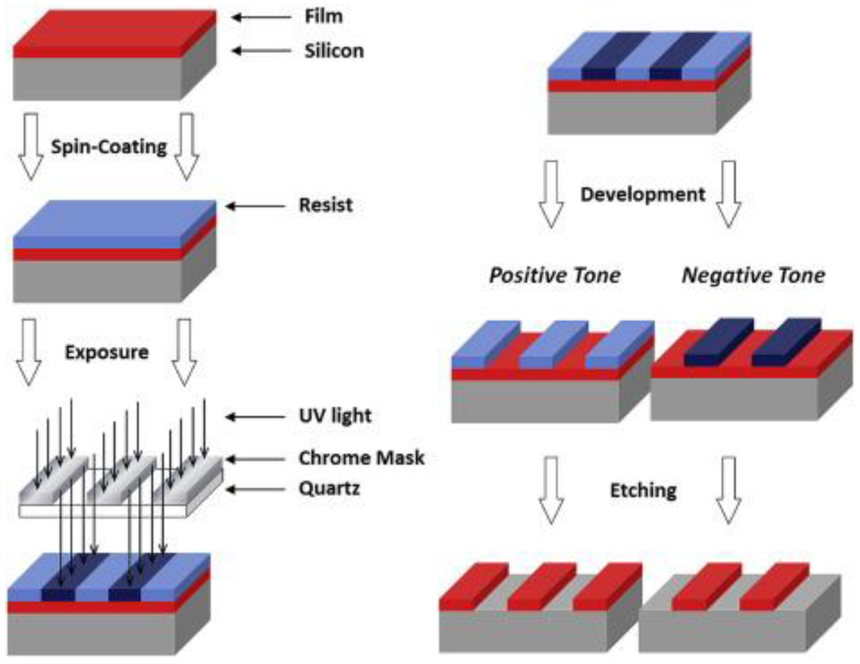
Figure 17.
The lithography and etching process [188].
Figure 17.
The lithography and etching process [188].
4.1.6. Deposition
Deposition involves adding thin films of materials onto the semiconductor substrate to form layers necessary for device functionality. Various techniques are used in this process including Chemical Vapor Deposition (CVD), Physical Vapor Deposition (PVD) and Atomic Layer Deposition. In chemical vapor deposition, chemical reactions in a vapor phase deposit materials onto the substrate. Variants of CVD include low-pressure CVD (LPCVD) and plasma-enhanced CVD (PECVD). Physical vapor deposition (PVD), which involves physical processes like sputtering or evaporation, is widely used for depositing metals. Another method, atomic layer deposition (ALD), deposits materials one atomic layer at a time, providing excellent control over thickness and uniformity. These deposited films serve multiple purposes, such as forming insulating layers, conducting paths, or active components like transistors [171,172,185].
4.1.7. Assembly and Packaging
The entire semiconductor manufacturing process (Figure 18) may take as long as 26 weeks from design to production. The last stage of the production process entails separating the wafer into individual chips (dicing) and placing the chips onto a substrate through bonding [190]. The key purposes of chip packaging focus on protecting individual chips from mechanical damage, providing a barrier against water and chemical impurities, ensuring the existence of strong links between each chip and an electrical circuit through the use of strong leads, and providing the means for chips to lose heat during its operation. Materials like plastic and ceramic are used to apply protective layers that encapsulate the chip, thereby preventing electric circuits from scoring or heat punctures [191]. After this process, the chip is ready for use.
The process of semiconductor manufacturing involves other steps, like testing and inspecting chips. Among the most common problems that create issues for manufacturers are:
Product Quality; The difficulty in ensuring quality products can arise as semiconductor products become more sophisticated and their demand increases. Defects; There are several steps from assembling to testing that can lead to defects in the products. These defects can hardly be noticed considering the size of each chip and the number of its layers. Cost; The cost associated with the semiconductor manufacturing process continues to rise, with new technologies coming out and shortages occurring that make it harder for manufacturers to break even in revenue. Equipment; Advances within the industry will require manufacturers to keep pace with new equipment and technologies, which can be a struggle and an added cost. Time; Even minor production faults render hundreds of chips useless, and there is almost always a challenge of minimizing the downtime in case of quality compromise and delay [171].
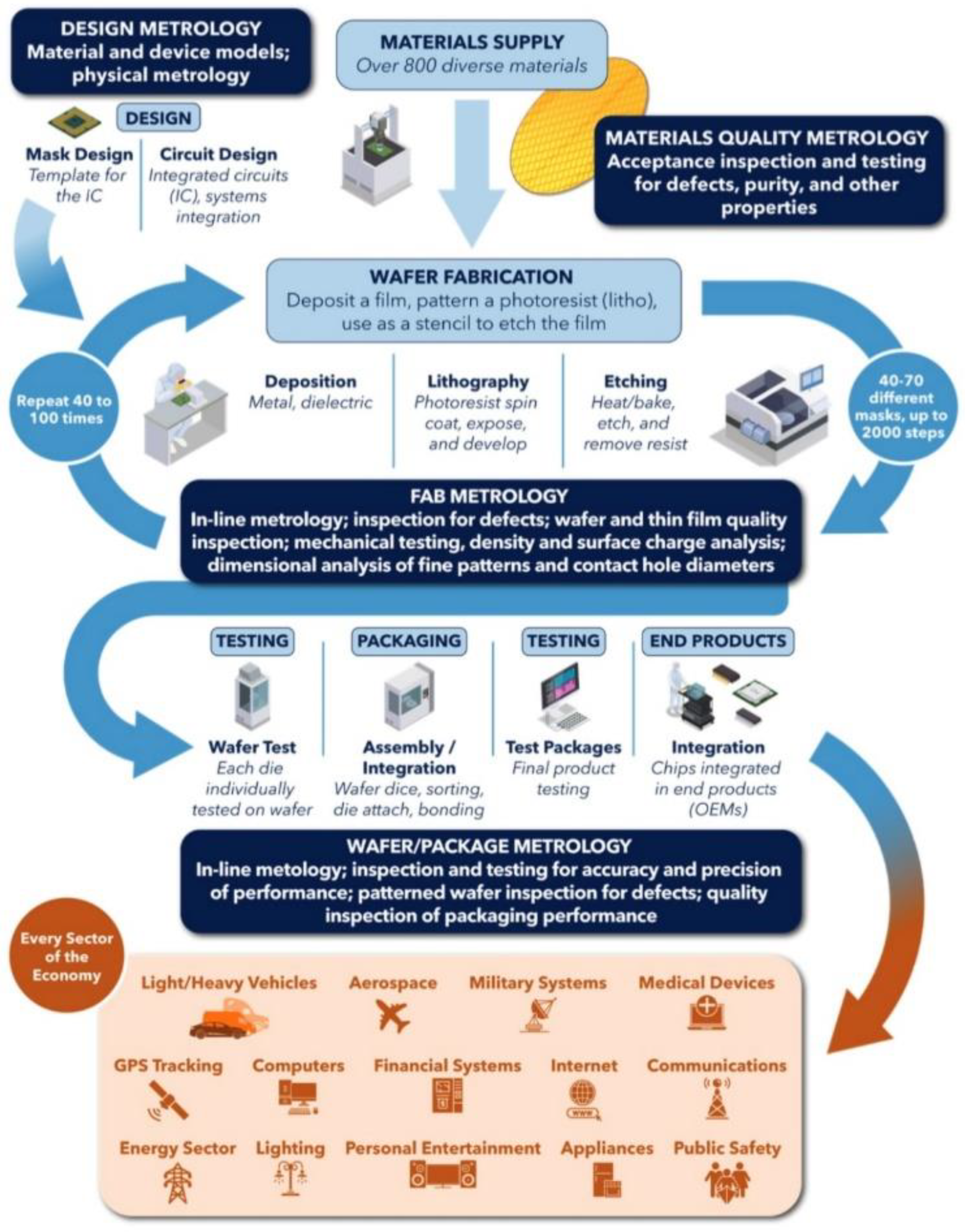
Figure 18.
A comprehensive overview of the semiconductor fabrication process, detailing the steps from materials supply and wafer fabrication to testing and integration. The diagram highlights the critical role of metrology in ensuring quality and precision at each stage, from design through to end products utilized across various sectors of the economy [189].
4.2. Emerging Techniques in Semiconductor Manufacturing
As the semiconductor industry evolves, several emerging techniques are gaining traction.
Extreme Ultraviolet Lithography (EUV); The technique under modern lithography uses shorter wavelengths of light to create smaller features on chips, underlying more powerful, more efficient devices on the market. Compared to conventional optical lithography, this technique uses a shorter wavelength of light, 13.5 nm. This allows for smaller features to be carried on chips, enabling the production of devices that are more powerful and efficient. EUV lithography has the potential to overcome the limitations of optical lithography, which is getting to the end of its resolution, and to make it possible to manufacture features in the sub-10 nm scale. [192].
Atomic Layer Deposition (ALD); Atomic layer deposition (ALD) is a thin film deposition technique that allows for the precise control of film thickness at the atomic level. This is particularly important as the devices shrink in size, as it enables the fabrication of ultra-thin and conformal films [193,194]. ALD exposes the substrate to alternating gaseous precursors that react with the surface to deposit a layer of atoms one at a time. This method offers superb control of film thickness, composition, and conformality, making it an essential process for advanced semiconductor manufacturing.
3D Integration; 3D integration revolutionizes the semiconductor industry by stacking circuits vertically, enabling higher performance and reduced device footprint. Through-silicon vias (TSVs) or Cu-Cu connections are utilized for interconnecting stacked layers, facilitating shorter interconnects and increased integration density [195]. This technique allows for heterogeneous integration, where diverse components fabricated using optimized processes can be stacked together, enhancing overall performance and functionality [196]. The integration of various technologies like analog, radio frequency, sensors, memory devices, and digital components in a vertically stacked manner opens up possibilities for improved communication bandwidth, design flexibility, and cost reduction, aligning with the "More than Moore" paradigm in semiconductor advancements [197].
5.0. Innovation and Future Prospect
The present trends in the semiconductor industry are oriented toward modernization at a very high rate. Major areas of focus remain quantum semiconductors, flexible electronics, and miniaturization technologies. [198,199,200]. These new cutting-edge developments are pushing this industry toward more efficient and cost-effective solutions, especially in the context of emerging applications like autonomous vehicles and energy-efficient chips [198]. The future roadmap of the industry is forecasted to be one of low power consumption, low e-waste generation, and alternative raw materials to respond to market demand and regulatory policy [198]. What is more, the semiconductor industry being an emerging market can be proved from the aspect that the sale of electronic goods will boost up to $1 trillion by 2030, indicating the huge space for development and technology development in this industry [201]. This underlines the critical role semiconductors play in driving economic growth, national security, and technological innovation, which supports continued research and development efforts to ensure leadership in microelectronics manufacturing and a sustainable future for the industry as a whole [189].
Recent strides made in the semiconductor industry have greatly innovated flexible electronics, quantum semiconductors, and miniaturization. Developments like these are changing the face of electronic devices, opening up possibilities for technologies of the future.
Flexible electronics, otherwise known as flex circuits, are a technology where the mounting of electronic devices is done on flexible plastic substrates. This feature brings along several advantages over their traditional counterpart, rigid electronics, which include flexibility and durability. They are bendable, foldable, and even rollable without sustaining any damage; hence, they are highly applicable where space is limited or, inversely, flexibility is very essential. They are resistant to some tough environmental conditions and suffer less mechanical damage. Applications of flexible electronics include flexible displays, RFID tags, flexible sensors, and memories. They find special applications in those areas where traditional devices are hard to apply, like wearable devices, medical implants, and automotive systems [202,203].
Quantum semiconductors, which harness the principles of quantum mechanics, are about to revolutionize the semiconductor industry. Quantum computing, for example, uses quantum bits qubits, which can be in a superposition, thus enabling one qubit to process multiple information bits simultaneously. This increases the speed of processing of certain types of tasks exponentially. Technologies like these have enormous potential for performance enhancement and could change industries. Quantum computers can solve complex problems much faster than classical computers; therefore, they would be suitable for applications such as cryptography, artificial intelligence, and simulation of complex systems. Quantum computing has the potential to be huge in epidemiology, cryptography, machine learning, and data analysis due to its power to enhance capabilities and efficiency [204,205,206,207].
Miniaturization; This miniaturization of semiconductors has been behind the advancement of modern electronics. The progress emanates from Moore’s Law, which has facilitated the development of small and highly efficient gadgets. Key among these developments is Deep Submicron Technology. Other techniques, such as lithography and etching, have made it possible to create semiconductor devices in the submicron regime, increasing their performance and efficiency. Fin Field-Effect Transistors came to introduce better performance and reduce leakage in nano-scale devices.
Advanced lithography technique such as Extreme Ultraviolet Lithography uses shorter wavelengths to create even smaller features, thus essential in manufacturing advanced nano-scale semiconductors [208].
6.0. Opportunity and Areas of Expansion
Semiconductors present vast opportunities for growth and impact across various sectors such as renewable energy, healthcare, and telecommunications. In terms of growth, the sector is already witnessing high growth and diversification, contributed by rapid technological progress and growing demand from different industries (Figure 19) [200].
One major area of development in this regard has been playing out with the role of artificial intelligence within this semiconductor landscape. The AI-related semiconductor market was expected to grow from $6 billion in 2020 to over $30 billion in 2022, representing compound annual growth (CAGR) of nearly 50% [209] in less than three years alone. The high demand from AI for advanced processing capability will drive growth in microprocessors and memory chips and hence become a key area for investment and development. Moreover, the application of AI technologies in semiconductor manufacturing processes—product development, risk assessment, and defect classification—has taken a different route with the intervention of deep learning and machine learning techniques, further propelling the industry [210].
The automotive sector has also remained a dominant driver of semiconductor demand, especially with increasing electric vehicles (EVs) and advanced driver-assistance systems (ADAS). The outlook of the automotive semiconductor market is encouraging, with the CAGR for ADAS calculated at nearly 20% by 2027 [211]. Indeed, the need for semiconductors is probably going to increase due to the increasing digitization of vehicles powered by complex electronics. By design, according to this, energy-efficient chips and manufacturing processes can power autonomous cars and vehicles [210]. Moreover, semiconductors are at the heart of innovations in high-performance computing, wireless connectivity, and autonomous driving, thereby contributing to productivity, efficiency, safety, and sustainability.
The rollout of 5G technology is creating large opportunities for semiconductor manufacturers. With faster and more efficient communication devices requiring advanced chipsets, this has increased their demand, especially those chipsets designed for Internet of Things applications. The integration of IoT and AI into telecommunications is expected to drive further growth in this sector [212,213]. The convergence will come up with some of the cutting-edge technologies and improve communication infrastructure, thus strengthening the role of semiconductors in modern telecommunications.
Semiconductors drive most of the renewable energy technologies, from solar inverters to energy management systems. As the world is moving into sustainable energy, the demand for semiconductors that facilitate the process of energy conversion and storage will rise. This opens up huge opportunities for companies to innovate and widen product lines in this field. Another solution would be the progress in material research that can be done to make semiconductors relatively cheap and more effective. It would be realized through the development of energy-efficient chips and manufacturing processes [214].
Healthcare is increasingly being driven by semiconductor technology that is powering medical devices, diagnostics tools, and telehealth solutions. Increased patient monitoring, data collection, and analysis within healthcare devices pertaining to the domains of AI and IoT open new fields of device application and correlated semiconductors. This trend supports the market growth of semiconductors in healthcare delivery improvement and better patient outcomes [212,213].
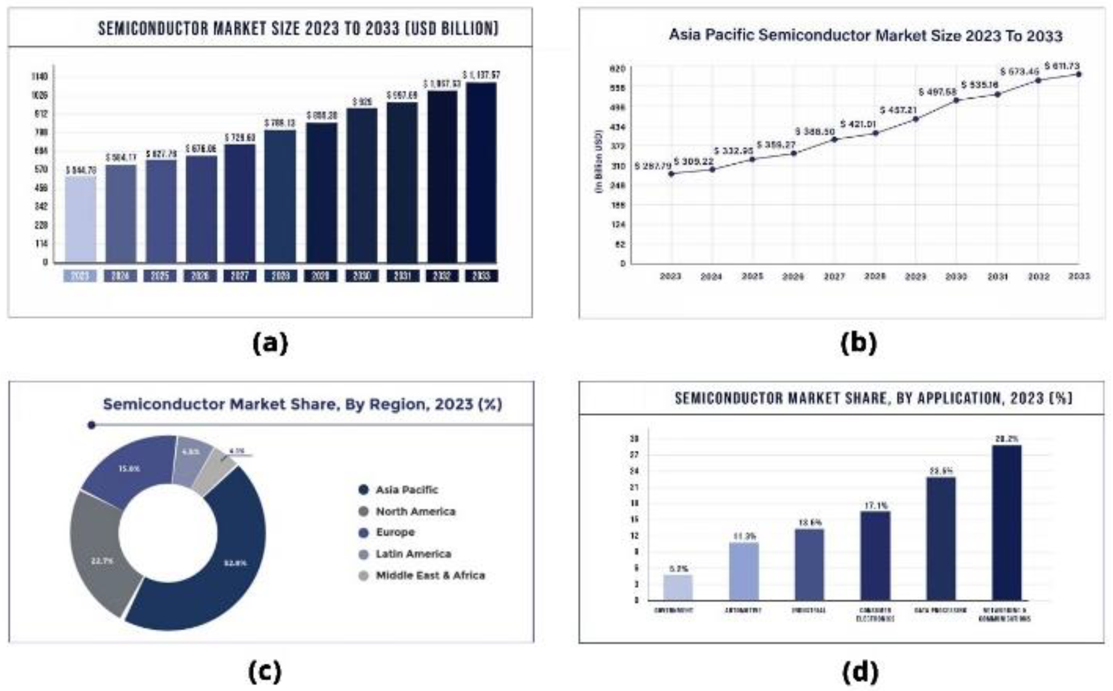
Figure 19.
(a) Projected Global Semiconductor Market Size from 2023 to 2033 (USD Billion). The market is expected to grow from $544.78 billion in 2023 to $1,137.57 billion in 2033. (b) Projected Semiconductor Market Size in the Asia Pacific Region from 2023 to 2033 (USD Billion). The market is anticipated to increase from $287.79 billion in 2023 to $611.73 billion in 2033. (c) Semiconductor Market Share by Region in 2023 (%). The Asia Pacific region leads with 52.8%, followed by North America (22.7%), Europe (15.8%), Latin America (4.5%), and the Middle East & Africa (4.1%). (d) Semiconductor Market Share by Application in 2023 (%). The largest share is held by Networking & Communications (29.2%), followed by Data Processing (23.6%), Consumer Electronics (17.1%), Industrial (13.6%), Automotive (11.3%), and Government (5.2%) [213].
Geopolitical dynamics are reshaping the semiconductor industry given the increasingly important role that manufacturing plays in ensuring both national security and economic stability. Government incentives become a leading force in expanding companies to new regions, especially for greenfield investments where the focus is both sustainability and supply chain security. This development sets the stage for companies to do business in locations away from traditional strongholds of the semiconductor industry, therefore engendering a more diversified and resilient global semiconductor supply chain [214].
Sustainability and supply chain resilience are very slowly becoming a trend in semiconductors. Environmentally friendly practices, coupled with the new need to be supply chain resilient, have been incorporated into the long-term growth strategy by various companies. Such focus on sustainability is expected to shape decisions related to manufacturing locations and partnerships into a more sustainable and resilient industry [213,214].
The semiconductor industry faces a talent shortage. It has therefore been exposed to be the imperative of workforce development. Firms have to invest in a skilled workforce through the delivery of training and retention programs to ensure that skilled workers are geared up for increasing sector demand. This ’talent-oriented’ approach will be critical to staying competitive and driving innovation while maintaining the growth momentum of the industry (Figure 19 [211].
The future of the semiconductor industry is therefore niche in innovating and adapting. It makes possible the advancement in the most critical sector.
7.0. Sustainability and SDG Alignment
The semiconductor industry underpins sustainable development and achievement of the United Nations SDGs. Given the constantly growing demand for semiconductors to match strides in technology and transition to a low-carbon economy, the industry must adopt practices that promote energy efficiency, waste reduction, and the use of eco-friendly materials [215,216].
Semiconductors are integral to numerous applications that enhance energy efficiency, particularly in the context of SDG 7, which focuses on ensuring access to affordable, reliable, sustainable, and modern energy for all. Research shows a significant focus on SDG 7 (Affordable and Clean Energy), accounting for 68.9% of semiconductor-related SDG publications from 2017 to 2022 (Figure 20) [217]. This calls for inventions like low-power chips and energy-efficient designs to save the general energy consumption of the devices. The industry is working on complex manufacturing challenges with data-driven approaches, coupled with advanced modeling techniques, to allow more sustainable practices [218]. Universities contribute to SDG 7 by promoting energy sustainability and efficiency through research and knowledge transmission [219].
The Semiconductor Climate Consortium, founded in 2022, marks the industrywide push to increase energy efficiency and reduce emissions throughout the semiconductor life cycle. This collaborative approach aims to meet the Paris Agreement Goals by fostering standards and practices that lower energy use in semiconductor manufacturing and application [220]. Product design has increasingly included energy efficiency as a prime criterion, and companies have been optimizing power, performance, and area (PPA) to make chips not only become better performers but also be frugal with their power consumption—thereby reducing lifetime emissions and operational cost [220,221].
The semiconductor industry faces significant challenges regarding waste generation and resource use, which are critical to achieving SDG 12: Responsible Consumption and Production. Closed-loop manufacturing processes can facilitate the recycling and reuse of materials within the semiconductor production cycle. This approach minimizes waste and reduces the reliance on raw material extraction, aligning with circular economy principles [222]. The development of efficient recycling methods and the exploration of biodegradable materials are essential for mitigating the environmental impact of electronic waste. Research is ongoing in the development of semiconductor components that can be easily repaired, refurbished, or recycled to extend their lifecycle and reduce landfill contributions [221,222].
The transition to sustainable materials is vital for the semiconductor industry to align with SDG 9, which emphasizes building resilient infrastructure, promoting inclusive and sustainable industrialization, and fostering innovation. Focus is also placed on the development of new materials that are recyclable or biodegradable. This ranges from research into plant-based polymers and other sustainable alternatives that can replace traditional semiconductor materials to reduce environmental impact during production and upon disposal [220,221]. Many semiconductor manufacturers are committing to the use of renewable energy sources in their operations. Companies like Intel and TSMC are driving this shift, having set targets to source a large part of their energy from renewable sources by 2030 to reduce carbon emissions and thereby aid in the global transition to sustainable energy [222,223].
Sustainable practices in related sectors, such as construction, also align with multiple SDGs, including SDG 7, SDG 9 (Industry, Innovation, and Infrastructure), and SDG 11 (Sustainable Cities and Communities) [224]. However, there is a need for increased collaboration between academia and industry to amplify the impact of semiconductor innovations on the SDGs [217]. Semiconductor companies are actively working towards reducing energy consumption and waste through initiatives like developing low-power chips and utilizing recyclable materials, thus contributing to SDG targets such as affordable and clean energy, responsible consumption, and industry innovation. This focus on energy efficiency, waste reduction, and eco-friendly materials reflects a broader trend across industries towards sustainable practices, emphasizing the importance of technological advancements in achieving environmental and social objectives. Additionally, the engagement of multinational corporations (MNCs) in sustainable development programs further underscores the significance of semiconductor companies’ efforts in addressing global challenges and promoting positive externalities [216].
Figure 20.
(a) Number of semiconductor-related publications from 2017 to 2022 by SDG program. (b) Number of SDG-related publications on semiconductors per year from 2017 to 2022. (c) Countries contributing to SDG 7-related publications from 2017 -2022 [217].
Figure 20.
(a) Number of semiconductor-related publications from 2017 to 2022 by SDG program. (b) Number of SDG-related publications on semiconductors per year from 2017 to 2022. (c) Countries contributing to SDG 7-related publications from 2017 -2022 [217].
8.0. Conclusions
The future of semiconductor technologies is replete with potential and innovation. Technologies that form the basis for most modern electronics have continually been evolving to bring new solutions to contemporary challenges in energy efficiency, computational power, and sustainability. This review underlines important key advancements in semiconductor materials and processes, underscoring those sustainable practices will play a critical role in the future of the industry. By integrating cutting-edge innovations with environmental consciousness, the semiconductor industry can lead the way toward a more sustainable technological future. Green technologies must hold priority in future research and development for the progress in the semiconductor technologies ahead. There is much hope in the future journey with several opportunities for growth and development in both established and emerging applications.
Author Contributions
The manuscript was written through contributions of all authors. All authors have approved the final version of the manuscript.
Data Availability Statement
No data was used for the research described in the article.
Conflicts of Interest
The authors declare that they have no known competing financial interests or personal relationships that could have appeared to influence the work reported in this paper.
References
- B. G. Streetman, “Solid state electronic devices,” p. 463, 1972.
- Z. Qiu, X. Shen, and Z. Zhao, “Development Trends and Prospects of Semiconductor Devices and Technology,” 2024. [CrossRef]
- F. Junior, C. Nunes, P. E. Redkva, and B. Sandrino, “Semiconductors In The Digital Age: Evolution, Challenges, And Geopolitical Implications,” vol. 12, pp. 133–150, 2023, doi: 10.32749/nucleodoconhecimento.com.br/technology. [CrossRef]
- M. Schroter et al., “The EU DOTSEVEN Project: Overview and Results,” Technical Digest - IEEE Compound Semiconductor Integrated Circuit Symposium, CSIC, vol. 2016-November, Nov. 2016, doi: 10.1109/CSICS.2016.7751070. [CrossRef]
- R. Venkatesh, Dr. S. Selvakumar, S. Dhasneem, and L. V. Kannan, “SEMICONDUCTOR DEVICES: AN OVERVIEW,” Futuristic Trends in Electrical Engineering Volume 3 Book 1, pp. 11–37, Jun. 2024, doi: 10.58532/V3BDEE1P2CH1. [CrossRef]
- S. Roy, C. Kumar Ghosh, S. Dey, and A. Kumar Pal, “Solid State & Microelectronics Technology,” Solid State & Microelectronics Technology, Jun. 2023, doi: 10.2174/97898150798761230101. [CrossRef]
- B. D. Fahlman, “Semiconductors,” Materials Chemistry, pp. 291–405, 2023, doi: 10.1007/978-3-031-18784-1_4. [CrossRef]
- D. Sweidan, “The geopolitics of technology: Evidence from the interaction between the United States and China,” Russian Journal of Economics 10(2): 130-150, vol. 10, no. 2, pp. 130–150, Jul. 2024, doi: 10.32609/J.RUJE.10.118505. [CrossRef]
- S. Kumar, “Semiconductor Geopolitics - Past, Present, and Future,” Indian Public Policy Review, vol. 5, no. 1 (Jan-Feb), pp. 171–174, Feb. 2024, doi: 10.55763/IPPR.2024.05.01.005. [CrossRef]
- Rodrigo and V. Velasco, “Neo-Mercantilism in The Semiconductor Industry: The Chinese Strategy,” 2024. [Online]. Available: https://ajesh.ph/index.php/gp. [CrossRef]
- Q. Bu, “Can de-risking avert supply chain precarity in the face of China-U.S. geopolitical tensions? From sanctions to semiconductor resilience and national security,” International Cybersecurity Law Review 2024 5:3, vol. 5, no. 3, pp. 413–442, Jun. 2024, doi: 10.1365/S43439-024-00125-1. [CrossRef]
- J. Germann, S. Rolf, J. Baines, and S. K. Starrs, “A Chip War Made in Germany? US Techno-Dependencies, China Chokepoints, and the German Semiconductor Industry,” Politics and Governance, vol. 12, no. 0, p. 8265, Jul. 2024, doi: 10.17645/PAG.8265. [CrossRef]
- S. Suresh, “Semiconductor Nanomaterials, Methods and Applications: A Review,” Nanoscience and Nanotechnology, 2013. [CrossRef]
- A. Wilson, “The Theory of Electronic Semi-Conductors,” Proceedings of The Royal Society A: Mathematical, Physical and Engineering Sciences, vol. 133, no. 822, pp. 458–491, Oct. 1931, doi: 10.1098/RSPA.1931.0162. [CrossRef]
- C. D. Vedel, E. Brugnolotto, S. Smidstrup, and V. P. Georgiev, “Impact of different types of planar defects on current transport in Indium Phosphide (InP),” in 2021 Joint International EUROSOI Workshop and International Conference on Ultimate Integration on Silicon, EuroSOI-ULIS 2021, Institute of Electrical and Electronics Engineers Inc., Sep. 2021. doi: 10.1109/EuroSOI-ULIS53016.2021.9560698. [CrossRef]
- T. E. of E. Britannica, “Semiconductor,” Britannica. Jul. 01, 2024. Accessed: Jul. 23, 2024. [Online]. Available: https://www.britannica.com/science/semiconductor.
- A. Zola, “What Is a Semiconductor and What Is It Used for?,” TechTarget. Accessed: Jul. 23, 2024. [Online]. Available: https://www.techtarget.com/whatis/definition/semiconductor.
- Aakash BYJU’S, “Semiconductors - Types, Examples, Properties, Application and Uses,” BYJU’S. Accessed: Jul. 23, 2024. [Online]. Available: https://byjus.com/jee/semiconductors/.
- O. Madelung, “Semiconductors: Data Handbook,” Semiconductors: Data Handbook, 2004, doi: 10.1007/978-3-642-18865-7. [CrossRef]
- A. Ayodele, “What is a Semiconductor? A Comprehensive Guide to Engineering Principles and Applications,” Wevolver. Accessed: Jul. 23, 2024. [Online]. Available: https://www.wevolver.com/article/what-is-a-semiconductor-a-comprehensive-guide-to-engineering-principles-and-applications.
- N. Williams and M. O’kane, “Semiconductors: How Do They Work?,” Ossila. Accessed: Jul. 23, 2024. [Online]. Available: https://www.ossila.com/pages/how-semiconductors-work.
- GreeksforGreeks, “Semiconductors,” GreeksforGreeks. Accessed: Jul. 23, 2024. [Online]. Available: https://www.geeksforgeeks.org/semiconductors/.
- S. Das, “How Semiconductor Works,” Electronics Tutorial. Accessed: Jul. 23, 2024. [Online]. Available: https://www.electronicsandyou.com/blog/how-semiconductor-works.html.
- A. D. Terna, E. E. Elemike, J. I. Mbonu, O. E. Osafile, and R. O. Ezeani, “The future of semiconductors nanoparticles: Synthesis, properties and applications,” Materials Science and Engineering: B, vol. 272, p. 115363, Oct. 2021, doi: 10.1016/J.MSEB.2021.115363. [CrossRef]
- L. Łukasiak and A. Jakubowski, “History of Semiconductors,” Journal of Telecommunications and Information Technology, no. 1, pp. 3–9, Mar. 2010, doi: 10.26636/jtit.2010.1.1015. [CrossRef]
- P. Bisimide, Y. Nagai, T. Watanabe, and D. Yoshioka, “Early history of the physics and chemistry of semiconductors-from doubts to fact in a hundred years You may also like Near-Infrared-Light Triggered Electron Transfer from Ag 2 S Nanocrystals to,” 1989. [CrossRef]
- W. F. Brinkman, D. E. Haggan, and W. W. Troutman, “A History of the Invention of the Transistor and Where It Will Lead Us,” 1997. [CrossRef]
- P. Russer, Ferdinand Braun — A pioneer in wireless technology and electronics. 2009. doi: 10.23919/EUMC.2009.5296324. [CrossRef]
- A. S. Lather, “Study of Semiconductor Devices,” Universal Research Reports, vol. 4, no. 4, pp. 32–34, Sep. 2017, Accessed: Jul. 29, 2024. [Online]. Available: https://urr.shodhsagar.com/index.php/j/article/view/148.
- “143149b0”.
- G. Zorpette, “The Ripples From Edwin Hall’s Effect How a 143-year-old insight is shaping spacecraft propulsion,” 1922. [CrossRef]
- Z. Jia, “Léon Brillouin and the Brillouin Zone,” Semantic Scholar, 2018.
- G. Bhattacharya and A. Venimadhav, “An alternative approach to extract diode parameters from metal-semiconductor-metal asymmetric Schottky diodes,” J Phys D Appl Phys, vol. 55, no. 43, Oct. 2022, doi: 10.1088/1361-6463/ac85ff. [CrossRef]
- K. Dilshad and M. K. Rabinal, “Experiment with Schottky junction: Estimation of metal-semiconductor interface parameters,” Eur J Phys, vol. 40, no. 3, Apr. 2019, doi: 10.1088/1361-6404/ab080f. [CrossRef]
- Calif. Nanotechnology Conference and Trade Show 2005 Anaheim et al., Workshop on Compact Modeling. NSTI, 2005.
- L. Khiangte, R. S. Dhar, K. Kumar, and J. L. Pachuau, “State-of-the-art MOSFET and TCAD in the advancement of technology: A review,” 2018.
- H. R. Huff, “John Bardeen and transistor physics,” AIP Publishing, Feb. 2003, pp. 3–32. doi: 10.1063/1.1354371. [CrossRef]
- H. Iwai and D. Misra, “The Transistor was Invented 75 Years Ago: A Big Milestone in Human History,” Electrochemical Society Interface, vol. 31, no. 4, pp. 65–72, Dec. 2022, doi: 10.1149/2.F13224IF/XML. [CrossRef]
- J. Binbin and S. Chihtang, “The Complete Semiconductor Transistor,” Dec. 25, 2009, IEEE, Gainesville, Florida, USA. [CrossRef]
- Y. Zhang, “MOSFET amplifier circuits,” The Tao of Microelectronics, 2014, doi: 10.1088/BK978-1-6270-5453-9CH4. [CrossRef]
- T. H. Lee, “The Design of CMOS Radio-Frequency Integrated Circuits: A REVIEW OF MOS DEVICE PHYSICS,” The Design of CMOS Radio-Frequency Integrated Circuits, pp. 167–201, Jun. 2003, doi: 10.1017/CBO9780511817281.007. [CrossRef]
- “235206332”.
- C. Phipps, “Jack S. Kilby,” Semantic Scholar, Dec. 2007, Accessed: Jul. 20, 2024. [Online]. Available: https://www.semanticscholar.org/paper/Jack-S.-Kilby-Phipps/178b0a87d4beb93c67bc77a8ec06d939d425176d.
- C. C. M. Mody, “The little-known history of Jack Kilby’s misadventure in solar power,” IEEE Spectr, vol. 53, no. 10, pp. 50–55, Oct. 2016, doi: 10.1109/MSPEC.2016.7572539. [CrossRef]
- H. R. Schroeder, “The Man Behind the Microchip: Robert Noyce and the Invention of Silicon Valley [Book Review],” IEEE Technology and Society Magazine, vol. 25, no. 3, pp. 50–51, Autumn 2006, doi: 10.1109/MTAS.2006.1700022. [CrossRef]
- L. Berlin, “The Man behind the Microchip: Robert Noyce and the Invention of Silicon Valley,” The Man behind the Microchip: Robert Noyce and the Invention of Silicon Valley, pp. 1–440, Sep. 2007, doi: 10.1093/ACPROF:OSO/9780195163438.001.0001. [CrossRef]
- P. B. Ghate, “Interconnections in VLSI,” Phys Today, vol. 39, no. 10, pp. 58–66, Oct. 1986, doi: 10.1063/1.881069. [CrossRef]
- R. Doering, “50 Years of ``Scaling’’ Jack Kilby’s Invention,” Bulletin of the American Physical Society, 2008.
- R. Noyce’s, D. Alberti, and M. Amoroso, “The Back Story: Finding Noyce’s Notebook,” IEEE Spectr, vol. 42, no. 5, p. 7, 2005, doi: 10.1109/MSPEC.2005.1426955. [CrossRef]
- R. Teja, “Tunnel Diode - Working, Characteristics, Application,” ElectronicsHub. Accessed: Jul. 25, 2024. [Online]. Available: https://www.electronicshub.org/tunnel-diode-working-characteristics-applications/.
- A. Varshney, W. Yan, and P. Dutta, “Judo: Addressing the Energy Asymmetry of Wireless Embedded Systems through Tunnel Diode based Wireless Transmitters,” in MobiSys 2022 - Proceedings of the 2022 20th Annual International Conference on Mobile Systems, Applications and Services, Association for Computing Machinery, Inc, Jun. 2022, pp. 273–286. doi: 10.1145/3498361.3538923. [CrossRef]
- L. Berlin and H. C. Casey, “Robert Noyce and the tunnel diode,” IEEE Spectr, vol. 42, no. 5, pp. 49–53, 2005, doi: 10.1109/MSPEC.2005.1426971. [CrossRef]
- H. Xiao, Y. Tian, X. An, R. Huang, and Y. Wang, “Quasi-SOI MOSFET: a novel architecture combining the advantages of SOI and bulk devices,” Semicond Sci Technol, vol. 20, no. 9, p. 925, Aug. 2005, doi: 10.1088/0268-1242/20/9/007. [CrossRef]
- S. Verma MTech Scholor SISTEC and B. Mohd Abdullah Assistant Professor SISTEC, “Review of SOI MOSFET Design and Fabrication Parameters and its Electrical Characteristics,” 2015.
- G. C. Patil and S. Qureshi, “Engineering spacers in dopant-segregated Schottky barrier SOI MOSFET for nanoscale CMOS logic circuits,” Semicond Sci Technol, vol. 27, no. 4, p. 045004, Feb. 2012, doi: 10.1088/0268-1242/27/4/045004. [CrossRef]
- R. Huang et al., “Novel Localized-SOI MOSFET’s Combining the Advantages of SOI and Bulk Substrates for Highly-Scaled Devices,” International Conference on Electron Devices and Solid-State Circuits, pp. 81–86, 2005, doi: 10.1109/EDSSC.2005.1635211. [CrossRef]
- H. Xiao, Y. Tian, X. An, R. Huang, and Y. Wang, “Quasi-SOI MOSFET: a novel architecture combining the advantages of SOI and bulk devices,” Semicond Sci Technol, vol. 20, no. 9, p. 925, Aug. 2005, doi: 10.1088/0268-1242/20/9/007. [CrossRef]
- G. C. Patil and S. Qureshi, “Engineering spacers in dopant-segregated Schottky barrier SOI MOSFET for nanoscale CMOS logic circuits,” Semicond Sci Technol, vol. 27, no. 4, p. 045004, Feb. 2012, doi: 10.1088/0268-1242/27/4/045004. [CrossRef]
- G. C. Patil and S. Qureshi, “A novel δ-doped partially insulated dopant-segregated Schottky barrier SOI MOSFET for analog/RF applications,” Semicond Sci Technol, vol. 26, no. 8, p. 085002, Apr. 2011, doi: 10.1088/0268-1242/26/8/085002. [CrossRef]
- G. C. Patil and S. Qureshi, “Impact of Segregation Layer on Scalability and Analog/RF Performance of Nanoscale Schottky Barrier SOI MOSFET,” JOURNAL OF SEMICONDUCTOR TECHNOLOGY AND SCIENCE, vol. 12, no. 1, pp. 66–74, 2012, Accessed: Jul. 20, 2024. [Online]. Available: https://www.dbpia.co.kr/journal/articleDetail?nodeId=NODE01820214.
- S. Matsumoto et al., “Study on the device characteristics of a quasi-SOI power MOSFET fabricated by reversed silicon wafer direct bonding,” IEEE Trans Electron Devices, vol. 45, no. 9, pp. 1940–1945, 1998, doi: 10.1109/16.711359. [CrossRef]
- Y. Cheng, M. J. Deen, and C. H. Chen, “MOSFET modeling for RF IC design,” Electron Devices, IEEE Transactions on Devices, vol. 52, no. 7, pp. 1286–1303, Jul. 2005, doi: 10.1109/TED.2005.850656. [CrossRef]
- M. Östling, J. Luo, V. Gudmundsson, P. E. Hellström, and B. G. Malm, “Nanoscaling of MOSFETs and the implementation of Schottky barrier S/D contacts,” 2010 27th International Conference on Microelectronics, MIEL 2010 - Proceedings, pp. 9–13, 2010, doi: 10.1109/MIEL.2010.5490540. [CrossRef]
- K. Sivasankaran and P. S. Mallick, “Multigate Transistors for High Frequency Applications,” 2023, doi: 10.1007/978-981-99-0157-9. [CrossRef]
- K. O. Petrosyants, D. S. Silkin, and D. A. Popov, “Comparative Characterization of NWFET and FinFET Transistor Structures Using TCAD Modeling,” Micromachines (Basel), vol. 13, no. 8, Aug. 2022, doi: 10.3390/mi13081293. [CrossRef]
- A. Ahmed Mohammede, Z. Khalaf Mahmood, and H. Demirel, “Study of finfet transistor: critical and literature review in finfet transistor in the active filter,” 3C TIC: Cuadernos de desarrollo aplicados a las TIC, vol. 12, no. 1, pp. 65–81, Mar. 2023, doi: 10.17993/3ctic.2023.121.65-81. [CrossRef]
- A. Mahmood, W. A. Jabbar, Y. Hashim, and H. Bin Manap, “Effects of downscaling channel dimensions on electrical characteristics of InAs-FinFET transistor,” International Journal of Electrical and Computer Engineering, vol. 9, no. 4, pp. 2902–2909, 2019, doi: 10.11591/ijece.v9i4.pp2902-2909. [CrossRef]
- M. K. MdArshad and U. Hashim, “Emulation of double gate transistor in ultra-thin body with thin buried oxide SOI MOSFETs,” Proceedings - RSM 2013: 2013 IEEE Regional Symposium on Micro and Nano Electronics, pp. 147–150, 2013, doi: 10.1109/RSM.2013.6706494. [CrossRef]
- A. Mahmood, W. A. Jabbar, Y. Hashim, and H. Bin Manap, “Electrical characterization of Ge-FinFET transistor based on nanoscale channel dimensions,” Journal of Nano- and Electronic Physics, vol. 11, no. 1, 2019, doi: 10.21272/jnep.11(1).01011. [CrossRef]
- V. Kumari, N. Modi, M. Saxena, and M. Gupta, “Theoretical investigation of dual material junctionless double gate transistor for analog and digital performance,” IEEE Trans Electron Devices, vol. 62, no. 7, pp. 2098–2105, Jul. 2015, doi: 10.1109/TED.2015.2433951. [CrossRef]
- S. Abbasalizadeh and B. Forouzandeh, “Full adder design with GDI cell and independent double gate transistor,” ICEE 2012 - 20th Iranian Conference on Electrical Engineering, pp. 130–134, 2012, doi: 10.1109/IRANIANCEE.2012.6292338. [CrossRef]
- S. Glaied, F. Nasri, and M. MacHhout, “Electron and Phonon Tranports in a 3D FinFET Transistor,” Proceedings of the 2023 IEEE International Conference on Advanced Systems and Emergent Technologies, IC_ASET 2023, 2023, doi: 10.1109/IC_ASET58101.2023.10150723. [CrossRef]
- Y. Jiao, X. Huang, Z. Rong, Z. Ji, R. Wang, and L. Zhang, “Modeling Multigate Negative Capacitance Transistors with Self-Heating Effects,” IEEE Trans Electron Devices, vol. 69, no. 6, pp. 3029–3036, Jun. 2022, doi: 10.1109/TED.2022.3166853. [CrossRef]
- K. F. Brennan and A. S. Brown, “Theory of Modern Electronic Semiconductor Devices,” Theory of Modern Electronic Semiconductor Devices, Feb. 2002, doi: 10.1002/0471224618. [CrossRef]
- H. Yoon and H. Kim, “Optimization of field-plate AlGaN/GaN HFETs for high-voltage and high-frequency operation,” Journal of the Korean Physical Society, vol. 60, no. 1, pp. 113–117, Jan. 2012, doi: 10.3938/JKPS.60.113/METRICS. [CrossRef]
- S. Maroldt et al., “(In)AlGaN heterojunction field effect transistors and circuits for high-power applications at microwave and millimeter-wave frequencies,” Jpn J Appl Phys, vol. 52, no. 8 PART 2, p. 08JN13, Aug. 2013, doi: 10.7567/JJAP.52.08JN13/XML. [CrossRef]
- S. Klever, A. Thönnessen, and Rik. W. De Doncker, “Characterization of Conventional and Advanced Current Measurement Techniques Suitable for WBG Semiconductor Devices,” in 2022 24th European Conference on Power Electronics and Applications (EPE’22 ECCE Europe), hANOVER, Germany, Sep. 2022, pp. 1–10. Accessed: Jul. 21, 2024. [Online]. Available: https://ieeexplore.ieee.org/document/9907537?denied=.
- A. K. Aggarwal, “Evolution of Maskless Digital Lithography: Game changer for Advanced Semiconductor Packaging,” MR International Journal of Engineering and Technology, vol. 10, no. 2, Dec. 2023, doi: 10.58864/mrijet.2023.10.2.1. [CrossRef]
- C. Wang, A. Ali, and K. J. Karki, “Multiphoton photocurrent in wide bandgap semiconductors for nonlinear optoelectronics: Comparison of GaP, GaN/InGaN, and SiC,” Appl Phys Lett, vol. 124, no. 6, Feb. 2024, doi: 10.1063/5.0185815. [CrossRef]
- M. Beheshti, “Wide-bandgap semiconductors: Performance and benefits of GaN versus SiC,” Analog Design Journal, 2020.
- S. Pearton, W. Lim, F. Ren, and D. Norton, “Wet Chemical Etching of Wide Bandgap Semiconductors- GaN, ZnO and SiC,” ECS Trans, vol. 6, no. 2, p. 501, Apr. 2007, doi: 10.1149/1.2731219. [CrossRef]
- K. Yang et al., “Anatomy of resistive switching behavior in titanium oxide based RRAM device,” Mater Sci Semicond Process, vol. 143, Jun. 2022, doi: 10.1016/j.mssp.2022.106492. [CrossRef]
- T. Y. Li, W. Chen, D. W. Wang, H. Xie, Q. Zhan, and W. Y. Yin, “Multiphysics Computation for Resistive Random Access Memories with Different Metal Oxides,” IEEE Trans Electron Devices, vol. 69, no. 1, pp. 133–140, Jan. 2022, doi: 10.1109/TED.2021.3129721. [CrossRef]
- S. Hanyu, “The Combination of Metal Oxides as Oxide Layers for RRAM and Artificial Intelligence,” Apr. 2023, [Online]. Available: http://arxiv.org/abs/2305.00166. [CrossRef]
- D. Zhang et al., “Sensing circuit design techniques for rram in advanced cmos technology nodes,” Aug. 01, 2021, MDPI AG. doi: 10.3390/mi12080913. [CrossRef]
- S. Zhang et al., “Multiplexed Neurotransmission Emulated by a p–n Cross Nanowire Synaptic Transistor for Satiety, Depression, and Drug Withdrawal,” Adv Funct Mater, vol. 31, no. 27, Jul. 2021, doi: 10.1002/adfm.202101917. [CrossRef]
- N. Kumar, S. Pali, A. Gupta, and P. Singh, “Self-Heating Mapping of the Experimental Device and Its Optimization in Advance Sub-5 nm Node Junctionless Multi-Nanowire FETs,” IEEE Transactions on Device and Materials Reliability, vol. 24, no. 1, pp. 33–40, Mar. 2024, doi: 10.1109/TDMR.2023.3340032. [CrossRef]
- H. T. Ng, J. Han, T. Yamada, P. Nguyen, Y. P. Chen, and M. Meyyappan, “Single crystal nanowire vertical surround-gate field-effect transistor,” Nano Lett, vol. 4, no. 7, pp. 1247–1252, Jul. 2004, doi: 10.1021/NL049461Z/SUPPL_FILE/NL049461Z_S.PDF. [CrossRef]
- A. C. Seabaugh and M. A. Reed, “Resonant-Tunneling Transistors,” ScienceDirect, vol. 24, pp. 351–383, Jan. 1994, doi: 10.1016/B978-0-12-234124-3.50016-1. [CrossRef]
- W. R. Frensley and D. Texas, “QUANTUM TRANSPORT SIMULATION OF A RESONANT-TUNNELING DIODE,” 1987. doi: 10.1109/CORNEL.1987.721245. [CrossRef]
- T. H. Kuo, H. C. Lin, R. C. Potter, and D. Shupe, “A/D converter using InGaAs/InAlAs resonant-tunneling diodes,” Proceedings., IEEE/Cornell Conference on Advanced Concepts in High Speed Semiconductor Devices and Circuits, pp. 265–273, 1989, doi: 10.1109/CORNEL.1989.79843. [CrossRef]
- B. Brar et al., “3 GHz resonant tunneling clocked comparator,” 1997 Proceedings IEEE/Cornell Conference on Advanced Concepts in High Speed Semiconductor Devices and Circuits, pp. 28–34, 1997, doi: 10.1109/CORNEL.1997.649339. [CrossRef]
- W. R. Frensley, “Quantum Transport Simulation Of A Resonant-Tunneling Diode,” IEEE/Cornell Conference on Advanced Concepts in High Speed Semiconductor Devices and Circuits, Proceedings of the, pp. 347–355, 1987, doi: 10.1109/CORNEL.1987.721245. [CrossRef]
- H. Tan, “Advancements And Applications of Field-Effect Transistors in Modern Electronics,” 2024. [CrossRef]
- G. E. Moore, “Cramming More Components onto Integrated Circuits,” IEEE Solid-State Circuits Society Newsletter, vol. 11, no. 3, pp. 33–35, Feb. 2009, doi: 10.1109/N-SSC.2006.4785860. [CrossRef]
- S. Hong et al., “Ultralow-dielectric-constant amorphous boron nitride,” Nature, vol. 582, no. 7813, pp. 511–514, Jun. 2020, doi: 10.1038/S41586-020-2375-9. [CrossRef]
- J. A. Ferreira and P. Wilson, “The Impact of ITRW: How Can WBG Power Semiconductors Break Through?,” IEEE Open Journal of Power Electronics, vol. 2, pp. 327–335, 2021, doi: 10.1109/OJPEL.2021.3071876. [CrossRef]
- S. Lu, “A systematic analysis of wide band gap semiconductor used in power electronics,” Applied and Computational Engineering, vol. 65, no. 1, pp. 161–166, May 2024, doi: 10.54254/2755-2721/65/20240487. [CrossRef]
- L. Zhao, C. Liu, and K. Wang, “Progress of GaN-Based Optoelectronic Devices Integrated with Optical Resonances,” Small, vol. 18, no. 14, Apr. 2022, doi: 10.1002/SMLL.202106757. [CrossRef]
- J. Yang, K. Liu, X. Chen, and D. Shen, “Recent advances in optoelectronic and microelectronic devices based on ultrawide-bandgap semiconductors,” May 01, 2022, Elsevier Ltd. doi: 10.1016/j.pquantelec.2022.100397. [CrossRef]
- J. Shi, J. Zhang, L. Yang, M. Qu, D. C. Qi, and K. H. L. Zhang, “Wide Bandgap Oxide Semiconductors: from Materials Physics to Optoelectronic Devices,” Adv Mater, vol. 33, no. 50, Dec. 2021, doi: 10.1002/ADMA.202006230. [CrossRef]
- D. Simatos et al., “Effects of Processing-Induced Contamination on Organic Electronic Devices,” Small Methods, vol. 7, no. 11, Nov. 2023, doi: 10.1002/SMTD.202300476. [CrossRef]
- K. Zhang et al., “Key role of the meniscus shape in crystallization of organic semiconductors during meniscus-guided coating,” Mater Horiz, vol. 7, no. 6, pp. 1631–1640, Jun. 2020, doi: 10.1039/d0mh00141d. [CrossRef]
- X. Guo, L. Xu, Q. Cai, S. Liu, J. Liu, and M. He, “Intelligent Multimodal Sensors Based on Novel Electronic-Ionic Bi2O2Se Semiconductors,” in Proceedings of International Conference on ASIC, IEEE Computer Society, 2023. doi: 10.1109/ASICON58565.2023.10396644. [CrossRef]
- X. Xu, Y. Zhao, and Y. Liu, “Wearable Electronics Based on Stretchable Organic Semiconductors,” Small, vol. 19, no. 20, May 2023, doi: 10.1002/SMLL.202206309. [CrossRef]
- J. A. Skip Laitner, “Semiconductors and information technologies: The power of productivity,” J Ind Ecol, vol. 14, no. 5, pp. 692–695, Oct. 2010, doi: 10.1111/J.1530-9290.2010.00284.X. [CrossRef]
- S. Yu et al., “ICSICT-2020 : 2020 IEEE 15th International Conference on Solid-State and Integrated Circuit Technology (ICSICT) proceedings : Nov. 3-Nov. 6, 2020, Kunming, China,” in ICSICT-2020 : 2020 IEEE 15th International Conference on Solid-State and Integrated Circuit Technology (ICSICT) Proceedings, S. Yu, X. Zhu, and T.-A. Tang, Eds., IEEE Press, Nov. 2020.
- Nor Aznan Mohd Nor, “THE IMPACTS OF COVID-19 PANDEMIC ON THE GLOBAL SEMICONDUCTOR INDUSTRY,” Statistika, učet i audit, vol. 83, no. 4, pp. 111–119, Dec. 2021, doi: 10.51579/1563-2415.2021-4.17. [CrossRef]
- H. Fang, Y. Luo, and Z. Zhang, “The impact of the Chinese semiconductor industry based on the Fama-French five-factor Model During the COVID-19,” 2023. [CrossRef]
- Y. Chu, S.-M. Hsu, C.-C. Chang, and S. Hsu, “An Economy-wide Impact Assessment of US-China Trade Friction on Taiwan’s Semiconductor Industry,” 2019.
- Y. Maeda, “Iron Silicides for Optoelectronics; A New Technology Using ‘Elements of Hope,’” ResearchGate, Aug. 2011, Accessed: Jul. 29, 2024. [Online]. Available: https://www.researchgate.net/publication/280384570_Invited_talk_Iron_silicides_for_optoelectronics_A_new_technology_using_elements_of_hope.
- S. K. Podapangi et al., “Green solvents, materials, and lead-free semiconductors for sustainable fabrication of perovskite solar cells,” Jun. 15, 2023, Royal Society of Chemistry. doi: 10.1039/d3ra01692g. [CrossRef]
- A. Bainbridge, K. Grant, L. Clark, and J. Kettle, Evaluation of the environmental impact within semiconductor packaging materials. 2023. doi: 10.23919/EMPC55870.2023.10418417. [CrossRef]
- B. N. Nunes, O. F. Lopes, A. O. T. Patrocinio, and D. W. Bahnemann, “Recent advances in niobium-based materials for photocatalytic solar fuel production,” Jan. 01, 2020, MDPI. doi: 10.3390/catal10010126. [CrossRef]
- H. Jin, L. Qin, L. Zhang, X. Zeng, and R. Yang, “Review of wide band-gap semiconductors technology,” MATEC Web of Conferences, vol. 40, Jan. 2016, doi: 10.1051/MATECCONF/20164001006. [CrossRef]
- Institute of Electrical and Electronics Engineers. and National Institute for Research and Development in Microtechnologies (Romania), CAS 2012 proceedings : 2012 International Semiconductor Conference : 35th edition, October 15-17, 2012, Sinaia, Romania. IEEE, 2012.
- J. Y. Tsao et al., “Ultrawide-Bandgap Semiconductors: Research Opportunities and Challenges,” Adv Electron Mater, vol. 4, no. 1, p. 1600501, Jan. 2018, doi: 10.1002/AELM.201600501. [CrossRef]
- A. Raghumanth, “Silicon Carbide (SiC) vs Gallium Nitride (GaN),” Tenxer Labs. Accessed: Jul. 25, 2024. [Online]. Available: https://tenxerlabs.com/resources/blogs/silicon-carbide-sic-vs-gallium-nitride-gan-right-power-transistor/.
- M. Ivkovic, “The substantial benefits of silicon carbide (SiC) and gallium nitride (GaN) in power electronics,” Avnet, Mar. 2021, Accessed: Jul. 25, 2024. [Online]. Available: https://www.avnet.com/wps/portal/us/resources/article/the-substantial-benefits-of-silicon-carbide-and-gallium-nitride-in-power-electronics/.
- G. Rajendran, C. A. Vaithilingam, K. Naidu, K. Satya Prakash, and M. R. Ahmed, “Hard Switching Characteristics of SiC and GaN Devices for Future Electric Vehicle Charging Stations,” MATEC Web of Conferences, vol. 335, p. \, 2021, doi: 10.1051/MATECCONF/202133502007. [CrossRef]
- Efficient Power Conversion Cooperation, “Why GaN: Benefits of Gallium Nitride & GaN Technology | EPC,” Efficient Power Conversion. Accessed: Jul. 25, 2024. [Online]. Available: https://epc-co.com/epc/gallium-nitride/why-gan.
- C. Langpoklakpam, A. C. Liu, Y. K. Hsiao, C. H. Lin, and H. C. Kuo, “Vertical GaN MOSFET Power Devices,” Micromachines (Basel), vol. 14, no. 10, Oct. 2023, doi: 10.3390/MI14101937. [CrossRef]
- T. Heckel, C. Rettner, and M. Marz, “Fundamental efficiency limits in power electronic systems,” INTELEC, International Telecommunications Energy Conference (Proceedings), vol. 2016-September, Sep. 2016, doi: 10.1109/INTLEC.2015.7572399. [CrossRef]
- A. Deshmukh, J. Bhaiswar, V. Kapse, and D. Meghe, “Quantum dots: a brief review,” Quantum Dots: Emerging Materials for Versatile Applications, pp. 41–66, Jan. 2023, doi: 10.1016/B978-0-323-85278-4.00001-5. [CrossRef]
- A. Qureshi, T. Shaikh, and J. H. Niazi, “Semiconductor quantum dots in photoelectrochemical sensors from fabrication to biosensing applications,” Analyst, vol. 148, no. 8, pp. 1633–1652, Apr. 2023, doi: 10.1039/D2AN01690G. [CrossRef]
- H. L. Wu, M. Y. Qi, Z. R. Tang, and Y. J. Xu, “Semiconductor quantum dots: a versatile platform for photoredox organic transformation,” J Mater Chem A Mater, vol. 11, no. 7, pp. 3262–3280, Feb. 2023, doi: 10.1039/D2TA09423A. [CrossRef]
- V. Saravanan and V. K. Tippavajhala, “Quantum Dots: Targeted and Traceable Drug Delivery System,” Res J Pharm Technol, vol. 15, no. 12, pp. 5895–5902, Dec. 2022, doi: 10.52711/0974-360X.2022.00994. [CrossRef]
- X. Liu, X. Yang, Q. Tang, Y. Lv, G. Zhang, and W. Feng, “Application and prospect of 2D materials in photodetectors,” J Phys D Appl Phys, vol. 57, no. 37, p. 373002, Jun. 2024, doi: 10.1088/1361-6463/AD5694. [CrossRef]
- X. Luo, “Applications of 2D semiconductor materials in electronics and optoelectronics,” 2024. [CrossRef]
- C. Frydendahl, T. Yezekyan, V. Zenin, and S. I. Bozhevolnyi, “2D semiconductors as integrated light sources for plasmonic waveguides,” p. 135, Jun. 2024, doi: 10.1117/12.3022494. [CrossRef]
- Y. Li, “Application of Two-Dimensional Semiconductor In Transistor,” 2024. [CrossRef]
- S. Kang et al., “2D semiconducting materials for electronic and optoelectronic applications: potential and challenge,” 2d Mater, vol. 7, no. 2, p. 022003, Feb. 2020, doi: 10.1088/2053-1583/AB6267. [CrossRef]
- B. Liu, A. Abbas, and C. Zhou, “Two-Dimensional Semiconductors: From Materials Preparation to Electronic Applications,” Adv Electron Mater, vol. 3, no. 7, p. 1700045, Jul. 2017, doi: 10.1002/AELM.201700045. [CrossRef]
- K. Nandan, A. Agarwal, S. Bhowmick, and Y. S. Chauhan, “Two-dimensional semiconductors based field-effect transistors: review of major milestones and challenges,” Frontiers in Electronics, vol. 4, Nov. 2023, doi: 10.3389/felec.2023.1277927. [CrossRef]
- A. Chaves et al., “Bandgap engineering of two-dimensional semiconductor materials,” Dec. 01, 2020, Nature Research. doi: 10.1038/s41699-020-00162-4. [CrossRef]
- H.-Y. Chen et al., “Supporting Information Atomically Resolved Defect-Engineering Scattering Potential in 2D Semiconductors,” ACS Nano, vol. 18, pp. 17622–17629, Jul. 2024, doi: 10.1021/ACSNANO.4C02066/ASSET/IMAGES/LARGE/NN4C02066_0004.JPEG. [CrossRef]
- T. Nguyen, “Overview of Organic Semiconductors,” Defects in Organic Semiconductors and Devices, pp. 1–18, Aug. 2023, doi: 10.1002/9781394229451.CH1. [CrossRef]
- “Organic_semiconductor.” Accessed: Jul. 23, 2024. [Online]. Available: https://www.chemeurope.com/en/encyclopedia/Organic_semiconductor.html.
- X. Zhou, S. Yang, Q. Li, G. Bai, C. Wang, and C. Han, “Energy level measurement for organic semiconductors,” Physical Chemistry Chemical Physics, vol. 26, no. 4, pp. 2768–2779, Jan. 2024, doi: 10.1039/D3CP04270G. [CrossRef]
- W. Hu and X. Ren, “Single-Crystal Organic Semiconductors,” Encyclopedia of Materials: Electronics, vol. 1–3, pp. 41–50, Jan. 2023, doi: 10.1016/B978-0-12-819728-8.00077-2. [CrossRef]
- Z. Zhou, N. Luo, X. Shao, H. L. Zhang, and Z. Liu, “Hyperbranched Polymers for Organic Semiconductors,” Chempluschem, vol. 88, no. 7, p. e202300261, Jul. 2023, doi: 10.1002/CPLU.202300261. [CrossRef]
- X. Lv et al., “Highly efficient inverted organic light-emitting diodes based on thermally activated delayed fluorescence,” Sci China Mater, vol. 59, no. 6, pp. 421–426, Jun. 2016, doi: 10.1007/S40843-016-5071-Y. [CrossRef]
- A. M. Alvertis, “Organic Semiconductors and Their Properties,” pp. 7–23, 2021, doi: 10.1007/978-3-030-85454-6_2. [CrossRef]
- C. C. Stoumpos and M. G. Kanatzidis, “Halide Perovskites: Poor Man’s High-Performance Semiconductors,” Advanced Materials, vol. 28, no. 28, pp. 5778–5793, Jul. 2016, doi: 10.1002/ADMA.201600265. [CrossRef]
- Q. Chen et al., “Under the spotlight: The organic–inorganic hybrid halide perovskite for optoelectronic applications,” Nano Today, vol. 10, no. 3, pp. 355–396, Jun. 2015, doi: 10.1016/J.NANTOD.2015.04.009. [CrossRef]
- D. Bharath Raja, R. Vidya, and K. Shanmuga Sundaram, “Electronic, structural, and optical properties of Cs2SnGeX6 (X = I, Br, Cl) and mixed halides for solar cell applications,” Solar Energy, vol. 245, pp. 353–364, Oct. 2022, doi: 10.1016/J.SOLENER.2022.09.024. [CrossRef]
- C. He and X. Liu, “The rise of halide perovskite semiconductors,” Light Sci Appl, vol. 12, no. 1, Dec. 2023, doi: 10.1038/s41377-022-01010-4. [CrossRef]
- S. Parwaiz and M. M. Khan, “Perovskites and perovskite-based heterostructures for photocatalytic energy and environmental applications,” J Environ Chem Eng, vol. 12, no. 4, p. 113175, Aug. 2024, doi: 10.1016/J.JECE.2024.113175. [CrossRef]
- P. Sellin, “Perovskites- a broad field of radiation detector technologies,” pp. 1–1, Dec. 2023, doi: 10.1109/NSSMICRTSD49126.2023.10338776. [CrossRef]
- T. Dai et al., “Strategies for high-performance large-area perovskite solar cells toward commercialization,” Crystals (Basel), vol. 11, no. 3, Mar. 2021, doi: 10.3390/CRYST11030295. [CrossRef]
- G. Nazir et al., “Stabilization of Perovskite Solar Cells: Recent Developments and Future Perspectives,” Advanced Materials, vol. 34, no. 50, Dec. 2022, doi: 10.1002/ADMA.202204380. [CrossRef]
- W. Zhou, Y. Zhao, and Q. Zhao, “Ionic Transport in Perovskite Semiconductors,” Halide Perovskite Semiconductors: Structures, Characterization, Properties, and Phenomena, pp. 305–328, Dec. 2023, doi: 10.1002/9783527829026.CH11. [CrossRef]
- G. Ribeiro et al., “Sub-Bandgap Sensitization of Perovskite Semiconductors via Colloidal Quantum Dots Incorporation,” Nanomaterials, vol. 13, no. 17, Sep. 2023, doi: 10.3390/nano13172447. [CrossRef]
- A. Azmy et al., “A Team for the Development and Characterization of Next-Generation Hybrid Semiconductors,” Angewandte Chemie, vol. 135, no. 42, p. e202308275, Oct. 2023, doi: 10.1002/ANGE.202308275. [CrossRef]
- Y. Li et al., “Design of Organic-Inorganic Hybrid Heterostructured Semiconductors via High-Throughput Materials Screening for Optoelectronic Applications,” J Am Chem Soc, vol. 144, no. 36, pp. 16656–16666, Sep. 2022, doi: 10.1021/JACS.2C07434/SUPPL_FILE/JA2C07434_SI_002.XLSX. [CrossRef]
- S. Liu et al., “A Cost-Effective Current-Limiting Hybrid DC Circuit Breaker Based on Hybrid Semiconductors,” Electronics (Switzerland), vol. 13, no. 10, May 2024, doi: 10.3390/electronics13101948. [CrossRef]
- B. Sun et al., “Intrinsic Ferromagnetic Semiconductors with High Saturation Magnetization from Hybrid Perovskites,” Advanced Materials, vol. 35, no. 42, p. 2303945, Oct. 2023, doi: 10.1002/ADMA.202303945. [CrossRef]
- Z. Zhang et al., “Chemically Tailored Growth of 2D Semiconductors via Hybrid Metal-Organic Chemical Vapor Deposition,” arXiv preprint, Mar. 2024, Accessed: Jul. 29, 2024. [Online]. Available: https://arxiv.org/abs/2403.03482v1. [CrossRef]
- E. Monaico, I. Tiginyanu, and V. Ursaki, “Porous semiconductor compounds,” Semicond Sci Technol, vol. 35, no. 10, p. 103001, Aug. 2020, doi: 10.1088/1361-6641/AB9477. [CrossRef]
- H. Föll, J. Carstensen, and S. Frey, “Porous and nanoporous semiconductors and emerging applications,” J Nanomater, vol. 2006, pp. 1–10, 2006, doi: 10.1155/JNM/2006/91635. [CrossRef]
- H. Föll, “Porous Semiconductors and Product Ideas.” Accessed: Aug. 12, 2024. [Online]. Available: https://www.tf.uni-kiel.de/matwis/amat/semitech_en/kap_2/backbone/r2_5_1.html.
- Y. Yang, L. Guo, X. Wang, Z. Li, and W. Zhou, “Halogen modified organic porous semiconductors in photocatalysis: mechanism, synthesis, and application,” Advanced Powder Materials, vol. 3, no. 2, p. 100178, Apr. 2024, doi: 10.1016/J.APMATE.2024.100178. [CrossRef]
- N. Grevtsov et al., “27-1: Invited Paper: Nanocomposites and Alloys Based on Porous Silicon Filled with Metals and Semiconductors,” SID Symposium Digest of Technical Papers, vol. 55, no. S1, pp. 231–236, Apr. 2024, doi: 10.1002/SDTP.17043. [CrossRef]
- C. O’Dwyer, “Porous Semiconductors: Growth and Applications,” Aug. 2022, Accessed: Aug. 12, 2024. [Online]. Available: https://arxiv.org/abs/2208.13466v1. [CrossRef]
- E. V. Monaico, E. I. Monaico, V. V. Ursaki, and I. M. Tiginyanu, “Porous Semiconductor Compounds with Engineered Morphology as a Platform for Various Applications,” physica status solidi (RRL) – Rapid Research Letters, vol. 17, no. 11, p. 2300039, Nov. 2023, doi: 10.1002/PSSR.202300039. [CrossRef]
- P. W. Fritz and A. Coskun, “The Prospect of Dimensionality in Porous Semiconductors,” Chemistry – A European Journal, vol. 27, no. 27, pp. 7489–7501, May 2021, doi: 10.1002/CHEM.202005167. [CrossRef]
- D. Wang, Z. Jiang, J. Wang, and Y. Ma, “Flattening the Silicon Nitride Surface of Semiconductor Chips Through Etching Processes,” 2024 Conference of Science and Technology for Integrated Circuits, CSTIC 2024, 2024, doi: 10.1109/CSTIC61820.2024.10532073. [CrossRef]
- A. D. Lilak and P. H. Keys, “CMOS Manufacturing Processes,” Springer Handbooks, pp. 3–36, 2023, doi: 10.1007/978-3-030-79827-7_1. [CrossRef]
- H. Wang, T. Pan, and G. Chen, “Discrete Active Disturbance Rejection Control for Semiconductor Manufacturing Processes With Dynamic Models,” IEEE Transactions on Semiconductor Manufacturing, vol. 36, no. 4, pp. 636–644, Nov. 2023, doi: 10.1109/TSM.2023.3304722. [CrossRef]
- M. M. S. El-Kholany, R. Ali, and M. Gebser, “Hybrid ASP-Based Multi-objective Scheduling of Semiconductor Manufacturing Processes,” Lecture Notes in Computer Science (including subseries Lecture Notes in Artificial Intelligence and Lecture Notes in Bioinformatics), vol. 14281 LNAI, pp. 243–252, 2023, doi: 10.1007/978-3-031-43619-2_17. [CrossRef]
- Nanotronics, “Automated Optical Inspection Solutions | Nanotronics,” Nanotronics. Accessed: Jul. 26, 2024. [Online]. Available: https://nanotronics.ai/resources/steps-in-the-semiconductor-manufacturing-process.
- M. Boy and C. Kruegler, “Process for producing semiconductor wafers,” Sep. 29, 2020. Accessed: Jul. 26, 2024. [Online]. Available: https://typeset.io/papers/process-for-producing-semiconductor-wafers-4u2a5qzkwf.
- Md. B. Pramanik, Md. A. Al Rakib, Md. A. Siddik, and S. Bhuiyan, “Doping Effects and Relationship between Energy Band Gaps, Impact of Ionization Coefficient and Light Absorption Coefficient in Semiconductors,” European Journal of Engineering and Technology Research, vol. 9, no. 1, pp. 10–15, Jan. 2024, doi: 10.24018/ejeng.2024.9.1.3118. [CrossRef]
- Md. B. Pramanik, Md. A. Al Rakib, Md. A. Siddik, and S. Bhuiyan, “Doping Effects and Relationship between Energy Band Gaps, Impact of Ionization Coeffiecient and Light Absorption Coefficient in Semiconductors,” European Journal of Engineering and Technology Research, vol. 9, no. 1, pp. 10–15, Jan. 2024, doi: 10.24018/EJENG.2024.9.1.3118. [CrossRef]
- G. Han, S. Sun, and M. Dong, “Capacity Collaboration in Semiconductor Supply Chain with Failure Risk and Long-term Profit,” 2011. [Online]. Available: www.intechopen.com.
- C. J. Mahandran, A. Y. A. Fatah, N. A. Bani, H. M. Kaidi, M. N. Bin Muhtazaruddin, and M. E. Amran, “Thermal oxidation improvement in semiconductor wafer fabrication,” International Journal of Power Electronics and Drive Systems, vol. 10, no. 3, pp. 1141–1147, Sep. 2019, doi: 10.11591/ijpeds.v10.i3.pp1141-1147. [CrossRef]
- M. R. Peart, X. Wei, D. Borovac, W. Sun, N. Tansu, and J. J. Wierer, “Thermal Oxidation of AlInN for III-Nitride Electronic and Optoelectronic Devices,” ACS Appl Electron Mater, vol. 1, no. 8, pp. 1367–1371, Aug. 2019, doi: 10.1021/ACSAELM.9B00266/ASSET/IMAGES/MEDIUM/EL-2019-00266Y_0005.GIF. [CrossRef]
- A. S. Turtsevich, Y. B. Vasiliev, V. L. Trusov, and A. N. Bogatkina, “Method for thermal oxidation of silicon wafers,” Apr. 2019, Accessed: Aug. 09, 2024. [Online]. Available: https://typeset.io/papers/method-for-thermal-oxidation-of-silicon-wafers-1zrpi9e0s9.
- L. Liu, “Novel semiconductor circuit manufacturing process,” Jul. 2019, Accessed: Aug. 09, 2024. [Online]. Available: https://typeset.io/papers/novel-semiconductor-circuit-manufacturing-process-2gfh6z2wpx.
- L. Chunlong, “Thermal oxidation system with liquid accumulation preventing function and thermal oxidation method,” Oct. 2012, Accessed: Aug. 09, 2024. [Online]. Available: https://typeset.io/papers/thermal-oxidation-system-with-liquid-accumulation-preventing-4xfvsku7l2.
- C. J. Mahandran, A. Y. A. Fatah, N. A. Bani, H. M. Kaidi, M. N. Bin Muhtazaruddin, and M. E. Amran, “Thermal oxidation improvement in semiconductor wafer fabrication,” International Journal of Power Electronics and Drive Systems, vol. 10, no. 3, pp. 1141–1147, Sep. 2019, doi: 10.11591/IJPEDS.V10.I3.PP1141-1147. [CrossRef]
- I. NanoSILICON, “Thermal Oxide Processing - NanoSILICON, Inc. - Silicon Wafer Company.” Accessed: Aug. 09, 2024. [Online]. Available: https://nanosiliconinc.com/thermal-oxide/.
- E. Sharma et al., “Evolution in Lithography Techniques: Microlithography to Nanolithography,” Nanomaterials, vol. 12, no. 16, Aug. 2022, doi: 10.3390/NANO12162754. [CrossRef]
- N. Hossain et al., “Advances and significances of nanoparticles in semiconductor applications – A review,” Sep. 01, 2023, Elsevier B.V. doi: 10.1016/j.rineng.2023.101347. [CrossRef]
- R. J. Martín-Palma, “Quantum tunneling in low-dimensional semiconductors mediated by virtual photons,” AIP Adv, vol. 10, no. 1, Jan. 2020, doi: 10.1063/1.5133039. [CrossRef]
- S. Golka, S. Schartner, W. Schrenk, and G. Strasser, “Semiconductor etching methods,” Journal of Vacuum Science & Technology B: Microelectronics and Nanometer Structures Processing, Measurement, and Phenomena, vol. 25, no. 3, pp. 839–844, Jan. 2020, doi: 10.1116/1.2737439. [CrossRef]
- I. Takahashi, “Etching method, semiconductor device manufacturing method, product manufacturing method, and etching processing device,” Dec. 2020, Accessed: Jul. 26, 2024. [Online]. Available: https://typeset.io/papers/etching-method-semiconductor-device-manufacturing-method-4c95z0k0e6.
- R. A. Lawson and A. P. G. Robinson, “Overview of materials and processes for lithography,” Frontiers of Nanoscience, vol. 11, pp. 1–90, Jan. 2016, doi: 10.1016/B978-0-08-100354-1.00001-6. [CrossRef]
- N. Institute of Standards, “Strategic Opportunities for U.S. Semiconductor Manufacturing,” 2022. Accessed: Jul. 29, 2024. [Online]. Available: https://nvlpubs.nist.gov/nistpubs/CHIPS/NIST.CHIPS.1000.pdf.
- J. W. Nah, M. A. Gaynes, C. Feger, S. Katsurayama, and H. Suzuki, “Development of wafer level underfill materials and assembly processes for fine pitch Pb-free solder flip chip packaging,” Proceedings - Electronic Components and Technology Conference, pp. 1015–1022, 2011, doi: 10.1109/ECTC.2011.5898634. [CrossRef]
- H. Y. Kang and A. H. I. Lee, “A new supplier performance evaluation model: A case study of integrated circuit (IC) packaging companies,” Kybernetes, vol. 39, no. 1, pp. 37–54, 2010, doi: 10.1108/03684921011021264/FULL/PDF. [CrossRef]
- Tech Fund, “Atomic layer deposition, next-gen transistors, and ASM,” Investments. Accessed: Jul. 26, 2024. [Online]. Available: https://www.techinvestments.io/p/atomic-layer-deposition-next-gen.
- Tech Fund, “Atomic layer deposition, next-gen transistors, and ASM,” Tech Investments. Accessed: Jul. 26, 2024. [Online]. Available: https://www.techinvestments.io/p/atomic-layer-deposition-next-gen.
- CADENCE PCB SOLUTIONS, “Atomic Layer Deposition (ALD) for Semiconductor Fabrication | Advanced PCB Design Blog | Cadence,” Cadence Design Systems. Accessed: Jul. 26, 2024. [Online]. Available: https://resources.pcb.cadence.com/blog/2023-atomic-layer-deposition-ald-for-semiconductor-fabrication.
- G. Subhashini, S. Vairaprakash, R. Chandralekha, R. Rajalakshmi, A. S. Amudhadevi, and R. Ishwarya, “Modelling and Analysis of different types of TSV for Three Dimensional Integrated Circuits,” Proceedings of the 1st IEEE International Conference on Networking and Communications 2023, ICNWC 2023, 2023, doi: 10.1109/ICNWC57852.2023.10127533. [CrossRef]
- D. Jayachandran et al., “Monolithic three-dimensional (3D) integration of two-dimensional (2D) field effect transistors,” Jan. 2023, doi: 10.21203/RS.3.RS-2512945/V1. [CrossRef]
- Y. Grauer et al., “Overlay challenges in 3D heterogeneous integration,” SPIE-Intl Soc Optical Eng, May 2022, p. 27. doi: 10.1117/12.2608319. [CrossRef]
- K. Zhang, “Semiconductor Industry: Present & Future,” Dig Tech Pap IEEE Int Solid State Circuits Conf, pp. 10–15, 2024, doi: 10.1109/ISSCC49657.2024.10454358. [CrossRef]
- L. B. Tan, “Fueling Semiconductor Innovation and Entrepreneurship in the Next Decade,” Dig Tech Pap IEEE Int Solid State Circuits Conf, pp. 29–33, 2024, doi: 10.1109/ISSCC49657.2024.10454565. [CrossRef]
- S. Mukherjee, D. Pal, A. Bhattacharyya, and S. Roy, “Future of the Semiconductor Industry,” Handbook of Semiconductors, pp. 359–374, Jul. 2024, doi: 10.1201/9781003450146-28. [CrossRef]
- A. Sekiguchi, “The Requirement for a Bright Future in Semiconductor Device Manufacturing is... Innovation, Collaboration and care for the Environment,” 6th IEEE Electron Devices Technology and Manufacturing Conference, EDTM 2022, pp. 6–7, 2022, doi: 10.1109/EDTM53872.2022.9798235. [CrossRef]
- H. Liu et al., “Flexible Electronics Based on Organic Semiconductors: from Patterned Assembly to Integrated Applications,” Small, vol. 19, no. 11, p. 2206938, Mar. 2023, doi: 10.1002/SMLL.202206938. [CrossRef]
- Y. Shi, Y. Li, and S. Jiang, “Flexible Semiconductor Devices (FSD),” Handbook of Integrated Circuit Industry, pp. 1893–1914, 2024, doi: 10.1007/978-981-99-2836-1_87. [CrossRef]
- Z. Jia et al., “Superconducting and Silicon-Based Semiconductor Quantum Computers: A review,” IEEE Nanotechnol Mag, vol. 16, no. 4, pp. 10–19, Aug. 2022, doi: 10.1109/MNANO.2022.3175394. [CrossRef]
- S. Boateng and M. Liu, “Quantum Computing Outreach: Raising Public Awareness and Understanding,” International Conference on Artificial Intelligence, Computer, Data Sciences, and Applications, ACDSA 2024, 2024, doi: 10.1109/ACDSA59508.2024.10467478. [CrossRef]
- R. Verberk et al., “Synergy between quantum computing and semiconductor technology,” https://doi.org/10.1117/12.2639994, vol. 12472, pp. 12–27, Nov. 2022, doi: 10.1117/12.2639994. [CrossRef]
- M. De Michielis et al., “Silicon spin qubits from laboratory to industry,” Sep. 07, 2023, Institute of Physics. doi: 10.1088/1361-6463/acd8c7. [CrossRef]
- V. Saxena, “The Impact of Semiconductor Miniaturization on Industry 4.0,” BISinfotech. Accessed: Jul. 26, 2024. [Online]. Available: https://www.bisinfotech.com/the-impact-of-semiconductor-miniaturization-on-industry-4-0/.
- PwC, “Opportunities for the global semiconductor market: PwC.” Accessed: Jul. 26, 2024. [Online]. Available: https://www.pwc.com/gx/en/industries/tmt/publications/global-tmt-semiconductor-report-2019.html.
- C. De Luca et al., “AI in Semiconductor Industry,” Artificial Intelligence for Digitising Industry: Applications, pp. 105–112, Sep. 2021, doi: 10.1201/9781003337232-10. [CrossRef]
- K. Llp, “kpmg.com/semiconductors 2024 KPMG Global Semiconductor Industry Outlook,” 2024.
- Fortune Business Insights, Semiconductor Market Size, Share, Growth & Forecast [2032]. 2024. Accessed: Jul. 26, 2024. [Online]. Available: https://www.fortunebusinessinsights.com/semiconductor-market-102365.
- Precedence Research, “Semiconductor Market Size, Share, and Trends 2024 to 2034,” Precedence. Accessed: Jul. 26, 2024. [Online]. Available: https://www.precedenceresearch.com/semiconductor-market.
- O. Burkacky, M. Macini, G. Poltronieri, and T. Roundtree, “The greenfield opportunity in semiconductor trends | McKinsey,” McKinsey & Company. Accessed: Jul. 26, 2024. [Online]. Available: https://www.mckinsey.com/industries/semiconductors/our-insights/exploring-new-regions-the-greenfield-opportunity-in-semiconductors#/.
- A. Spoz, “Insurance sector and SDGs,” The Role of Financial Markets in Achieving the Sustainable Development Goals, pp. 93–116, Jun. 2024, doi: 10.4337/9781035323265.00012. [CrossRef]
- C. Xing, “The Relationship Between the SDGs and Corporate Performance: Key Factors Contributing to the Achievement of the SDGs,” Advances in Economics, Management and Political Sciences, vol. 42, no. 1, pp. 27–32, Nov. 2023, doi: 10.54254/2754-1169/42/20232074. [CrossRef]
- S. Hsieh, P. Y. Lin, I. H. Lin, D. E. Beck, and C. H. Lin, “Assessing the contribution of semiconductors to the sustainable development goals (SDGs) from 2017 to 2022,” Heliyon, vol. 9, no. 11, Nov. 2023, doi: 10.1016/J.HELIYON.2023.E21306. [CrossRef]
- N. Chandrasekaran, “Intelligent, Data-Driven Approach to Sustainable Semiconductor Manufacturing,” 6th IEEE Electron Devices Technology and Manufacturing Conference, EDTM 2022, pp. 1–5, 2022, doi: 10.1109/EDTM53872.2022.9798198. [CrossRef]
- A. L. Salvia and L. L. Brandli, “Energy Sustainability at Universities and Its Contribution to SDG 7: A Systematic Literature Review,” World Sustainability Series, pp. 29–45, 2020, doi: 10.1007/978-3-030-15604-6_3. [CrossRef]
- Deloitte, “Semiconductor Sustainability Trends,” Deloitte, Feb. 2024. Accessed: Jul. 27, 2024. [Online]. Available: https://www2.deloitte.com/us/en/pages/consulting/articles/reducing-emissions-in-semiconductor-products.html.
- A. Villard, A. Lelah, and D. Brissaud, “Drawing a chip environmental profile: Environmental indicators for the semiconductor industry,” J Clean Prod, vol. 86, pp. 98–109, Jan. 2015, doi: 10.1016/j.jclepro.2014.08.061. [CrossRef]
- MRL Consulting Group, “Challenges and Solutions in Sustainable Semiconductor Manufacturing,” MRL. Accessed: Jul. 27, 2024. [Online]. Available: https://www.mrlcg.com/resources/blog/green-technology-semiconductor/.
- C. Favino, “The Role of Semiconductors in the Green Transition |,” Earth.Org. Accessed: Jul. 27, 2024. [Online]. Available: https://earth.org/semiconductors/.
- I. de O. Barbosa Júnior, A. N. Macêdo, and V. W. B. Martins, “Construction Industry and Its Contributions to Achieving the SDGs Proposed by the UN: An Analysis of Sustainable Practices,” Buildings, vol. 13, no. 5, May 2023, doi: 10.3390/buildings13051168. [CrossRef]
Figure 1.
Graphical Abstract.
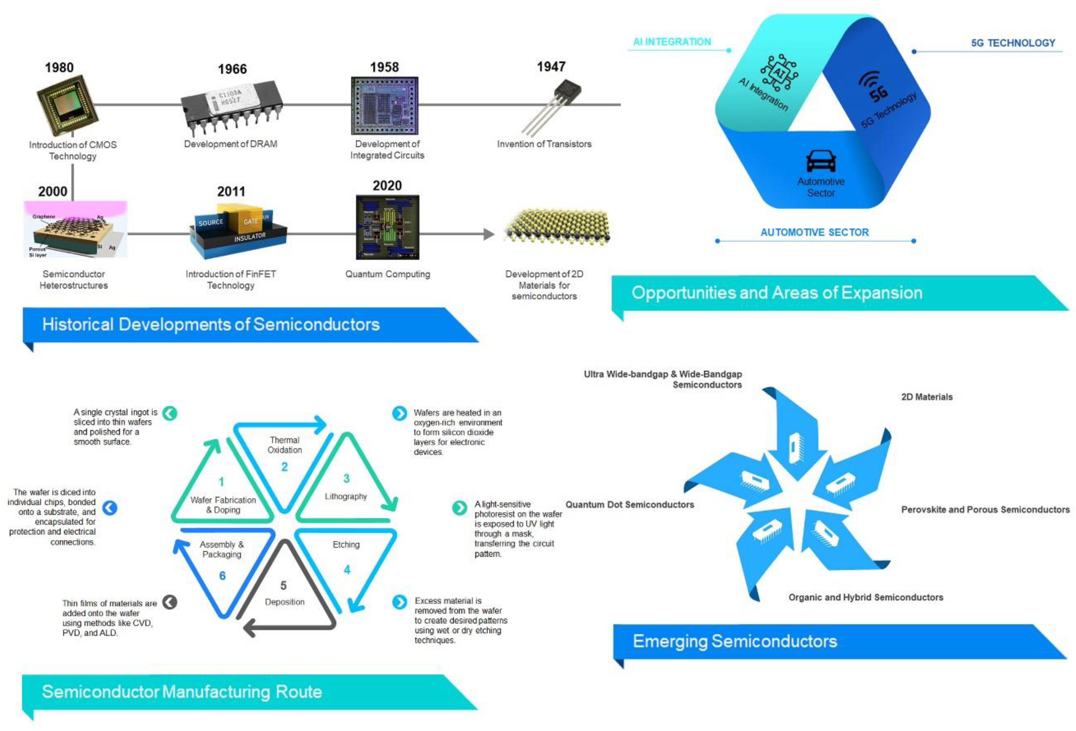
Figure 2.
Semiconductor Types; Classification of semiconductors into intrinsic (pure Ge, Si) and extrinsic (n-type with pentavalent impurities like P, As, Sb, and p-type with trivalent impurities like Ga, B, In, Al).[18].
Figure 2.
Semiconductor Types; Classification of semiconductors into intrinsic (pure Ge, Si) and extrinsic (n-type with pentavalent impurities like P, As, Sb, and p-type with trivalent impurities like Ga, B, In, Al).[18].
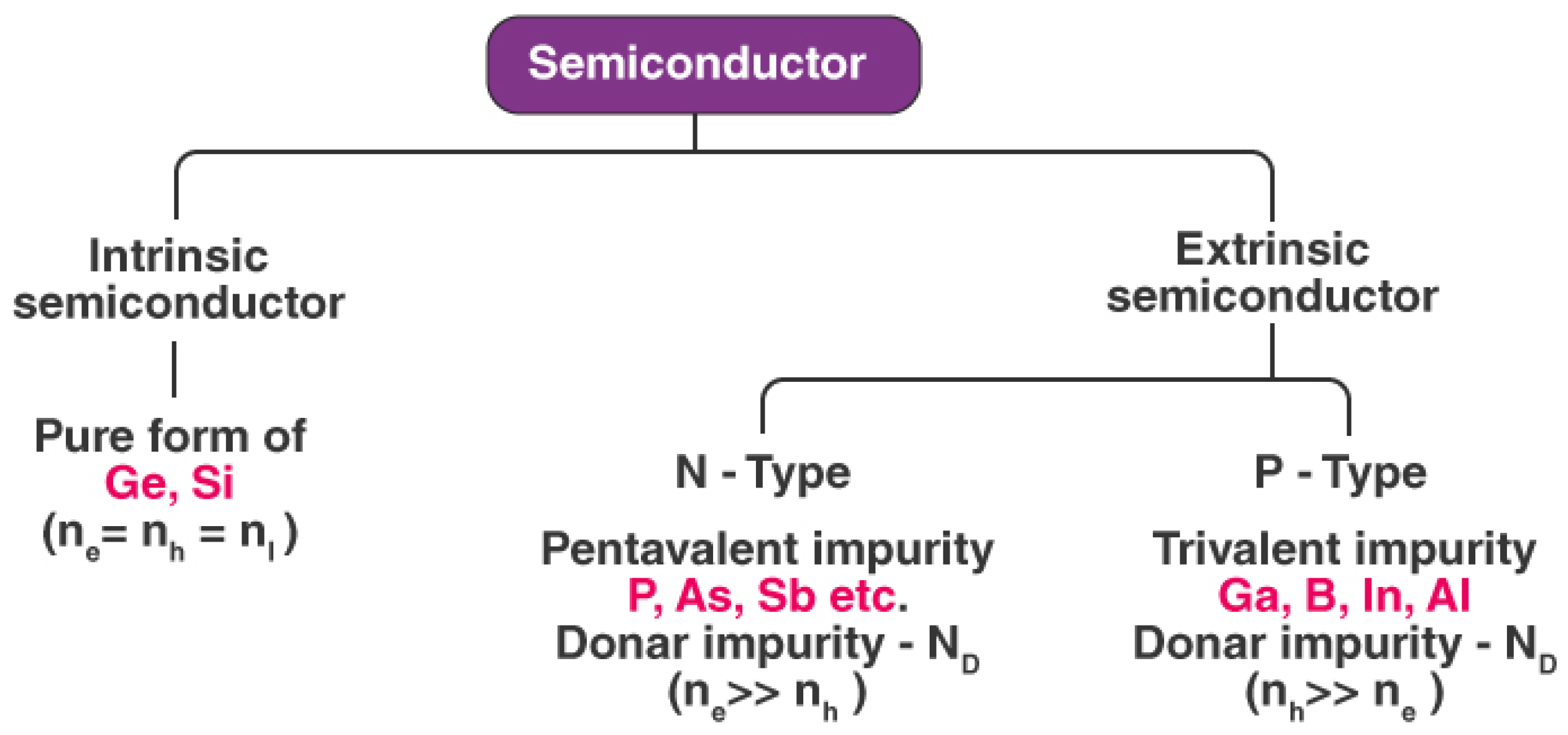
Figure 3.
Types of semiconductors; Semiconductor Doping and Charge Carrier Movement a) Intrinsic silicon with broken covalent bonds showing the creation of electron-hole pairs. The left panel depicts a free electron and its corresponding hole, while the right panel illustrates the movement directions of electrons (green arrows) and holes (yellow arrows) within the silicon lattice. b) Doped silicon showing n-type and p-type semiconductors. In the n-type semiconductor (left), a donor impurity (Pb) contributes free electrons to the silicon lattice. In the p-type semiconductor (right), an acceptor impurity (B) creates holes by accepting electrons, thus generating positive charge carriers [18].
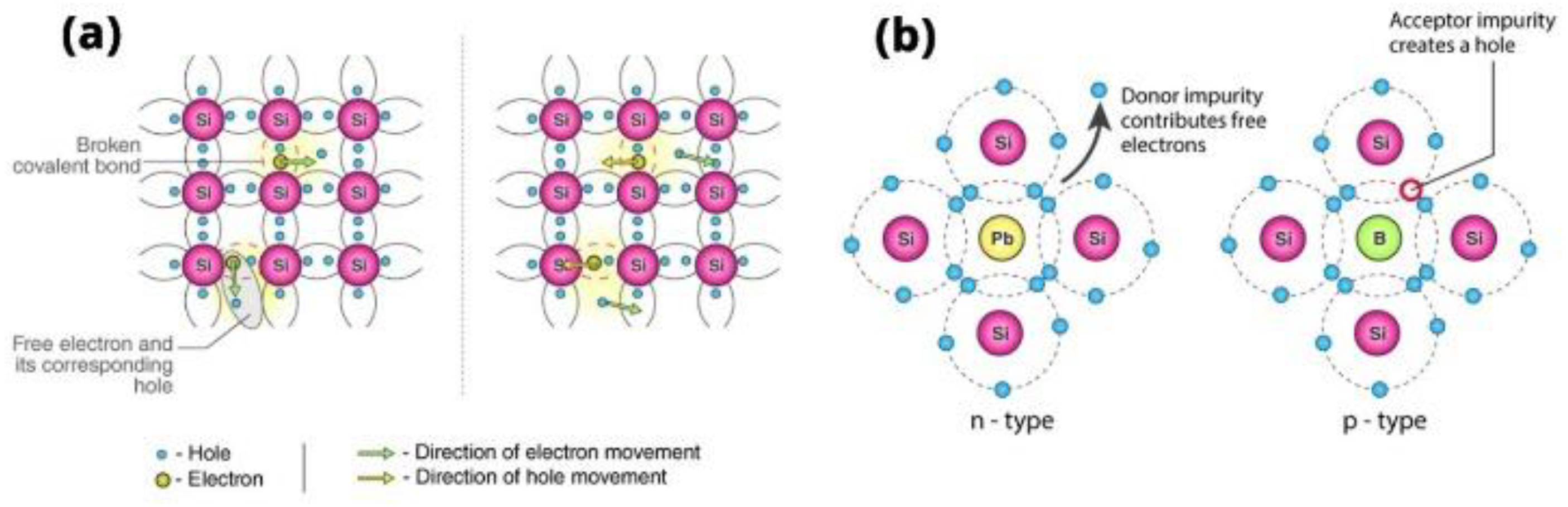
Figure 4.
Energy Band Diagrams. (a) Energy band structures of insulators, semiconductors, and conductors, showing the relative positions of conduction and valence bands. (b) Detailed view of the energy levels in semiconductors, illustrating electron energy transitions across the band gap (Eg). [18].
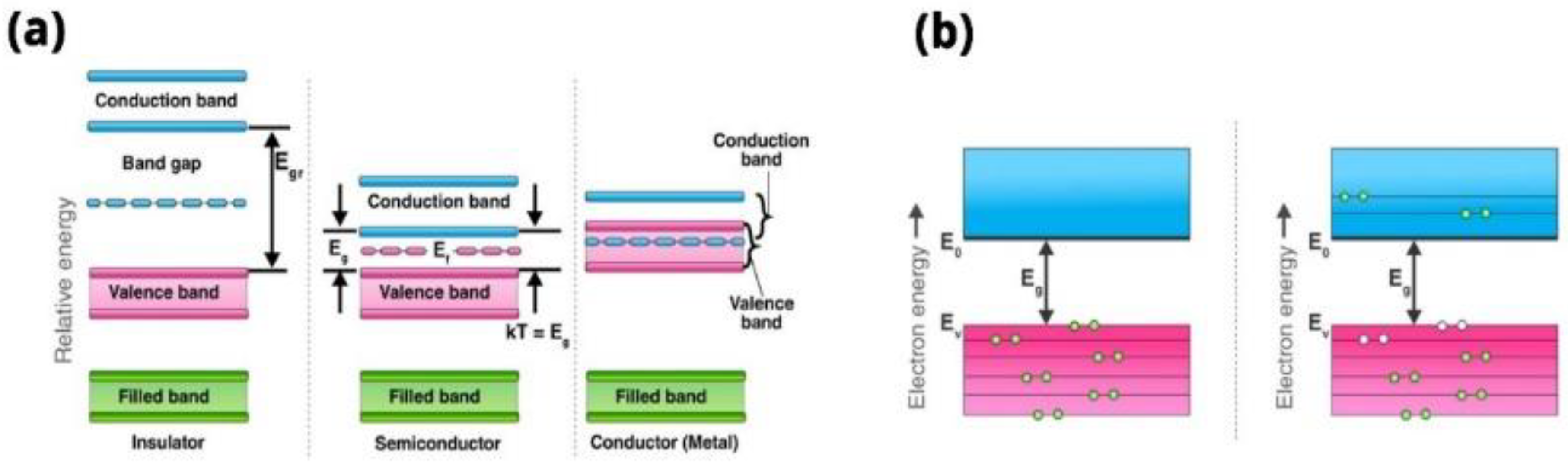
Figure 5.
(a) The evolution trend of the technology nodes for Si transistors [27]. (b) Flowchart of major historical semiconductor evolution.
Figure 5.
(a) The evolution trend of the technology nodes for Si transistors [27]. (b) Flowchart of major historical semiconductor evolution.

Figure 6.
The first-contact transistor [25] .
Figure 6.
The first-contact transistor [25] .
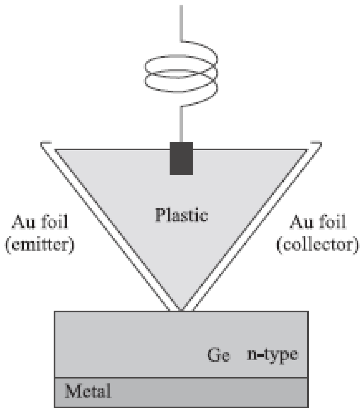
Figure 7.
Analysis of Tunnel Diode Characteristics and Working Principles. (a) Physical appearance of a tunnel diode. (b) Schematic diagram showing the structure of a tunnel diode, including the depletion region between the P-type and N-type materials. (c) Illustration of the tunneling effect in a PN junction, showing electron movement across the energy bands. (d) Detailed depiction of the tunneling effect in a tunnel diode, highlighting electron and hole movement through the narrow depletion region, enabling quantum tunneling. (e) Energy band diagram of an unbiased tunnel diode, indicating the alignment of the conduction band and valence band in P-type and N-type materials, and the absence of tunneling current. (f) Current-voltage (I-V) characteristics of a tunnel diode, demonstrating the peak current (Ip), valley current (Iv), and the region of negative resistance, highlighting the distinct tunneling current, negative resistance region, and conventional diode behavior. [50].
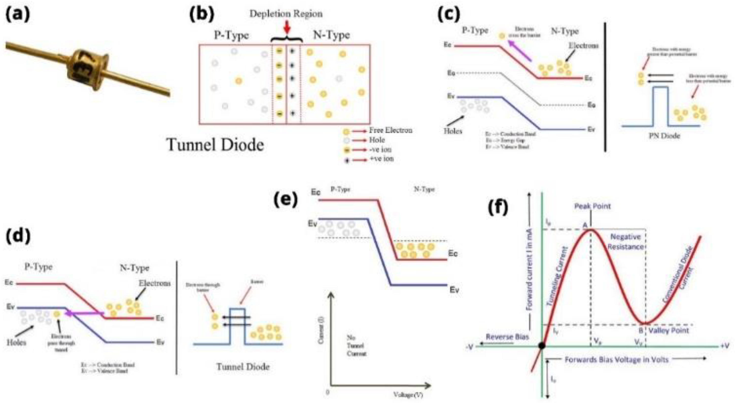
Figure 9.
(a) A cross-section of metal-oxide-semiconductor. (b) A cross-section of SOI MOSFET. Multigate transistor; (c) double gate (d) FinFET (e) Surrounding gate. [25].
Figure 9.
(a) A cross-section of metal-oxide-semiconductor. (b) A cross-section of SOI MOSFET. Multigate transistor; (c) double gate (d) FinFET (e) Surrounding gate. [25].
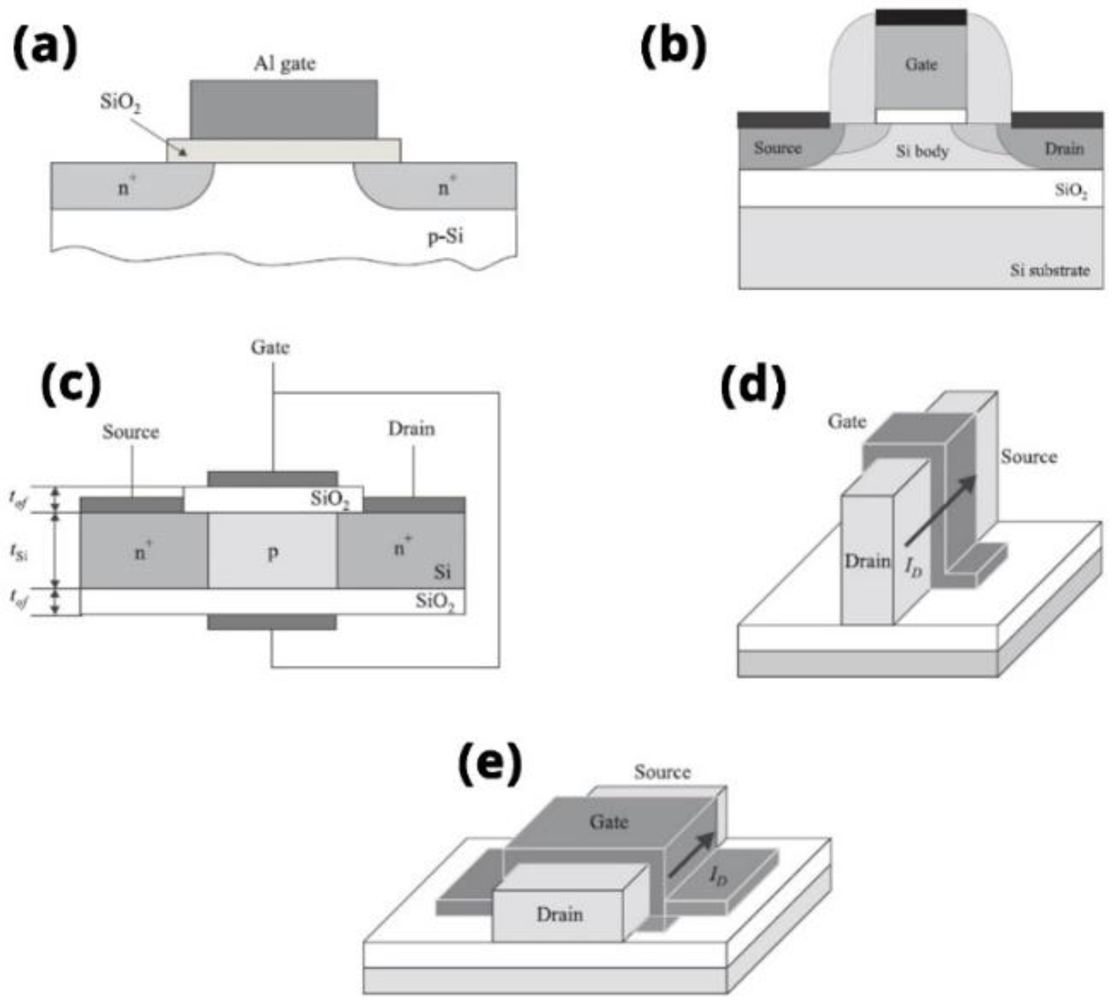
Figure 10.
Wide-bandgap Semiconductors analysis; (a) Comparing various semiconductor devices over power and frequency, highlighting the advantages of SiC and GaN over conventional silicon devices [118]. (b) Key differences between Si, SiC and GaN materials [119]. (c) Comparison of SiC and GaN devices in the market[120]. (d) Heat dissipation capabilities of GaN devices compared to SiC and Si, emphasizing the thermal advantages of GaN [121]. (e) Benchmarking vertical GaN devices against lateral GaN MOSFET devices and vertical SiC devices, illustrating the comparative performance metrics.[122]. (f) Fundamental efficiency limits of Si, SiC, and GaN technologies in bidirectional DC/DC converters, demonstrating the superior efficiency of SiC and GaN [123].
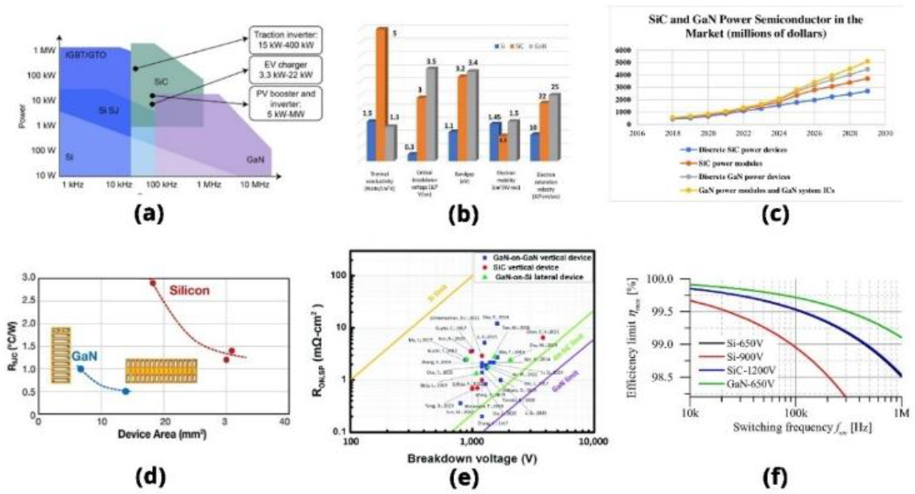
Figure 11.
(a) Bandgap energies of various semiconductors. (b) Characteristics and applications of UWBG semiconductor materials. [100].
Figure 11.
(a) Bandgap energies of various semiconductors. (b) Characteristics and applications of UWBG semiconductor materials. [100].
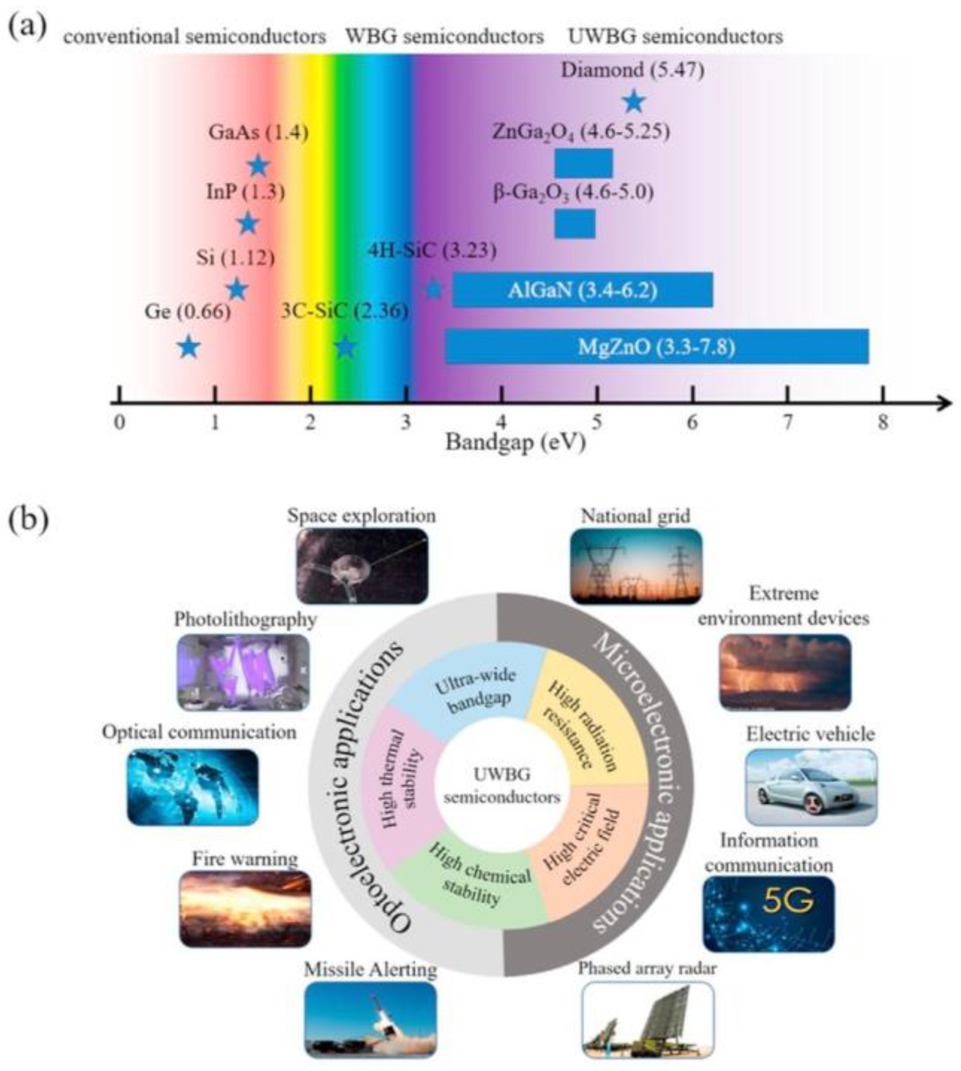

Table 1.
Common Semiconductor Material [1].
Table 1.
Common Semiconductor Material [1].
| The Portion of the Periodic Table Where Semiconductors Occur | ||||
| II | III | IV | V | VI |
| B | C | |||
| Al | Si | P | S | |
| Zn | Ga | Ge | As | Se |
| Cd | In | Sb | Te | |
| Elemental and Compound Semiconductors | ||||
| Elemental | IV Compounds | III-V Compounds | II-VI Compounds | Ternary Compounds |
| Si | SiC | AlP | ZnS | HgIn2Te |
| Ge | SiGe | AlAs | ZnSe | |
| AlSb | ZnTe | |||
| GaP | CdSe | |||
| GaSb | CdTe | |||
| InP | ||||
| InAs | ||||
| InSb | ||||
Disclaimer/Publisher’s Note: The statements, opinions and data contained in all publications are solely those of the individual author(s) and contributor(s) and not of MDPI and/or the editor(s). MDPI and/or the editor(s) disclaim responsibility for any injury to people or property resulting from any ideas, methods, instructions or products referred to in the content. |
© 2024 by the authors. Licensee MDPI, Basel, Switzerland. This article is an open access article distributed under the terms and conditions of the Creative Commons Attribution (CC BY) license (http://creativecommons.org/licenses/by/4.0/).
Copyright: This open access article is published under a Creative Commons CC BY 4.0 license, which permit the free download, distribution, and reuse, provided that the author and preprint are cited in any reuse.


