
Submitted:
04 September 2024
Posted:
05 September 2024
You are already at the latest version
Abstract
Energy generation now heavily relies on the field of photocatalysis. Many conventional research topics have been superseded by the conversion of solar energy into chemical or thermal energy for a variety of energy-related applications. The urgent necessity of moving away from non-renewable energy sources is a result of the problem of global warming. In an effort to create the best photocatalysts for effective solar conversion, scientists are investigating a variety of material systems and material combinations. By examining the influence of morphology changes on the photoelectrochemical activity of zinc oxide nanostructures, here electrodeposition was used to create the nanostructures. By using the proper capping agents, it is possible to control the growth rates of different ZnO facets and get well-defined nanostructures and orientation. In order to generate distinct ZnO morphologies, we report here the electrodeposition of ZnO nanostructured thin films in the presence of different capping agents. A zinc nitrate (Zn (NO₃)₂) bath was used to electrodeposit ZnO nanostructures on indium tin oxide glass (ITO) substrate at 70 °C with an applied potential of -1.0 V. Capping agents such as ethylenediamine (EDA) or ammonium fluoride (NH₄F) were added to this zinc nitrate bath. The photoelectrochemical capabilities of the morphology-controlled zinc oxide nanostructures were extensively evaluated and characterised. Thus various ZnO morphologies had an impact on the PEC properties.
Keywords:
Zinc oxide
; Electrodeposition
; Morphology
; Water splitting
; Nanostructure
; Photocatalysis
1. Introduction
The most significant cause of global warming, whose effects have started to appear in recent years, is carbon emissions from the combustion of fossil fuels [1,2,3]. As a result, it is critical to create clean, efficient, sustainable, and low-carbon energy sources in order to reduce global warming and reach carbon neutrality [4]. Since hydrogen emits no carbon dioxide when it is consumed, it is a viable clean energy source. In fact, hydrogen fuel cell technology is thought to be among the best ways to address the energy crisis in the future [5]. Fossil fuels and industrial waste products are the primary sources of industrial hydrogen production at the moment. Specifically, 80% of hydrogen production comes from coal and natural gas as raw materials, which also produces a significant quantity of carbon emissions throughout the production process [6]. The strategy of creating green hydrogen from solar water splitting has high hopes for realising hydrogen generation with zero carbon emissions. Furthermore, the storage issue of intermittent solar energy can be resolved by converting solar energy into chemical energy, such as hydrogen, methanol, or ammonia, among others. This enables a wider range of uses, including electric cars and peak shaving on the power grid [7].
Water splitting is an efficient process because it produces hydrogen from water, which is a plentiful and inexpensive material on Earth [8]. When exposed to high temperatures or radiation, water splitting can occur thermochemically, photobiologically, or photoelectrolytically. It can also occur photocatalytically, converting solar energy into chemical energy. A photocatalyst that has been activated by sun radiation breaks down water into oxygen and hydrogen in one or two steps during the photocatalysis process [9]. Using semiconductors as a photocatalyst is known as photocatalytic water splitting, and many semiconductors have been designed specifically for this purpose. A highly developed photocatalyst that can overcome obstacles in the water oxidation process is needed to achieve efficient photocatalytic water splitting. A positively topped valence band, a negative bottom to the conduction band, and a somewhat narrow band gap are required for the perfect photocatalyst. A small band gap, in the right place to produce an electron-hole pair for a redox reaction, improves solar energy harvesting. While the top of the valence band must be greater than the redox potential of water, the negative bottom of the conduction band promotes the quick release of hydrogen and the photooxidation reaction [10]. While semiconductor metal oxides and sulphides are widely employed as photocatalysts for water splitting, their employment accelerates the production of hydrogen [11]. As a result, advanced composites structures containing nanomaterials have been used. Because of their remarkable qualities, nanomaterials can also be directly utilised for photocatalytic water splitting or composited to improve these photocatalysts [8]. Controlling the structure and size of nanomaterials [12,13] can alter their bandwidth, and increasing the surface area to volume ratio leads to charge separation and inhibits hole-electron re-joining [14].
Several photocatalytically active materials, such as metal oxides, sulphides, nitrides, oxysulfide, carbon nitrides, and oxynitrides, have been examined for their ability to produce hydrogen from water [15,16,17,18,19,20,21]. Two of the materials that have been investigated the most are TiO2 and ZnO [22,23]. For free excitons, ZnO has a binding energy of 60 meV and a wide direct bandgap of 3.30–3.37 eV at 300 K [23,24]. Due to these two qualities, ZnO is an appealing choice for many optical and electrical applications [25]. Because ZnO has a higher electron mobility than TiO2 [26], this results in an increase in electronic transfer efficiency and a decrease in recombination process losses. ZnO has a band structure that is appropriate and satisfies the thermodynamic requirements for water splitting. As a photocatalyst, it is also inexpensive, non-toxic, and retains a high degree of crystallinity and stability. While ZnO’s conversion efficiency may not be as high as that of some metal sulphide semiconductor systems [27], its anisotropic growth and crystallisation capabilities make it a desirable alternative to other photocatalysts like ZnS, CuS, or other core-shell architectures [28].
The advantageous properties of ZnO nanostructures have thus been taken into consideration in the current study in order to fabricate a photocatalyst and examine the impact of morphological modification on its photoelectrochemical activities. Here, ZnO nanostructures have been fabricated via the electrodeposition method. Direct growth of these nanostructures was carried out on indium tin oxide glass (ITO) glass. Specific capping agents were employed as the morphology-modifying material throughout the electrodeposition process, resulting in the creation of ZnO nanostructures in a variety of densities and shapes. X-ray diffraction (XRD), scanning electron microscopy (SEM), UV-visible spectroscopy (UV-Vis), Photoluminescence and photoelectrochemical (PEC) measurements were used for analysing the synthesised nanostructures. In proof of concept studies, the current work examined the influence of morphology on the PEC performance of ZnO nanostructures.
2. Materials and Methods
2.1. Materials and Chemicals
Zinc nitrate hexahydrate (Zn(NO3)2·6H2O), which was bought from Fisher Scientific (Fair Lawn, NJ, USA), was the chemical used for ZnO deposition. Ethylenediamine (EDA) and ammonium fluoride (NH4F) were purchased from Sigma Aldrich (St. Louis, MO, USA). The substrate used for ZnO electrodeposition was indium tin oxide glass (ITO) on glass (size: 25 mm × 25 mm, resistivity: 7 ohm/cm2) purchased from University Wafer Inc. (Boston, MA, USA). Acetone, hydrochloric acid, and nitric acid were obtained from Fisher Scientific and implemented to clean and rinse the ITO substrate.
2.2. Electrodeposition of ZnO Nanostructures on ITO
ZnO was deposited onto the ITO on glass substrate using an electrochemical cell with three electrodes. The working electrode (WE) of the cell was the ITO on a glass substrate, the counter electrode (CE) was a platinum wire with a diameter of 2 mm, and the reference was Ag/AgCl wire electrode saturated in 1.0 M KCl.
ITO glass substrates were cleaned follows the same procedure as used in our previous work [29]. The ITO glass was cleaned in acetone using an ultrasonic cleaner for ten minutes prior to the electrodeposition of ZnO nanostructures. The substrate was then washed for two minutes in each of the hydrochloric and nitric acids in the following step. Between each cleaning procedure, distilled water was used to rinse the substrates.
The electrolyte solution for the electrodeposition of ZnO nanostructures was prepared by dissolving 50 mM of (Zn(NO3)2 in water. Using the CH1601E potentiostat, the ZnO nanostructure deposition was carried out for 30 minutes at 70 °C with an applied potential of -1.0 V. Ammonium fluoride (NH4F) and ethylenediamine (EDA) were the two capping agents used for the deposition of the modified ZnO nanostructures. Before electrodeposition, these capping agents were added to the electrolyte solution at a concentration of 15 mM and 10 mM respectively. The ZnO electrodeposition process parameters are given in Table 1.
2.3. Samples Characterisation
X-ray Diffraction (XRD) patterns were measured using a modified Bruker-Axs D8 diffractometer with parallel beam optics and a PSD LynxEye silicon strip detector. This instrument utilized an unmonochromated Cu Kα source operated at 40 kV with a 30 mA emission current. The incident beam angle was set at 0.5°, and the angular range of the collected patterns was 10° < 2θ < 65°, with a step size of 0.05° counted at 1 s/step. Scanning Electron Microscopy (SEM) was performed to determine surface morphology and film thickness using a JEOL JSM-6301F Field Emission SEM at an accelerating voltage of 5 keV. X-ray photoelectron spectroscopy (XPS) was conducted using a Themo K-Alpha spectrometer equipped with monochromated Al K-alpha radiation, a dual-beam charge compensation system, and a constant pass energy of 50 eV. Survey scans were acquired over the 0–1200 eV range, while high-resolution spectra were obtained for the principal peaks of Zn (2p), O (2p), C (1s), and Si (2p). Optical spectra were obtained using a PerkinElmer Fourier transform Lambda 950 spectrometer over a wavelength range of 300-2500 nm, encompassing the ultraviolet (UV), visible (Vis), and near-infrared (NIR) regions. The spectra were referenced against an air background. Photoluminescence (PL) spectra from 350 to 800 nm were recorded using an Edinburgh spectrofluorometer equipped with a maximum average power of 5 mW. The excitation wavelength used was 380 nm. The PL spectra were recorded under air at room temperature.
2.4. Photoelectrochemical Measurements (PEC)
Photoelectrochemical measurements of all photoelectrodes were conducted in a three electrode configuration in 1.0 M KOH electrolyte in Deionized water (DI), using an electrochemical workstation (A potentiostat (Metrohm)) under simulated sunlight (100 mW/cm2, AM 1.5 G). Ag/AgCl in saturated KCl was used as the reference electrode and Platinum wire used as a counter electrode. The illumination intensity was calibrated using a silicon reference cell with an optical meter (Newport, Model 1918-R). The electrochemical impedance spectroscopy (EIS) tests were conducted in the dark at open circuit potential across a frequency range from 105 and 10-2 Hz, with an AC voltage amplitude of 5 mV, using 12 points per decade. Mott-Schottky plots were tested over a potential range of −0.6 to 0.6 V (vs. Ag/AgCl) at a frequency of 1000 Hz.
3. Results and Discussion
3.1. Characterization of the Fabricated ZnO Nanostructures
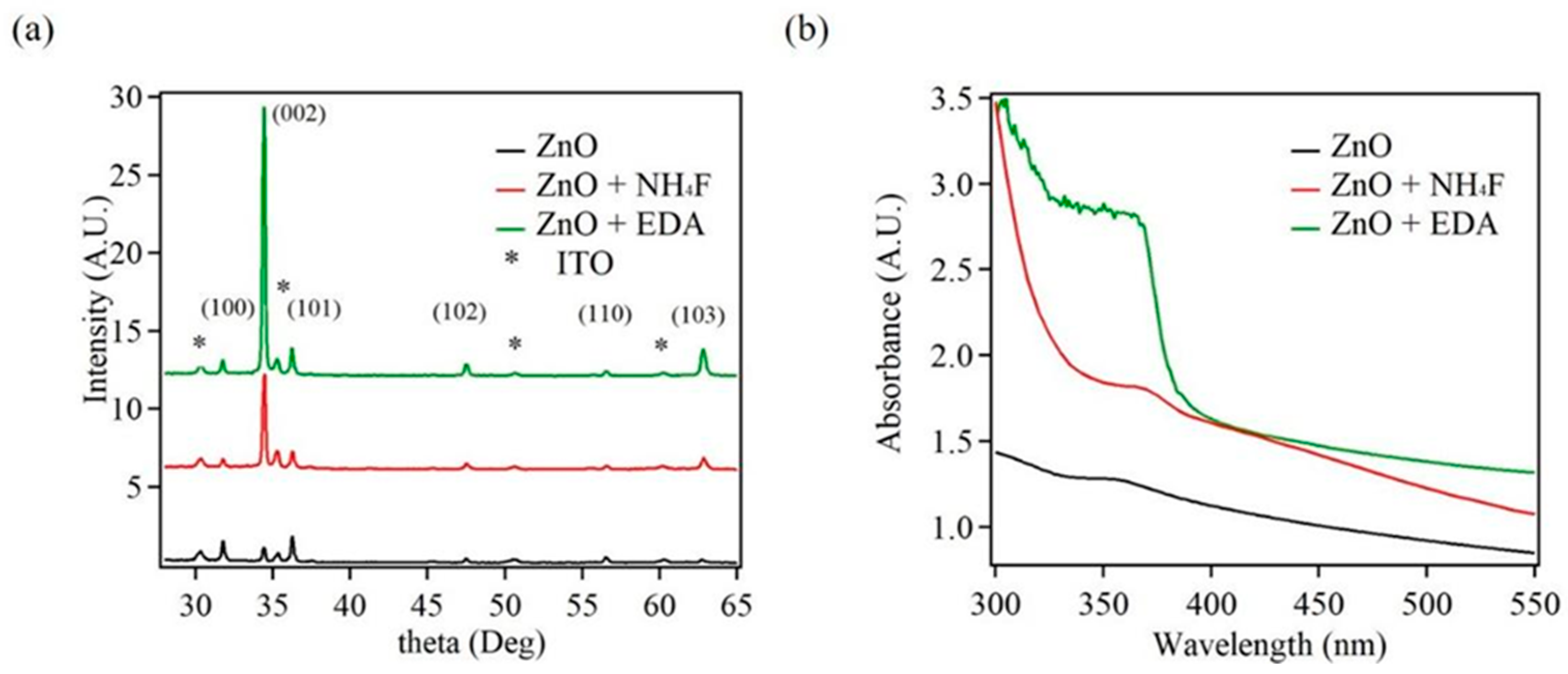
The crystalline nature and preferred orientation of the synthesised ZnO nanostructures were examined using XRD. There were three samples prepared for the investigation: unmodified ZnO, which was abbreviated as ZnO; ZnO nanostructures prepared in the presence of NH4F, which was abbreviated as ZnO + NH4F; and ZnO nanostructures prepared in the presence of EDA, which was abbreviated as ZnO + EDA. The ZnO nanostructures were subjected to XRD measurements in which XRD graphs of the three ZnO nanostructured samples are displayed in Figure 1a. For every sample, the XRD plot shows crystalline wurtzite structure. The plots and the JCPDS No. 36-1451 reference file were perfectly matched. The ZnO nanostructures showed a preferential orientation with a dominating (002) crystal plane at 2θ = 34.7° in the presence of capping chemicals. The XRD plots of ZnO + NH4F and ZnO + EDA showed this preferred orientation clearly and showed that the addition of the capping agents changed the morphology of the ZnO nanostructures.
In addition to XRD, UV-Vis measurement was performed on the ZnO nanostructures. Figure 1b shows an overview of these ZnO nanostructures’ absorption characteristics. ZnO nanostructures’ UV-Vis spectra revealed an absorption peak at 360 nm, corresponding to a bandgap of 3.45 eV. In contrast, samples ZnO + NH4F and ZnO + EDA showed a blue shift to 350 nm for the absorption peak, with a bandgap shift to 3. 35 and 3.0 eV respectively (Figure 3a). Thus changes in the morphology of ZnO nanostructures in the presence of the capping agents, NH4F and EDA, were identified as the cause of the blue shift in the absorption peak.
Figure 1.
(a) X-ray diffraction (XRD) plot and (b) UV-vis absorbance spectra of the ZnO, ZnO + NH4F and ZnO + EDA nanostructures.
Figure 1.
(a) X-ray diffraction (XRD) plot and (b) UV-vis absorbance spectra of the ZnO, ZnO + NH4F and ZnO + EDA nanostructures.
The morphological changes of ZnO in the presence of capping agents were confirmed by the characterizations indicated above. Moreover, SEM images of the ZnO nanostructures were acquired in order to observe these morphological modifications. The ZnO nanostructures’ images from a SEM are displayed in Figure 2. The ZnO sample Figure 2a showed structures that resembled hexagonal plates that were about 500 nm in diameter. The ZnO + EDA sample features a hexagonal rod nanostructure with a diameter of 1.2 μm and a thickness of 295 nm is seen in Figure 2b. The presence of EDA in the depositing electrolyte was the reason given for this change in morphology. As can be seen in Figure 2b, the morphological change was caused by the inclination to adsorb on a specific plane. In comparison to the ZnO reference sample in Figure 2a, the hexagonal particles in the ZnO + NH4F sample became thinner and smaller, generating a needle like nanostructure Figure 2c. The needles had a thickness of 50 to 300 nm and a maximum length of 10 μm. The morphology of the changed samples ZnO + EDA, and ZnO + NH4F differed significantly from the reference ZnO sample. The SEM images further show that the change in morphology during the synthesis of ZnO in the presence of chemical additives was successfully controlled.
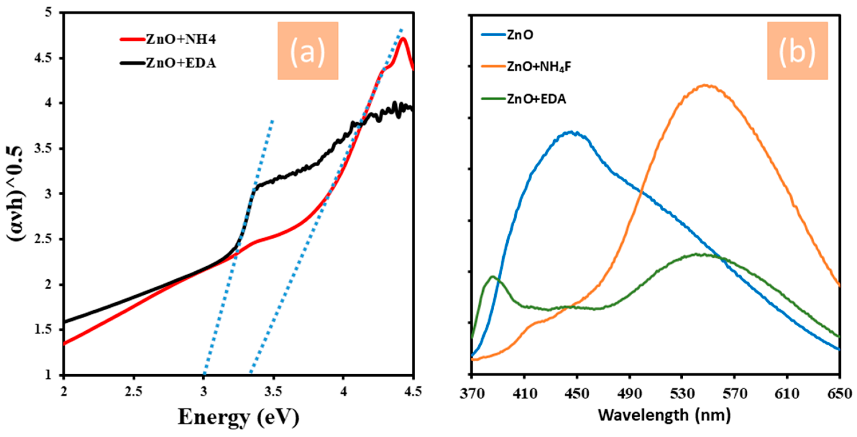
The emission of un-treated - ZnO nanoparticles and treated ZnO by NH4F and EDA in the UV−Vis and NIR regions were conducted using photoluminescence (PL), as depicted in Figure 3. Photoluminescence (PL) spectral emission is a valuable tool for studying charge carrier recombination and investigating the efficiency of charge carrier trapping, migration, separation, and transfer in semiconductors [30,31]. PL emission spectra arise from the radiative recombination of photoexcited carriers, with higher PL intensity indicating a greater extent of radiative recombination [32]. Figure 3. Shows the PL emission spectra of ZnO, ZnO + NH4F and ZnO + EDA nanostructure over a wavelength range of 370 to 650 nm, using an excitation wavelength of 380 nm. All samples showed distinctive peaks for PL. un-treated ZnO nanostructure shows a broad peak from 370 to 570 nm. Interestingly, the PL spectra of ZnO + NH4F are signifyingly different. It shows two peaks a broad and strong visible emission at 550 nm and a weak band emission at 390 nm. Meanwhile, the PL spectra of ZnO + EDA exhibits two weaker band and visible emissions, centred at 380 nm and 550 nm respectively. The emission band located at 380 to 390 nm is attributed to near-band emissions. The visible emission peak at 550 nm is attributed to various defects, including oxygen vacancies, zinc vacancies, and oxygen interstitials, which were formed by treating ZnO with NH4F and EDA, respectively [33].
Figure 3.
Band-gap and Photoluminescence (PL) of un-treated ZnO film, ZnO + NH4F and ZnO + EDA films prepared by electrodeposition method at 70 °C.
Figure 3.
Band-gap and Photoluminescence (PL) of un-treated ZnO film, ZnO + NH4F and ZnO + EDA films prepared by electrodeposition method at 70 °C.
The oxidation states of all samples on the surfaces were evaluated by X-ray photoelectron spectroscopy (XPS). The Zn 2p binding energy region in all samples showed Zn2+ character, with the 2p3/2 and 2p1/2 peaks centred at 1022.25 and 1045.31 eV, respectively, as shown in Figure 4. The ZnO treated by NH4F and ZnO + EDA exhibited no change in oxidation state, as they all showed the 2p3/2 and 2p1/2 peaks of at 1022.25 and 1045.31 eV, respectively, consistent with the untreated zinc sample, which represent Zn2+ character [34]. Figure 4d, shows XPS of spectra of O 1s core level for ZnO + NH4F, with the 1s peaks centred at 530.0 and 532.00 eV. According to the published reports, these peaks correspond to oxygen at lattice site and interstitial oxygen, respectively [35]. Notably, the XPS results did not reveal any impurities in the films, including fluorine or nitrogen.
3.2. Photoelectrochemical Measurements of ZnO Nanostructures
In this study, the influence of treating ZnO nanostructure films with NH4F and EDA during the preparation process and its effect on water splitting efficiency was investigated. To confirm the effect of the change in morphology on the photocatalytic activity of zinc oxide, which highlights their potential for utilizing sunlight as a renewable energy source. Photoelectrochemical water splitting (PEC) measurements were conducted in 1.0 M KOH (pH 13.5). Figure 5, shows linear sweep voltammetry (LSV) curves of un-treated ZnO, ZnO treated by NH4F and ZnO treated with EDA under two conditions: darkness and simulated sunlight (AM 1.5 G, 100 mW/cm2). As can be seen from Figure 5a, under dark conditions, the photocurrent of the untreated ZnO nanostructure sharply increases at a voltage of approximately 1.60 VRHE. However, under simulated sunlight conditions, the same sample exhibit a photocurrent peak of about 0.35 mA cm-2 at 1.23 VRHE, where RHE corresponds to the potential of the reversible hydrogen electrode. Also shown in Figure 5b is the photocurrent graphs of ZnO + NH4F, under sunlight conditions. We can see that treating by NH4F, caused an increase in photocurrent to reach 1.0 mA cm-2 at 1.23 VRHE. Meanwhile, ZnO treated with EDA reached a photocurrent of around 0.21 mA cm-2 at 1.23 VRHE as shown in Figure 5c. Which exhibited a lower photocurrent than untreated ZnO. For all samples, the current curves in dark conditions were increased by up to ~1.60 VRHE. Figure 5d, presents a comparison of photocurrent across all samples, revealing that ZnO + NH4F exhibited the highest photocurrent at 1.23 VRHE. It should be pointed out that the enhancement in PEC performance can be attributed to the influence of NH4F addition on the morphological changes in the ZnO + NH4F nanostructure. This is evident from the scanning electron microscopy (SEM) images (Figure 2), which reveal an increase in structural defects, such as the presence of oxygen vacancies. It has been reported in the literature that changes in the morphology of ZnO play a crucial role in enhancing photocurrent density and stability. It has been reported in the literature that changes in the morphology of ZnO play a crucial role in enhancing photocurrent density and stability. This enhancement is due to its effects on charge transfer from the electrolyte to the ZnO surface, as well as on carrier concentration and conductivity. Additionally, treating metal oxide surfaces with inorganic acids was found to increase the presence of hydroxide groups on the surfaces. These hydroxide groups enhance light absorption and introduce reactive sites on the metal oxide surface [36,37]. The solar-to-hydrogen (STH) conversion efficiency of the photoelectrode was determined using the following equation [38]:
where jph is the photocurrent density of the system, 1.23 V represents the theoretical minimum voltage needed for water splitting, and Pin is the incident light power, standardized at 100 mW/cm cm−2 under the AM 1.5 G spectrum with an intensity of 1 sun. Remarkably, the untreated ZnO photoelectrode achieved a maximum photocurrent of 0.35 mA/ cm−2 at 1.23 V vs. RHE, which corresponds to an STH efficiency of 0.40%. In comparison, the STH efficiency of a ZnO + NH4F photoelectrode thin film increased to 1.2%, a threefold improvement over the untreated ZnO thin films.
3.3. Electrochemical Impedance Spectroscopy (EIS)
Electrochemical impedance spectroscopy (EIS) is a powerful characterization technique utilized in various fields, including energy, electrocatalysis, and medicine. Two factors make the use of EIS particularly appealing. Firstly, EIS data can be employed to determine the physical characteristics of the electrochemical (EC) system under investigation, such as diffusion coefficients, chemical reaction rates, and microstructural properties. Secondly, setting up an EIS experiment is straightforward. Unlike standard EC techniques, which evaluate the relationship between current and applied potential difference in the time domain, EIS operates uniquely in the frequency domain. The EIS approach calculates the transfer function between current and potential. To measure EIS, an EC system is subjected to a small (preferably infinitesimal) sinusoidal voltage (in potentiostatic mode) or current (in galvanostatic mode) disturbance across a range of frequencies. The corresponding sinusoidal current or voltage response is simultaneously recorded. From this, a complex-valued function Z(f) is obtained, which depends on the perturbation frequency (f), through the voltage-to-current amplitude ratio and phase lag between input and output. It is important to note that EIS must satisfy the conditions of stability, linearity, and causality to be useful. Firstly, the EC system must be stable, as any variation over time will affect impedance frequency values. Secondly, the perturbation must be linear: if the applied sinusoidal disturbance has a sufficiently small amplitude, the response will be a sinusoid with the same frequency. However, if the amplitude of the sinusoidal input at a given frequency is large, the measured response will consist of superimposed sinusoids at frequencies f, 2f, and 3f. The third requirement is causality: the measured current (or voltage) must be a direct consequence of the applied voltage (or current) perturbation. Overall, EIS offers valuable insights into the physical and microstructural characteristics of EC systems, while its experimental setup is relatively straightforward compared to other EC techniques [39,40].
However, EIS measurements were employed to analyze the interfacial properties between the samples’ photoanode and electrolyte. The Nyquist plots, representing the imaginary and real components of the EIS plots (Z′ versus -Z″), were measured at 1.0 VRHE under dark and simulated sunlight conditions (AM 1.5 G, 100 mW/cm²) (Figure 6). The EIS was studied to determine the solution resistance and charge transfer resistance. As observed from Figure 6a, the un-treated ZnO + NH4F films shows the lowest values of Rct in the dark and simulated sunlight, while untreated ZnO + EDA films exhibit the highest values of Rct in both conditions (Figure 6c). Here, Rct represents the charge transfer resistance across the film-electrolyte interface. This is attributed to the excellent conductivity of the film. It is known that there is an inverse relationship between impedance and conductivity, and under light conditions, the conductivity of the ZnO + NH4F samples is stronger than that of the other samples in the 1.0 M KOH electrolyte, resulting in lower impedance. The NH4F addition to the samples during the deposition is believed to enhance the conductivity of the ZnO + NH4F films by reducing the recombination of hole-electron pairs, thus improving the photocurrent density. Overall, the ZnO + NH4F films demonstrate the best performance in terms of ionic and electronic transfer rates.
Mott-Schottky (M-S) calculations were used to investigate the flat-band potential (Vfb) and donor density (Nd) of untreated ZnO, ZnO + NH4F and ZnO + EDA nanostructure. Measurements were obtained at a frequency of 1.0 kHz, using the following equation [41,42,43]:
where A is the active area, e is the electron charge, εο is the permittivity of a vacuum, ε is the dielectric constant, T is the absolute temperature, kB is the Boltzmann constant, and E is the applied potential. The Mott-Schottky plots, shown in Figure 7, exhibited the n-type conductivity of all samples. From Figure 6a, it can be seen that untreated ZnO nanostructure reveals a flat band gap potential at -2.1 VAg/AgCl, and the flat band gaps of the treated ZnO with NH4F and EDA are calculated to be -5.0 and -2.5 VAg/AgCl , respectively as you can see in the Figure 7 (b and c). In comparison to the other samples, ZnO + NH4F displayed the highest negative flat band potential (Vfb) value. However, since the flat band potential (Vfb) of ZnO is typically around (-0.5 V vs. Ag/AgCl), our results for ZnO are generally consistent with those reported in the literature [44,45,46]. It was reported that a high negative flat band potential Vfb indicates a significant space charge region potential. This is crucial for photocatalytic activity in hydrogen reduction reactions, as the elevated flat band potential of the semiconductor provides a strong driving force to separate photo-generated electron-hole pairs in this region [30,47,48].
The stability of photoelectrodes is crucial for the generation and commercial viability of (PEC) hydrogen production devices. Consequently, methods to enhance the stability of semiconductors have garnered significant attention in recent studies. Figure 7 illustrates the stability of ZnO, ZnO + NH4F and ZnO + EDA nanostructure under simulated sunlight with an intensity of 100 mW/cm2. The ZnO + NH4F, remained stable for over 550 minutes (Figure 8b), maintaining a photocurrent density of approximately 1.5 mA/cm2. The ZnO + EDA nanostructure exhibited the lowest stability. As shown in Figure 8c, degradation of the film on ITO glass occurred immediately. In addition, untreated ZnO remain stable for less than 15 min (Figure 8a).
To verify that the photocurrent was directly generated from water splitting rather than from side reactions, the photogenerated hydrogen were measured using gas chromatography while applying a constant potential of 1.2 V vs. RHE. Hydrogen evolution from the samples anode were monitored at regular intervals. After 120 minutes of reaction, 79 and 120 μmol of hydrogen were detected for untreated ZnO and ZnO + NH4F anode respectively, as shown in Figure 9. This indicates that the hydrogen evolution of ZnO treated with NH4F is higher than that of untreated ZnO, it can be attributed to surface modification and improved charge transfer. This result suggests that, under an applied bias of 1.2 V vis. RHE, the photo-generated holes are able to migrate from the valence band of untreated and treated ZnO to the electrolyte.
Figure 10 illustrates the proposed mechanism for photoelectrochemical (PEC) water splitting using a ZnO photoanode under visible light illumination. The valence band (VB) position of ZnO is estimated to be 2.92 eV, while the conduction band (CB) position is around -0.33 eV, according to previous report [49]. The VB position of ZnO is more positive than the oxidation potential (1.23 eV vs. RHE), indicating that holes generated through photoexcitation in the valence band have sufficient potential to oxidize water. Concurrently, electrons are transferred from the conduction band of ZnO to the cathode, leading to water reduction. The morphological changes in ZnO enhance charge transport, thereby reducing the electron-hole recombination rate and improving the efficiency of hole-electron separation.
4. Conclusions
This paper shows the preparation of untreated ZnO nanostructure, ZnO treated by NH4F and ZnO treated by EDA on ITO glass substrate for spontaneous overall water splitting by using electrodeposition method. The addition of certain amount of NH4F during the deposition process showed significantly change in the morphology of ZnO nanostructure, as you can see from Figure 2. The ZnO treated with NH4F showed a significant increase in photocurrent compared to the untreated ZnO nanostructure in a 1.0 M KOH electrolyte, as noted in the PEC water splitting measurements. This improvement in the photocurrent was attributed to the impact of NH4F on the ZnO morphology. PL spectra investigations revealed that the enhancement in PEC performance was correlated with variations in the intensity of the PL spectra peaks.
These results are very promising and indicate exciting potential for developing advanced photocatalytic materials for green hydrogen production and clean energy. The successful application of NH4F treatment to enhance the PEC performance of ZnO nanostructure opens the door to further enhancement in water splitting efficiency and the advancement of sustainable energy technologies.
Author Contributions
Conceptualization, A.F. and S.P.; methodology, A.F., A.A. and S.P.; validation, software, M.K., L.A., A.B. and N.A. formal analysis, and data curation, A.F. and A.A.; writing—original draft preparation, A.F. and A.A.; writing—review and editing, A.F., A.A. and S.P.; supervision, project administration, funding acquisition, A.F., A.A. and S.P. All authors have read and agreed to the published version of the manuscript.
Funding
This research was funded by THE RESEARCH DEVELOPMENT AND INNOVATION AUTHORITY (RDIA), Kingdom of Saudi Arabia, grant number ”12866-KACST-2023-KACST-R-2-1-EI”.
Institutional Review Board Statement
Not applicable.
Informed Consent Statement
Not applicable.
Data Availability Statement
Data available upon request.
Acknowledgment
Thanks to the Center of Excellence for Advanced Materials and Manufacturing (KACST, Saudia Arabia). The authors would like to thank Mr. Ali Alanazi for useful discussion on PL results.
Conflicts of Interest
The authors declare no conflict of interest.
References
- Laufkötter, C.; Zscheischler, J.; Frölicher, T.L. High-impact marine heatwaves attributable to human-induced global warming. Science 2020, 369, 1621–1625. [Google Scholar] [CrossRef] [PubMed]
- Balch, J.K.; et al. Warming weakens the night-time barrier to global fire. Nature 2022, 602, 442–448. [Google Scholar] [CrossRef] [PubMed]
- Geng, T.; et al. Emergence of changing central-pacific and eastern-pacific El Niño-Southern Oscillation in a warming climate. Nature Communications 2022, 13, 6616. [Google Scholar] [CrossRef] [PubMed]
- Liu, Z.; et al. Challenges and opportunities for carbon neutrality in China. Nature Reviews Earth & Environment 2022, 3, 141–155. [Google Scholar] [CrossRef]
- Ma, T.; Lutkenhaus, J.L. Hydrogen power gets a boost. Science 2022, 378, 138–139. [Google Scholar] [CrossRef]
- Yang, X.; et al. Breaking the hard-to-abate bottleneck in China’s path to carbon neutrality with clean hydrogen. Nature Energy 2022, 7, 955–965. [Google Scholar] [CrossRef]
- Davis, S.J.; et al. Net-zero emissions energy systems. Science 2018, 360, eaas9793. [Google Scholar] [CrossRef]
- Kapoor, A.; Rajput, J.K. Nanostructured materials for the visible-light driven hydrogen evolution by water splitting: A review. International Journal of Hydrogen Energy 2022, 47, 17544–17582. [Google Scholar] [CrossRef]
- Villa, K.; et al. Photocatalytic water splitting: advantages and challenges. Sustainable Energy & Fuels 2021, 5, 4560–4569. [Google Scholar]
- Liu, Y.; et al. Bismuth-based complex oxides for photocatalytic applications in environmental remediation and water splitting: A review. Science of The Total Environment 2022, 804, 150215. [Google Scholar] [CrossRef]
- Ishaq, T.; et al. A perspective on possible amendments in semiconductors for enhanced photocatalytic hydrogen generation by water splitting. International Journal of Hydrogen Energy 2021, 46, 39036–39057. [Google Scholar] [CrossRef]
- Fallatah, A.; et al. Sensitive biosensor based on shape-controlled ZnO nanostructures grown on flexible porous substrate for pesticide detection. Sensors 2022, 22, 3522. [Google Scholar] [CrossRef] [PubMed]
- Fallatah, A.; et al. Influence of Morphology Change on Photoelectrochemical Activity of Cerium Oxide Nanostructures. Current Nanoscience 2023, 19, 285–290. [Google Scholar] [CrossRef]
- Chen, Y.-C.; et al. Photocatalytic enhancement of hydrogen production in water splitting under simulated solar light by band gap engineering and localized surface plasmon resonance of ZnxCd1-xS nanowires decorated by Au nanoparticles. Nano Energy 2020, 67, 104225. [Google Scholar] [CrossRef]
- Ameta, R.; Ameta, S.C. Photocatalysis: principles and applications. CRC Press, 2016. [Google Scholar]
- Tentu, R.D.; Basu, S. Photocatalytic water splitting for hydrogen production. Current Opinion in Electrochemistry 2017, 5, 56–62. [Google Scholar] [CrossRef]
- Ni, M.; et al. A review and recent developments in photocatalytic water-splitting using TiO2 for hydrogen production. Renewable and Sustainable Energy Reviews 2007, 11, 401–425. [Google Scholar] [CrossRef]
- Chen, W.-F.; Muckerman, J.T.; Fujita, E. Recent developments in transition metal carbides and nitrides as hydrogen evolution electrocatalysts. Chemical Communications 2013, 49, 8896–8909. [Google Scholar] [CrossRef]
- Merki, D.; et al. Amorphous molybdenum sulfide films as catalysts for electrochemical hydrogen production in water. Chemical Science 2011, 2, 1262–1267. [Google Scholar] [CrossRef]
- Akhundi, A.; et al. Graphitic carbon nitride-based photocatalysts: toward efficient organic transformation for value-added chemicals production. Molecular Catalysis 2020, 488, 110902. [Google Scholar] [CrossRef]
- Maeda, K.; et al. Efficient nonsacrificial water splitting through two-step photoexcitation by visible light using a modified oxynitride as a hydrogen evolution photocatalyst. Journal of the American Chemical Society 2010, 132, 5858–5868. [Google Scholar] [CrossRef]
- Chiarello, G.L.; Dozzi, M.V.; Selli, E. TiO2-based materials for photocatalytic hydrogen production. Journal of energy Chemistry 2017, 26, 250–258. [Google Scholar] [CrossRef]
- Samadi, M.; et al. Recent progress on doped ZnO nanostructures for visible-light photocatalysis. Thin Solid Films 2016, 605, 2–19. [Google Scholar] [CrossRef]
- Wang, Z.L. Novel nanostructures and nanodevices of ZnO, in Zinc oxide bulk, thin films and nanostructures. Elsevier, 2006; pp. 339–370. [Google Scholar] [CrossRef]
- Hou, T.-F.; et al. Vertically aligned one-dimensional ZnO/V2O5 core–shell hetero-nanostructure for photoelectrochemical water splitting. Journal of Energy Chemistry 2020, 49, 262–274. [Google Scholar] [CrossRef]
- Jayah, N.A.; et al. High electron mobility and low carrier concentration of hydrothermally grown ZnO thin films on seeded a-plane sapphire at low temperature. Nanoscale Research Letters 2015, 10, 1–10. [Google Scholar] [CrossRef]
- Zhang, K.; Guo, L. Metal sulphide semiconductors for photocatalytic hydrogen production. Catalysis Science & Technology 2013, 3, 1672–1690. [Google Scholar]
- Rokade, A.; et al. Electrochemical synthesis of 1D ZnO nanoarchitectures and their role in efficient photoelectrochemical splitting of water. Journal of Solid State Electrochemistry 2017, 21, 2639–2648. [Google Scholar] [CrossRef]
- Fallatah, A.; et al. Influence of Zinc Oxide Nanostructure Morphology on its Photocatalytic Properties. Current Nanoscience 2023, 19, 279–284. [Google Scholar] [CrossRef]
- Ghosh, S.; et al. Band-structure tunability via the modulation of excitons in semiconductor nanostructures: manifestation in photocatalytic fuel generation. Nanoscale 2023, 15, 10939–10974. [Google Scholar] [CrossRef]
- Cerrato, E.; Paganini, M.C.; Giamello, E. Photoactivity under visible light of defective ZnO investigated by EPR spectroscopy and photoluminescence. Journal of Photochemistry and Photobiology A: Chemistry 2020, 397, 112531. [Google Scholar] [CrossRef]
- Murali, A.; Sarswat, P.K.; Free, M.L. Minimizing electron-hole pair recombination through band-gap engineering in novel ZnO-CeO2-rGO ternary nanocomposite for photoelectrochemical and photocatalytic applications. Environmental Science and Pollution Research 2020, 27, 25042–25056. [Google Scholar] [CrossRef]
- Du, B.; et al. Defect passivation scheme toward high-performance halide perovskite solar cells. Polymers 2023, 15, 2010. [Google Scholar] [CrossRef] [PubMed]
- Sahai, A.; Goswami, N. Probing the dominance of interstitial oxygen defects in ZnO nanoparticles through structural and optical characterizations. Ceramics International 2014, 40, 14569–14578. [Google Scholar] [CrossRef]
- Pandey, S.K.; et al. Effect of growth temperature on structural, electrical and optical properties of dual ion beam sputtered ZnO thin films. Journal of Materials Science: Materials in Electronics 2013, 24, 2541–2547. [Google Scholar] [CrossRef]
- Weerathunga, H.; et al. Nanostructure shape-effects in ZnO heterogeneous photocatalysis. Journal of Colloid and Interface Science 2022, 606, 588–599. [Google Scholar] [CrossRef]
- Chen, Q.; et al. Synergetic effects of defects and acid sites of 2D-ZnO photocatalysts on the photocatalytic performance. Journal of Hazardous Materials 2020, 385, 121527. [Google Scholar] [CrossRef]
- De Silva, N.L.; et al. Superior solar-to-hydrogen energy conversion efficiency by visible light-driven hydrogen production via highly reduced Ti2+/Ti3+ states in a blue titanium dioxide photocatalyst. Catalysis Science & Technology 2018, 8, 4657–4664. [Google Scholar]
- Haritha, A.H.; et al. Sol–gel derived ZnO thin film as a transparent counter electrode for WO3 based electrochromic devices. Boletín de la Sociedad Española de Cerámica y Vidrio 2024, 63, 135–144. [Google Scholar] [CrossRef]
- Karmakar, S. Impedance Spectroscopy for Electroceramics and Electrochemical System. arXiv 2024, arXiv:2406.15467. [Google Scholar] [CrossRef]
- Sivula, K. Mott–Schottky analysis of photoelectrodes: sanity checks are needed. ACS Publications, 2021; pp. 2549–2551. [Google Scholar] [CrossRef]
- Ravishankar, S.; Bisquert, J.; Kirchartz, T. Interpretation of Mott–Schottky plots of photoanodes for water splitting. Chemical Science 2022, 13, 4828–4837. [Google Scholar] [CrossRef]
- Usler, A.L.; De Souza, R.A. A critical examination of the Mott–Schottky model of grain-boundary space-charge layers in oxide-ion conductors. Journal of The Electrochemical Society 2021, 168, 056504. [Google Scholar] [CrossRef]
- Adam, R.E. Synthesis and Characterization of Some Nanostructured Materials for Visible Light-driven Photo Processes. Linköping University Electronic Press, 2020; Vol. 2059. [Google Scholar]
- Liu, C.-F.; Lu, Y.-J.; Hu, C.-C. Effects of anions and pH on the stability of ZnO nanorods for photoelectrochemical water splitting. ACS Omega 2018, 3, 3429–3439. [Google Scholar] [CrossRef] [PubMed]
- Adam, R.E.; et al. Synthesis of ZnO nanoparticles by co-precipitation method for solar driven photodegradation of Congo red dye at different pH. Photonics and Nanostructures-Fundamentals and Applications 2018, 32, 11–18. [Google Scholar] [CrossRef]
- Yang, H. A short review on heterojunction photocatalysts: Carrier transfer behavior and photocatalytic mechanisms. Materials Research Bulletin 2021, 142, 111406. [Google Scholar] [CrossRef]
- Lei, W.; et al. Defect engineering of nanostructures: Insights into photoelectrochemical water splitting. Materials Today 2022, 52, 133–160. [Google Scholar] [CrossRef]
- Hussain, S.; Guo, L.; He, T. Influence of Vacancy Defects on the Interfacial Structural and Optoelectronic Properties of ZnO/ZnS Heterostructures for Photocatalysis. Catalysts 2023, 13, 1199. [Google Scholar] [CrossRef]
Figure 2.
SEM images of the surface of (a) ZnO, (b) ZnO + EDA and (c) ZnO + NH4F nanostructure grown by electrodeposition method on ITO glass.
Figure 2.
SEM images of the surface of (a) ZnO, (b) ZnO + EDA and (c) ZnO + NH4F nanostructure grown by electrodeposition method on ITO glass.
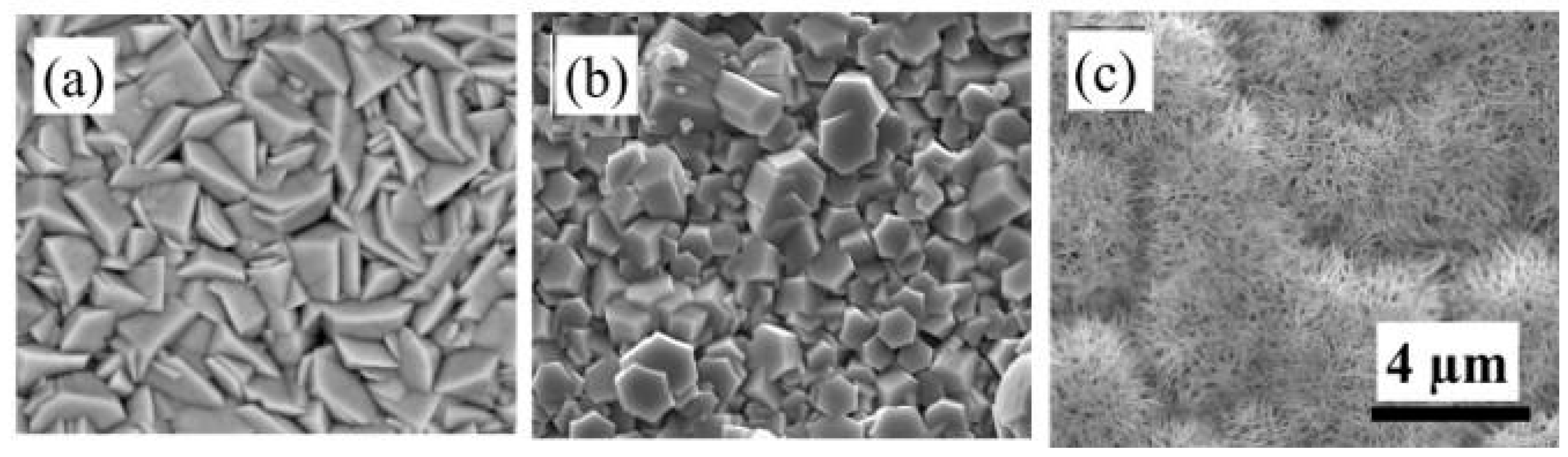
Figure 4.
Surface X-ray photoelectron spectroscopy (XPS) spectra of the Zn 2p1/2 and 2p3/2 core level scans in (a) un-treated ZnO film, (b) ZnO + NH4F, (c) ZnO + EDA films, (d) O 1s of untreated ZnO.
Figure 4.
Surface X-ray photoelectron spectroscopy (XPS) spectra of the Zn 2p1/2 and 2p3/2 core level scans in (a) un-treated ZnO film, (b) ZnO + NH4F, (c) ZnO + EDA films, (d) O 1s of untreated ZnO.
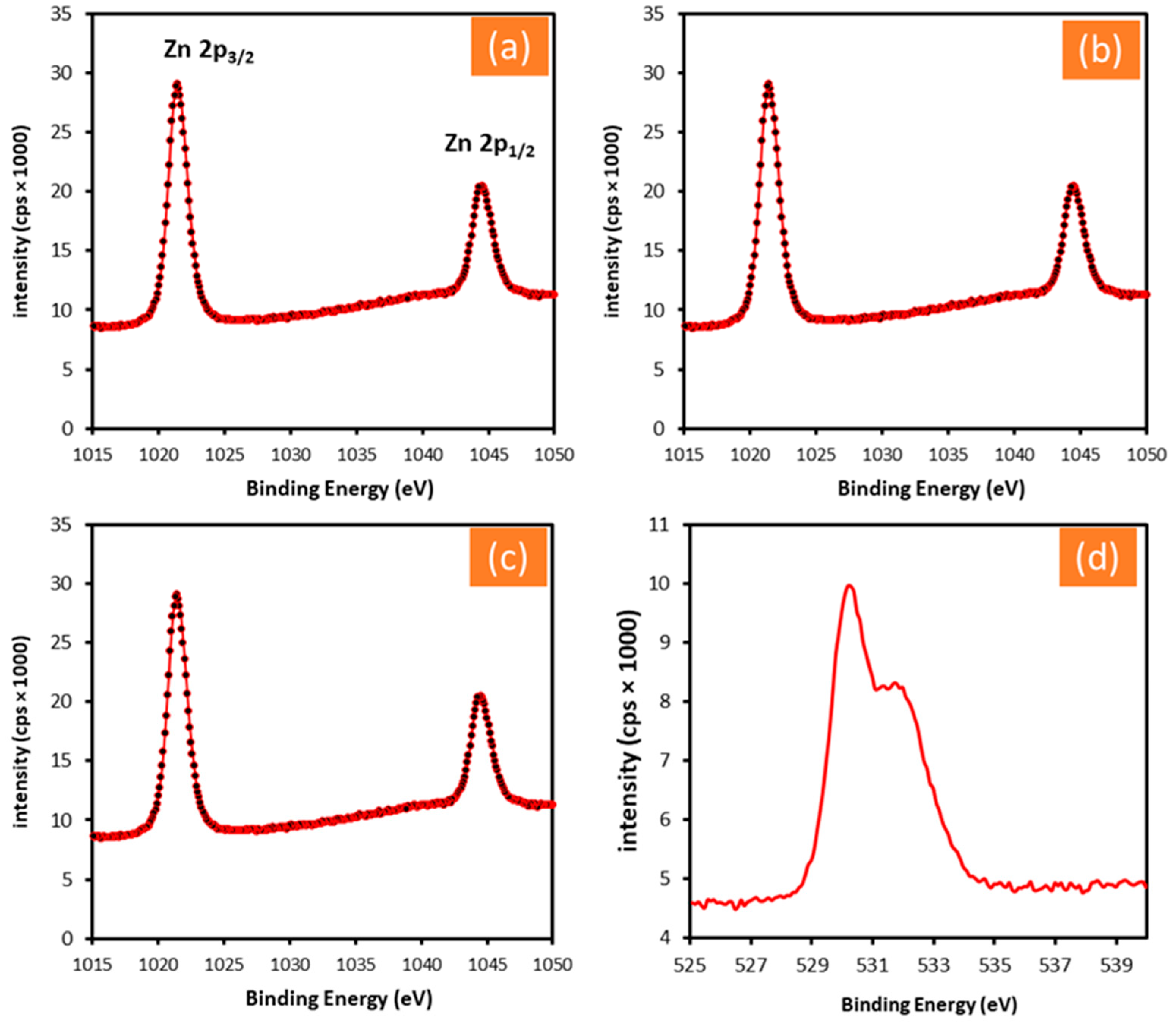
Figure 5.
Shows linear sweep voltammetry (LSV) curves of (a) untreated ZnO films, (b) ZnO + NH4F, (c) ZnO + EDA and (d) presents a comparison of LSV across all samples. all samples were measured under two conditions: darkness and simulated sunlight (AM 1.5 G, 100 mW/cm2) in 1.0 M KOH electrolyte and on ITO glass.
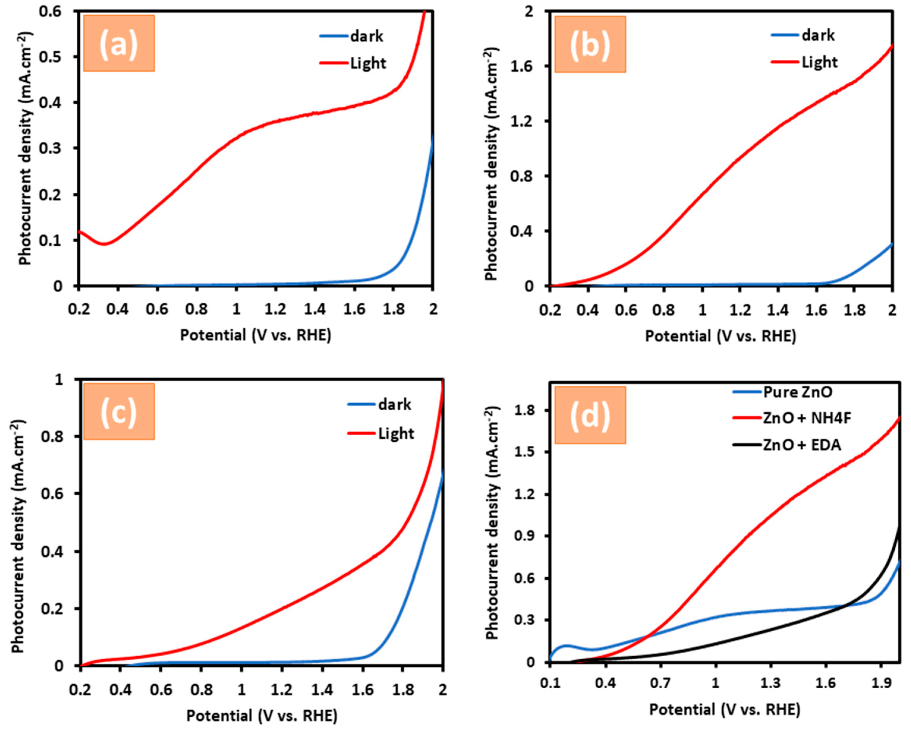
Figure 6.
shows electrochemical impedance spectroscopy (EIS) were measured under two conditions: darkness and simulated sunlight (AM 1.5 G, 100 mW/cm2) in 1.0 M KOH electrolyte and on ITO glass for (a) untreated ZnO, (b) ZnO + NH4F and ZnO + EDA films.
Figure 6.
shows electrochemical impedance spectroscopy (EIS) were measured under two conditions: darkness and simulated sunlight (AM 1.5 G, 100 mW/cm2) in 1.0 M KOH electrolyte and on ITO glass for (a) untreated ZnO, (b) ZnO + NH4F and ZnO + EDA films.
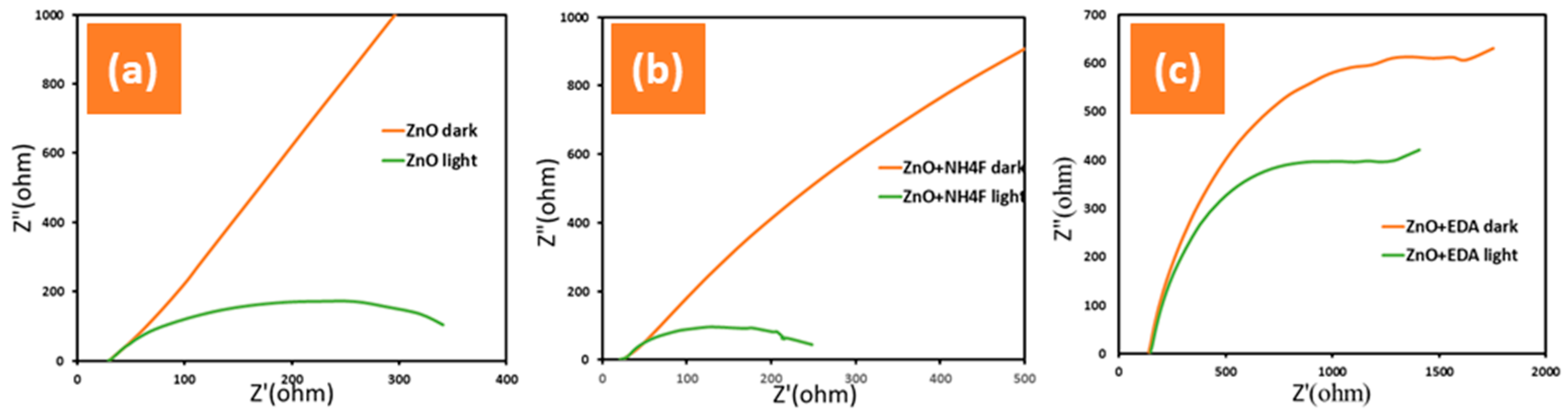
Figure 7.
Mott –Schottky plots for three photoelectrodes in 1.0 M KOH and under simulated solar illumination (100 mW/cm2), using (a) un-treated ZnO, (b) ZnO + NH4F and (c) ZnO + EDA nanostructure film. Flat band potential of the samples were calculated for this analysis.
Figure 7.
Mott –Schottky plots for three photoelectrodes in 1.0 M KOH and under simulated solar illumination (100 mW/cm2), using (a) un-treated ZnO, (b) ZnO + NH4F and (c) ZnO + EDA nanostructure film. Flat band potential of the samples were calculated for this analysis.
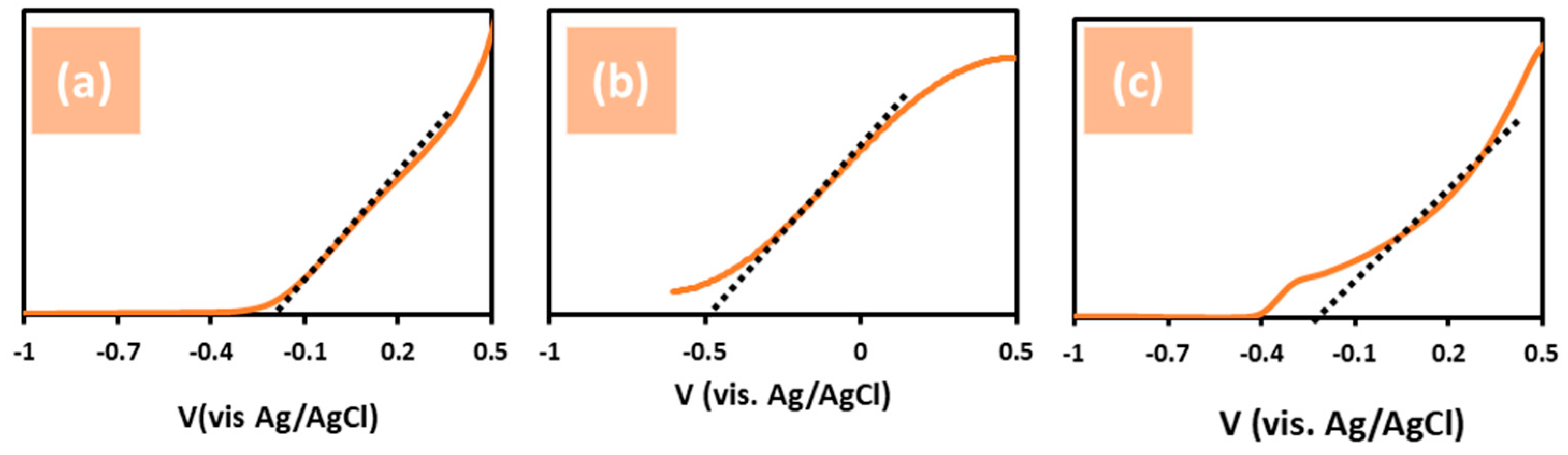
Figure 8.
The stability of (a) untreated ZnO, (b) ZnO + NH4F and (c) ZnO + EDA nanostructure films under simulated sunlight with an intensity of 100 mW/cm2 and photocurrent density of approximately 1.5 mA/cm2 in 1.0 M KOH electrolyte.
Figure 8.
The stability of (a) untreated ZnO, (b) ZnO + NH4F and (c) ZnO + EDA nanostructure films under simulated sunlight with an intensity of 100 mW/cm2 and photocurrent density of approximately 1.5 mA/cm2 in 1.0 M KOH electrolyte.
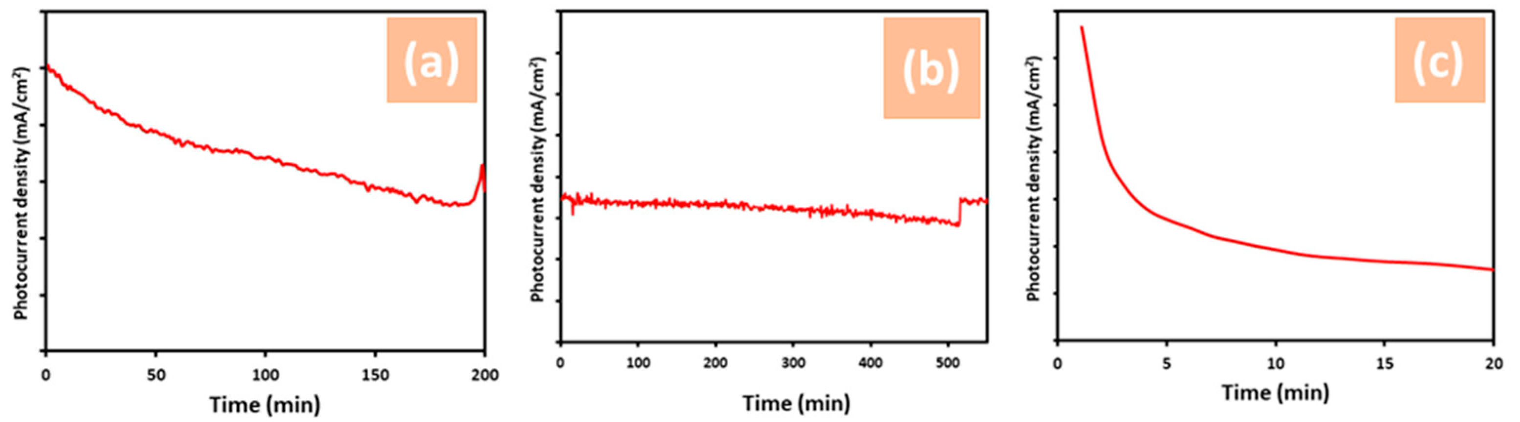
Figure 9.
Gas evolution of hydrogen and oxygen from the untreated ZnO and ZnO + NH4F anode as measured by gas chromatography (GC).
Figure 9.
Gas evolution of hydrogen and oxygen from the untreated ZnO and ZnO + NH4F anode as measured by gas chromatography (GC).
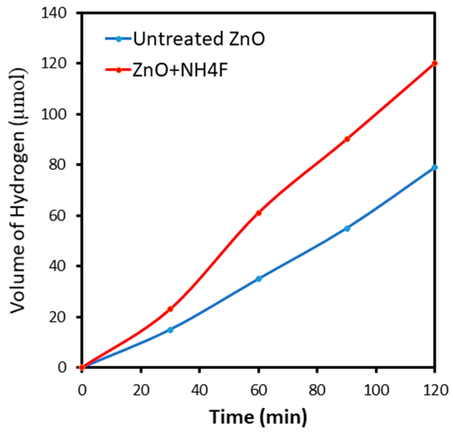
Figure 10.
Schematic diagrams depicting the photoelectrochemical (PEC) water splitting mechanism of ZnO nanostructure on an ITO substrate.
Figure 10.
Schematic diagrams depicting the photoelectrochemical (PEC) water splitting mechanism of ZnO nanostructure on an ITO substrate.
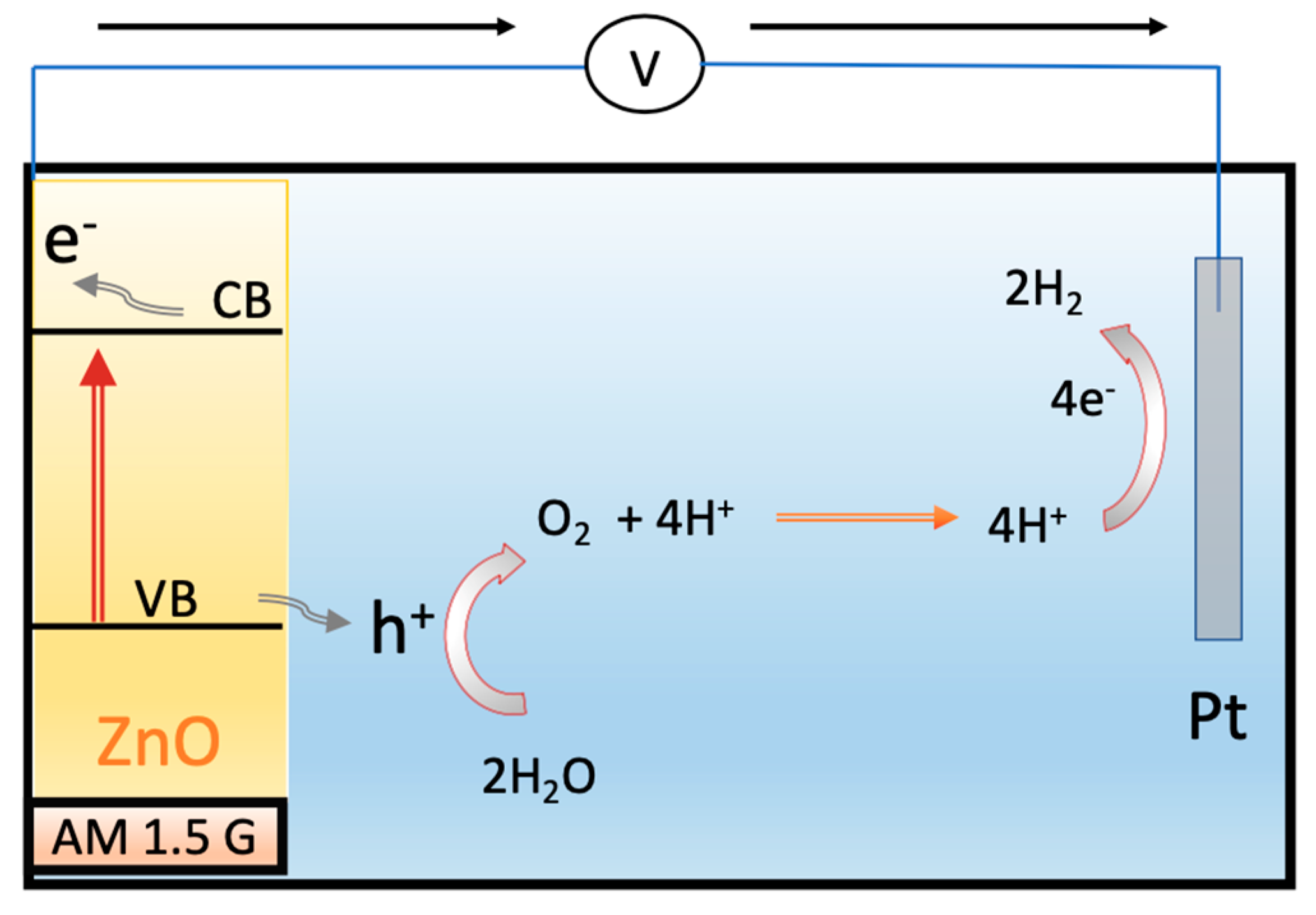

Table 1.
Process parameters used for the fabrication of the ZnO nanostructures.
| Process parameters | ZnO | ZnO + NH4F | ZnO + EDA |
|---|---|---|---|
| (Zn(NO3)2 (mM) | 50 | 50 | 50 |
| NH4F (mM) | 0.0 | 15 | 0.0 |
| EDA (mM) | 0.0 | 0.0 | 10 |
| Temp (°C) | 70 | 70 | 70 |
| Time (min) | 30 | 30 | 30 |
| Potential (V) | -1.0 | -1.0 | -1.0 |
Disclaimer/Publisher’s Note: The statements, opinions and data contained in all publications are solely those of the individual author(s) and contributor(s) and not of MDPI and/or the editor(s). MDPI and/or the editor(s) disclaim responsibility for any injury to people or property resulting from any ideas, methods, instructions or products referred to in the content. |
© 2024 by the authors. Licensee MDPI, Basel, Switzerland. This article is an open access article distributed under the terms and conditions of the Creative Commons Attribution (CC BY) license (http://creativecommons.org/licenses/by/4.0/).
Copyright: This open access article is published under a Creative Commons CC BY 4.0 license, which permit the free download, distribution, and reuse, provided that the author and preprint are cited in any reuse.


