Submitted:
30 August 2024
Posted:
03 September 2024
You are already at the latest version
Abstract
We extensively studied serigraphic screen-printed commercial silver flake inks loaded with silicon inclusions in order to achieve pinning at the grain boundaries. Based on grain size measurements using electron backscattered diffraction (EBSD), commercial silver ink with silicon microparticle content of 5 wt.% shows a significant grain growth retardation compared to the pristine silver ink, which stabilizes electrical conductivity up to 700 ◦C via Zener pinning mechanism. The modified silicon-loaded silver ink experiences a two times increase in grain size when heated up to 700 ◦C, compared to a seven times increase for the pristine silver ink. In turn, this enables operation temperatures significantly higher than the conventional operational window of microparticle-based silver inks, which are usually limited to 400 ◦C. Using isothermal exposures of 10 minutes up to 4 hours this phenomenon is observed at temperatures ranging from 250 ◦C to 900 ◦C. The electrical conductivity stability, grain size evolution and oxide contents were studied up to 4 hours. The activation energy of silver ink with silicon inclusions is 54% lower than for the pristine silver ink due to pining effect, which retards grain growth via the Zener mechanism. Most importantly, the electrical resistivity becomes stable up to 700 ◦C, which is more than twice the operation limit for off-the-shelf screen-printable silver flake inks. Hence, we demonstrate that adding controlled amounts of silicon particles to silver inks towards grain structure engineering can open new vistas of possibilities for screen-printed metallic inks.
Keywords:
Printed electronics
; Screen Printing
; high temperature inks
; silver flake inks
; grain boundary pinning
; Zener effect
; electron backscattered diffraction (EBSD)
; X-ray photoelectron spectroscopy (XPS)
1. Introduction
In recent years, the field of all-printed flexible hybrid electronics (FHE’s) have rapidly advanced towards creating functional, flexible and low cost devices for a variety of applications. Generally, FHE devices are limited in operational temperature by the thermal limits of the conductor (melting point) or polymeric substrate (glass transition temperature). In the context of high temperature applications, FHE technologies have immense potential towards delivering robust high temperature sensors and power electronics [1]. Key industrial sectors such as aerospace, oil and gas and chemical processing pose the opportunity to greatly benefit from the development of lost cost strain, temperature and pressure sensors to monitor critical systems and processes [2]. Conventional conductive inks and substrates are unable perform at conditions of elevated temperature generally exceeding 300 to 350 [3]. A robust and stable high temperature FHE device can be achieved by optimizing its three main building blocks: conductive ink, substrate and the passivisation over coat material [4]. A successful high temperature conductive ink should be able to maintain its high electrical conductivity, undergo minimal oxidation and remain stable over extended periods of time during its service life. Traditionally, high cost and harder to process precious metal inks such as nickel, gold, platinum and palladium have been employed to make high temperature sensors and devices [5,6,7,8,9].
Hence, there is an urgent need for low-cost and readily available inks that cater to high temperature applications. To address this, significant effort has been invested into improving traditional conductive inks via two distinct strangers; additives and alloying [1,4,10,11,12,13,14,15]. Passivating additives such as graphene have been used to minimize the oxidaiton of copper based conductive inks [1]. Similarly, , , and alloys have also been successfully investigated towards high temperature printed device applications [4,10,11].
Silver inks remain the most widely used due to their high electrical conductivity, stability and low oxidation potential [16]. It is estimated that silver inks held a market share of over 21% in 2023 [17]. Relatively low-costs and moderate sintering conditions make silver the material of choice for devices fabricated on low-temperature flexible polymeric substrates such as PET, PEN, polycarbonate, and Kapton® [18,19]. A large variety of silver inks are commercially available depending on the intended printing method. Silver nanoparticle based inks are used for direct-write printing such as inkjet, aerosol jet and micro-dispensing techniques [20], while silver micropartile inks are used for contact printing processes such as screen printing [21].
The sintering process and mechanism of the silver particle based inks have been detailed in literature by several researchers [19,22,23,24,25,26,27]. The sintering process can be broken down into two stages, densification and graing growth. Optimal sintering temperature is when maximum densification is achieved while retaining minimum grain size. This balance is challenging to achieve since denisification leads to grain growth as both processes have the same driving force and mass transport mechanism. Additionally, grain growth is required to reduce interfacial energy which eliminates pores and increases densification. Nano sized partiles tend to sinter at lower temperatures as compared to micron sized particles [28]. Typically, silver nanoparticle inks achieve complete sinteirng at 300 (0.3 T) [29]. Although microparticle screen printable inks are designed for low temperature substrates they tend to achieve complete sintering at 400 (0.42 T) [30] . Here, T is the is the melting temperature of bulk silver, which is 961 [31]. Beyond 0.42 T, significant grain growth is expected, which in turn alters the electrical properties and stability of the devices [30]. Thus, the operational window generally acknowledged for screen-printed silver devices is up to 400 . Although this satisfies most applications, high temperature FHE applications demand operation in temperatures exceeding 500 [2].
Grain growth is a well-known physical mechanism where the average grain size of a poly crystalline material increases when external energy is applied [32]. Grain boundaries are complex structures at crystalline domain interfaces typically 1-2 unit cells in width with higher Gibbs free energy than the bulk crystalline material. When external energy is applied to the poly crystalline material, grain boundaries move due to diffusion of atoms from convex grains into concave grains resulting in the grain boundary moving to the center of the concave grain. This is termed as grain coarsening leading to the reduction in grain boundaries and hence reducing the free energy of the poly crystalline material [33,34].
Electrical conductivity is largely dependant on grain size due to presense of trapping sites at the grain boundaries which influence electron mobility [35]. Electrical conductivity () of nanoparticle-based inks is inversely proportional to the grain size [25,26] where as of microparticle-based silver inks is expected to increase with higher grain sizes up-to 850 [28,30]. However, mechanical properties such as hardness and Young’s modulus tend to reduce with increase in grain size [27,32,33,36]. Here, it is imperative to find a optimal grain size to achieve desired mechanical and electrical properties of the printed film depending on the application at hand.
Building on the pioneering work initiated by Zener-Smith, it was shown that the inclusion of controlled amounts of secondary phase particles helps in achieving grain growth control [37]. This phenomenon is called grain boundary pinning or Zener pinning, where dispersion of secondary phase particles creates a pinning pressure that obstructs grain boundary movement to limit grain growth. Very limited work has been done to exploit such grain boundary control strategies using inclusions to engineer printable materials. Copper nanoparticles were previously alloyed with with gold [38], graphene [39] and silicon carbide [34] to achieve grain growth retardation, allowing for superior mechanical properties of the alloy for flexible printed device applications. Yttrium stabilized zirconia was also added to silver ink, retarding grain growth up-to 740 [40].
This study focuses on the process of grain growth and grain pinning of already sintered samples prepared as if they were to be used under ambient applications. Limited work is found on the electrical stability of printed silver inks at higher temperatures. It is reported that a significant increase in the grain size occurs for aerosol jet-printed silver ink at 500 , along with improved oxidation resistance and electrical stability at elevated temperatures [41]. Stability over long exposure time duration’s is a critical parameter for the longevity and performance of high temperature devices. This works seeks to provide a thorough understanding of the impact of refractory inclusions and how they can be used to control and improve the properties of commercial silver inks for operation at higher temperatures. Intrinsic silicon particles are used due to their low electronic band-gap at room temperature of 1.12 eV and high electron mobility of 1350 cm2 (V.s)-1 [42]. This allows for a smaller reduction in electrical conductivity of the modified ink as compared to more stable metal-oxide and carbides-based ceramics [42].
2. Materials and Methods
2.1. Materials
Widely-used commercial screen-printable silver flake-based ink Metalon® HPS-FG32 was purchased from Novacentrix Inc. Austin, TX, USA. The ink is 75 wt.% loaded with 1.5 m silver flakes dispersed in a, w Butyl Carbitol-based solvent system. Silicon powder > 99% with particles 1-5 µm in diameter was purchased from US Research Nanomaterials Inc., Huston, TX, USA (Product: US1127). In order to study the evolution of grain size at high temperatures, Alumina substrates were employed due to their excellent high temperature stability. 0.2 inch thick Aluimina sheets were purchased from Mcmaster Carr Elmhurst, IL, USA (Product: 8462K26) and cut into 1 inch square coupons using a wet time cutting saw. No modifications were made to any of the materials upon receipt.
2.2. Ink Formulation
Modified () ink was formulated by incorporating 3, 5, 7 and 10 wt.% loading of microparticles in the pristine ink. To achieve homogeneous dispersion, a two step process is employed. The microparticles were weighed and added in approximately two portions. Each portion was added to the pristine ink followed by through mixing using a Thinky ARE-310, Laguna Hills, CA, USA planetary mixer for three cycles of one minute at 2,000 rpm followed by one minute of rest intervals to allow ink degassing. This mixing procedure ensured a stable dispersion of the ink formulations with a shelf life of over six months.
2.3. Sample Fabrication
Cut alumina substrates were prepared by cleaning with 9.99% pure acetone (Millipore Sigma 270725). A simple 17 mm × 12 mm rectangular feature is fabricated into a 325-mesh stainless steel mesh screen as depicted in Figure 1(a); providing a 25.4 µm wet film thickness after manual screen-printing (one pass)as seen in Figure 1a). Three samples per test temperature were fabricated for each of the modified () formulations to ensure repeatibility and reliability of the collected data. As recommended by the silver ink manufacturer, the samples are sintered in a Mancorp, Montgomery County, PA, USA (MC301N) reflow oven at 250 for 60 minutes in air to remove all organic components of the ink and initiate densification.
2.4. Testing and Characterization
We studied the evolution of grain structure and electrical conductivity of the pristine and () inks with incremental temperatures and exposure times. The samples were exposed to temperatures in incremental steps of 100 with a ramp of 10 min between 400 and 900 for 10 mins, 1,2,3,4 hour of isothermal exposure times. The samples were then allowed to cool down naturally to room temperature. The thermal treatment was limited to 900 ) to stay below the melting point of silver ( 961 ) [43]. The entire thermal process is depicted in the Figure 1b).
Raman micro-spectra of the modified () inks was obtained using the WITec alpha300A (Ulm, Germany) raman microspectoscopy system with a 532 green laser. Particle size distribution of particles was determined using a Zetasizer Lab system (Malvern Panalytical Ltd, Malvern, UK). Micrographs of the printed films were obtained using a Hitachi SU8230 (Tokyo, Japan) scanning electron microscope (SEM) equipped with a Bruker (Billerica, MA, USA), QUANTAX FlatQUAD EDX detector for precise elemental mapping. The SEM is also equipped with a Bruker e-Flash HR+ detector to acquire Electron back-scattering diffraction (EBSD) micrograhs. Ossila T2001A3 (Sheffield, UK) four-point-probe was utilized to measure the electrical conductivity of the printed silver films. X-ray photoelectron spectroscopy (XPS) was performed using Thermo Fisher, VG ES- 245 CALAB 250Xi equipped with a cobalt source. Thermal galvanometric analysis TGA was performed using a Perkin Elmer’s STA8000 system Waltham, MA, USA.
3. Results and Discussion
3.1. Material Characterization
The Raman spectra of the modified () is presented in Figure 2a). The band at 233 cm-1 is attributed to the stretching mode [44]. The vibrational peaks at 517 cm-1 and 666 cm-1 are due to the stretching vibrations of and , respectively [45]. The bands at 1353 cm-1, 1594 cm-1 are associated with the symmetric and anti-symmetric stretching vibrations of the carboxylic group [46]. The peaks at 980 cm-1 and 517 cm-1 are from the silicon particles which is slight shifted as compared to crystalline silicon with a peak at 520 cm-1 [47,48]. We further analysed the particle size distribution of the as received particles. Figure 2b) suggests a size range between 800 nm to with an average particle size of . Thermal galvanometric analysis (TGA) (Figure 2c)) of both inks shows a significant drop in wt.% starting at around 120 until 250 , suggesting complete solvent burn off consistent with the boiling point Butyl Carbitol at 231 . A further drop in wt.% between 250 and 366 can be speculated to originate from the removal of other organics in the ink matrix such as proprietary surfactants and dispersants used by the ink manufacturer (Figure 2c)). It is worth noting that the weight fraction of the modified () ink is slightly higher than the silver ink, most likely due to the mass contribution of the silicon particles in the modified ink. The weight % of both inks remains stable beyond 400 , suggesting a complete sintering of the silver flakes beyond this point [49]. After initial sintering of the pristine ink, at 250 (for 1 hour), the silver flakes show signs of necking while maintaining their shape and structural integrity indicating onset of densification (Figure 3a)). As seen in the EDX micrograph of the modified () ink (Figure 3b)), silicon particles (highlighted with red arrows) are uniformly dispersed across the printed and sintered film.
3.2. Evolution of Electrical Conductivity
Over the entire temperature range we observed the impact of grain growth and grain pinning on the electrical conductivity of both inks which was studied. To study this effect, electrical conductivity was measured via four point probe for three samples processed at each incremental treatment temperature. Each samples was probed 3 times with a samples set of 100 data points per test. In total, 900 data points of electrical conductivity were collected per samples point. The evolution of electrical conductivity of the pristine ink (1 hour isothermal time per treatment temperature) is presented in Figure 4a). Conductivity data for all test cases has been summarized in Table S2 in the supplemental section. After initial sintering at the manufacturers recommended conditions, the pristine ink achieves an electrical conductivity of 4.14 (± 0.27) x S/m which is appromitaley one third compared to the conductive of bulk silver of 6.2 x S/m [50]. The conductivity further increases up to 500 with a maximum value of 5.6 (± 0.28) x S/m as grain growth continues leading to the reduction of the mean free path and micro pores leading to densely packed film. Beyond 500 , we observe a fall in electrical conductivity owing to the formation of pores due to continued densification of the films micro structure.
Figure 4b)-e) show the evolution of electrical conductivity of the modified () inks with 3, 5, 7, 10 wt.% loading of particles treated at incremental temperatures for 1 hour isothermal exposure. Here we note that the conductivity of all the modified () inks at 250 is lower compared to the pristine . This reduction can be attributed to the presence of insulating particles in the inks. Amongst these, the 3 and 7 wt.% loaded inks show a initial increase in conductivity up to 400 indicating complete sintering followed by a reduction in conductivity due to increased grain growth. Beyond 700 these inks follow behave erratically.
The 10 wt.% loaded ink follows a different behavior, where the conductivity reduces up to 500 and then tends to increase gradually until 700 followed by a sudden drop in conductivity. The 5 wt.% loaded ink by far was the most stable formulation. After complete densification is achieved at 400 , the electrical conductivity remains extremely stable up to 900 . This formulation has the potential to provide the optimal balance between densification and grain growth allowing stable electrical performance at ultra high temperatures while maintaining a relatively low average grain size in the printed film micro structure allowing for optimal mechanical properties towards the desired applications. Here on, we further examine the properties of the modified () ink as compared to the pristine ink.
A robust and stable device needs to maintain its properties over long duration of time especially in extreme environments where factors such as oxidation can play a detrimental role. To examine the electrical stability of the modified () ink, we tested freshly prepared samples at each temperature up to 4 hours of isothermal exposure. Figure 4f)-k) compare the electrical conductivity of the pristine and 5 wt.% modified ink. Error bars are omitted for the simplicity of graphical representation, however conductivity data with standard deviations are presented in Table in the supplemental section.
For the modified () ink up to 400 , the electrical conductivity peaks at 1 hour isothermal exposure which confirms the efficacy of the manufacturers recommended sintering conditions. Previous reports on micro-particle based silver inks have also described a rise in electrical resistivity between 350 – 450 , after complete sintering has taken place [51]. Beyond 1 hour, the conductivity of both inks remain stable and follow a similar trend up to 500 . Beyond 500 , the pristine ink shows significant variability in its conductivity at longer exposure times, suggesting the transition to near bulk-like silver due to rapid grain growth, followed by oxidation and melting of the silver ink as the temperature approaches 900 . These observations reinforced the practical notion that silver inks have an operational ceiling of approximately 400 for the pristine silver ink. In contrast, the modified () inks maintains stable electrical conductivity over all the tested temperatures and prolonged exposure times. Although the conductivity of the modified ink is slightly lower, it has the potential to maintain a significantly stable grain size at the same test conditions which will be explored in the next sections.
3.3. Evolution of Grain Size
After the thermal annealing tests, the morphology of the pristine and modified () inks are studied via scanning electron microscopy (SEM) and Electron Backscatter Diffraction (EBSD) analysis. Figure 5 and Table S4 (supplemental section) illustrate the evolution of grain size for both the pristine and modified ink over the tested temperature range for each isothermal exposure time. It is to be noted that the grain size information for each samples was acquired via EBSD measurements. For nanoparticle based inks, simpler are fast methods such as X-ray Diffraction (XRD) analysis which is limited to measuring up to 200 nm grains [52]. In our case, the use of low cost micron size flake based ink requires the use of EBSD analysis which requires intense sample preparation via ion milling, leading to long and expensive experiments.
We observe a stark difference between the grain size achieved for both inks for each isothermal exposure time over the entire thermal range. Interestingly, the pristine ink sees a 7 times increase in grain size while the modified () ink sees a much lower 2.8 times increase in overall grain size between 250 and 900 for up to 4 hours of isothermal treatment.
The inhibition of grain growth is largely attributed to the presence of silicon particles in the ink which facilitate Zener pinning. To further examine this phenomina, we acquired SEM and EBSD micrographs of samples treated at each temperature interval. For the pristine ink, Figure 6 illustrate micro-structural changes with increasing temperatures, while Figure 7 illustrates the evolution of grain size for the same samples obtained via EBSD. The SEM micrographs indicate the formation of pores in the sample treated at 400 as densification accelerates leading to increased grain size. At higher temperatures, smaller grains dissolve into larger grains forming leading to a reduction in mean free path which in turn leads to an increase in electron mobility and electrical conductivity. However, pore size also increases at the same time which is detrimental to the mechanical performance of the printed film [53]. EBSD micrographs confirm a significant increase in grain size which can be attributed to aggravated growth and Ostwald ripening [51,54]. Grain growth by a factor of approximately seven is observed in the pristine silver ink at 900 . In Figure 6f), the pristine silver ink shows the transformation of micron-sized silver particles to a porous bulk-like solid film due to grain growth reaching an approximate grain size of 18.2 m after only 10-minute isothermal exposure. This is consistent with results seen in previous literature reports [55].
Figure 8 and Figure 9 exemplify the pinning nature of the silicon particles. Owing to the large particle size distribution in the purchased particles, we can segregate their impact into two main categories. First, we observe large particles (> 1m) uniformly placed between segments of fused silver particles (highlighted with red arrows in Figure 8). These behave like pillars, physically preventing segments of silver particles from fusing to together to form bulk like material. Secondly, as the grains grow, they encounter the smaller particles (400nm - 1m) which exerts a drag force on the grain boundary, thus impeding its movement. The drag force exerted by the particles on the grain boundaries is called the pinning force which stabilizes the grain boundaries and prevent their migration. In comparison to the pristine ink, the modified () ink exhibits an average grain size of only 4.5 m when treated at 900 for only 10 minutes of isothermal exposure which is less than one quarter of grain size observed at the same conditions for the pristine ink.
We further confirm the effect and large and small particles towards grain pinning for the modified () ink as seen ink Figure 10. Figure 10a) shows the presence of pillar like particles evenly distributed with in the silver matrix retarding densification, where as Figure 10b) shows the presence of smaller particles migrate to the grain boundary interfaces leading to Zener pinning. Figure 10c) and d) present the Energy Dispersive X-ray Spectroscopy (EDX) micrographs confirming the presense of particles as desicribed (highlighted in red).
3.4. Oxidation States
The ratio of the atomic wt.% of oxygen contributing to the silver and silicon oxide species are determined as seen in Figure 11 and summarized in Tables S5 and S6 in the supplemental section. For prolonged exposure times of 3 and 4 hours we observe an approximate 58% increase in the (silver peroxide) species for the pristine ink when heated from 400 – 700 due to gradual oxidation of the silver particles (Figure 11a) and b)) [56]. This is consistent with reports of an operational ceiling of 400 for the pristine ink, beyond which the prints tend to oxidize [57]. On the other hand, the concentrations of both and species in the modified () ink are significantly lower when treated at the same temperatures and isothermal times and tend to decrease with increased temperatures. In addition, Figure 11c) shows an increase in the amount of oxygen bonding to silicon, suggesting oxide formation becoming more pronounced beyond 400 [58,59]. X-ray photoelectron spectroscopy (XPS) spectra of the AgO and SiO species for temperatures ranging from 400 - 700 for 3 and 4 hours of isothermal exposures are presented in Figure S1 in the supplemental section. Generally, silver oxide species begin to thermally decompose around 400 during which silver and oxygen are generated as per Equation (1) [60]:
This reaction involves the temporal formation of O before the formation of stable which results in increased oxygen presence. The Gibbs free energy change for oxide formation of is more negatively charged as compared to , hence particles undergo preferential oxidation during this thermal cycling of the modified () ink [61]. This reaction is depicted in Equation 2.
This process can be visualized as a scavenger effect, where the thermal energy from the furnace first decomposes the silver oxide species creating free oxygen which preferentially oxidises silicon particles, therefore maintaining the integrity of the silver. We establish that the improved stability of the modified ink is dominated by two mechanisms:
- The physical grain-pinning effect due to the silicon inclusions ions present along silver grain boundaries and preventing silver domains from recombining (Zener pinning).
- The scavenger effect of the silicon particles to preferentially oxidize as opposed to silver particles, hence redirecting the incoming thermal energy towards silicon-oxygen bonds formation.
3.5. Grain Growth Kinetics
Grain growth kinetics is a well establish science pioneered in the 1950’s [62]. Kinetics can be expressed as the n-power law shown in Equation (3) [63,64,65,66,67]. Here, D represents the average grain size at temperature T (in C) and D represents the initial grain size. In our case, we conasider D as the grain size at the manufacturers prescribed sintering temperature of the silver flake ink ( 250 ). The term ’t’ is the exposure time in seconds and ’n’ is the kinetic growth rate exponent. ’k’ is the temperature and activation energy dependant proportionately constant which can be calculated using Equation (4) [68,69,70], where k is the pre-activation constant, ’Q’ is the activation energy in kJ. mol and ’R’ is the universal gas constant.
By adding a controlled amount of silicon particles to the silver ink (5 wt.%), a significant reduction in grain growth due to silver grain boundary pinning is observed. Thus, the grain growth equation can be modeled using the following Equation (6) [71,72]:
where the D represents the maximum grain size achieved at an exposure temperature with increase in exposure time. For the purpose of these calculations, we consider the grain size values obtained at 4 hours of isothermal exposure as the D values and grain size at 250 as the D for each annealing cycle. The rate constant ’k’ is calculated from Equation (6) for 1 hour of isothermal annealing and then fitted in Equation (6), and the kinetic growth rate exponents are also calculated by fitting the experimental data and their values are shown in Table 1.
Generally, n = 2 is considered normal grain growth controlled by curvature driven grain boundary migration [73] and surface diffusion [55]. When n = 3 and higher, the grain growth is considered abnormal and can attributed to a combined effect of solute precipitation, grain boundary grooving, impurity drag or volume diffusion along the grain boundaries [74]. By substituting the calculated values of ’k’, we obtain the n values for both inks. Accordingly, the slope of the evolution as a function of the reciprocal of the isothermal temperatures () directly provides the activation energies for each ink as shown in Figure 12.
The pristine ink experiences normal grain growth up-to its optimal sintering temperature of 400 (n=1.58), beyond which it follows an abnormal grain growth regime (n>3) between 500 - 800 which is agreeable with other studies [75]. The activation energy is estimated to be 80.2 ± 19.15 kJ mol which is in line with the reported activation energy of silver thin films of between 30 - 95 kJ mol [55,63]. The modified () ink exhibits normal grain growth (n < 3) and essentially stagnant over the entire temperature range. This is a strong indicative of the pinning effect of the particles. The modified ink has achieves a lower activation energy of 38 kJ mol, which are consistent with the impact of grain boundary pinning in micro particle systems [34,63,76].
4. Conclusions
The electrical stability of screen-printable silver ink for use at temperatures higher than 400 is poor. We have successfully demonstrated a silicon-based extrinsic grain boundary engineering process that offers benefits in minimizing grain growth, while maintaining a high and stable electrical conductivity at significantly higher temperatures.
- Between 400 to 700 , the modified undergoes a 2x increase in overall grain size exhibiting normal grain growth. Whereas the pristine silver ink undergoes a 7x increase in grain size and exhibits abnormal grain growth.
- The electrical conductivity of both inks reaches a maximum at 1 hour of isothermal exposure to each temperature point indicating a transition point from sintering to grain growth. Between 1 and 2 hours of exposure, the electrical conductivity reduced indicating grain growth.
- Beyond 3 hours the pristine silver ink shows an erratic rise in electrical conductivity indicating grain growth transitioning to bulk material phase. This phenomenon is significant at higher exposure temperature ( 800 - 900 ).
- On the other hand, beyond 2 hours the electrical conductivity of the modified ink remains stable due to the Zener pinning effect.
- XPS data confirms a stark rise in silver oxide species in the pristine silver ink with increase in exposure temperatures while the silicon particles in the modified ink preferentially bond with the oxygen behaving like scavengers there by retarding the oxidation of the silver ink.
- The calculated activation energy for the modified inks is between 38 – 43 kJ mol which is significantly lower than the pristine ink.
Using this strategy, the operational window of low-cost silver micro particle ink can be enhanced up to 700 , with stable electrical conductivity and minute changes in its grain size. The authors intend to test the application of this modified ink as a functional material for high temperature measurement in future work.
Supplementary Materials
The following supporting information can be downloaded at: www.mdpi.com/xxx/s1.
Author Contributions
Project conceptualization, methodology, experimental implementation, data analysis and initial manuscript preparation A.W; SEM and EBSD characterization, manuscript review and editing M.S; manuscript review and editing and experimental supervision M.B and J.B.G; project administration, funding acquisition, overall supervision, manuscript editing and review, S.G.C.
Funding
Sylvain G. Cloutier acknowledges the NSERC-Discovery and Canada Research Chair programs for their financial support.
Acknowledgments
The authors thank Francios-Xavier Fortier for assistance with electrical conductivity measurements, Luis Felipe Gerlain for assistance with data plotting and visualization and Josianne Lafebvre for performing XPS measurements.
Conflicts of Interest
The authors declare no conflicts of interest.
References
- Li, Z.; Khuje, S.; Chivate, A.; Huang, Y.; Hu, Y.; An, L.; Shao, Z.; Wang, J.; Chang, S.; Ren, S. Printable Copper Sensor Electronics for High Temperature. ACS Applied Electronic Materials 2020, 2, 1867–1873. [Google Scholar] [CrossRef]
- Alhendi, M.; Alshatnawi, F.; Abbara, E.M.; Sivasubramony, R.; Khinda, G.; Umar, A.I.; Borgesen, P.; Poliks, M.D.; Shaddock, D.; Hoel, C.; Stoffel, N.; Lam, T.K.H. Printed electronics for extreme high temperature environments. Additive Manufacturing 2022, 54, 102709. [Google Scholar] [CrossRef]
- Lim, D.I.; Cha, J.R.; Gong, M.S. Preparation of flexible resistive micro-humidity sensors and their humidity-sensing properties. Sensors and Actuators B: Chemical 2013, 183, 574–582. [Google Scholar] [CrossRef]
- Sheng, A.; Khuje, S.; Yu, J.; Petit, D.; Parker, T.; Zhuang, C.G.; Kester, L.; Ren, S. Ultrahigh Temperature Copper-Ceramic Flexible Hybrid Electronics. Nano Letters 2021, 21, 9279–9284. [Google Scholar] [CrossRef] [PubMed]
- Reynolds, Q.; Norton, M. Thick Film Platinum Temperature Sensors. Microelectronics International 1986, 3, 33–35. [Google Scholar] [CrossRef]
- Rebenklau, L.; Gierth, P.; Paproth, A.; Irrgang, K.; Lippmann, L.; Wodtke, A.; Niedermeyer, L.; Augsburg, K.; Bechtold, F. Temperature sensors based on thermoelectric effect 2015. p. 5.
- Arsenov, P.V.; Vlasov, I.S.; Efimov, A.A.; Minkov, K.N.; Ivanov, V.V. Aerosol Jet Printing of Platinum Microheaters for the Application in Gas Sensors. IOP Conference Series: Materials Science and Engineering 2019, 473, 012042. [Google Scholar] [CrossRef]
- Arsenov, P.V.; Efimov, A.A.; Ivanov, V.V. Optimizing Aerosol Jet Printing Process of Platinum Ink for High-Resolution Conductive Microstructures on Ceramic and Polymer Substrates. Polymers 2021, 13, 918. [Google Scholar] [CrossRef] [PubMed]
- Zhu, Y. (71) Applicant: Xerox Corporation, Norwalk, CT (US) (72) Inventors: Sarah J. Vella, Milton (CA); Guiqin Song, Milton (CA); Chad Smithson,.
- Li, Z.; Scheers, S.; An, L.; Chivate, A.; Khuje, S.; Xu, K.; Hu, Y.; Huang, Y.; Chang, S.; Olenick, K.; Olenick, J.; Choi, J.H.; Zhou, C.; Ren, S. All-Printed Conformal High-Temperature Electronics on Flexible Ceramics. ACS Applied Electronic Materials 2020, 2, 556–562. [Google Scholar] [CrossRef]
- Ionkin, A.S.; Fish, B.M.; Li, Z.R.; Lewittes, M.; Soper, P.D.; Pepin, J.G.; Carroll, A.F. Screen-Printable Silver Pastes with Metallic Nano-Zinc and Nano-Zinc Alloys for Crystalline Silicon Photovoltaic Cells. ACS Applied Materials & Interfaces 2011, 3, 606–611. [Google Scholar] [CrossRef]
- Cruz, M.A.; Ye, S.; Kim, M.J.; Reyes, C.; Yang, F.; Flowers, P.F.; Wiley, B.J. Multigram Synthesis of Cu-Ag Core–Shell Nanowires Enables the Production of a Highly Conductive Polymer Filament for 3D Printing Electronics. Particle & Particle Systems Characterization 2018, 35, 1700385. [Google Scholar] [CrossRef]
- Yim, C.; Kockerbeck, Z.A.; Jo, S.B.; Park, S.S. Hybrid Copper-Silver-Graphene Nanoplatelet Conductive Inks on PDMS for Oxidation Resistance Under Intensive Pulsed Light. ACS applied materials & interfaces 2017, 9, 37160–37165. [Google Scholar] [CrossRef]
- Chen, S.; Brown, L.; Levendorf, M.; Cai, W.; Ju, S.Y.; Edgeworth, J.; Li, X.; Magnuson, C.W.; Velamakanni, A.; Piner, R.D.; Kang, J.; Park, J.; Ruoff, R.S. Oxidation Resistance of Graphene-Coated Cu and Cu/Ni Alloy. ACS Nano 2011, 5, 1321–1327. [Google Scholar] [CrossRef]
- Liu, G.; Wang, J.; Ge, Y.; Wang, Y.; Lu, S.; Zhao, Y.; Tang, Y.; Soomro, A.M.; Hong, Q.; Yang, X.; Xu, F.; Li, S.; Chen, L.J.; Cai, D.; Kang, J. Cu Nanowires Passivated with Hexagonal Boron Nitride: An Ultrastable, Selectively Transparent Conductor. ACS Nano 2020, 14, 6761–6773. [Google Scholar] [CrossRef] [PubMed]
- Lee, S.K.; Hsu, H.C.; Tuan, W.H. Oxidation Behavior of Copper at a Temperature below 300 °C and the Methodology for Passivation. Materials Research 2016, 19, 51–56. [Google Scholar] [CrossRef]
- Global Conductive Ink Market By Product (Dielectric Ink and Conductive Silver Ink), By Application (Membrane Switches, Photovoltaic, Automotive, and Displays), By Region and Companies - Industry Segment Outlook, Market Assessment, Competition Scenario, Trends and Forecast 2023-2033Conductive Ink Market Size, Share | CAGR of 6.3%. Market.us, 6745; 7.
- Ibrahim, N.; Akindoyo, J.O.; Mariatti, M. Recent development in silver-based ink for flexible electronics. Journal of Science: Advanced Materials and Devices 2022, 7, 100395. [Google Scholar] [CrossRef]
- Mo, L.; Guo, Z.; Yang, L.; Zhang, Q.; Fang, Y.; Xin, Z.; Chen, Z.; Hu, K.; Han, L.; Li, L. Silver Nanoparticles Based Ink with Moderate Sintering in Flexible and Printed Electronics. International Journal of Molecular Sciences 2019, 20, 2124. [Google Scholar] [CrossRef]
- Rajan, K.; Roppolo, I.; Chiappone, A.; Bocchini, S.; Perrone, D.; Chiolerio, A. Silver nanoparticle ink technology: state of the art. Nanotechnology, Science and Applications 2016, 9, 1–13. [Google Scholar] [CrossRef] [PubMed]
- Cano-Raya, C.; Denchev, Z.Z.; Cruz, S.F.; Viana, J.C. Chemistry of solid metal-based inks and pastes for printed electronics – A review. Applied Materials Today 2019, 15, 416–430. [Google Scholar] [CrossRef]
- Wiklund, J.; Karakoç, A.; Palko, T.; Yiğitler, H.; Ruttik, K.; Jäntti, R.; Paltakari, J. A Review on Printed Electronics: Fabrication Methods, Inks, Substrates, Applications and Environmental Impacts. Journal of Manufacturing and Materials Processing 2021, 5, 89. [Google Scholar] [CrossRef]
- Yan, J. A Review of Sintering-Bonding Technology Using Ag Nanoparticles for Electronic Packaging. Nanomaterials 2021, 11, 927. [Google Scholar] [CrossRef]
- Oliber, E.A.; Cugno, C.; Moreno, M.; Esquivel, M.; Haberkorn, N.; Fiscina, J.E. Sintering of porous silver compacts at controlled heating rates in oxygen or argon 2003. p. 8.
- Chen, C.; Suganuma, K. Microstructure and mechanical properties of sintered Ag particles with flake and spherical shape from nano to micro size. Materials & Design 2019, 162, 311–321. [Google Scholar] [CrossRef]
- Volkman, S.K.; Yin, S.; Bakhishev, T.; Puntambekar, K.; Subramanian, V.; Toney, M.F. Mechanistic Studies on Sintering of Silver Nanoparticles. Chemistry of Materials 2011, 23, 4634–4640. [Google Scholar] [CrossRef]
- Peng, P.; Hu, A.; Gerlich, A.P.; Zou, G.; Liu, L.; Zhou, Y.N. Joining of Silver Nanomaterials at Low Temperatures: Processes, Properties, and Applications. ACS Applied Materials & Interfaces 2015, 7, 12597–12618. [Google Scholar] [CrossRef]
- Fang, Z.Z. (Ed.) Sintering of advanced materials: fundamentals and processes; Woodhead Publishing in materials, WP, Woodhead Publ: Oxford, 2010. [Google Scholar]
- Long, X.; Du, C.; Hu, B.; Li, M. Comparison of sintered silver micro and nano particles: from microstructure to property. 2018 20th International Conference on Electronic Materials and Packaging (EMAP), 2018, pp. 1–4. [CrossRef]
- Roberson, D.A.; Wicker, R.B.; Murr, L.E.; Church, K.; MacDonald, E. Microstructural and Process Characterization of Conductive Traces Printed from Ag Particulate Inks. Materials 2011, 4, 963–979. [Google Scholar] [CrossRef] [PubMed]
- Choo, D.C.; Kim, T.W. Degradation mechanisms of silver nanowire electrodes under ultraviolet irradiation and heat treatment. Scientific Reports 2017, 7, 1696. [Google Scholar] [CrossRef]
- Thompson, C.V.; Carel, R. Stress and grain growth in thin films. Journal of the Mechanics and Physics of Solids 1996, 44, 657–673. [Google Scholar] [CrossRef]
- Frazier, W.E.; Hu, S.; Overman, N.; Lavender, C.; Joshi, V.V. Short communication on Kinetics of grain growth and particle pinning in U-10 wt.% Mo. Journal of Nuclear Materials 2018, 498, 254–258. [Google Scholar] [CrossRef]
- Akbarpour, M.; Farvizi, M.; Kim, H. Microstructural and kinetic investigation on the suppression of grain growth in nanocrystalline copper by the dispersion of silicon carbide nanoparticles. Materials & Design 2017, 119, 311–318. [Google Scholar] [CrossRef]
- Lee, J.H.; Kim, Y.H.; Ahn, S.J.; Ha, T.H.; Kim, H.S. Grain-size effect on the electrical properties of nanocrystalline indium tin oxide thin films. Materials Science and Engineering: B 2015, 199, 37–41. [Google Scholar] [CrossRef]
- Kim, I.; Lee, T.M.; Kim, J. A study on the electrical and mechanical properties of printed Ag thin films for flexible device application. Journal of Alloys and Compounds 2014, 596, 158–163. [Google Scholar] [CrossRef]
- Shahandeh, S.; Militzer, M. Grain boundary curvature and grain growth kinetics with particle pinning. Philosophical Magazine 2013, 93, 3231–3247. [Google Scholar] [CrossRef]
- Lohmiller, J.; Woo, N.C.; Spolenak, R. Microstructure–property relationship in highly ductile Au–Cu thin films for flexible electronics. Materials Science and Engineering: A 2010, 527, 7731–7740. [Google Scholar] [CrossRef]
- Yu, J.; Khuje, S.; Sheng, A.; Kilczewski, S.; Parker, T.; Ren, S. High-Temperature Copper–Graphene Conductors via Aerosol Jetting. Advanced Engineering Materials 2022, 24, 2200284. [Google Scholar] [CrossRef]
- Fratello, V.; Nino, G.; Wadhwa, A.; Kent, L. (54) REFRACTORY METAL INKS AND RELATED SYSTEMIS FOR AND METHODS OF MAKING HIGH-MELTING-POINT ARTICLES.
- Rahman, M.T.; McCloy, J.; Ramana, C.V.; Panat, R. Structure, electrical characteristics, and high-temperature stability of aerosol jet printed silver nanoparticle films. Journal of Applied Physics 2016, 120, 075305. [Google Scholar] [CrossRef]
- SALEMI, A. Silicon Carbide Technology for High- and Ultra-High-Voltage Bipolar Junction Transistors and PiN Diodes. Doctoral Thesis, in Information and Communication Technology, KTH Royal Institute of Technology, Stockholm, Sweden, 2017. [Google Scholar]
- Shyjumon, I.; Gopinadhan, M.; Ivanova, O.; Quaas, M.; Wulff, H.; Helm, C.A.; Hippler, R. Structural deformation, melting point and lattice parameter studies of size selected silver clusters. The European Physical Journal D - Atomic, Molecular, Optical and Plasma Physics 2006, 37, 409–415. [Google Scholar] [CrossRef]
- Wiley, B.; Sun, Y.; Xia, Y. Synthesis of Silver Nanostructures with Controlled Shapes and Properties. Accounts of Chemical Research 2007, 40, 1067–1076. [Google Scholar] [CrossRef]
- Arvizo, R.R.; Bhattacharyya, S.; Kudgus, R.A.; Giri, K.; Bhattacharya, R.; Mukherjee, P. Intrinsic therapeutic applications of noble metal nanoparticles: past, present and future. Chemical Society Reviews 2012, 41, 2943–2970. [Google Scholar] [CrossRef] [PubMed]
- Chen, D.; Qiao, X.; Qiu, X.; Chen, J. Synthesis and electrical properties of uniform silver nanoparticles for electronic applications. Journal of Materials Science 2009, 44, 1076–1081. [Google Scholar] [CrossRef]
- Kobayashi, H.; Chewchinda, P.; Ohtani, H.; Odawara, O.; Wada, H. Effects of Laser Energy Density on Silicon Nanoparticles Produced Using Laser Ablation in Liquid. Journal of Physics: Conference Series 2013, 441, 012035. [Google Scholar] [CrossRef]
- Lee, W.J.; Chang, Y.H. Growth without Postannealing of Monoclinic VO2 Thin Film by Atomic Layer Deposition Using VCl4 as Precursor. Coatings 2018, 8, 431. [Google Scholar] [CrossRef]
- Agarwala, S.; Goh, G.L.; Dinh Le, T.S.; An, J.; Peh, Z.K.; Yeong, W.Y.; Kim, Y.J. Wearable Bandage-Based Strain Sensor for Home Healthcare: Combining 3D Aerosol Jet Printing and Laser Sintering. ACS Sensors 2019, 4, 218–226. [Google Scholar] [CrossRef]
- Jewell, E.; Hamblyn, S.; Claypole, T.; Gethin, D. Deposition of High Conductivity Low Silver Content Materials by Screen Printing. Coatings 2015, 5, 172–185. [Google Scholar] [CrossRef]
- Kim, M.; Koo, J.B.; Baeg, K.J.; Noh, Y.Y.; Yang, Y.S.; Jung, S.W.; Ju, B.K.; You, I.K. Effect of Curing Temperature on Nano-Silver Paste Ink for Organic Thin-Film Transistors. Journal of Nanoscience and Nanotechnology 2012, 12, 3272–3275. [Google Scholar] [CrossRef]
- Kang, J.S.; Ryu, J.; Kim, H.S.; Hahn, H.T. Sintering of Inkjet-Printed Silver Nanoparticles at Room Temperature Using Intense Pulsed Light. Journal of Electronic Materials 2011, 40, 2268–2277. [Google Scholar] [CrossRef]
- Aqida, S.N.; Ghazali, M.I.; Hashim, J. Effects Of Porosity On Mechanical Properties Of Metal Matrix Composite: An Overview. Jurnal Teknologi A, P: 17–32. Number: 40A Publisher.
- Baker, S.P.; Saha, K.; Shu, J.B. Effect of thickness and Ti interlayers on stresses and texture transformations in thin Ag films during thermal cycling. Applied Physics Letters 2013, 103, 191905. [Google Scholar] [CrossRef]
- Zheng, L.Q.; Chen, Z.H.; Zou, J.P.; Zhang, Z.J. Grain Growth and Microstructure of Silver Film Doped Finite Glass on Ferrite Substrates at High Annealing Temperature. Russian Journal of Physical Chemistry A 2022, 96, 1519–1524. [Google Scholar] [CrossRef]
- Chaparro, D.; Goudeli, E. Oxidation Rate and Crystallinity Dynamics of Silver Nanoparticles at High Temperatures. The Journal of Physical Chemistry C 2023, 127, 13389–13397. [Google Scholar] [CrossRef]
- Kim, D.U.; Kim, K.S.; Jung, S.B. Effects of oxidation on reliability of screen-printed silver circuits for radio frequency applications. Microelectronics Reliability 2016, 63, 120–124. [Google Scholar] [CrossRef]
- Na, W.K.; Lim, H.M.; Huh, S.H.; Park, S.E.; Lee, Y.S.; Lee, S.H. Effect of the average particle size and the surface oxidation layer of silicon on the colloidal silica particle through direct oxidation. Materials Science and Engineering: B 2009, 163, 82–87. [Google Scholar] [CrossRef]
- Okada, R.; Iijima, S. Oxidation property of silicon small particles. Applied Physics Letters 1991, 58, 1662–1663. [Google Scholar] [CrossRef]
- L’vov, B.V. Kinetics and mechanism of thermal decomposition of silver oxide. Thermochimica Acta 1999, 333, 13–19. [Google Scholar] [CrossRef]
- Matsuda, T.; Inami, K.; Motoyama, K.; Sano, T.; Hirose, A. Silver oxide decomposition mediated direct bonding of silicon-based materials. Scientific Reports 2018, 8, 10472. [Google Scholar] [CrossRef] [PubMed]
- J. E, B.; D, T. Recrystallization and grain growth. Progress in Metal Physics 1952, Volume 3, 220–244. [Google Scholar] [CrossRef]
- Dannenberg, R.; Stach, E.A.; Groza, J.R.; Dresser, B.J. In-situ TEM observations of abnormal grain growth, coarsening, and substrate de-wetting in nanocrystalline Ag thin films. Thin Solid Films 2000, 370, 54–62. [Google Scholar] [CrossRef]
- Wang, X.; Zhao, J.; Cui, E.; Sun, Z.; Yu, H. Grain growth kinetics and grain refinement mechanism in Al2O3/WC/TiC/graphene ceramic composite. Journal of the European Ceramic Society 2021, 41, 1391–1398. [Google Scholar] [CrossRef]
- Rollett, A.D.; Gottstein, G.; Shvindlerman, L.S.; Molodov, D.A. Grain boundary mobility – a brief review. Zeitschrift für Metallkunde 2004, 95, 226–229. [Google Scholar] [CrossRef]
- Thompson, C. Grain Growth in Polycrystalline Thin Films. MRS Proceedings 2011, 343. [Google Scholar] [CrossRef]
- Schlenker, T.; Valero, M.; Schock, H.; Werner, J. Grain growth studies of thin Cu(In, Ga)Se2 films. Journal of Crystal Growth 2004, 264, 178–183. [Google Scholar] [CrossRef]
- Moravec, J. DETERMINATION OF THE GRAIN GROWTH KINETICS AS A BASE PARAMETER FOR NUMERICAL SIMULATION DEMAND. | MM Science Journal | EBSCOhost, 2015. 6: ISSN: 1803-1269 Pages, 1803. [Google Scholar] [CrossRef]
- Gwalani, B.; Salloom, R.; Alam, T.; Valentin, S.G.; Zhou, X.; Thompson, G.; Srinivasan, S.G.; Banerjee, R. Composition-dependent apparent activation-energy and sluggish grain-growth in high entropy alloys. Materials Research Letters 2019, 7, 267–274. [Google Scholar] [CrossRef]
- Mičian, M.; Frátrik, M.; Moravec, J.; Švec, M. Determination of Grain Growth Kinetics of S960MC Steel. Materials 2022, 15, 8539. [Google Scholar] [CrossRef]
- Akbarpour, M.R.; Hesari, F.A. Characterization and hardness of TiCu–Ti 2 Cu 3 intermetallic material fabricated by mechanical alloying and subsequent annealing. Materials Research Express 2016, 3, 045004. [Google Scholar] [CrossRef]
- Zhu, K.N.; Godfrey, A.; Hansen, N.; Zhang, X.D. Microstructure and mechanical strength of near- and sub-micrometre grain size copper prepared by spark plasma sintering. Materials & Design 2017, 117, 95–103. [Google Scholar] [CrossRef]
- Hosseini, S.N.; Enayati, M.H.; Karimzadeh, F. Nanoscale Grain Growth Behaviour of CoAl Intermetallic Synthesized by Mechanical Alloying. Bulletin of Materials Science 2014, 37, 383–387. [Google Scholar] [CrossRef]
- Hillert, M. On the theory of normal and abnormal grain growth. Acta Metallurgica 1965, 13, 227–238. [Google Scholar] [CrossRef]
- Koo, J.B.; Yoon, D.Y. The dependence of normal and abnormal grain growth in silver on annealing temperature and atmosphere. Metallurgical and Materials Transactions A 2001, 32, 469–475. [Google Scholar] [CrossRef]
- Wu, S.P.; Zhao, Q.Y.; Zheng, L.Q.; Ding, X.H. Behaviors of ZnO-doped silver thick film and silver grain growth mechanism. Solid State Sciences 2011, 13, 548–552. [Google Scholar] [CrossRef]
Figure 1.
(a) Schematic of screen printing process to fabricate ink samples on alumina substrate, (b) Thermal cycling ramp profile.
Figure 1.
(a) Schematic of screen printing process to fabricate ink samples on alumina substrate, (b) Thermal cycling ramp profile.

Figure 2.
a)Raman spectra of pristine and modified () ink, b) particle size distribution of nano particles as purchased.
Figure 2.
a)Raman spectra of pristine and modified () ink, b) particle size distribution of nano particles as purchased.
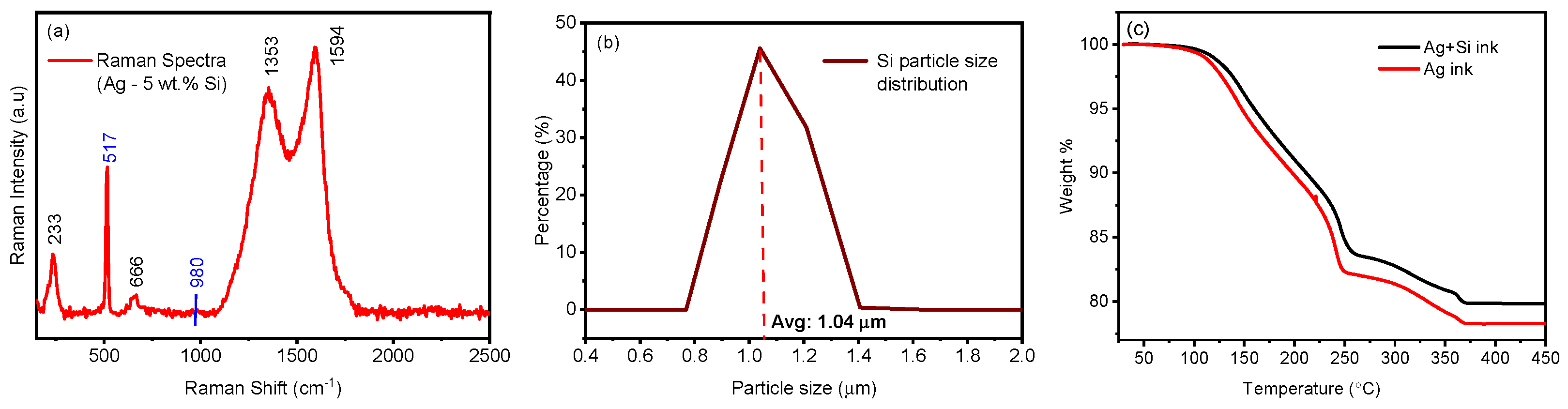
Figure 3.
SEM micrographs of a) pristine and b) modified () silver ink sintered at 250. c) EDX map of () ink sintered at 250 with particles highlighted in red.
Figure 3.
SEM micrographs of a) pristine and b) modified () silver ink sintered at 250. c) EDX map of () ink sintered at 250 with particles highlighted in red.
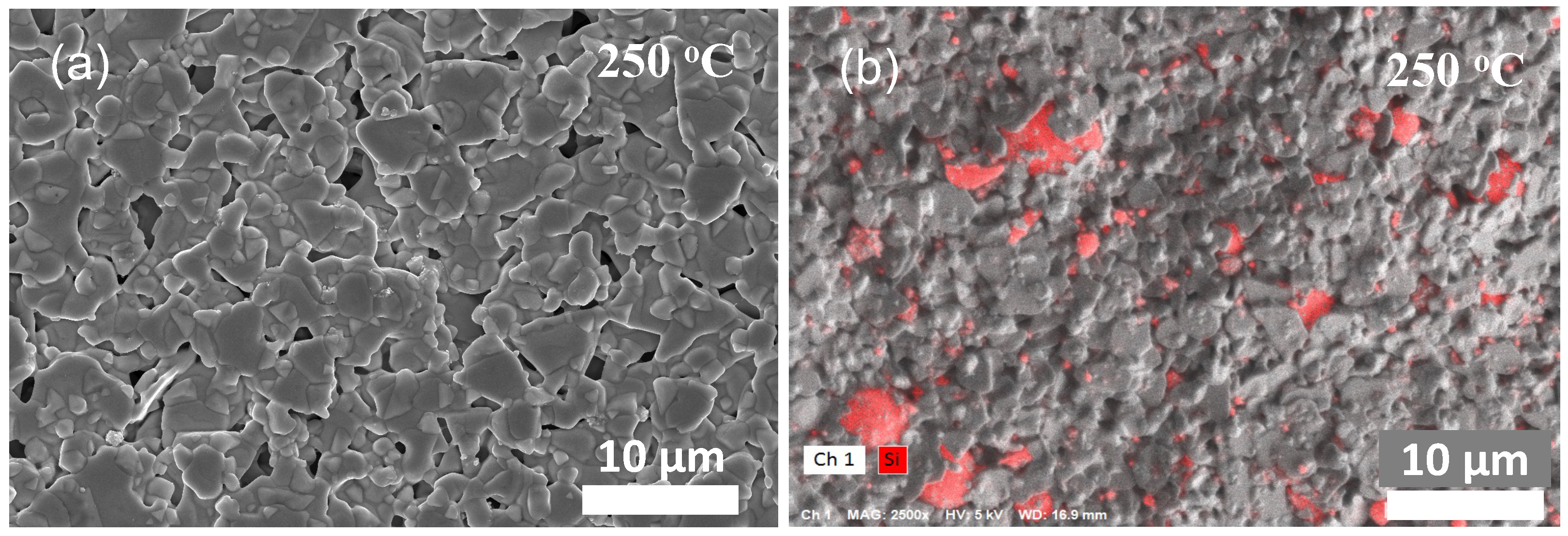
Figure 4.
Electrical conductivity of a) pristine and modified () inks with b) 3 wt.%, c) 5 wt.%, d) 7 wt.%, e) 10 wt.% silver inks treated at incremental temperatures for 1 hour isothermal exposure. Electrical conductivity of pristine and modified () inks thermally treated at f) 500, g) 500, h) 600, i) 700, j) 800, k) 900 over 10 mins, 1, 2, 3, 4 hours isothermal exposure.
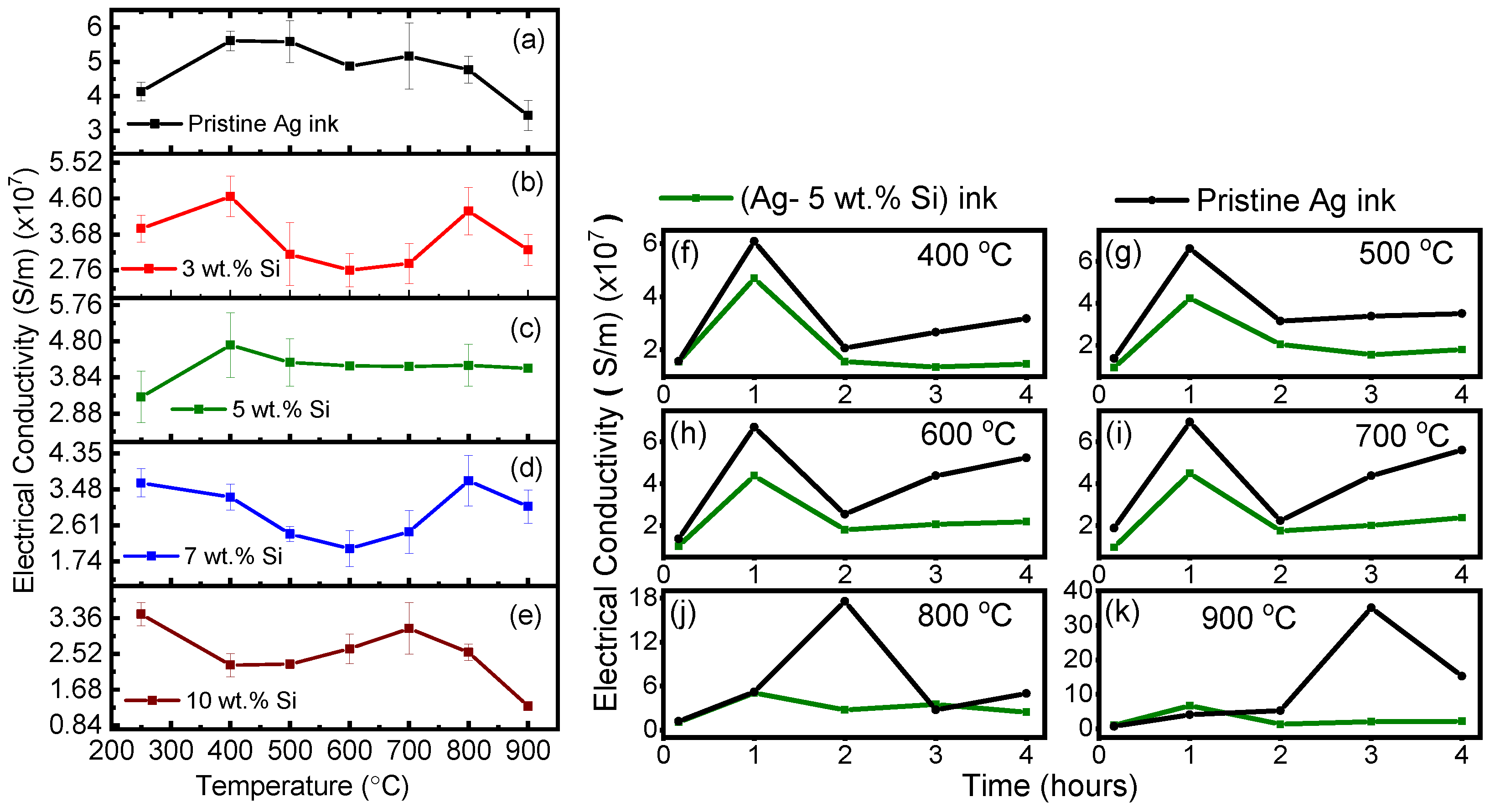
Figure 5.
Grain size evolution of pristine and modified () inks post thermal treatment between 250 and 900 for 10 mins, 1, 2, 3 and 4 hours.
Figure 5.
Grain size evolution of pristine and modified () inks post thermal treatment between 250 and 900 for 10 mins, 1, 2, 3 and 4 hours.
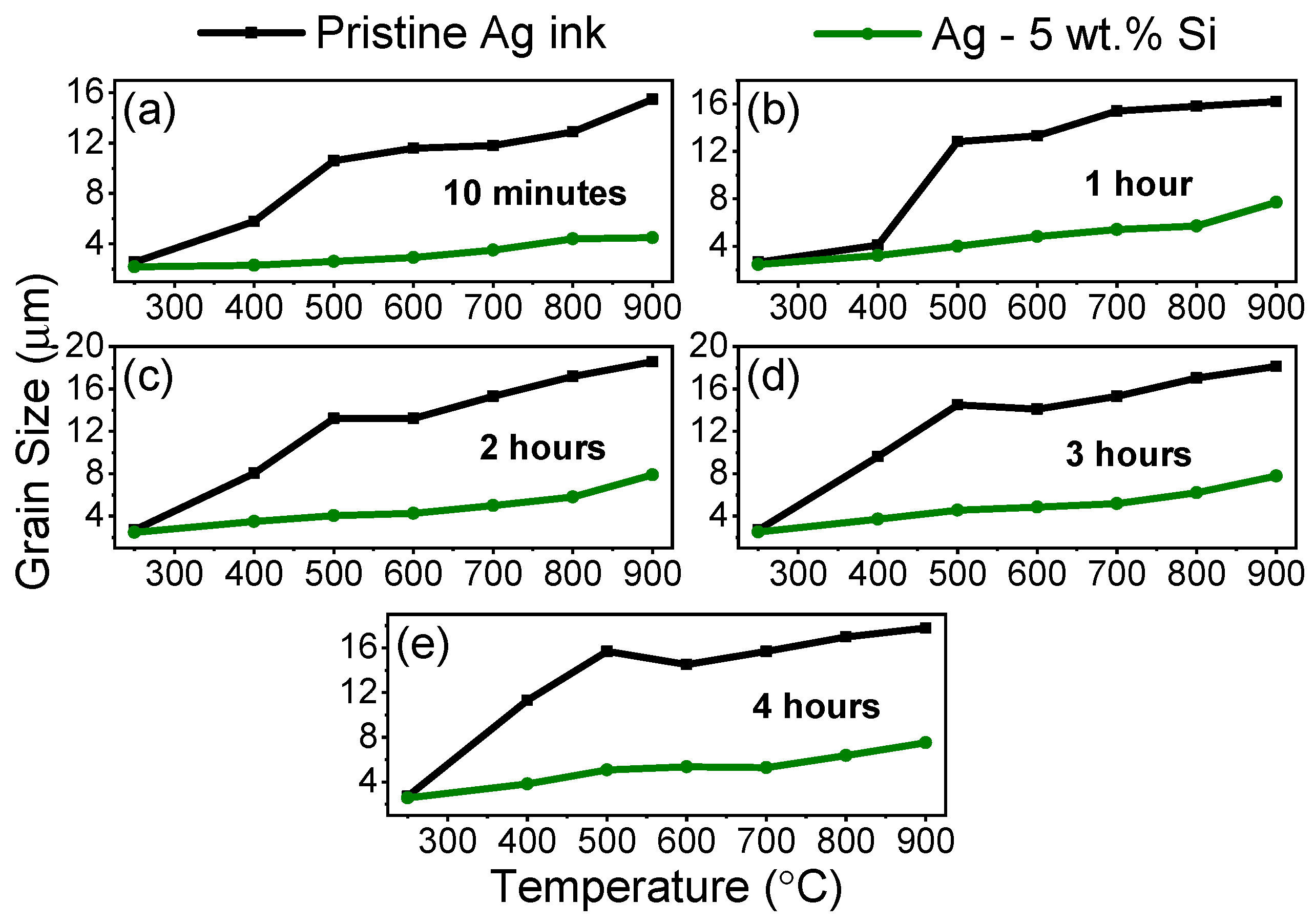
Figure 6.
SEM micrographs of pristine ink thermally treated at a) 400, b) 500, c) 600, d) 700, e) 800 and f) 900 for 1 hour.
Figure 6.
SEM micrographs of pristine ink thermally treated at a) 400, b) 500, c) 600, d) 700, e) 800 and f) 900 for 1 hour.
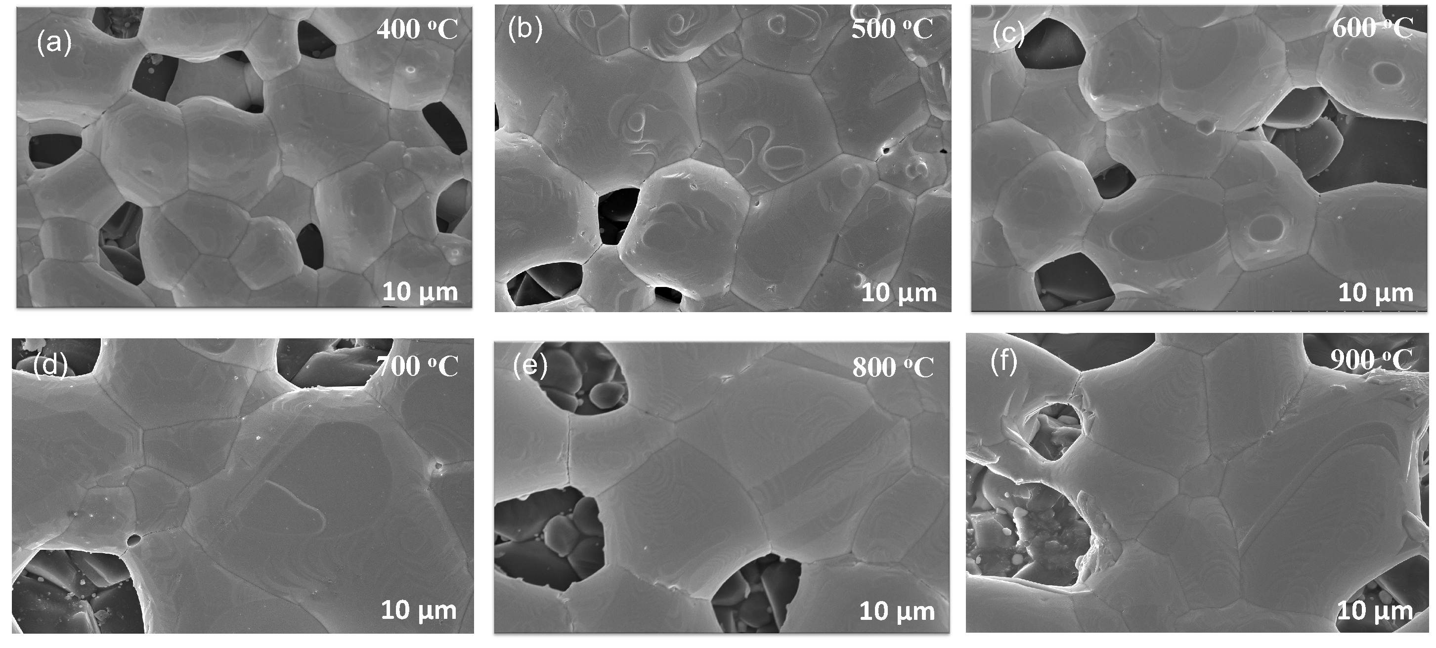
Figure 7.
EBSD micrographs of pristine ink thermally treated at a) 400, b) 500, c) 600, d) 700, e) 800 and f) 900 for 1 hour.
Figure 7.
EBSD micrographs of pristine ink thermally treated at a) 400, b) 500, c) 600, d) 700, e) 800 and f) 900 for 1 hour.
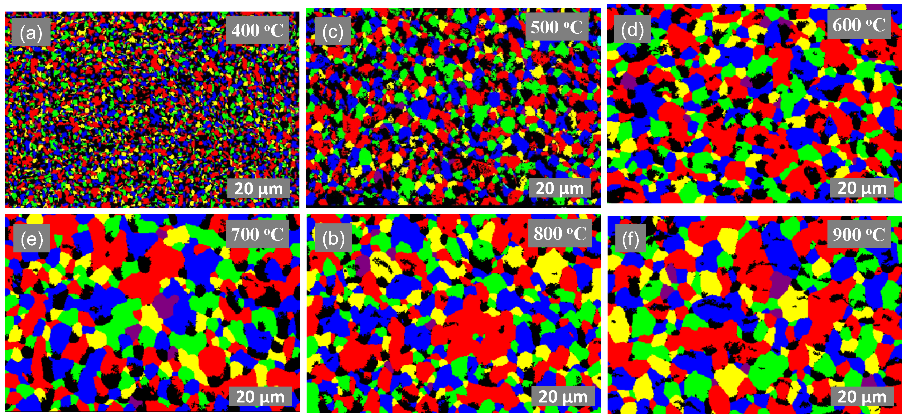
Figure 8.
SEM micrographs of 5 wt.% modified () ink thermally treated at a) 400, b) 500, c) 600, d) 700, e) 800 and f) 900 for 1 hour.
Figure 8.
SEM micrographs of 5 wt.% modified () ink thermally treated at a) 400, b) 500, c) 600, d) 700, e) 800 and f) 900 for 1 hour.
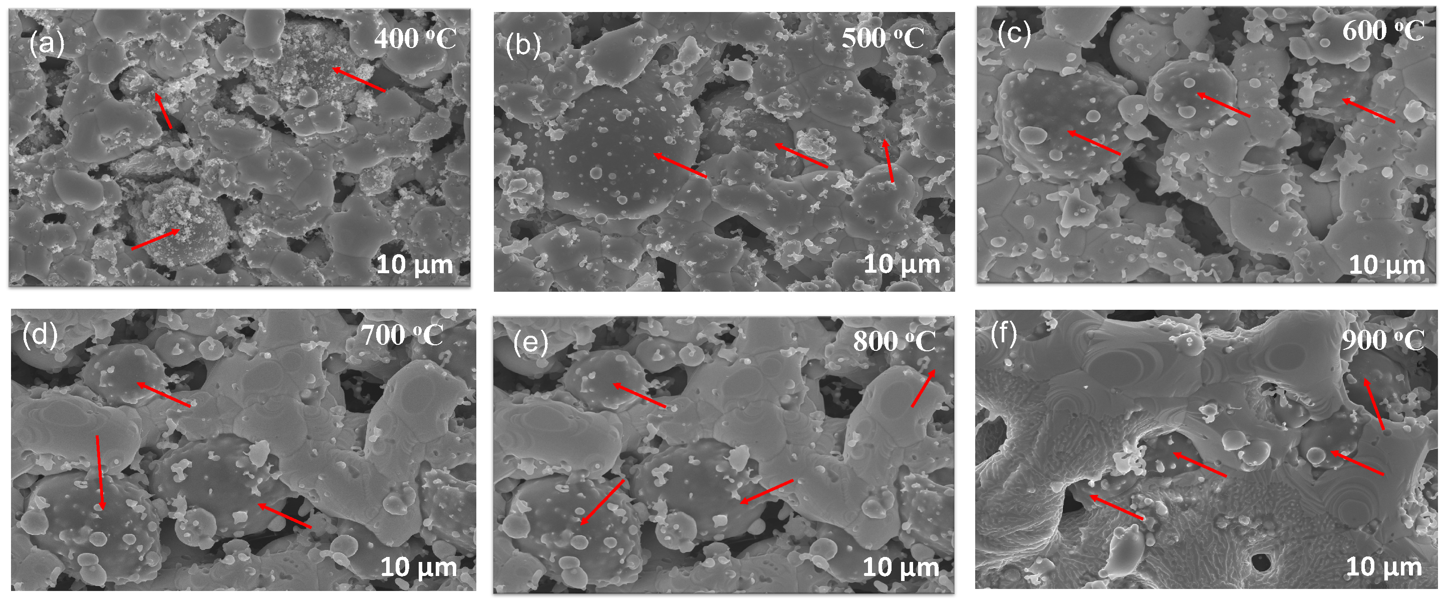
Figure 9.
EBSD micrographs of 5 wt.% modified () ink thermally treated at a) 400, b) 500, c) 600, d) 700, e) 800 and f) 900 for 1 hour.
Figure 9.
EBSD micrographs of 5 wt.% modified () ink thermally treated at a) 400, b) 500, c) 600, d) 700, e) 800 and f) 900 for 1 hour.
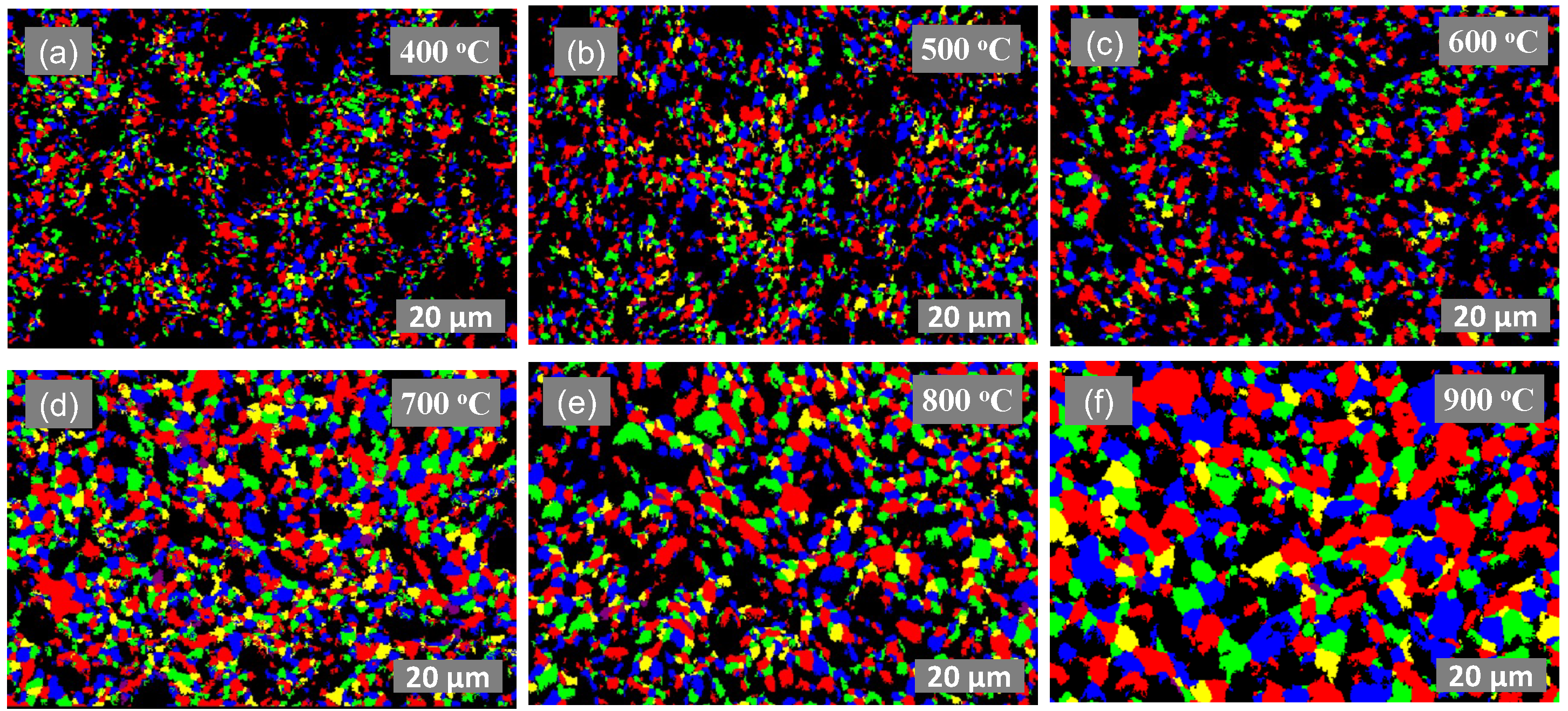
Figure 10.
SEM and EDX micrographs exhibiting the effect of a) and c) large particles and b) and d) smaller particles on the printed films morphology respectively.
Figure 10.
SEM and EDX micrographs exhibiting the effect of a) and c) large particles and b) and d) smaller particles on the printed films morphology respectively.
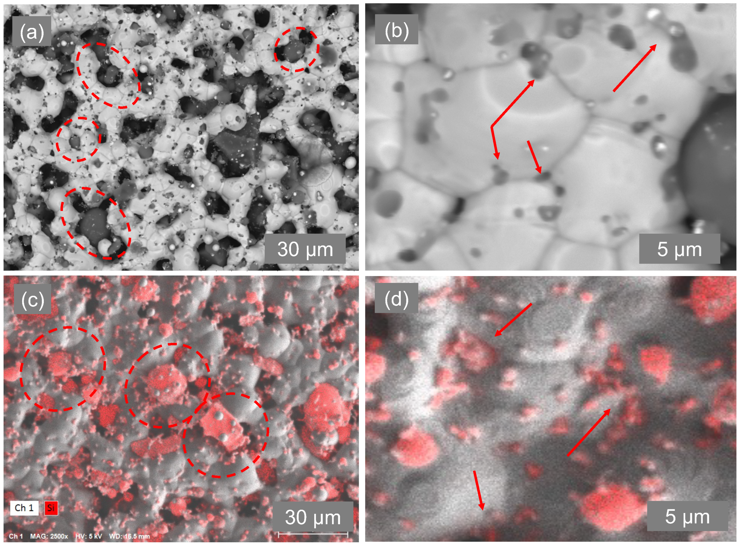
Figure 11.
XPS analysis of the silver ink samples after annealing. (a) % Oxygen concentration in silver oxide species for the pristine silver ink samples after a 3-hour isothermal annealing. (b) % Oxygen concentration in silver oxide species for the pristine silver ink samples after a 4-hour isothermal annealing. (c) % Oxygen in silicon oxide and total silicon oxide in the modified (Ag+Si) ink samples for 3 hour and 4 hour isothermal annealing.
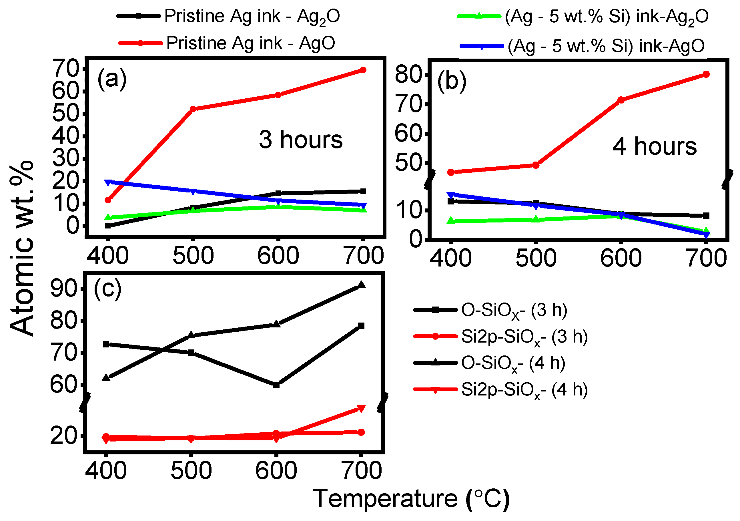
Figure 12.
Arrhenius plot of the parameter k versus isothermal exposure temperatures.
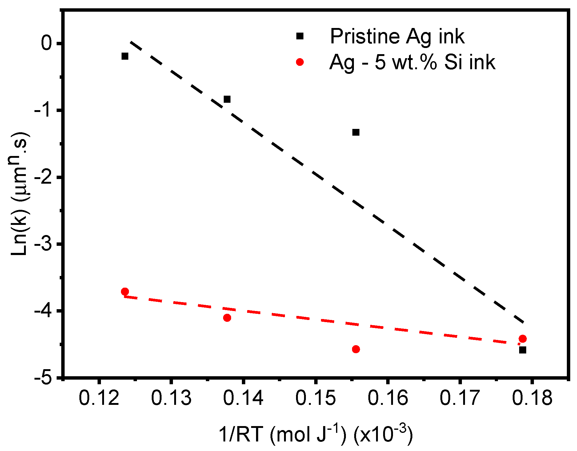

Table 1.
Calculations of n, k, activation energies (Q) and R values based on experimental results after 1 hour isothermal annealing at 400, 500, 600 and 700
Table 1.
Calculations of n, k, activation energies (Q) and R values based on experimental results after 1 hour isothermal annealing at 400, 500, 600 and 700
| Temperature | Ag only ink | (Ag-5 wt.% Si) ink | ||
|---|---|---|---|---|
| n | k | n | k | |
| 400 | 1.58 | 0.010 | 2.41 | 0.012 |
| 500 | 3.01 | 0.264 | 2.01 | 0.010 |
| 600 | 3.57 | 0.433 | 2.20 | 0.016 |
| 700 | 4.15 | 0.826 | 2.36 | 0.024 |
| Growth rate | Abnormal | Normal | ||
| Q (kJ mol) | 80.2 ± 19.15 | 38.52 ± 7.345 | ||
| R | 0.9 | 0.93 | ||
Disclaimer/Publisher’s Note: The statements, opinions and data contained in all publications are solely those of the individual author(s) and contributor(s) and not of MDPI and/or the editor(s). MDPI and/or the editor(s) disclaim responsibility for any injury to people or property resulting from any ideas, methods, instructions or products referred to in the content. |
© 2024 by the authors. Licensee MDPI, Basel, Switzerland. This article is an open access article distributed under the terms and conditions of the Creative Commons Attribution (CC BY) license (https://creativecommons.org/licenses/by/4.0/).
Copyright: This open access article is published under a Creative Commons CC BY 4.0 license, which permit the free download, distribution, and reuse, provided that the author and preprint are cited in any reuse.


