
Submitted:
11 July 2024
Posted:
12 July 2024
You are already at the latest version
Abstract
The work aims to develop an electromagnetic shielding measurement methodology and design an electromagnetic shielding effectiveness test setup for thin sheet material testing. In brief, multiple shielding effectiveness standards are described and analyzed in the thin sheet material testing framework. Two types of the developed shielding effectiveness test probe in high and low-frequency ranges are validated comprehensively. Extensive descriptions and data of developed testing methodology are also reported.
Keywords:
electromagnetic shielding
; shielding effectiveness
; test method
1. Introduction
Electromagnetic Interference refers to the disturbance or disruption of electromagnetic signals or radiation by other electromagnetic signals or sources. It occurs when the electromagnetic fields generated by one device or source interfere with the regular operation of another device. electromagnetic interference can result in various issues, including data corruption, signal degradation, malfunctions, or even complete failure of electronic devices or systems. electromagnetic interference can be caused by any number of sources for example electronic devices or their components, transmitters, lightning etc. As the number of devices are growing shielding them from the environment and shielding their generated interference is more important.
Increased intensity of research and development of new materials and their chemical, mechanical and electrical properties as well as search for their possible applications. One of the material types with potential to use in electromagnetic interference shielding is carbon polymer composites [1].
There are multiple standard methods available for measuring shielding effectiveness (SE) of the material such as MIL-DTL-83528G, IEEE 299.1-2013 and ASTM D4935-18 which have advantages and disadvantages which depend on the material type measured and intended use [2]. The flanged coaxial holder method in standard ASTM D4935-99 would be advantageous as the nano-carbon polymer composite material sample sizes are small.
For material electromagnetic shielding effectiveness measurements in a frequency range from 30MHz to 1.5GHz, an ASTM D4935-18 standard is used. ASTM D4935-18 standard describes shielding effectiveness measurement methodology for thin sheet materials using flanged coaxial holder ASTM. The advantage over free space measurement methods where large sheets of material are required is small diameter of only 10cm sample is needed which helps to reduce testing costs. The standard shielding effectiveness tester has multiple drawbacks, for example, the jig itself is expensive as the cost of raw material in combination with machining it. The ease of use is reduced as the tester itself weighs around 18kg and the standard itself is unclear on sizes of connection port [3]. Additionally devices increasingly operate at higher frequencies which requires different testing methodologies.
Other research has tried to overcome the shortcomings by decreasing the size of the tester in combination with different geometries which results in increased operating frequency up to 18GHz, reduced weight and smaller sample sizes [4,5,6,7]. In [8] mechanical changes in design were used to compensate discontinuities in taper section of the coaxial. [9] explores higher order circuit model for correction factor to eliminate resonance peaks of the measurements. Another alternative way of measuring shielding effectiveness is with TEM cells [10,11].
2. Theory and 3D Printed Shielding Effectiveness Tester Development
To overcome the stated shortcoming, we proposed and tested two designs of a 3D-printed shielding effectiveness tester. Both of the shielding effectiveness testers consists of two parts of flanged coaxial line with air dielectric, and where both of them have a N-type plug connectors.The first design is similar to the original ASTM standard tester made as proof of concept validation for 3D printed and laminated shielding effectiveness tester.The second shielding effectiveness tester coaxial flange part is reduced in size to increase the operating frequency of the tester.
2.1. Theory
Shielding effectiveness measures the amount which the signals passing through a shield is attenuated
Where is the transmitted power through a shielding material and is the power of the incident signal.
Shielding effectiveness can be further expressed by its components
where is absorption, is reflection and is multiple reflection, which is negligable. Measurements are usually done with a vector network analyzer (VNA), so it is useful to expand the shielding effectiveness in the terms of its S parameter data:
where R, T and A are reflection, transmission and absorption coefficients. , , are reflected, incident and transmitted signal intensities. In (5) the absorption coefficients are calculated proportionally to the incident signal. The signal strength inside the material itself is defined as , the effective absorption coefficient in relation to it:
And resulting components of shielding effectiveness in terms of logarithmic power:
For proper flanged coaxial shielding effectiveness measurement the system impedance must be 50 ohm’s which can be calculated from [12]
where D is outer conductor inner diameter and d is inner conductor diameter. In our case the dielectric is air which simplifies equation and impedance depends on dimensions of the coaxial. Coaxial transmission line primary work mode is transverse electromagnetic waves which upper frequency defines as [12]
where c speed of light.
2.2. Tester Development
Low frequency tester
The low-frequency shielding effectiveness tester consists of two parts of a flanged coaxial line with air dielectric. Signals are fed through an N-type plug panel mount coaxial connector. Internally, a transition from Teflon (or polyethylene) dielectric wave-guide to air dielectric coaxial is formed after the connector. After the dielectric type transition, the narrow coaxial transmission line gradually changes to a wider one where, at final dimensions, it maintains a 50 ohm impedance. The broader part of the coaxial is extended and terminated with a flange , allowing both sides to be connected and held together. The dimensions of the coaxial extension determine the highest measured frequency. For the first 3D printed prototype, the dimensions closely match the standard ASTM tester and the cutoff frequency is 1.75GHz
The shielding effectiveness test probe structure is shown on Figure 1. The diameter of the inner conductor at the base of the coaxial line with air dielectric is 5mm and the inner diameter of the outer conductor is 11.7mm, which provides 50 Ohm characteristic impedance, then it linearly extends to larger area coaxial maintaining 50 Ohm characteristic impedance with dimensions of 32.75mm inner and 76mm outer conductor. The total length of the tester for both parts is 356mm.
The shielding effectiveness tester main structure was 3D printed out of PLA to reduce cost, weight and verify feasibility of shielding effectiveness tester Figure 1. As the base of the print was oriented on the flanges which naturally are as flat as the printer heat bed the flat side tester halves were sanded as the printer is not accurate enough to allow the parts to fit very tightly together which is where signal leakage could occur. The inner conductive parts were laminated with 50 thick copper tape with conductive adhesive. End N-type panel mount connectors of the tester pressed in between sides and secured with screws, the center conductor is tightly pressed on the end of the connector centre conductor additionally the center is supported and held in place with foam ring. The specimen is inserted between the parts and secured by screwing it together with nylon bolts and nuts or compressing the two sections together with foldback clips as the area is enough to allow to use multiple strong foldback clips.
For characterization of the shielding effectiveness tester, it is necessary to create short circuit and matched or in this case empty circuits where no device under test is placed inside of tester. In a short-circuit, instead of the material sample, a well-conducting material is placed, such as a in our example a 0.5mm thick copper plate, which will create a short-circuit between the parts of the shielding effectiveness tester itself and the two VNA ports. A matched circuit would mean that the entire signal flows through perfectly and no signal attenuation is performed, this will be achieved by connecting the two parts of the shielding effectiveness tester together with no material inserted, paying attention to make the best possible contact between the two sections of the shielding effectiveness tester. As the created coaxial shielding effectiveness tester is not ideal the pass-through signal has some attenuation by itself and it is taken as the reference. The difference between S21 reference and S21 shorted will show the maximum dynamic range and the maximum measurable shielding effectiveness of the system. The measurements were made with ZNB20 2 port vector network analyzer the measurement system block diagram is shown in Figure 5. Both pass trough attenuation and copper plate short circuit is shown in Figure 2. The signal pass trough attenuation of the shielding effectiveness tester is about 0.7dB which means that no large obstructions are in the path of the signal in combination with short circuit measurement the system gives about 75dB dynamic range.
To analyse the quality of the structure in detail Tektronix DSA8200 digital serial analyser with 80E04 time domain reflectometry sampling module was used. Figure 2b show module in series with minicircuts 141-3SM+ cable which at point 1 connects to SMA plug to N-type jack adapter (1-2) where in which occurs the first dip of 42 .Part 2-3 is panel mount connector (Amphenol N6551A1-NT3G-50) which has good 50 impedance. The next dip of 40 at point 4 is the start of the taper which gradually smooths out as the dimensions get larger, at point 5 which is the end of the taper a small positive impedance jump is visible after that the coaxial line is about 51 OHM till the flange open end at point 6.
High frequency tester
Formula 10 shows that reducing the dimensions of the shielding effectiveness tester the transverse electromagnetic wave mode cutoff frequency increases, while using formula 9 dimensions can be found where coaxial line maintains 50 Ohm characteristic impedance. It is convenient to already use the existing properties of the N-type connector, where the interconnections internally form air coaxial transitions. By elongating these transitions and making a wider flange connection space, we create a similar shielding effectiveness tester layout as the previous one, but which works at higher frequencies.
At the base of the tester the inner coaxial conductor is a 3.18mm diameter rod with a 1.27mm diameter and approximately 10mm deep hole on one side, this hole is intended to connect the rod to the inner conductor of the N-type connector, after the hole a taper starts to a larger coaxial where the center conductors diameter reaches 5.77mm. The base of the outer conductor has a 8.31mm hole where the N-type jack to N-type plug adapter (Amphenol 172276), plug part is designed to screw on and create a continuous transition of the coaxial line. The inner conductors 3.18mm diameter with adapter outer conductor 7.32mm diameter forms an accurate 50 transmission line. After that the outer part tapers to 13.31mm which with 5.77mm inner conductor keeps 50.1 impedance. At the end the outer part of the tester expands to 30.48mm diameter flange for material testing.
Similar as the low frequency tester the high frequency tester was fabricated using the 3D printer. As the parts dimensions are smaller inaccuracies have higher impact on final transmission line impedance’s to mitigate it the nozzle of the printer was reduced to 0.2mm. Same as the low frequency tester the each side consists of two lobes which before copper tape lamination were sanded to ensure tight fit. The center conductor is held in place with 3D printed ring. This smaller test mock-up will allow testing of materials up to approximately 10GHz frequency, with a smaller sample of material to be used, which facilitates and simplifies the testing of new materials. Using less material is beneficial for testing more expensive or difficult to obtain materials.
To determine the quality of produced shielding effectiveness tester prototype its scatter parameter were taken when there are no material present and with 0.5mm copper plate. The signal passtrough attenuation up to 6GHz is relativeley small reaching only 2dB, in frequency region from 6 to 8GHz the increase in attenuation is larger reaching 5.6dB. Meanwhile the the measurement with double sided FR4 board signal attenuation reached 78-82dB which gives the aproximate dynamic range of about 70dB visible in Figure 4a.
Figure 4b time domain reflectometry shows again that the SMA to N-type plug connector point 1-2 has a 40 dip. After that the N-type jack to plug adapter part in points 2-3 of the tester has 50 ohm impedance. After the adapter the narrow part of the coaxial line starts with lower impedance which reaches the lowest point at the start of the taper in point 4 where it drops to 40 . In the middle of the taper points 4-5 the impedance reaches 50 and lowers at the end of ti at point 5. Trough out rest of the coaxial line the impedance is not stable dipping and rising until the end of the tester at point 6. Part of why the impedance are lower would be explainable by the actual applied tape layer thickness and the end print properties. As the print is not exactly level but has a ribbed relief from print layer structure and the applied tape sits on top of the layer ribs as well as in some places there are multiple layer of tape in which case the clearance is reduced further and these differences in dimansions on smaller device leads to larger differences in impedance mismatch causing lower impedances on avarage.
3. Measurements
3.1. Materials
To test the developed shielding effectiveness measurement devices three materials were used. 1st material was a 3D printed standard black PLA filament (Verbatim 55318) sheet with thickness of 0.6mm. As the plastic is dielectric the signal should have no problem passing trough and the attenuation should be low. 2nd material used was a conductive 3D filament (Conductive Filaflex 60AFBLACK175500) sheet with thickness of 0.6mm. This material should have some attenuation as it is conductive. 3rd material chosen was a sprayable graphite coating (Kontakt chemie KOC-GRAPHIT33/200) designed to be used as a EMI shield. Coating was sprayed on a paper sheet (NAVIGATOR UNIVERSAL A4 80g/m2, Art. Nr. 006102). Paper thickness is 100 on which 8 layers of graphite was sprayed after which the it was baked in 140C for 60 minutes resulting in graphite thickness of 50 .
3.2. Measurement Setup
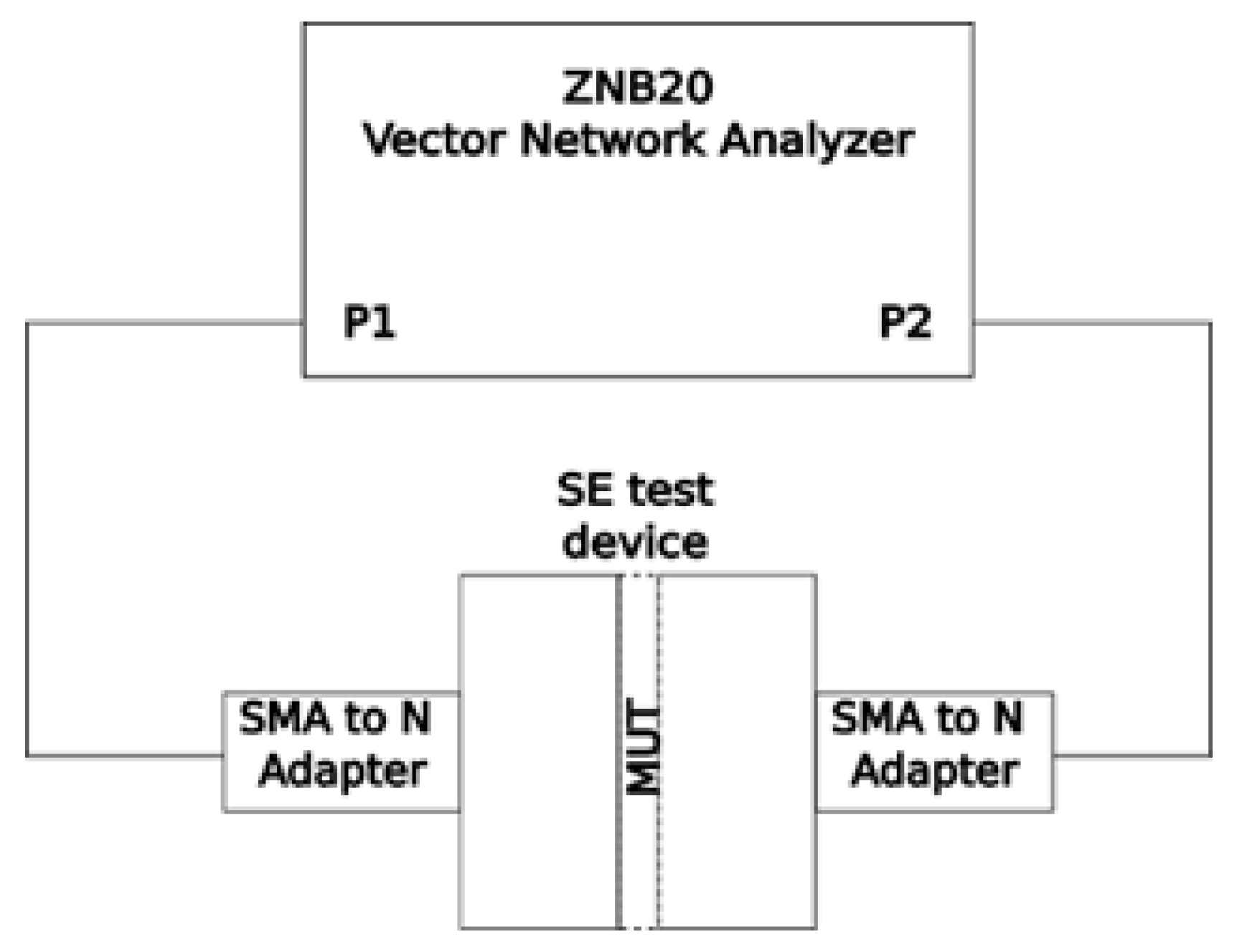
Shielding effectiveness measurement diagram is shown in Figure 5 where both ports of the vector network analyzer are connected to ADT-2735-FF-3MM-02 adapter which connects to 141-MSM+ coaxial cable which trough SMA to N-type adapter connects to shielding effectiveness tester. Before measuring material samples, it is necessary to carry out calibration, which will ensure that defects of the measurement system are compensated. Calibration was carried out from VNA up to ends of coaxial cables where the shielding effectiveness test devices are connected.
Figure 5.
Shielding effectiveness measurement system block diagram.
Full shielding effectiveness evaluation in terms of ASTM standard and therefor in our case consists of reference measurement and load measurement where reference is the same material as load material. Shielding effectiveness result is equal to reference measurement minus load measurement. Dimensions of reference measurement shown in Figure 6 where both low frequency setup and high frequency setup reference specimen dimensions are shown. The high frequency reference specimen Figure 6 top is the same as the flange connecting face area which is disc with outer diameter of 30.48mm and inner diameter of 13.31 and a center circle with diameter of 5.77mm. Load specimen is a circle which covers all of the flange area has a mounting holes. The low frequency reference specimen Figure 6 bottom center circle is with area of 32mm but the outside is a square shape with circle cutout. The Square is 100mm by 100mm with both reference and load having a mounting holes.
4. Results and Discussion
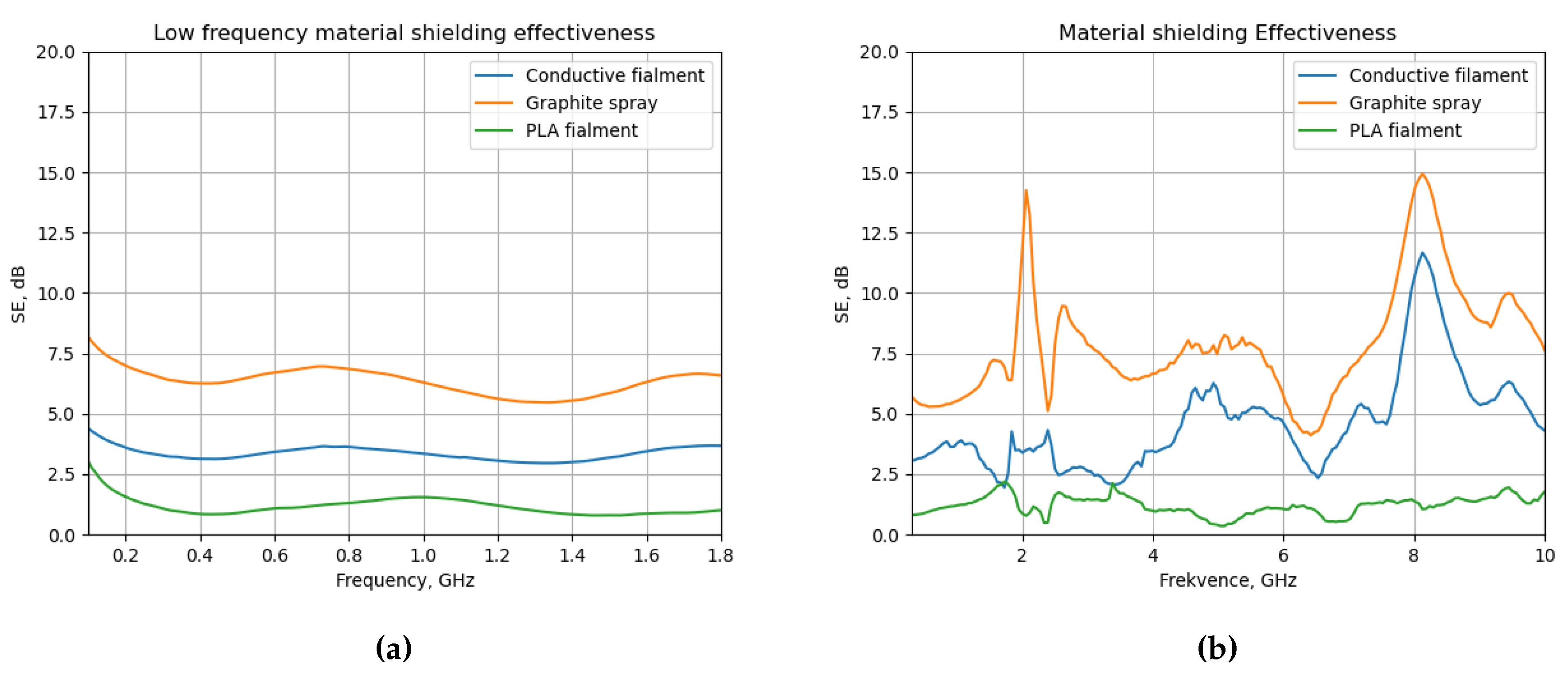
The results of the low frequency measurements are shown in Figure 7a where PLA plastic sheet shows about 1-2dB attenuation trough out the frequency range from 30MHz to 1.5GHz. The Conductive filament sheet shows shielding effectiveness of 3-5dB trough out the frequency range. The graphite paper shows shielding effectiveness of 7.5-7dB attenuation in lower frequency range up to 1GHz and weakens gradually to 6-7 dB attenuation.
The results of the high frequency measurements are shown in Figure 7b where PLA sheet material shows about 0.5-2dB attenuation. At low frequencies up to 1.8GHz peaking and at 5 GHz dipping to 0.5dB then there is a gradual increase in attenuation to 2dB with some peaking and dipping. The 2nd conductive filament material sheet has 3 to 4dB attenuation up until 4GHz after that increases to 5-6dB up to 6GHz dropping to 2.5dB at 7GHz and at 8.2GHz seems to have a resonance which increases the attenuation to 11dB.
The high-frequency tester demonstrator was 3D printed with PLA material using the 0.2 mm print nozzle, which leaves 3D print artifacts that require additional precise smoothing, additionally, multiple layers of copper tape are required to cower, specifically the cone-shaped places at the taper part which further introduces inaccuracies that could explain Figure 4 no material high passthrough signal attenuation and time domain reflectometry impedance spikes, ass well as the Figure 7b with similar characteristics in conductive filament and graphite shielding effectivenes measurement. 3D print artifacts, along with the following disadvantages, could be possibly avoided by using a stereolithography-based resin 3D printer and electro-plating to achieve a conductive surface where the electroplated surface needs to be from a developed conductive material, which can be achieved by mixing conductive particles in the resin or spraying the surface with graphite spray or another method.
5. Conclusions
A low-frequency shielding effectiveness tester with an operating frequency of up to 1.8GHz was designed and constructed using highly accessible methods with 3D printing and lamination with copper tape, and its parameters were measured. A detailed description of the design was included. Successful validation of a low-frequency tester allowed us to go further with the design of a high-frequency shielding effectiveness tester where a benefit is the minor sample size requirement. The tester uses properties of N-type connectors. The coaxial air transition part was extended and made the larger area, and the theoretical working frequency increased to 10GHz. The high-frequency tester parameters were measured, and the operation was validated with three different materials.
Author Contributions
Conceptualization, E.L. and G.S.; methodology, E.L. and G.S.; validation, G.S.; formal analysis, E.L. and G.S.; investigation, E.L. and G.S.; resources, G.S.; writing—original draft preparation, E.L.; writing—review and editing, E.L. and G.S. visualization, E.L.; supervision, G.S.; project administration, G.S. All authors have read and agreed to the published version of the manuscript.
Funding
This research was funded by the Latvian State Research Program for Defense Innovation, project “Enhanced electromagnetic protection and cybersecurity through field-deployable innovative shielding, monitoring and data destruction technologies”, Nr. VPP-AIPP-2021/1-0007.
Institutional Review Board Statement
Not applicable
Data Availability Statement
The data presented in this study are available on request from the corresponding authors.
Conflicts of Interest
The authors declare no conflict of interest.
References
- Chen J, Liu B, Gao X, Xu D. A review of the interfacial characteristics of polymer nanocomposites containing carbon nanotubes. RSC Adv. 2018;8(49):28048-28085. [CrossRef]
- P. F. Wilson and M. T. Ma, "Techniques for measuring the electromagnetic shielding effectiveness of materials. II. Near-field source simulation," in IEEE Transactions on Electromagnetic Compatibility, vol. 30, no. 3, pp. 251-259, Aug. 1988. [CrossRef]
- Vasquez, Horacio, Espinoza, Lesly, Lozano, Karen, Foltz, Heinrich, Yang, Shuying. (2009). Simple device for electromagnetic interference shielding effectiveness measurement. IEEE EMC Society Newsletter.
- Chaochan Chen and Yu Sang, "The development of novel coaxial tester on electromagnetic shielding effectiveness measurement," 2015 IEEE 6th International Symposium on Microwave, Antenna, Propagation, and EMC Technologies (MAPE), Shanghai, China, 2015, pp. 506-510. [CrossRef]
- A. Tamburrano, D. Desideri, A. Maschio and M. Sabrina Sarto, "Coaxial Waveguide Methods for Shielding Effectiveness Measurement of Planar Materials Up to 18 GHz," in IEEE Transactions on Electromagnetic Compatibility, vol. 56, no. 6, pp. 1386-1395, Dec. 2014. [CrossRef]
- R. Valente, C. De Ruijter, D. Vlasveld, S. Van Der Zwaag and P. Groen, "Setup for EMI Shielding Effectiveness Tests of Electrically Conductive Polymer Composites at Frequencies up to 3.0 GHz," in IEEE Access, vol. 5, pp. 16665-16675, 2017. [CrossRef]
- Y. K. Hong, C. Y. Lee, C. K. Jeong, D. E. Lee, K. Kim, J. Joo; Method and apparatus to measure electromagnetic interference shielding efficiency and its shielding characteristics in broadband frequency ranges. Rev. Sci. Instrum. 1 February 2003; 74 (2): 1098–1102. [CrossRef]
- C. C. Chen, F. M. Lu, Yu-Sang and Qing-Cai, "A compensated flanged coaxial tester for shielding effectiveness measurement," 2012 International Conference on Microwave and Millimeter Wave Technology (ICMMT), Shenzhen, China, 2012, pp. 1-3. [CrossRef]
- M. S. Sarto and A. Tamburrano, "Innovative test method for the shielding effectiveness measurement of conductive thin films in a wide frequency range," in IEEE Transactions on Electromagnetic Compatibility, vol. 48, no. 2, pp. 331-341, May 2006. [CrossRef]
- V. Voicu, I. Pătru, L. -A. Dina, P. -M. Nicolae and I. D. Smărăndescu, "Shielding effectiveness evaluation using a non-standardized method," 2017 International Conference on Electromechanical and Power Systems (SIELMEN), Iasi, Romania, 2017, pp. 208-211. [CrossRef]
- H. A. Wolfsperger, H. Strehlow and A. J. Schwab, "A new dual-coaxial-TEM cell," 1999 International Symposium on Electromagnetic Compatibility (IEEE Cat. No.99EX147), Tokyo, Japan, 1999, pp. 528-531. [CrossRef]
- David M. Pozar., Microwave Engineering, 4th Edition,4th ed; Wiley, November 2011; pp. 51–134.
- Bleija, M.; Platnieks, O.; Macutkevič, J.; Banys, J.; Starkova, O.; Grase, L.; Gaidukovs, S. Poly(Butylene Succinate) Hybrid Multi-Walled Carbon Nanotube/Iron Oxide Nanocomposites: Electromagnetic Shielding and Thermal Properties. Polymers 2023, 15, 515. [Google Scholar] [CrossRef] [PubMed]
Figure 1.
Design of developed low frequency shielding effectiveness tester where (a) tester technical drawing and (b) top finished tester, bottom laminated assembly parts
Figure 1.
Design of developed low frequency shielding effectiveness tester where (a) tester technical drawing and (b) top finished tester, bottom laminated assembly parts
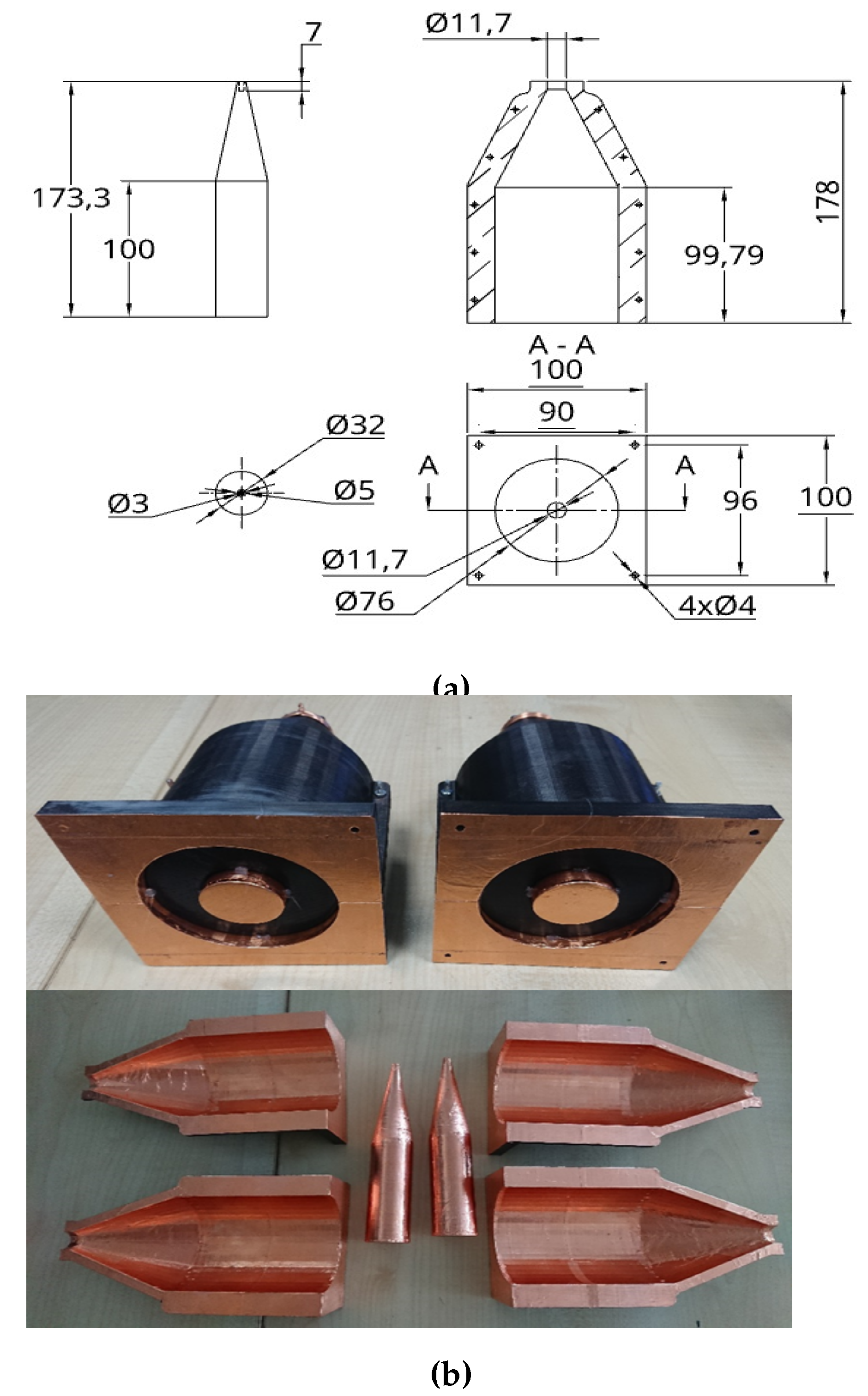
Figure 2.
Developed low frequency tester parameters where: (a) S21 of passtrough signal without material and with 0.5mm copper plate S12; (b) Time domain reflectometry data
Figure 2.
Developed low frequency tester parameters where: (a) S21 of passtrough signal without material and with 0.5mm copper plate S12; (b) Time domain reflectometry data
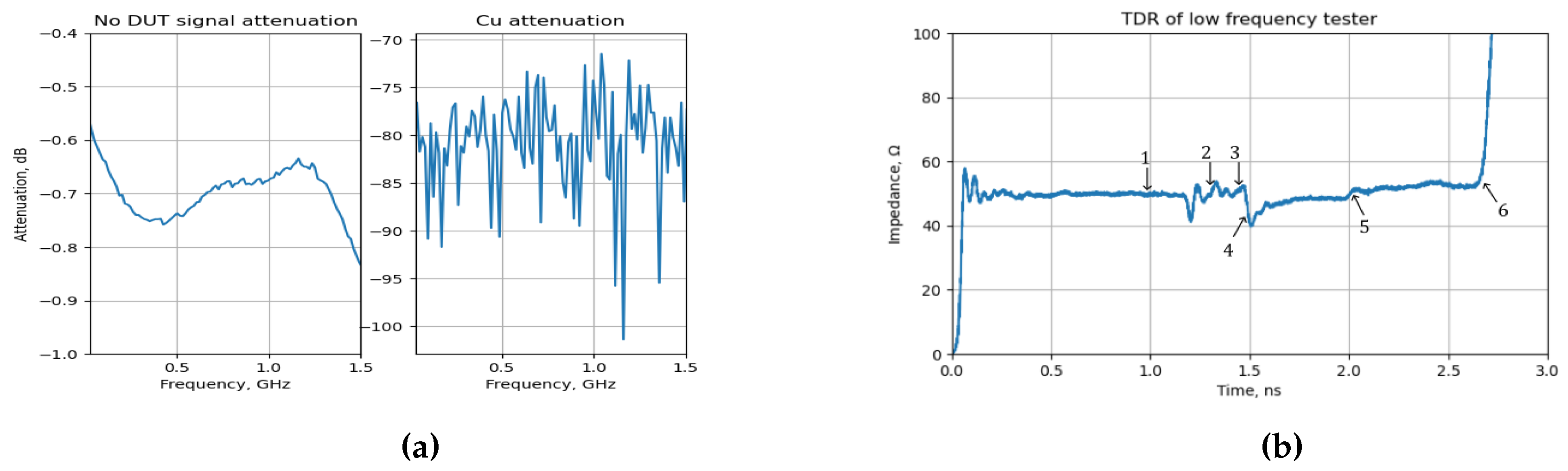
Figure 3.
Design of developed high frequency shielding effectiveness tester where: (a) tester technical drawing; (b) finished assembly of the tester
Figure 3.
Design of developed high frequency shielding effectiveness tester where: (a) tester technical drawing; (b) finished assembly of the tester
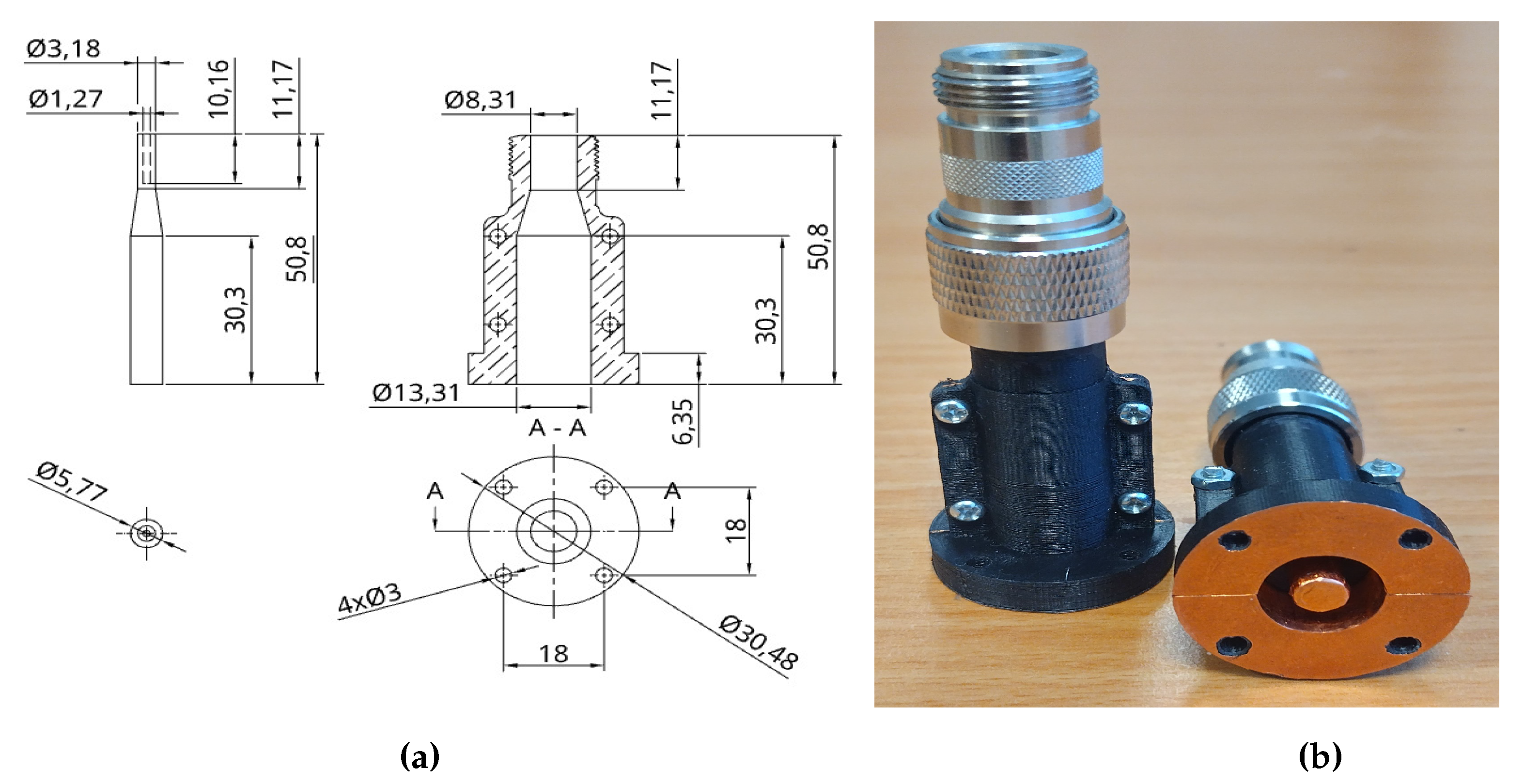
Figure 4.
Developed high frequency tester parameters where: (a) S21 of passtrough signal without material and with 0.5mm copper plate S12; (b) Time domain reflectometry data.
Figure 4.
Developed high frequency tester parameters where: (a) S21 of passtrough signal without material and with 0.5mm copper plate S12; (b) Time domain reflectometry data.
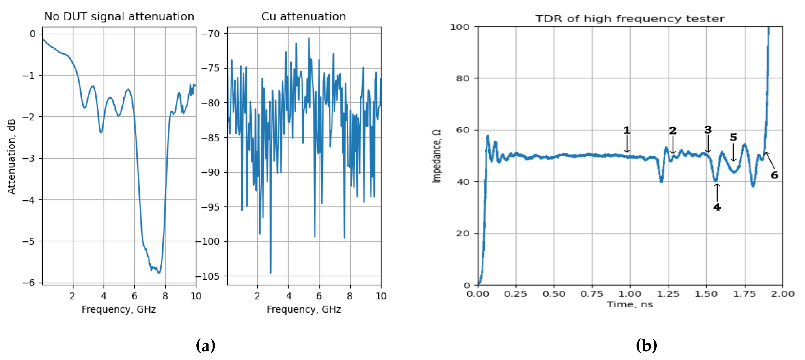
Figure 6.
Reference and load specimen dimensions top for high frequency setup, bottom for .
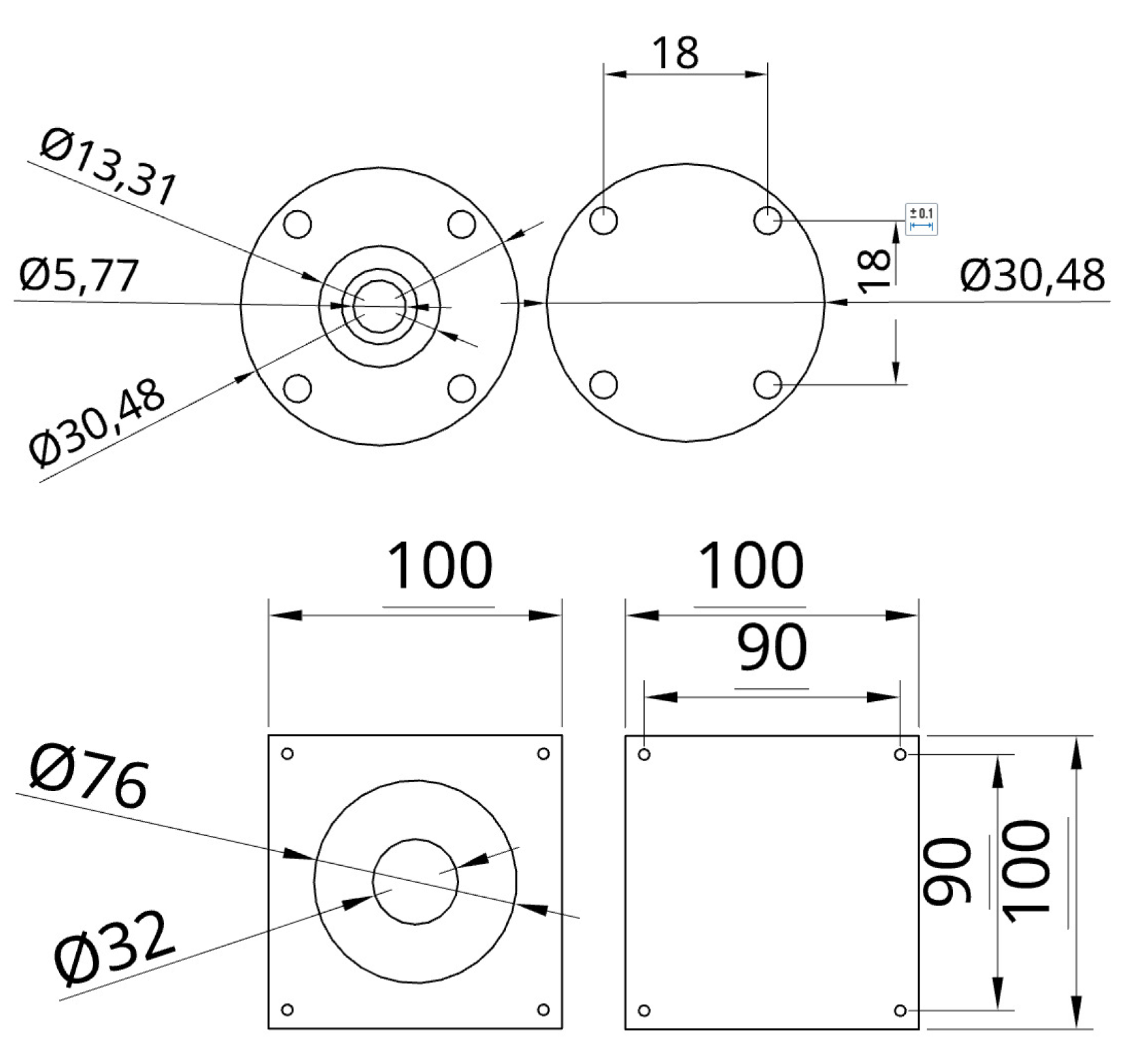
Figure 7.
Measured material results where: (a) Low frequency shielding effectiveness tester results; (b) High frequency shielding effectiveness tester results.
Figure 7.
Measured material results where: (a) Low frequency shielding effectiveness tester results; (b) High frequency shielding effectiveness tester results.
Disclaimer/Publisher’s Note: The statements, opinions and data contained in all publications are solely those of the individual author(s) and contributor(s) and not of MDPI and/or the editor(s). MDPI and/or the editor(s) disclaim responsibility for any injury to people or property resulting from any ideas, methods, instructions or products referred to in the content. |
© 2024 by the authors. Licensee MDPI, Basel, Switzerland. This article is an open access article distributed under the terms and conditions of the Creative Commons Attribution (CC BY) license (http://creativecommons.org/licenses/by/4.0/).
Copyright: This open access article is published under a Creative Commons CC BY 4.0 license, which permit the free download, distribution, and reuse, provided that the author and preprint are cited in any reuse.


