Submitted:
13 May 2024
Posted:
13 May 2024
You are already at the latest version
Abstract
In this paper, single and repetitive frequency UIS characteristics of 1200 V asymmetric (AT)and double trench silicon carbide (DT-SiC) metal–oxide-semiconductor field-effect transistors (MOSFETs) under different working conditions are investigated by experiment and simulation. For asymmetric trench SiC MOSFETs, the failure mode is all thermal runaway under working conditions. However, the failure mode of double trench SiC MOSFETs mostly is gate oxide rupture, which indicates an instable avalanche robustness under UIS stress. The variations of measured parameters are recorded to evaluate typical electrical features of device failure. Furthermore, TCAD simulation is used to reveal the electro-thermal stress inside the device during avalanche. Additionally, failed devices are decapsulated to verify the location of failure point from the perspective of the semiconductor die. Finally, a new type of stepped-oxide vertical power DT MOSFET with P-type shielding and current spread layers is proposed for improvement of gate dielectric reliability.
Keywords:
SiC Trench Power MOSFET
; UIS
; Failure analysis
; Optimized structure
1. Introduction
Due to the wide bandgap, high-critical breakdown electrical field, and thermal conductivity, SiC has been well established as the most promising candidate for high-temperature and high-power applications.
Because of intrinsic SiO2 as gate dielectric, SiC vertical power MOSFET possess simultaneously the advantage of high speed and high power making them widely applied in switch power markets such as photovoltaic inverters, electric vehicles, electric aircraft, uninterruptible power supplies, and energy distribution networks which a high dv/dt and di/dt [1] could be generated during high speed switching. If the inductive load such as motor, inductor is used, when the turn-on and turn-off switches speedly , due to the variation of the current flowing through the load inductor can not track synchronizely the one in loop, an induced voltage will be generated and stressed between the drain and source of the DUT. If the induced voltage exceeds the avalanche voltage of devices, the devices will be forced into avalanche mode. The stored energy in load inductor during the conduction of loop will be released through the power devices at the moment of turn-off. High voltage and large current will simutaneosly stress on the devices leading to devices likely failure [2,3,4].
Up to now, many researches have focused on UIS phenomena of planar MOSFET, It is generally believed that there are two possible reasons for single UIS failure of the device [5,6,7,8,9,10,11,12,13,14,15,16]: one is the turn-on of parasitic BJT triggering positive thermal-electrical feedback, ultimately leading to device failure. and the other is high junction temperature causes the aluminum metal to melt, resulting in device failure. As to repetitive UIS failure mechanism, it is commonly believed that hot hole in JFET region will be injected into oxide and trapped by the interface states and gate oxide leading to the parameters degradation. However, there are fewer comprehensive studies [17,18,19] on UIS failure mechanisms research including temperature characteristics, some important circuit loop parameters under single and repetitive UIS stress on trench gate MOSFET.
In this paper, a comprehensive of single and repetitive frequency UIS characteristics of 1200V AT-MOSFET and DT-SiC MOSFETs under different working conditions are investigated by experiment and simulation. i.e Rohm DT-MOSFET and Infineon AT-MOSFETs with the same current rate and on-state resistance. The single pulse UIS and repetitve UIS measurements were performed on these two kinds of devices.Degradation and failure mechanisms of devices have been researched by combination of measured datas and numerical simulation and microstructure analysis. A reasonable physical failure explanation during avalanche has been given. Additionally, failed devices are decapsulated to verify the location of failure point from the perspective of the semiconductor die. Finally, a new type of vertical power DT MOSFET is proposed for the improvement of gate dielectric reliability.
2. Device Structures and Experimental Setup
The measurements are done on devices under test (DUTs)listed SCT3080 shown in Figure 1(a) as a symmetrical double-trench SiC MOSFET rated at 4.2V,30 A, 1200 V, 80 mΩ with area 2.4mm*3.0mm and IMZ120R090M1HXKSA1 in Figure 1(b) as an asymmetrical trench SiC MOSFET rated at 4.5V,26 A, 1200 V, 90 mΩ with area 2.2mm*2.1mm, all encapsulated in TO-247-3 packages.
Figure 2 shows the circuit diagram(a) and wave curves diagrams(b). Figure 2(c) shows the image of UIS test setup. The main circuit includes two parts: driver circuit and power loop. The driver circuit is composed of driver source, gate resistance RG, and the DUT. The power loop includes a DC voltage source VDD, a DC stabilizing capacitor CDC, a load inductor L, and the DUT. Both of DUT and Si IGBT acts as charging switch to control load inductor L. Si IGBT will isolate DUT from DC bus. In this circuit, when IGBT module and VG turns off simultaneously, it ensures that DC bus does not participate in energy dissipating during avalanche events. During the whole measurement, VDD could be set much higher than the avalanche voltage of DUT, thus the conduction time can be decreased and thereby helps to reduce heat generation.
Figure 2.(b) gives the waveform diagrams, BVDSS is avalanche voltage, t3-t2 is avalanche time tav, t2-t1 is charging time of load inductor. The dc power supply voltage is set to be 50 V. Gate voltage is switched from -3 to +15V, several 20Ω resistors are parallelly connected between gate driver and MOSFET, the load inductor is chosen to be 3mH. Seeing from the Figure 2(a) and waveforms in Figure 2(b), When the IGBT and DUT turn on at the same moment, the current flowing through the inductor increases linearly. When the pre-set maximum current value is arrived, the energy stored in inductor force DUT to enter avalanche mode simultaneously when the DUT turns off.
3. Parameters Degradation and Avalanche Ruggedness Analysis
A. Single UIS Test
Figure 3 and Figure 4 show the typical single UIS waveforms of AT-MOSFET and DT-MOSFET at the last test before failure (Figure 3) and at failure (Figure 4) under 3.0mH inductive load conditions, respectively. When MOSFET turns ON, the IDS rises linearly to the maximum drain-source current (IDS, Max) with a slope of VDD/L. After it turns OFF,the energy stored in inductive load forces the MOSFET to enter into avalanche mode. While at this moment the VDS mantains breakdown voltage and IDS gradually decreases to zero from IDS, max. For AT-MOSFETs, the peak drain current and the voltage across the drain to source is 18 A and 1820 V during avalanche, respectively, avalanche state lasts for 32.48 us, while the gate pulse width reaches 1.08ms. Avalanche energy is 0.53J. When avalanche occurs, as shown in Figure 4(b), the gate pulse width increase to 1.14ms, the peak drain current increase to 19A and avalanche voltage remains 1820 V, the avalanche time lasts for 18.45us, then, the DUT fails which means that the blocking capability is lost between source and drain. Comparatively, for DT-MOSFETs, before failure, the avalanche current and voltage is respectively 17A and 2280V, avalanche state lasts for about 24.29us and gate pulse width reaches 1.02ms. Avalanche energy is 0.47J. When avalanche occurs, the current reaches to 18A, and gate pulse width arrives to 1.08ms, while the avalanche state lasts only for 30.45ns because of longer gate pulse width than the one before failure. In Figure 4 (a) and (b), because of IGBT module protection as marked with black arrow, thermal away doesn’t occure in our test, current increasement is shut-down by the turn-off of IGBT module.
Table 1 presents the IDS,Max, VDS,max, EAV and tAV of the DUTs under single UIS test with different inductive loads. We can see from this table that the avalanche withstand capability gradually increases with the increase of inductor. The peak avalanche current presents a decreasing trend, while the avalanche duration gradually increases.
The EAV of AT-MOSFET is higher than that of DT-MOSFET, which means superior single UIS ruggedness than SiC MOSFETs with AT structure. Also, higher EAV indicates serious thermal stress in SiC MOSFET, so the avalanche voltage of 2240V makes DT-MOSFET more susceptible than AT-MOSFET to gate oxide reliability.
Figure 5 gives the dependence of tAV and EAV on on-state time ton for both AT-MOSFET(a) and DT-MOSFET(b) with a fixed load inductor value. All measurements dates are recorded before the DUT failure occurs. From Figure 5(a) and 5(b), we can see that tav and Eav increasing with the increasement of ton and almost the same the variation trend of curves with temperature.
Figure 6 presents the dependence of tav and Eav for DT- and AT- SiC MOSFETs on ambient temperature with load inductor equals to 3mH in the UIS conditions. For these two types of transistors, a different variation with temperature is observed. For AT-MOSFET, tav and Eav decreases a little bit with the temperature increasing. From 25℃ to 175℃, the maximum tav has decreased by approximately 3% and the maximum Eav has decreased about 6%. While for DT-MOSFET, comparatively, as the ambient temperature increases, both of tav and Eav increases monotonically. From 25℃ to 175℃, tav has increased by approximately 7% and the maximum Eav has increased significantly 26%. So, the temperature has a significant impact on the avalanche energy of DT MOSFET.
Figure 7 shows the peak avalanche current (Ipeak)、start point of avalanche voltage(BVst) and peak avalanche voltage(Vpeak) at failure of DT MOSFET and AT MOSFET with a fixed 3mH load inductor. Seeing from this figure that, for AT MOSFET, the peak point of avalanche voltage and start point of avalanche voltage has increased with ambient temperature increasing, while the peak avalanche current at failure has decreased firstly and then almost constant. For DT MOSFET, these three electrical parameters all show a increasing trend monotonously with temperature increasing. The start point and peak point avalanche voltage also increase monotonously.
Figure 8 shows the decapsulation images and failure point of AT-MOSFET and DT-MOSFET under single UIS test. For AT-MOSFET, the failure point is obviously located at the point besides the gate electrode and on the source electrode.
Figure 8(b) and (c) presents the decapsulation images and failure point of DT-MOSFET in 25℃ and 175℃. During our measurement, when the gate driver signal is switched off, the gate voltage does not immediately drop to zero which is marked in Figure 4(a) and this phenomena indicates that the avalanche current flowing not only from drain to source also through the gate to source leading to gate voltage abnormal. Thus, the DT-MOSFET is susceptible to gate oxide damage. As demonstrated in Figure 8(a) and (b), an obvious crack is found above the gate electrode. It can be thought as that the failure is because of gate oxide damage [20,21,22].
B. Repetitive Avalanche Stress
Figure 9 shows the waveforms of DT-MOSFET and AT-MOSFET under repetitive avalanche stress, avalanche energy of each cycle under repetitive UIS test is set to 20%, 40% Eav of single UIS. In our experiment, since the experiment phenomena and degradation failure mechanisms are similar with that of 20% energy ratio, the waveforms, and parameters degradations under 40% energy ratio are not shown here. Vcont and VG are respectively control signals of IGBT module and gate pulse signal. ID and BVDSS are inductor current and avalanche voltage respectively. During repetitive pulse experiment, heat sink and fan are used to help to thermal dissipating. Width of pulse is set to 200ms under 20% energy ratio, while the pulse width is 500ms under 40% energy ratio. Before our experiment, a pretest has confirmed that the pulse width and the heating sink settlement can effectively dissipate the heat from the device.
Figure 10 and Figure 11 give the threshold voltage Vth, on-state resistance Ron, gate leakage currenet Igss and forward-voltage of body diode VSD at room temperature versus UIS cycles under 20% avalanche energy ratio with load inductance of 3mH for AT-MOSFET and for DT-MOSFET. Vth is tested under VDS=10V and ID=5mA, while Ron is tested under VGS=18V and ID=10A. Gate leakage Igss is tested with VGS=22V and VDS=0V and Vsd is tested with VGS=0V and ISD=8.5A. Combining with Figure 10(a) and Figure 10(b),For DT-MOSFET, Vth and Ron sharply decrease to 3.9V and 73mΩ•cm2 respectively at the beginning, and then as the cycles increase, the values keeps almost unchanged. While for AT-MOSFET, these two electrical parameters almost keep constant after repetitive UIS pulses which indicates that the gate oxide has been well protected by the P+ region in the source of AT-MOSFET. The strong electrical field under the corner of gate trench oxide is transferred to the P+ shielding region, thus, avoiding the gate oxide dielectric breakdown in advance.
Figure 11. (a) and (b) present the gate leakage current (Igss) and forward voltage of body diode (Vsd) of AT-MOSFET and DT-MOSFET under 20% avalanche energy ratio. In Figure 11. (a) and (b), for DT-MOSFET, the Igss increase suddenly after 10K cycles while the VSD has dropped at the beginning. The avalanche has affected both the gate oxide and the body diode of the device. For AT-MOSFET, the Igss almost keep constant after repetitive UIS pulses which has been reflected in Figure 10(a) and (b) that the Vth and Ron almost has kept constant during the cycling test. While in Figure 11(b), we can see that UIS cycles has much less effect on the VSD of body diode.
C. TCAD Simulation under Repetitive UIS Stress
Figure 12 gives the electrical field profile, impaction ionization (I.I) of AT-MOSFET and DT-MOSFET under 20% avalanche energy ratio with load inductor 3mH, the gate conduction time is set as 500us and 400us respectively. Sentaurus TCAD mixed-mode simulation with coupled electro-thermal conditions is used to investigate the avalanche failure mechanism under repetitive UIS stress. For AT-MOSFET, the thickness and doping concentration of the drift region were set at 10 μm and 1.2×1015 cm-3, respectively. The thickness of the gate oxide at the trench sidewalls and trench bottom was set at 60 nm and 100 nm, respectively. The channel length was 0.5um with P-type doping 1×1017 cm-3. For DT-MOSFET, gate trench and source trench have the same size with the width and depth is 1um, gate oxide thickness is the same as AT-MOSFET, the thickness and doping concentration of the drift region is set to 12 μm and 5.0×1017 cm-3, respectively. Physical models, including the avalanche generation model "Okuto-Crowell Model", Shockley-Read-Hall (SRH) recombination, temperature and high electric field-dependent carrier mobility, incomplete ionization, thermodynamics model and temperature-dependent intrinsic carrier density are taken into considerition in the simulation.
It is found from Figure 12(a) that the corner electrical field of oxide trench in AT-MOSFET is 2.13 MV/cm, the maximum I.I is located near to body diode while the I.I under the bottom of oxide trench is below the 1017 cm-3∙s-1 which indicates that deep p-wells in asymmetric trench structure could effectively limit the electric field crowding at the trench bottom and prevent the gate oxide breakdown [23,24]. The VDS maintains 1650V during avalanche, the maximum lattice temperature obtained by simulation is 515K. However, For DT-MOSFET, the electrical field in Figure 12(c) under the bottom of oxide trench is 3.28 MV/cm, the maximum I.I is located around the body diode, because of lacking P-type shielding, the I.I can reach to 1021 cm-3∙s-1. Under the collective effection of high electrical field and impact ionization, the holes generated by I.I after obtaining high energy and accelerated by avalanche electrical field would cross the barrier and injected into gate oxide, thus, becoming hot carriers in the oxide. The avalanche voltage maintains 2050V. So, for AT-MOSFET, reliability of body diode could be responsible to the failure of device, while for DT-MOSFET, both of gate oxide breakdown and lattice temperature is responsible to the failure of the device.
4. Optimizaiton and Simulation
In order to reduce the degradations of the SiC MOSFET especially DT-MOSFET under repetitive UIS stresses, several improved structures were proposed, as shown in Figure 13. Based on the DT-MOSFET, a new stepped-oxide structure with p-type shielding under oxide trench and current spreading layer(CSL) beneath the channel is proposed here in Figure 13(c).
Figure 13(a) is conventional DT-MOSFET. In Figure 13(b) a heavy P-type dopant shielding layer is added under the oxide trench to avoid the oxide breakdown in advance. Hower, P-type shielding will form JFET resistance in conjunction with P-Well region and leading to increasement of Ron. In order to release this problem, a layer of N-type current spreading is added under the channel. Simulation results has shown that at avalanche voltage working condition, the horizontal electrical filed beneath the oxide trench could be released however at the corner of the oxide trench there still a high electrical field exits around 3.12 MV/cm. Then in Figure 13(c), a stepped-oxide structure with p-type shielding under oxide trench and CSL beneath the channel is proposed. The corner of oxide trench is removed with substitution of stepped oxide corner and protected by P-type shielding layer. The electrical field at the corner of oxide trench is reduced to 2.62 MV/cm benefited by the P-type shielding and CSL collective effect.
Figure 15 gives the blocking characteris VBV and Ron of these three structures. Compared with the conventional DT-MOSFET and modified MOSFET, the Ron of the proposed structure has decreased about 17.9% with almost constant breakdown voltage. The breakdown voltage has increased from 1320V to 1460V equivalently about 10.6% increasement.
5. Conclusion
The degradation mechanisms and failure analysis of SiC power MOSFETS under single and repetitive frequency UIS characteristics are investigated in this work by experiment and simulation. Research have shown that compared with load inductor, ambient temperature has less influence on the EAV of DUTs. For asymmetric trench devices, avalanche withstand capability slightly decreases with increasing temperature, while for dual trench devices, avalanche withstand capability slightly increases with increasing temperature. Under repetitive UIS test, for AT-MOSFET with 20% avalanche energy ratio, Vth and Ron has decreased about 3.4% and 2% respectively, and Cgd increase by 16.7% while gate oxide does keep well which indicates that the degradation of devices could be caused by the increasement of interface states due to impact ionization. For DT-MOSFET, Vth and Ron have decreased about 5.4% and 5.1% respectively under the same avalanche energy ratio, gate leakage current Igss is 7nA which will increase with higher avalanche energy ratio. Thus, the degradation of DT-MOSFET under repetitive pulse is attributed to the hot carrier is injected into oxide leading to the increasement of gate leakage current and finally the gate oxide is damaged.
Furthermore, I.I and electrical field profile at avalanche state obtained by simulation has shown that the I.I under the oxide trench of DT-MOSFET will be higher than that AT-MOSFET, which further prove that gate oxide of DT-MOSFET could be more damaged by electro-thermal stress than AT-MOSFET.
Additionally, failed devices are decapsulated to verify the location of failure point and further confirmed the consistency between simulation and experiment. Finally, a new type of stepped-oxide vertical power DT MOSFET with P-type shielding, and current spread layers is proposed for the improvement of gate dielectric reliability. Compared with DT-MOSFET, Ron could be decreased by 17.9% with almost the same avalanche voltage ratio.
References
- Liu, T.; Ning, R.; Wong, T.T.Y.; Shen, Z.J. Equivalent circuit models and model validation of SiC MOSFET oscillation phenomenon. In Proceedings of the 2016 IEEE Energy Conversion Congress and Exposition (ECCE), Milwaukee, WI, USA, 2016, 1-8.
- Schleisser, D.; Ahlers, D.; Eicher, M.; Pürschel, M. Repetitive avalanche of automotive MOSFETs. In Proceedings of the 15th European Conference on Power Electronics and Applications (EPE), Lille, France, 2013; pp. 1–7. [Google Scholar]
- Chou, W.; Kempitiya, A.; Vodyakho, O. Reduction of Power Losses of SiC MOSFET Based Power Modules in Automotive Traction Inverter Applications. In Proceedings of the IEEE Transportation Electrification Conference and Expo (ITEC), Long Beach, CA, USA, 2018; pp. 1035–1038. [Google Scholar]
- Qi, J.; et al. Comprehensive Assessment of Avalanche Operating Boundary of SiC Planar/Trench MOSFET in Cryogenic Applications. IEEE Trans. Power Electron. 2021, 36, 6954–6966. [Google Scholar] [CrossRef]
- Fu, H.; Wei, J.; Liu, S.; Wu, W.; Sun, W. Repetitive-avalanche-induced Electrical Degradation and Optimization for 1.2kV 4H-SiC MOSFETs. In Proceedings of the IEEE 26th International Symposium on Physical and Failure Analysis of Integrated Circuits (IPFA), Hangzhou, China, 2019; pp. 1–4. [Google Scholar]
- Liu, S.; Gu, C.; Wei, J.; Qian, Q.; Sun, W.; Huang, A.Q. Repetitive Unclamped-Inductive-Switching-Induced Electrical Parameters Degradations and Simulation Optimizations for 4H-SiC MOSFETs. IEEE Trans. Electron Devices 2016, 63, 4331–4338. [Google Scholar] [CrossRef]
- Fayyaz, A.; et al. UIS failure mechanism of SiC power MOSFETs. In Proceedings of the IEEE 4th Workshop on Wide Bandgap Power Devices and Applications (WiPDA), Fayetteville, AR, USA, 2016; pp. 118–122. [Google Scholar]
- Gao, Z.; Guo, Q.; Ren, N.; Sheng, K. Experimental Investigation on Failure Mechanism of SiC Power MOSFETs under Single Pulse Avalanche Stress. In Proceedings of the IEEE Workshop on Wide Bandgap Power Devices and Applications in Asia (WiPDA Asia), Suita, Japan, 2020; pp. 1–5. [Google Scholar]
- Chen, H.; Wang, J.; Dong, R.; Yao, J.; Liang, S. Investigation on Single Pulse Avalanche Failure of 3.3kV planar-SiC power MOSFETs. In Proceedings of the IEEE PELS Students and Young Professionals Symposium (SYPS), Shanghai, China, 2023; pp. 1–5. [Google Scholar]
- Ren, N.; Wang, K.L.; Wu, J.; Xu, H.; Sheng, K. Failure Mechanism Analysis of SiC MOSFETs in Unclamped Inductive Switching Conditions. In Proceedings of the 31st International Symposium on Power Semiconductor Devices and ICs (ISPSD), Shanghai, China, 2019; pp. 183–186. [Google Scholar]
- Kumar, A.; Parashar, S.; Baliga, J.; Bhattacharya, S. Single shot avalanche energy characterization of 10kV, 10A 4H-SiC MOSFETs. In Proceedings of the IEEE Applied Power Electronics Conference and Exposition (APEC), San Antonio, TX, USA, 2018; pp. 2737–2742. [Google Scholar]
- Kelley, M.D.; Pushpakaran, B.N.; Bayne, S.B. Single-Pulse Avalanche Mode Robustness of Commercial 1200 V/80 mΩ SiC MOSFETs. IEEE Trans. Power Electron. 2017, 32, 6405–6415. [Google Scholar] [CrossRef]
- Dchar, I.; Zolkos, M.; Buttay, C.; Morel, H. Robustness of SiC MOSFET under avalanche conditions. In Proceedings of the IEEE Applied Power Electronics Conference and Exposition (APEC), Tampa, FL, USA, 2017; pp. 2263–2268. [Google Scholar]
- Li, K.; Sun, P.; Wu, S.; He, Z. Experimental Investigation on Avalanche Robustness of SiC MOSFETs in the Aging Process. In Proceedings of the 4th International Conference on Power and Energy Technology (ICPET), Beijing, China, 2022; pp. 1227–1231. [Google Scholar]
- Bai, Z.; et al. Investigation on Single Pulse Avalanche Failure of 1200-V SiC MOSFETs via Optimized Thermoelectric Simulation. IEEE Trans. Electron Devices 2021, 68, 1168–1175. [Google Scholar] [CrossRef]
- Wang, J.; Jiang, X. Review and analysis of SiC MOSFETs’ ruggedness and reliability. IET Power Electron. 2020, 13, 445–455. [Google Scholar] [CrossRef]
- Qi, J.; et al. Comprehensive assessment of avalanche operating boundary of SiC planar/trench MOSFET in cryogenic applications. IEEE Trans. Power Electron. 2021, 36, 6954–6966. [Google Scholar] [CrossRef]
- Wei, J.; et al. Investigations on the Degradations of Double-Trench SiC Power MOSFETs Under Repetitive Avalanche Stress. IEEE Trans. Electron Devices 2019, 66, 546–552. [Google Scholar] [CrossRef]
- Wei, J.; et al. Review on the Reliability Mechanisms of SiC Power MOSFETs: A Comparison Between Planar-Gate and Trench-Gate Structures. IEEE Trans. Power Electron. 2023, 38, 8990–9005. [Google Scholar] [CrossRef]
- Fayyaz, A.; et al. UIS failure mechanism of SiC power MOSFETs. In Proceedings of the IEEE 4th Workshop on Wide Bandgap Power Devices and Applications (WiPDA), Fayetteville, AR, USA, 2016; pp. 118–122. [Google Scholar]
- Yao, K.; Yano, H.; Iwamuro, N. Impact of Negative Gate Bias and Inductive Load on the Single-Pulse Avalanche Capability of 1200-V SiC Trench MOSFETs. IEEE Trans. Electron Devices 2022, 69, 637–643. [Google Scholar] [CrossRef]
- Tsuji, T.; Iwamuro, N. An investigation of avalanche ruggedness and failure mechanisms of 4H SiC trench MOSFETs in unclamped inductive switching by varying load inductances over a wide range. Japanese Journal of Applied Physics 2023, 62, 041001. [Google Scholar] [CrossRef]
- Hu, J.; et al. Robustness and Balancing of Parallel-Connected Power Devices: SiC Versus CoolMOS. IEEE Trans. Ind. Electron. 2016, 63, 2092–2102. [Google Scholar] [CrossRef]
- Deng, X.; et al. Investigation and Failure Mode of Asymmetric and Double Trench SiC MOSFETs Under Avalanche Conditions. IEEE Trans. Power Electron. 2020, 35, 8524–8531. [Google Scholar] [CrossRef]
Figure 1.
Cross-section of 4H-SiC trench MOSFET(a)DT-MOSFET(b)AT-MOSFET.
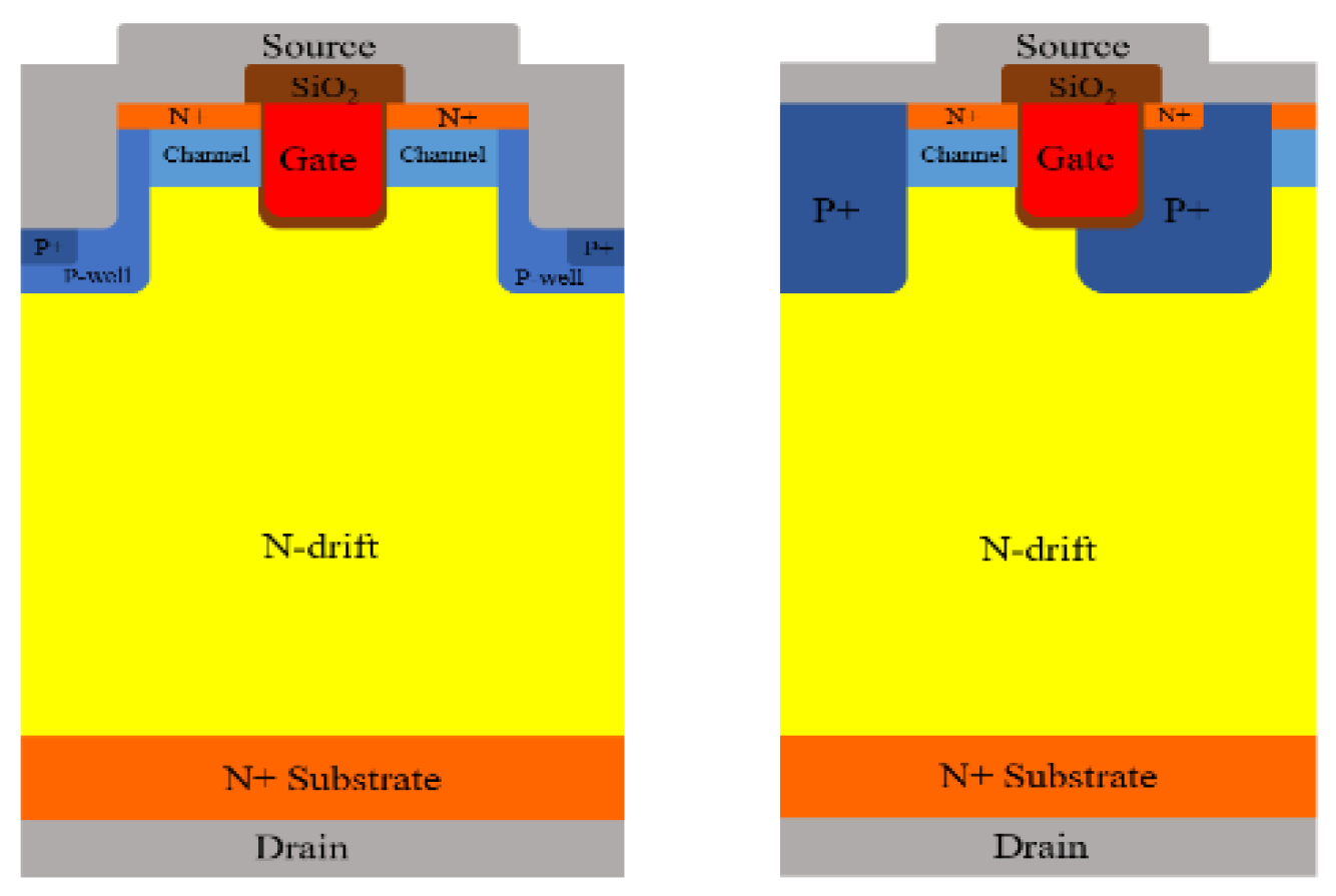
Figure 2.
IS test circuit of 4H-SiC power MOSFET(a) Schematic circuit of UIS test (b) wave form diagram of tested (c) UIS test setup.
Figure 2.
IS test circuit of 4H-SiC power MOSFET(a) Schematic circuit of UIS test (b) wave form diagram of tested (c) UIS test setup.
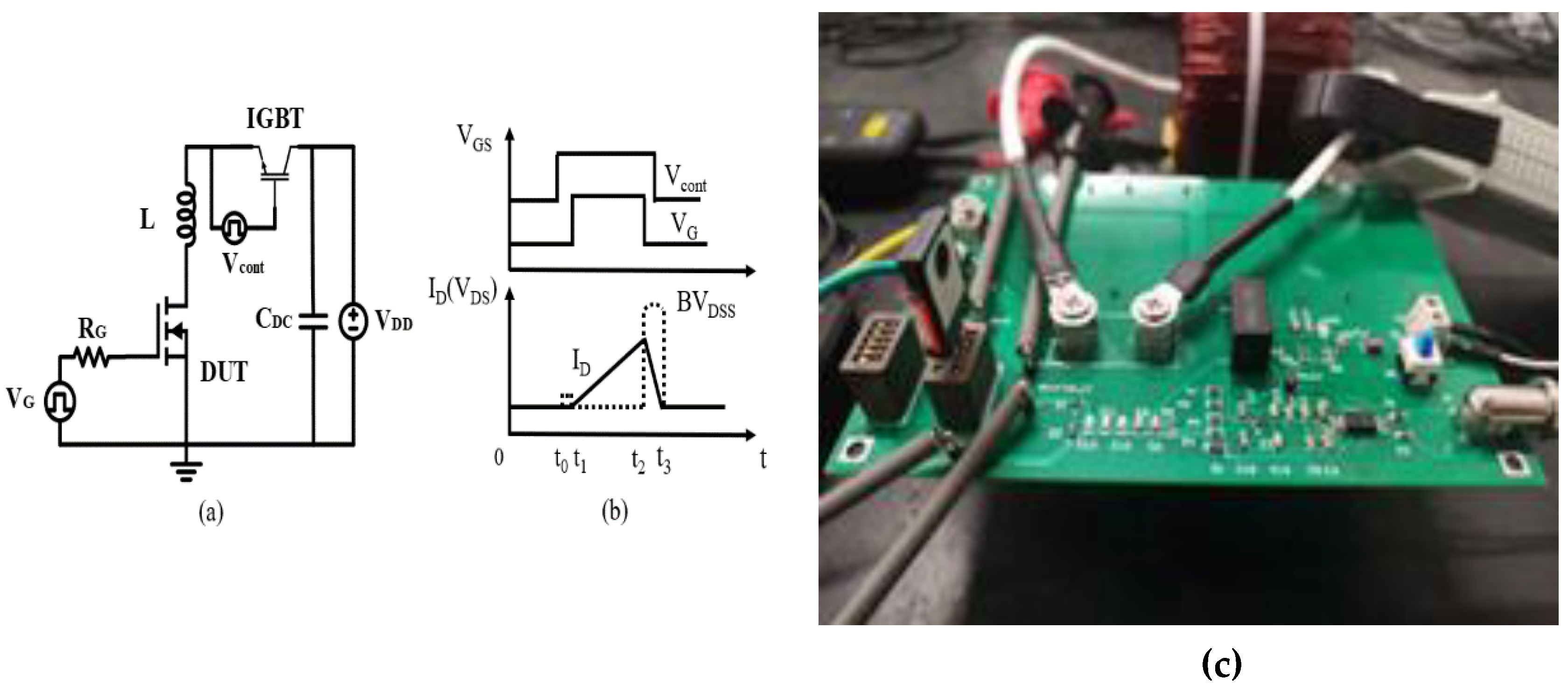
Figure 3.
Single pulse UIS waveforms with load inductor 3mH at the last test before failure(a) DT-MOSFET (b) AT-MOSFET.
Figure 3.
Single pulse UIS waveforms with load inductor 3mH at the last test before failure(a) DT-MOSFET (b) AT-MOSFET.
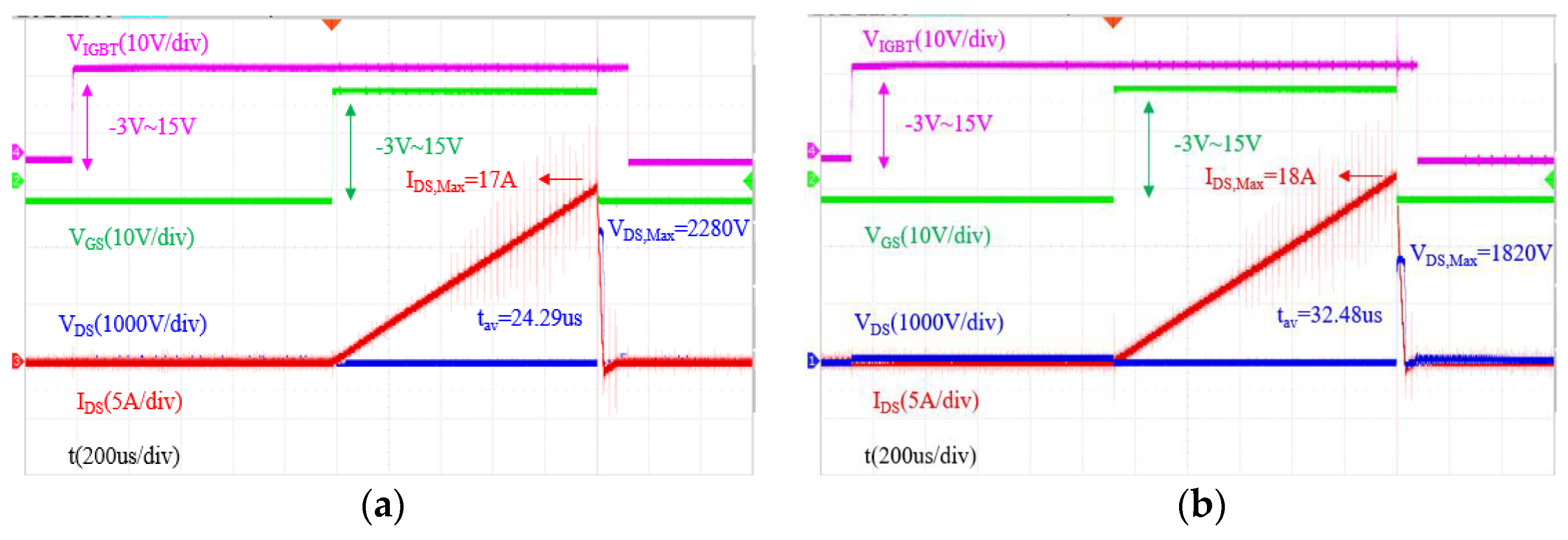
Figure 4.
Single pulse UIS waveforms with load inductor 3mH at failure(a) DT-MOSFET (b) AT-MOSFET.
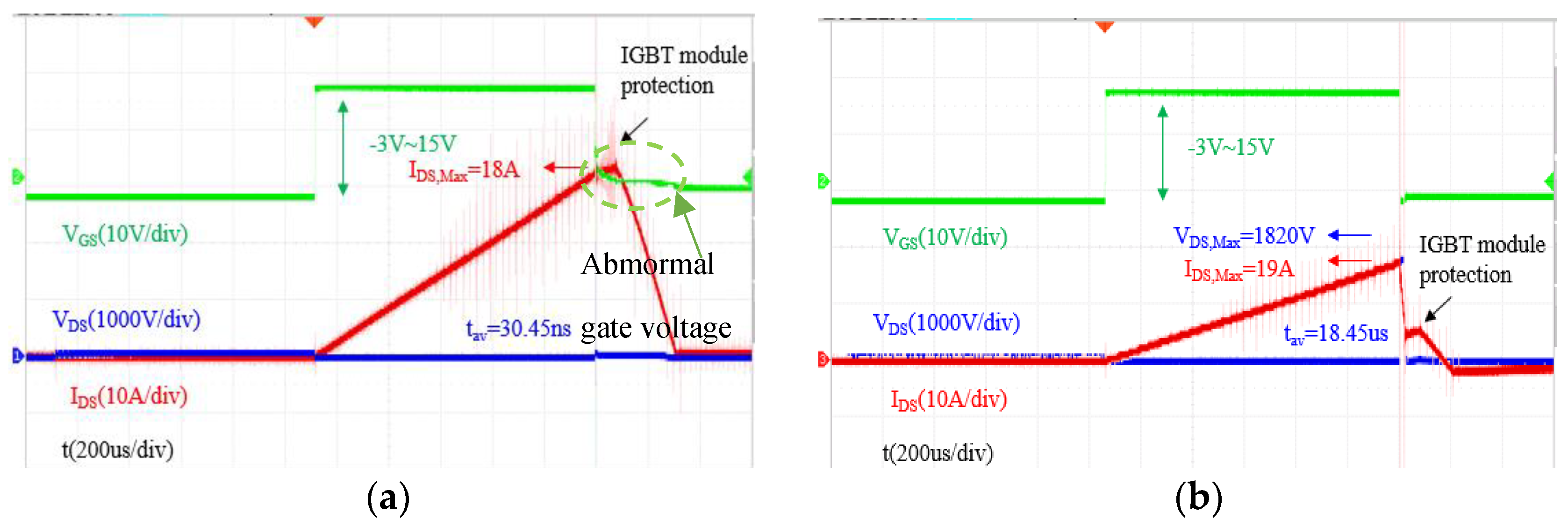
Figure 5.
EAV and tAV versus ton for AT-MOSFET(a) and DT-MOSFET(b) under different ambient temperature with inductor load 3mH.
Figure 5.
EAV and tAV versus ton for AT-MOSFET(a) and DT-MOSFET(b) under different ambient temperature with inductor load 3mH.
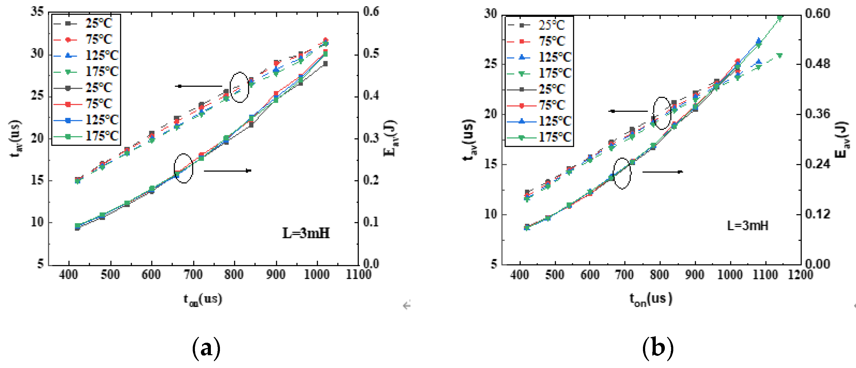
Figure 6.
EAV and tAV versus ambient temperature of AT-MOSFET(a) and DT-MOSFET(b).
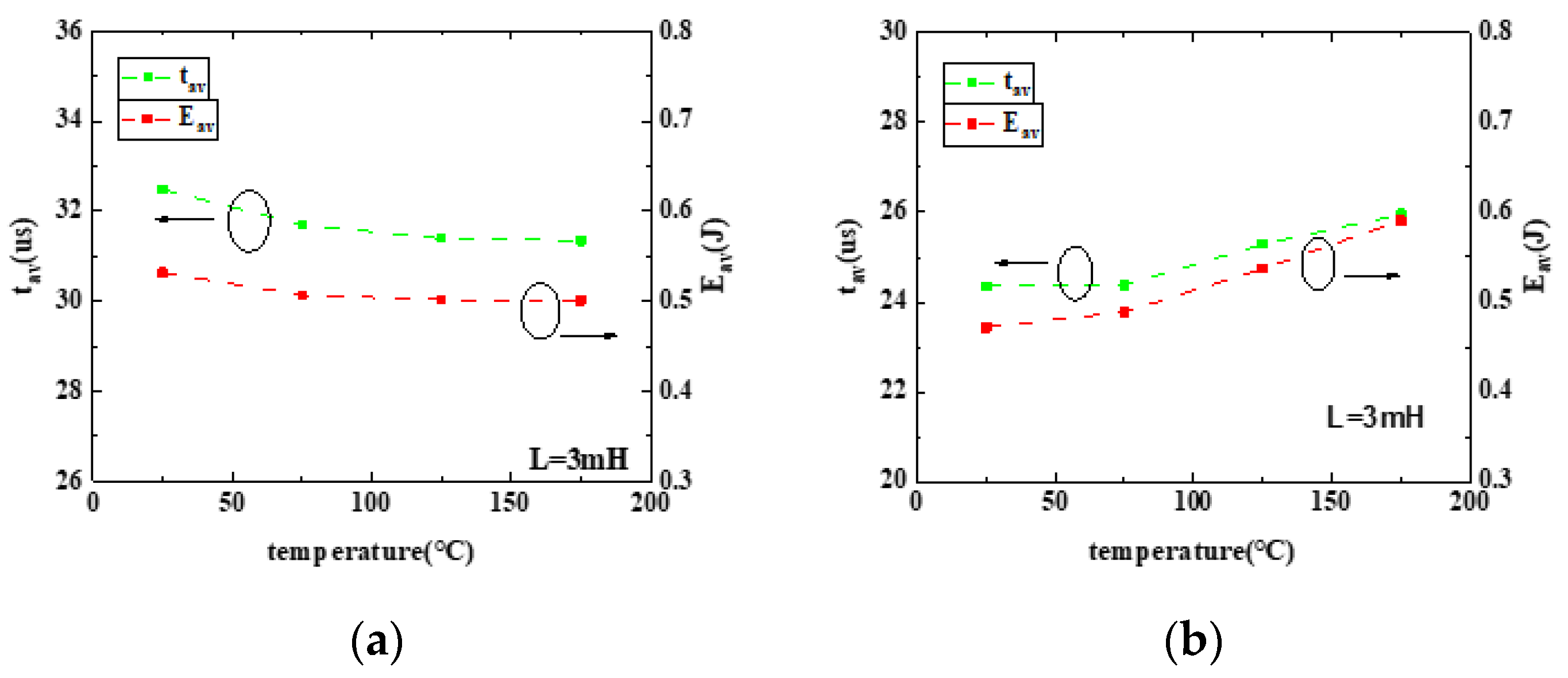
Figure 7.
Ipeak,BVst,Vpeak of DT-MOSFET(b) and AT-MOSFET(a)versus ambient temperature at failure with load inductor 3mH.
Figure 7.
Ipeak,BVst,Vpeak of DT-MOSFET(b) and AT-MOSFET(a)versus ambient temperature at failure with load inductor 3mH.
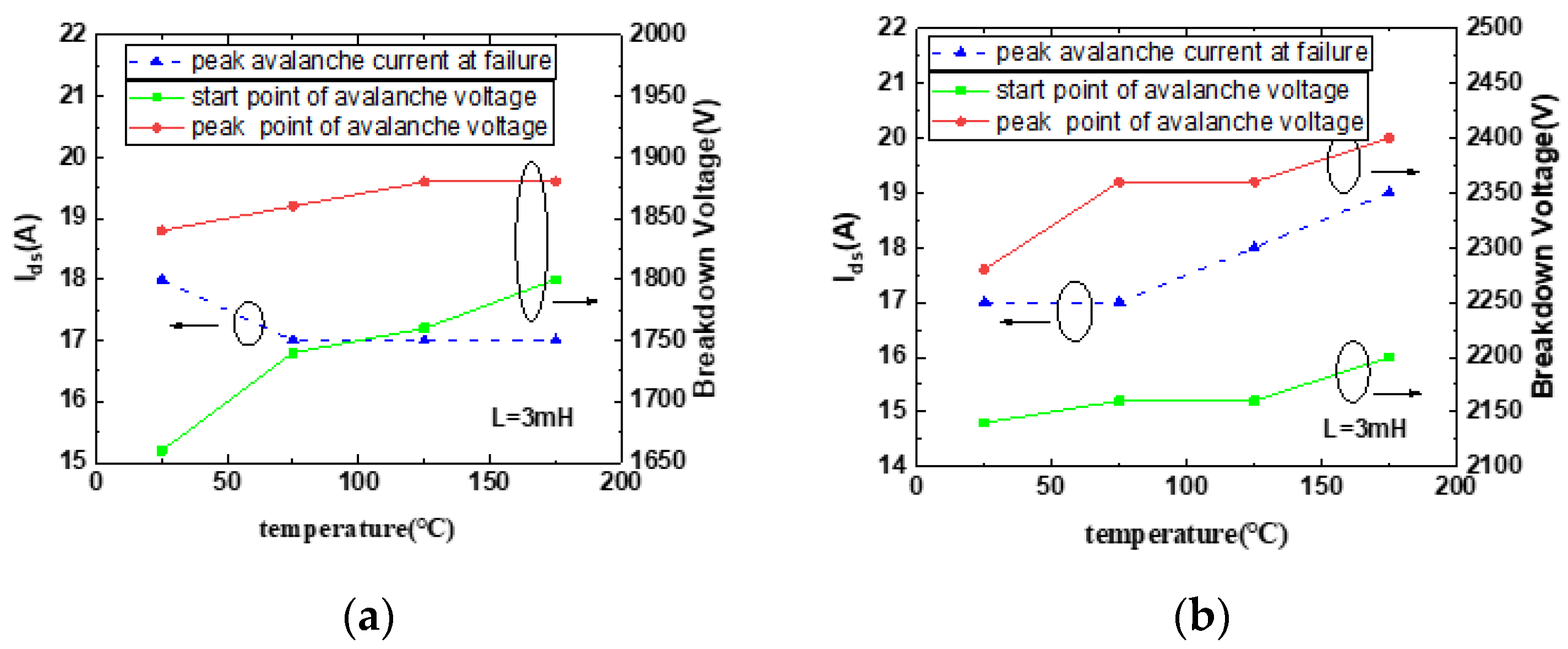
Figure 8.
Decapsulation image of AT-MOSFET (a) and Decapsulation of DT-MOS and failure point at 25℃ (b)and Decapsulation of DT-MOS and failure point at 175℃(c).
Figure 8.
Decapsulation image of AT-MOSFET (a) and Decapsulation of DT-MOS and failure point at 25℃ (b)and Decapsulation of DT-MOS and failure point at 175℃(c).
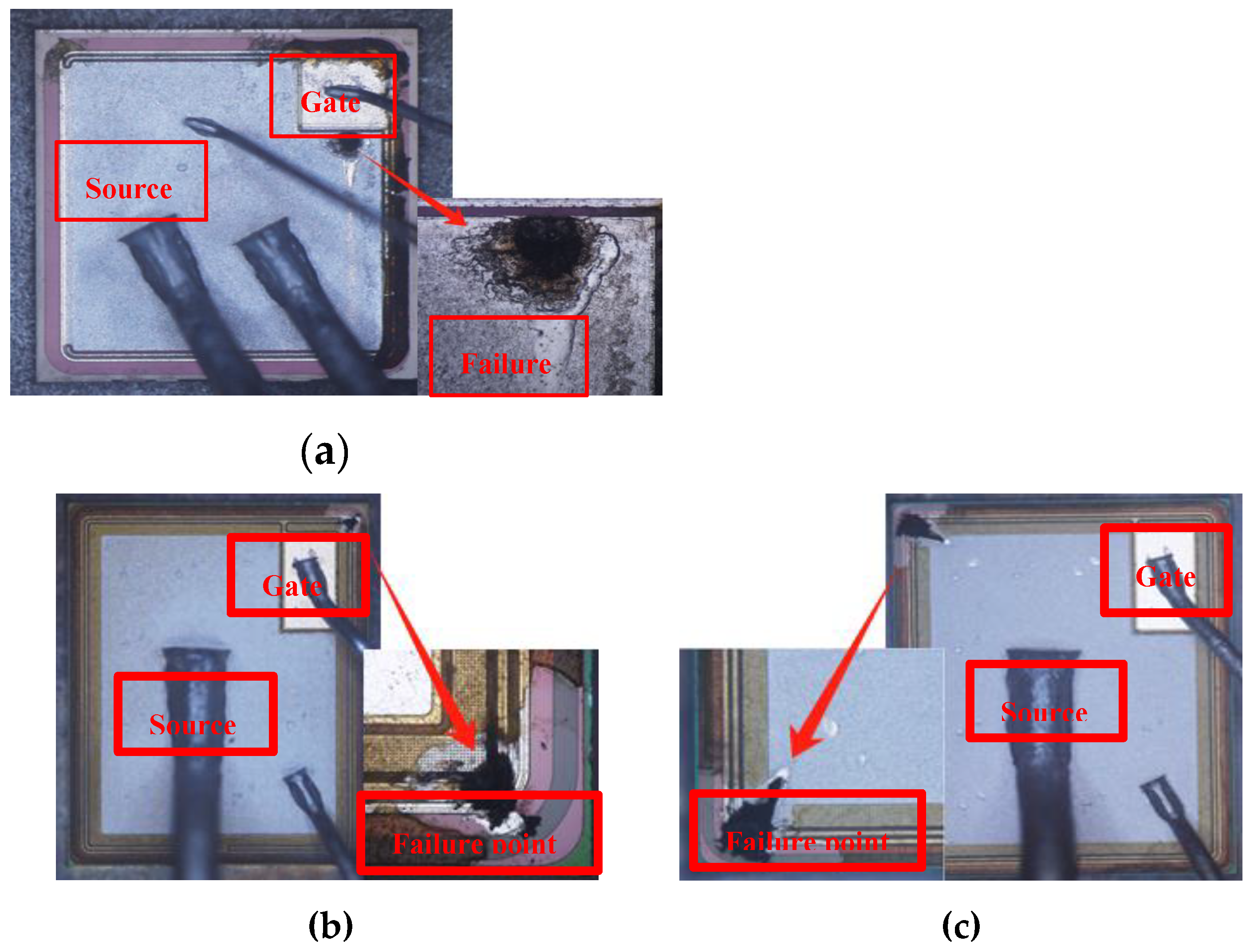
Figure 9.
Repetitive avalanche UIS test waveform diagrams.
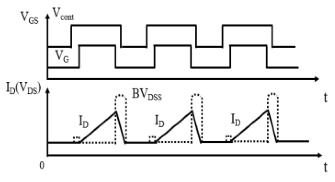
Figure 10.
Vth versus Cycles (a) and Ron versus Cycles (b), Vth and Ron of AT-MOSFET (0.46*0.2=0.09J, L=3mH) and DT-MOSFET (0.19*0.2=0.038J, L=3mH)versus cycles under 20% avalanche energy ratio.
Figure 10.
Vth versus Cycles (a) and Ron versus Cycles (b), Vth and Ron of AT-MOSFET (0.46*0.2=0.09J, L=3mH) and DT-MOSFET (0.19*0.2=0.038J, L=3mH)versus cycles under 20% avalanche energy ratio.
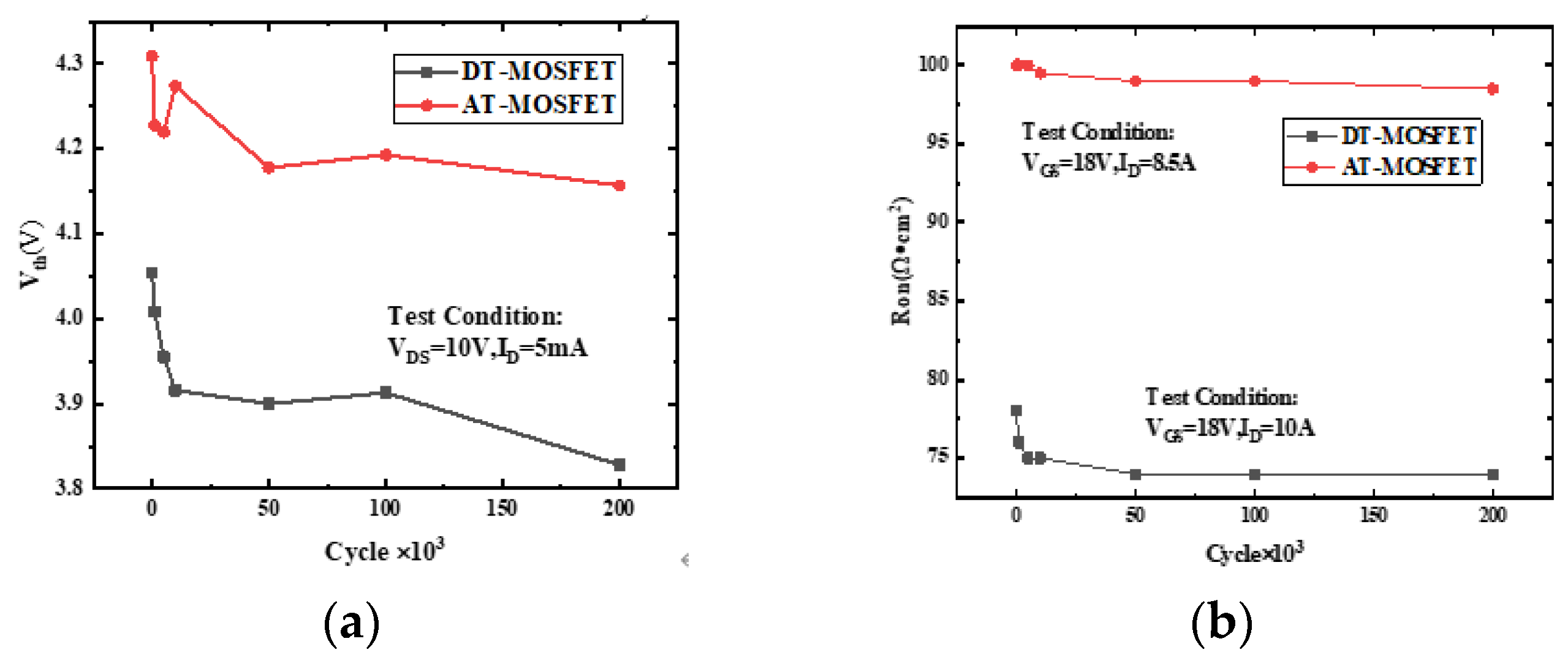
Figure 11.
Igss versus Cycles (a) and Vsd versus Cycles (b), Gate leakage curren(Igss) and forward voltage of body diode(Vsd) of AT-MOSFET and DT-MOSFET under 20% avalanche energy ratio.
Figure 11.
Igss versus Cycles (a) and Vsd versus Cycles (b), Gate leakage curren(Igss) and forward voltage of body diode(Vsd) of AT-MOSFET and DT-MOSFET under 20% avalanche energy ratio.
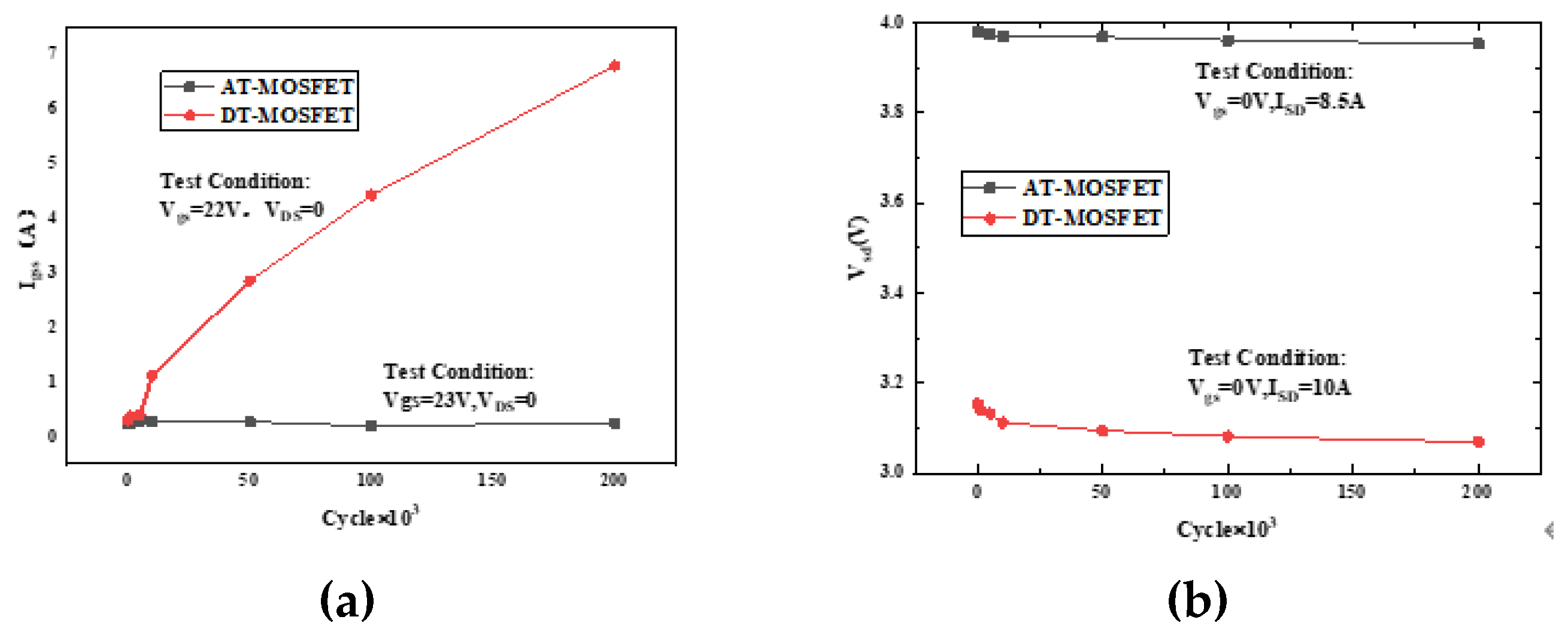
Figure 12.
Electrical field of AT-MOSFET (a) and I.I of AT-MOSFET (b) and Electrical field of DT-MOSFET (c) and I.I of DT-MOSFET (d), Electrical field profile and Impaction Ionization (I.I) of AT-MOSFET and DT-MOSFET under 20% avalanche energy ratio.
Figure 12.
Electrical field of AT-MOSFET (a) and I.I of AT-MOSFET (b) and Electrical field of DT-MOSFET (c) and I.I of DT-MOSFET (d), Electrical field profile and Impaction Ionization (I.I) of AT-MOSFET and DT-MOSFET under 20% avalanche energy ratio.
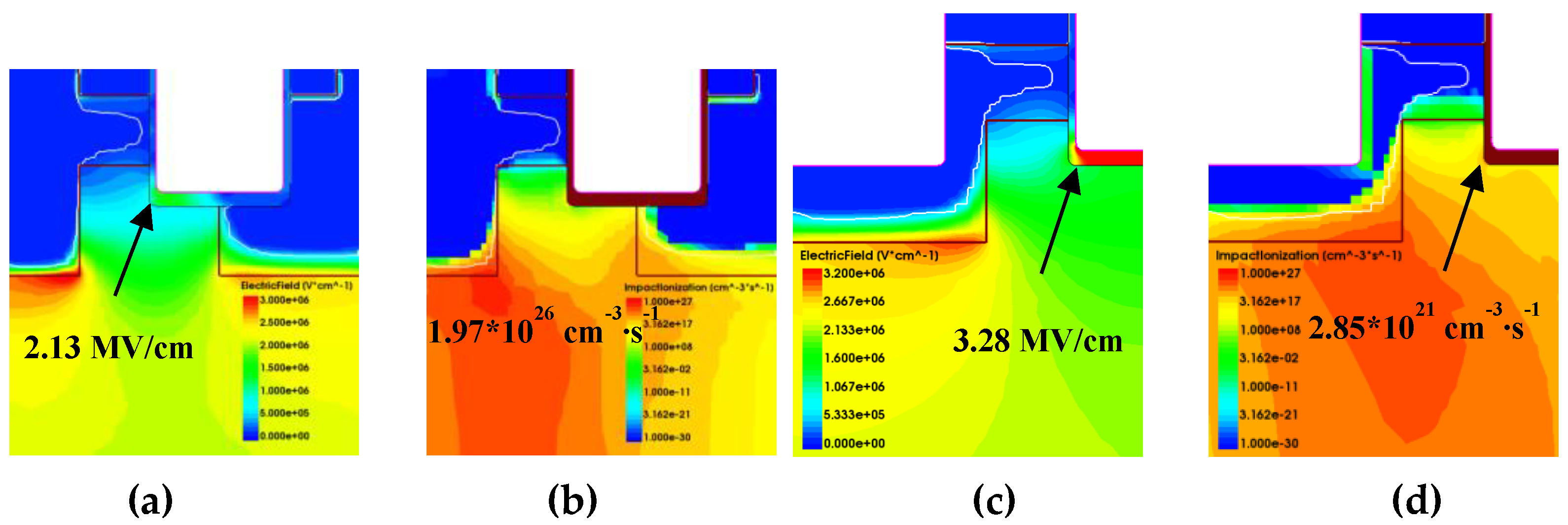
Figure 13.
Cross-section comparation of three devices (a) conventional DT-MOSFET (b) Modified DT-MOSFET (c) Proposed DT-MOSFET.
Figure 13.
Cross-section comparation of three devices (a) conventional DT-MOSFET (b) Modified DT-MOSFET (c) Proposed DT-MOSFET.
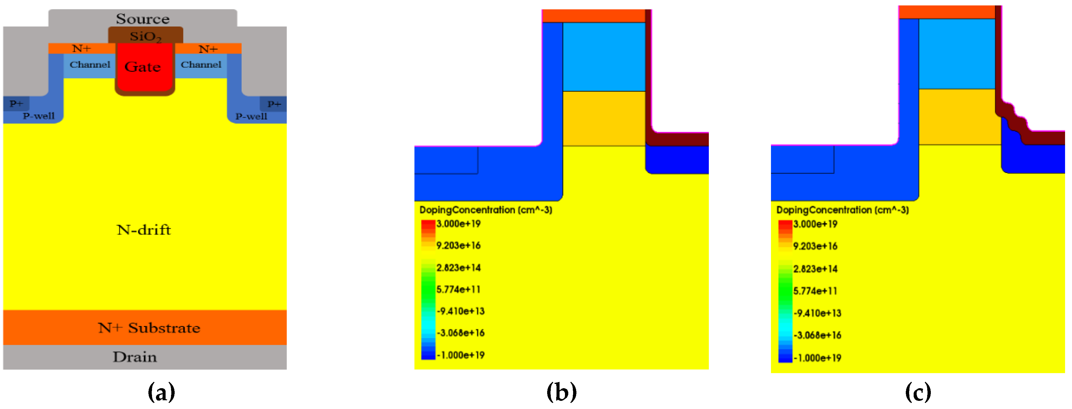
Figure 14.
Electrical field profile in different structrue (avalanche point) (a) conventional DT-MOSFET (b) Modified DT-MOSFET (c) Proposed DT-MOSFET.
Figure 14.
Electrical field profile in different structrue (avalanche point) (a) conventional DT-MOSFET (b) Modified DT-MOSFET (c) Proposed DT-MOSFET.
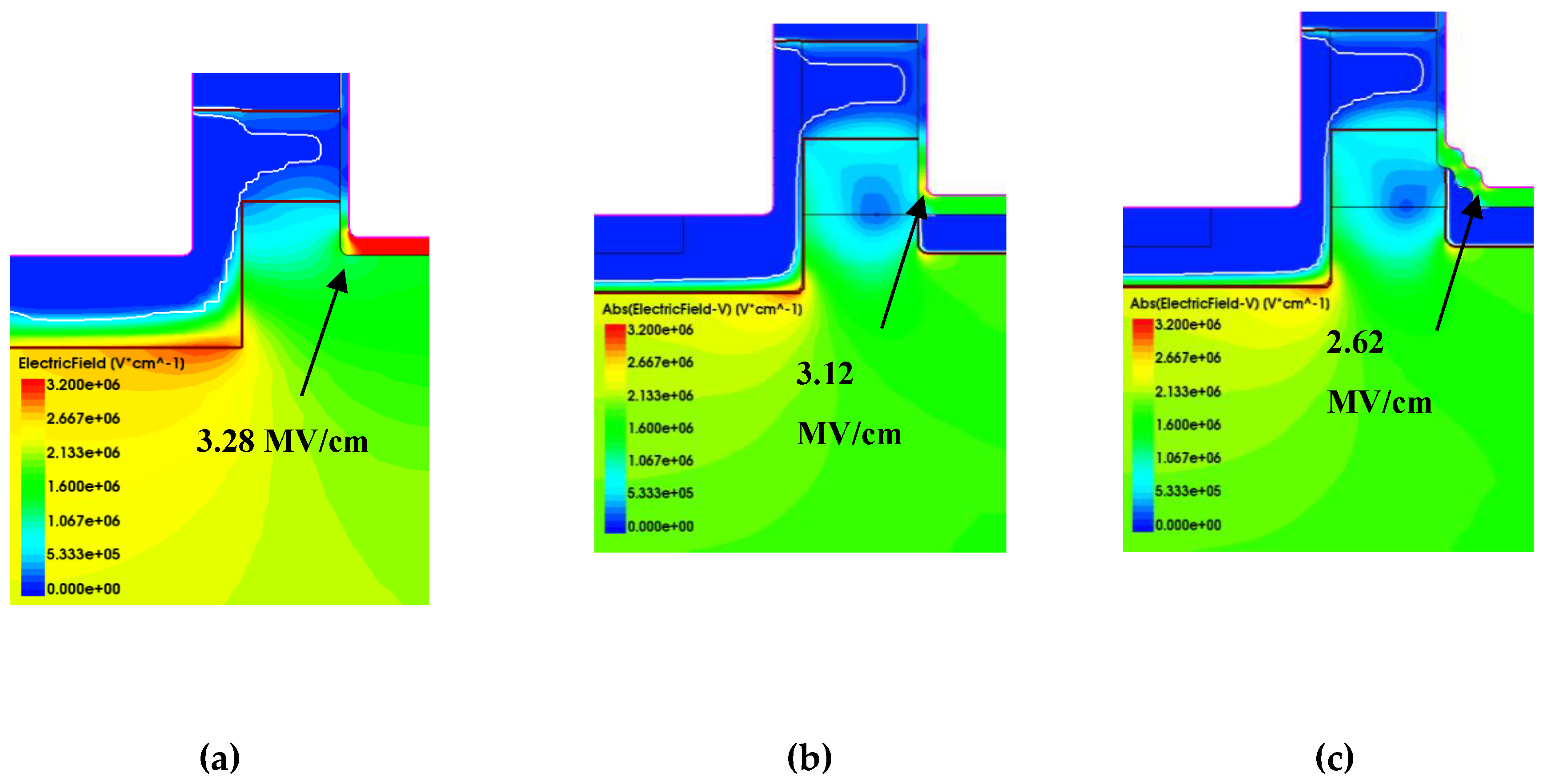
Figure 15.
Blocking characteristics and Ron variation of these three devices.
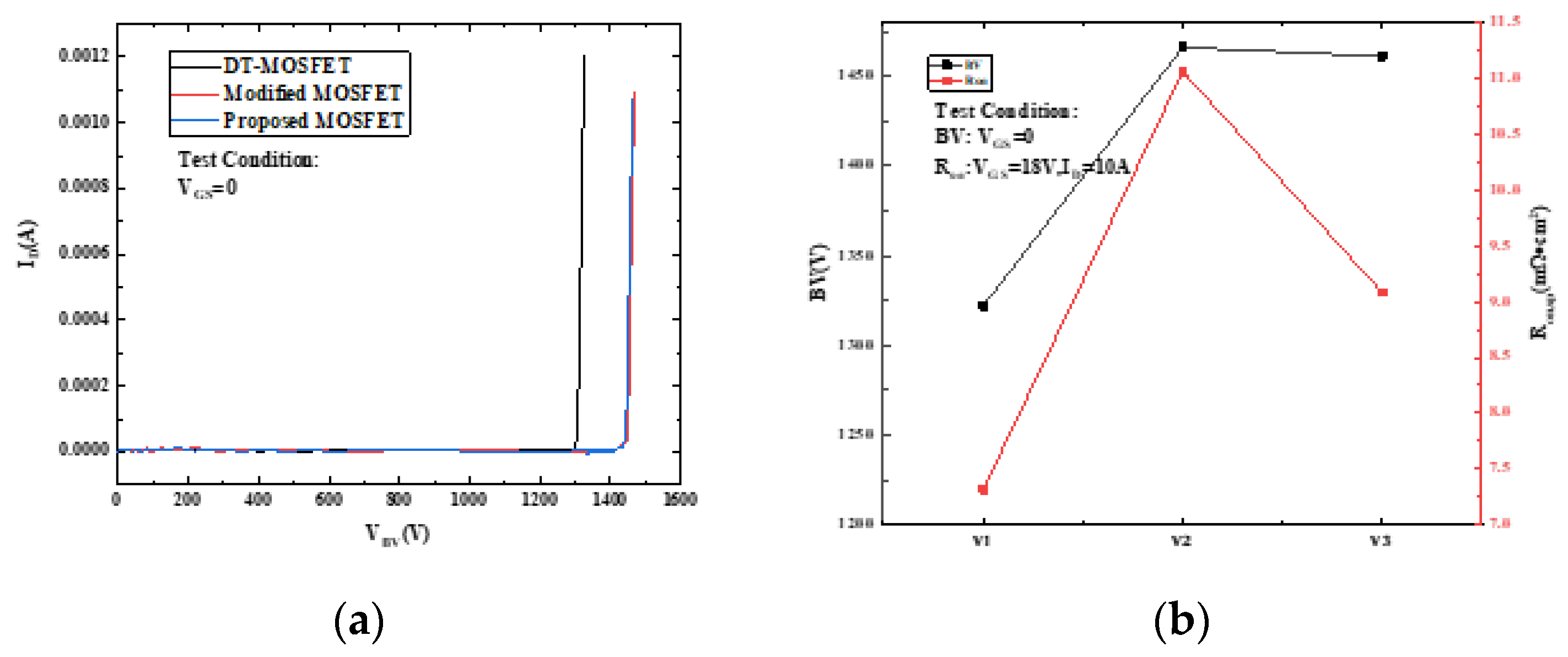

Table 1.
Comparation of EAV, IDS,MAX, VDSMAX and tAV tested under single UIS pulse with different inductor load at room temperature.
Table 1.
Comparation of EAV, IDS,MAX, VDSMAX and tAV tested under single UIS pulse with different inductor load at room temperature.
| Parameters | DT-MOSFET | AT-MOSFET | ||||
| 1mH | 3mH | 10mH | 1mH | 3mH | 10mH | |
| EAV | 0.19J | 0.47J | 0.57J | 0.46J | 0.53J | 0.67J |
| IDS,max | 19A | 18A | 10.5A | 30A | 19A | 11A |
| VDS,Max | 2240V | 2280V | 2320V | 1840V | 1820V | 1800V |
| tAV | 3.13us | 30.45ns | 49.35us | 15.23us | 18.45us | 40 us |
Disclaimer/Publisher’s Note: The statements, opinions and data contained in all publications are solely those of the individual author(s) and contributor(s) and not of MDPI and/or the editor(s). MDPI and/or the editor(s) disclaim responsibility for any injury to people or property resulting from any ideas, methods, instructions or products referred to in the content. |
© 2024 by the authors. Licensee MDPI, Basel, Switzerland. This article is an open access article distributed under the terms and conditions of the Creative Commons Attribution (CC BY) license (http://creativecommons.org/licenses/by/4.0/).
Copyright: This open access article is published under a Creative Commons CC BY 4.0 license, which permit the free download, distribution, and reuse, provided that the author and preprint are cited in any reuse.


