Submitted:
26 April 2024
Posted:
28 April 2024
You are already at the latest version
Abstract
The Yb/Al multilayer films exhibit excellent theoretical reflectivity in the 54-90nm wavelength range. This study attempted to incorporate 1.5% wt.% of Si impurities into Al to suppress the crystallization of Al, reduce interfacial roughness, and enhance the actual reflectivity of the prepared Yb/Al multilayer films. The internal microstructure changes of the film layers before and after Si impurity doping were investigated using GIXRR, AFM, and XRD techniques. The reflectivity of two types of multilayer films, Yb/Al(1.5wt.%Si) and Yb/Al(pure), was tested to evaluate the effect of Si impurity on the film performance.
Keywords:
Yb/Al multilayer
; Si impurity
; 54-90nm wavelength range
1. Introduction
The solar atmosphere in the extreme ultraviolet is used to be observed by the EUV imaging instruments for understanding solar activity [1]. Numerous extreme ultraviolet solar observation satellites have been launched internationally, including the Solar and Heliospheric Observatory (SOHO) [2], the Solar Terrestrial Relations Observatory (STEREO) [3], the Solar Dynamics Observatory (SDO) [4], and the Solar Orbiter [5], which have all advanced relevant research. Multilayer mirrors are the core components of extreme ultraviolet solar observation systems. Above the 115 nm wavelength range, multilayer films with high reflectivity have been fabricated using MgF2 and Al, or MgF2 in combination with other fluorides (such as BaF2, LaF3, and LiF) [6,7,8] . Below the 50 nm range, high reflectivity multilayer films such as Sc/Si [9,10,11] or Mg/SiC [12,13] have been developed. However, within the 54-90 nm range, due to the strong absorption by materials, the fabrication of highly efficient mirrors is challenging. Lanthanide materials exhibit relatively low absorption within the 54-90 nm range, which makes the production of multilayer mirrors feasible within this spectrum. Research by Windt et al. has led to the development of Si/Tb, SiC/Tb, Si/Gd, and Si/Nd multilayer films, which have demonstrated peak reflectance values between 12% and 27% in the 55-69 nm range [14,15,16,17,18].
Among lanthanide materials, ytterbium (Yb) has a lower absorption coefficient in the 55-90 nm range. Yb/Al multilayer films can enhance reflectance in this spectrum. In 2009, Vidal-Dasilva et al. fabricated Yb/Al/Yb/SiO thin films using a thermal evaporation method, achieving peak reflectance values of 27.6% at 80 nm and 24.7% at 85 nm. After two years of storage in a drying cabinet, the peak reflectance at 80 nm decreased to about 20%. The inclusion of a SiO diffusion barrier layer improved the reflectance to 19.1% at 91 nm for Al/SiO/Yb/SiO films, and to 18.3% at 78 nm for Yb/SiO/Al/SiO/Yb/SiO films; this also enhanced storage stability [18]. The addition of a small percentage of silicon (Si) into aluminium (Al) can be an effective method to modify the crystalline structure of the Al layer in multilayer films. Scientists like Zhong and colleagues, by doping Al with around 1% Si, aim to reduce the grain size in the Al layers, which can lead to a smoother interface between the layers [19]. Between 2010 and 2014, Meltchakov et al. improved 39 the deposition process by using Al targets doped with 1.5 wt.% Si or 2 wt.% Cu instead of pure 40 Al. The resulting Al/Mo/B4C multilayers achieved peak reflectivity of 55.5%, 49.8%, and 42.1% at 17.5nm, 20.9nm, and 30.1nm, respectively [20,21,22,23].
In this study, multilayer films of Yb/Al designed to operate at a target wavelength of 73.6 nm were fabricated using pure aluminum and aluminum doped with 1.5 wt.% silicon layers. Employing techniques such as Grazing Incidence X-ray eflectivity (GIXRR), and X−raydiffraction (XRD), Atomic Force Microscopy (AFM), the investigation aimed to analyze the impact of silicon incorporation on the internal structure of the Yb/Al multilayer films. Additionally, extreme ultraviolet (EUV) reflectance measurements were conducted to evaluate the optical performance of the multilayer films.
2. Measurements & Data Analysis
The structural characterization of the sample films was performed via Grazing Incidence X-ray eflectivity (GIXRR) utilizingan X−ray diffractometer (Bede, Durham, United Kingdom) operated in the 2theta-omega configuration. The incident X-ray source was provided by the Cu-Kα radiation at a wavelength of 0.154 nm [24] Reflectivity profiles obtained from GIXRR were subsequently modeled and fitted employing the IMD software to deduce the layer structures and interface quality. Crystalline properties of the multilayers were assessed using X-ray Diffraction (XRD) conducted on a Bruker D8 Advance diffractometer. Diffraction patterns were acquired in symmetric reflection geometry, with the detector scan range set between 25° and 40° at a grazing incidence angle. This arrangement facilitates the detection of crystallographic planes oriented parallel to the surface of the multilayer. Crystallization features were investigated by matching the angular positions of the diffraction peaks to the standard powder diffraction files (PDF) provided by the International Centre for Diffraction Data (ICDD).The mean grain size, oriented perpendicular to the direction of crystal growth, was estimated through the application of the Scherrer equation to broaden diffraction peaks.
where K is a dimensionless shape factor with a value of 0.89 (assuming spherical grains), λ is the X-ray wavelength (0.154 nm for Cu-Kα radiation), B is the full width at half maximum (FWHM) of the XRD peak, and θ is the Bragg angle corresponding to the peak position.
The surface topography of the specimens was meticulously examined utilizing Atomic Force Microscopy (AFM), employing a Bruker Dimension Icon apparatus, which was operated in the tapping mode. The examination entailed scanning areas of disparate dimensions—namely, 10×10 μm², 4×4 μm², and 1×1 μm²—each with a resolution set at 256×256 pixels. To quantify the distribution of surface roughness across various spatial frequencies, the Power Spectral Density (PSD) of the surface was determined using methods derived from Fourier analysis [25].
Reflectivity as a function of angle was measured using a specialized extreme ultraviolet reflectometer [26]. The instrument was equipped with a chopper to facilitate the separation of the reference beam, thus allowing for the precise measurement of very low photocurrents, down to the order of 10 pA. This capability is critical for assessing the angular dependence of reflectivity with high accuracy, especially for samples that demonstrate weak photocurrent signals in the extreme ultraviolet (EUV) region.3. Results.
3. Results & Discussion
3.1. GIXRR
The measured and fitted GIXRR curves of Yb/Al multilayers with two kinds of Al target are shown in Figure 1, where the dotted lines represent the measurements, and the solid line represents the fitting result obtained using the software IMD. The measured curves were fitted with a two- layer model. Table 1 presents the fitted structure of Yb/Al multilayers. Overall, the multilayer structure and performance of the Yb/Al (1.5%wt Si) are significantly better than Yb/Al (pure).
The observation of fewer small reflection peaks in the Grazing Incidence X-Ray Reflectivity (GIXRR) test curves for Yb/Al (pure) multilayer films. When the grazing incidence angle becomes larger than 0.6 degrees, the characteristic peaks of the Yb/Al (pure) multilayer film disappear more quickly due to the factors above, which degrade the X-ray reflectivity performance. This disappearance of peaks at higher angles is less pronounced in the Yb/Al (1.5%wt Si) multilayer films, which maintain their reflectivity characteristics over a broader range of angles, indicative of their superior interface quality. From the fitting results, it can also be observed that the roughness of Yb/Al (1.5%wt Si) is slightly smaller than the roughness of Yb/Al (pure).
3.2. AFM
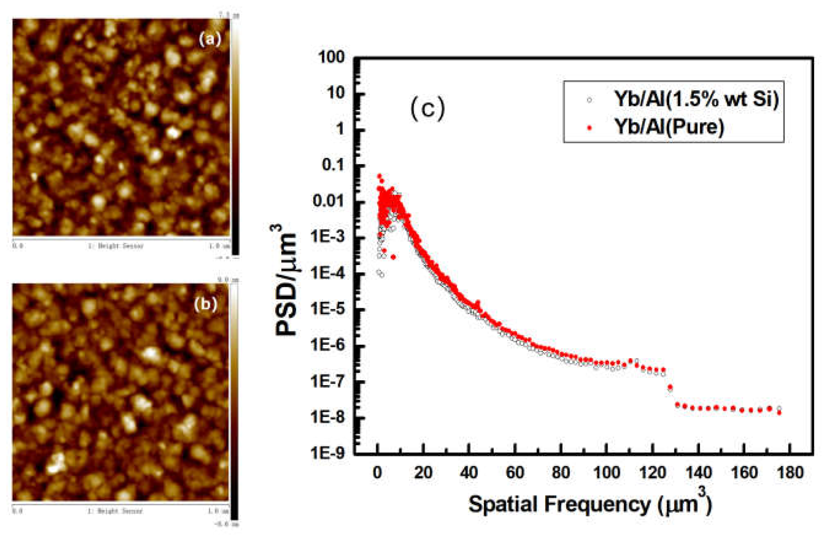
Table 2 delineates the root mean square (RMS) surface roughness of Yb/Al multilayers, ascertained via Atomic Force Microscopy (AFM) across disparate scanning regions. The surface morphology of Yb/Al (pure) multilayers is characterized by the presence of relatively large particulate features, with dimensions approximating 0.1 μm. Such particles contribute to a pronounced surface roughness, an observation that dovetails with the empirical data gathered from Grazing Incidence X-Ray Reflectivity (GIXRR) assessments.

Table 2.
The root mean square (RMS) surface roughness at different test areas of AFM.
| Sample | 10×10 μm² | 4×4 μm² | 1×1 μm² |
|---|---|---|---|
| Yb/Al (pure) | 4.85 nm | 3.01 nm | 2.41 nm |
| Yb/Al (1.5%wt Si) | 1.81 nm | 2.04 nm | 2.09 nm |
Figure 2.
AFM image and the PSD of Yb/Al multilayers: (a) AFM image of Yb/Al (1.5%wt Si), (b) AFM image of Yb/Al (pure), (c) The PSD of the Samples.
Figure 2.
AFM image and the PSD of Yb/Al multilayers: (a) AFM image of Yb/Al (1.5%wt Si), (b) AFM image of Yb/Al (pure), (c) The PSD of the Samples.
3.3. XRD
Figure 3 illustrates the X-ray diffraction (XRD) patterns of Yb/Al multilayer structures recorded in the symmetrical reflection mode. The angular distribution of the diffraction peaks, as observed, manifests at 28.405°, 32.210°, and 38.897°, which may be attributed to the crystallographic planes of Yb (111), Yb2O3 (123), and Al (111), respectively [27,28,29,30]. In the comparative analysis of the diffraction peaks between the Yb/Al (pure) and the Yb/Al (1.5%wt Si) multilayers, a noticeable diminution in the intensity of the peaks for the latter is observed, particularly the peak corresponding to the Al (111) plane, which becomes remarkably subdued. Additionally, the peak associated with Yb (111) exhibits a slight reduction in intensity. Utilizing the Scherrer formula, which relates the FWHM of a diffraction peak to the size of the coherent diffracting domains or crystallites in a polycrystalline sample, the average grain size of the crystallographic phases was quantified. These calculations, presented in Table 3.
Figure 3.
Measured XRD curves of Yb/Al multilayers deposited with different Al layer.
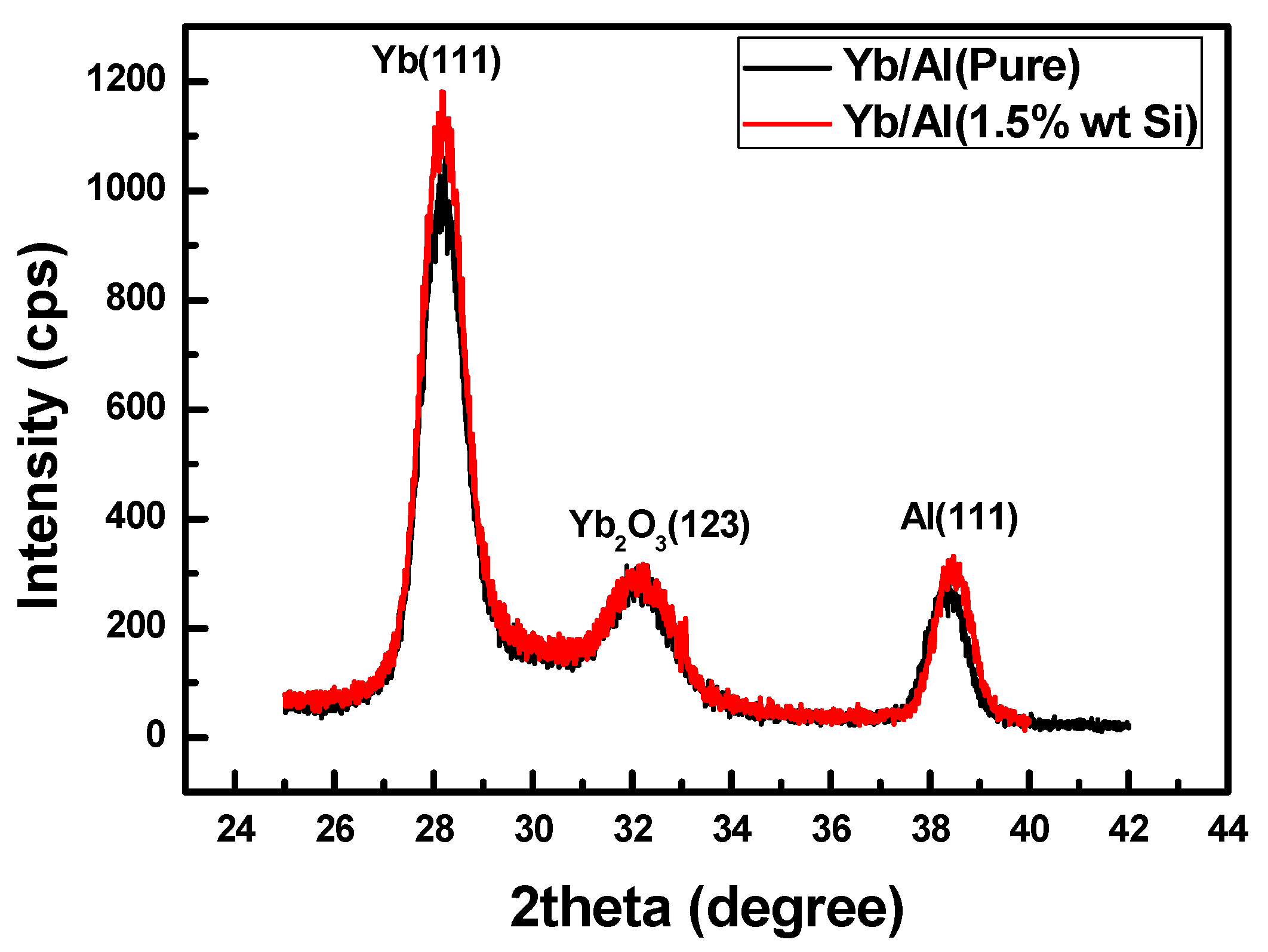
Table 2.
Average grain size of different crystal phases.
| Sample | Yb (111) | Yb2O3 (123) | Al (111) |
|---|---|---|---|
| Yb/Al (pure) | 7.636 nm | 4.865 nm | 8.730 nm |
| Yb/Al (1.5%wt Si) | 7.895 nm | 4.915 nm | 9.318 nm |
The introduction of Si inhibits the crystallization of Al. The relatively weaker crystallization of Al enhances diffusion with Yb, leading to a reduction in the crystallinity of Yb. The diffusion between Al and Yb counteracts the improvement in interfacial roughness resulting from the reduced crystallization of Al. Therefore, the difference in average roughness obtained from GIXRR fitting between Yb/Al (pure)and Yb/Al (1.5%wt Si) is not significant.
3.4. Reflectivity
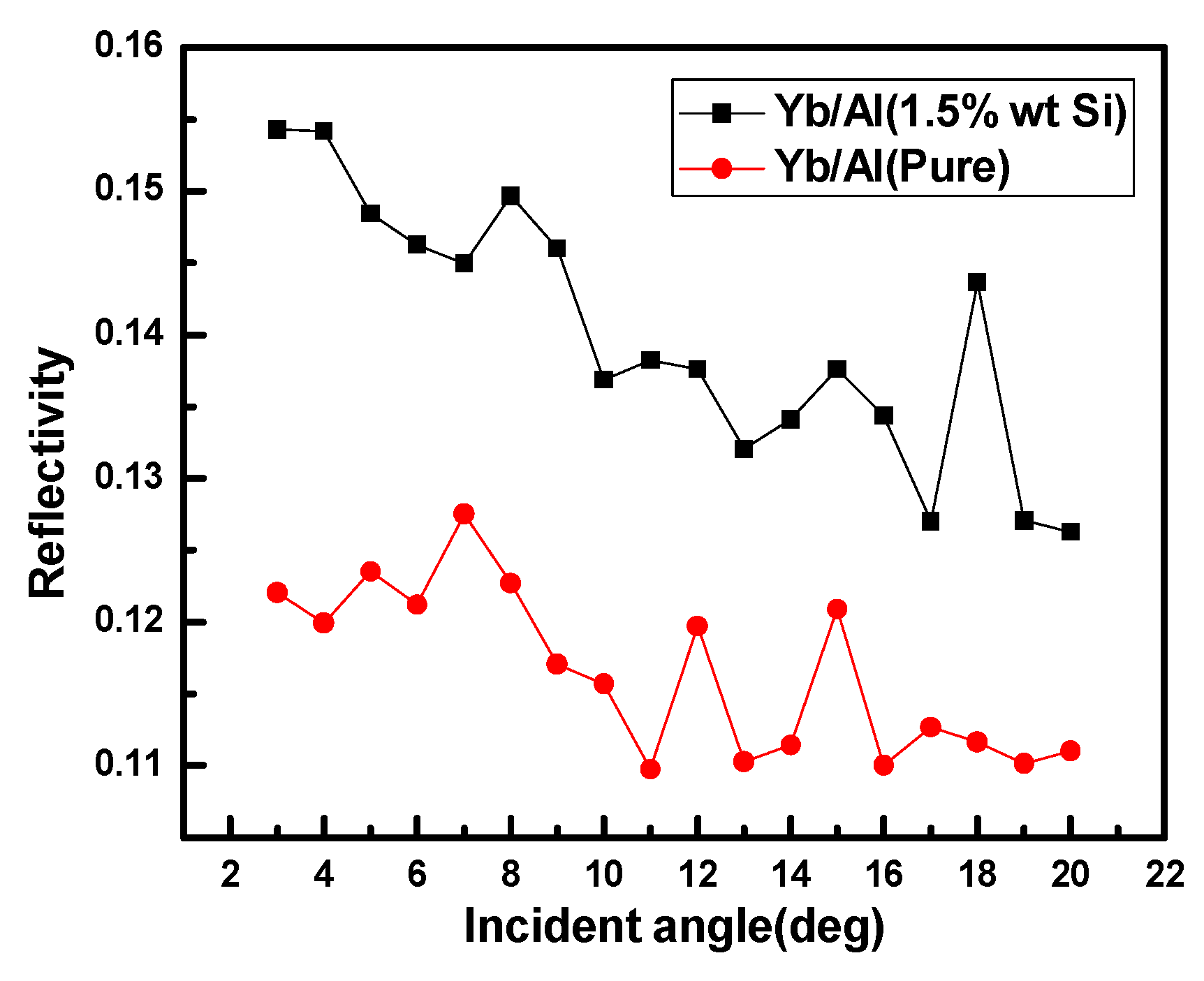
The angular dependency of the reflectivity for the Yb/Al multilayers was systematically investigated and the results are depicted in Figure 5, encompassing a range from 3° to 20° in terms of the incident angle, incremented by 1° intervals. For each specified angle, the detection of the reflected light’s intensity, alongside that of a reference beam, was performed at a sampling rate of 512 Hz. Subsequent to this, a subtraction of the background noise from the signal was executed, ensuring that the data reflects the true reflectivity of the sample. To facilitate comparison, the intensity of the reflected light was normalized against that of the reference beam.
Accompanying the experimental data, Figure 5 provides the theoretical reflectivity curves as computed by the IMD (Integrated Munster Data) software. These curves delineate the expected reflectance of an ideally fabricated multilayer structure with negligible surface roughness. The Yb/Al (pure) and Yb/Al (1.5%wt Si) multilayers exhibit reflectivities of 11.9% and 15.4%, respectively, when subjected to a 4° incidence angle. Notably, the reflectivity of the Yb/Al (1.5%wt Si) surpasses that of the Yb/Al (pure) by approximately four percentage points. However, it is crucial to acknowledge that the obtained values fall short of the theoretical ideal.
This observed discrepancy between the experimental and theoretical reflectivity values is primarily ascribed to a combination of factors including surface roughness, interlayer diffusion, and the onset of oxidation at the surface. Surface roughness can lead to increased scattering of light, thus diminishing the reflectivity. Interlayer diffusion may result in a blurring of the interfaces, which can also adversely affect the reflectance properties. Furthermore, the formation of an oxide layer can alter the electronic structure at the surface, impeding optimal reflection. These phenomena underscore the challenges in the fabrication of multilayer structures where deviations from the ideal design parameters can significantly impact functionality. We attribute this discrepancy to roughness, interlayer diffusion and surface oxidation.
Figure 4.
Reflectivity curve with changing incident angle from 3 deg to 20 deg.
4. Conclusion
In a direct current (DC) magnetron sputtering system, two types of Yb/Al multilayer films were fabricated using pure Al targets and Si-doped Al targets. A suite of characterization techniques, including Grazing Incidence X-Ray Reflectometry (GIXRR), Atomic Force Microscopy (AFM), X-Ray Diffraction (XRD),and angular dependence of reflectivity studies, revealed significant differences in the structure and performance between the two multilayer materials.
The Yb/Al (1.5 wt% Si) multilayer films demonstrated superior reflective performance. X-Ray Diffraction analysis indicated that the incorporation of Si effectively reduced the grain size within the Al layers and slightly decreased the crystallinity of Yb. These combined effects led to a decrease in interfacial roughness, which positively impacted the reflectivity and the outcomes of the rocking curve analysis. Notably, the reduction in interfacial roughness played a critical role in enhancing specular reflection and reducing non-specular scattering.
Furthermore, Power Spectral Density (PSD) analysis corroborated the improvement in surface and interfacial quality due to Si doping, as reflected in the lower surface roughness and more optimized interlayer transitions.
In summary, the introduction of Si, by finely tuning the structural properties of the multilayer films, not only enhanced the specular reflectivity of Yb/Al multilayer films but also reduced non-specular scattering. This led to a significant improvement in performance for optical applications such as high-precision mirrors and optical coatings. These findings underscore the importance of material engineering in the design of multilayer films, particularly with respect to the quality of optical interfaces in high-performance optical applications.
Author Contributions
Conceptualization, experiment, formal analysis, and writing—original draft, B.L.; XRR testing and analysis, Z.Z.; funding acquisition, supervision, and project administration, R.Q.; reviewing, and editing, Z.W. All authors have read and agreed to the published version of the manuscript.
Funding
This research was funded by the National Key R&D Program of China (Grant no. 2023YFA1608803).
Institutional Review Board Statement
Not applicable.
Informed Consent Statement
Not applicable.
Data Availability Statement
The data presented in this study are available on request from the corresponding author.
Conflicts of Interest
The authors declare no conflict of interest.
References
- Corso.; Pelizzo. Extreme ultraviolet multilayers for solar physics, 2nd ed.; 2019.
- Domingo, V.; Fleck, B.; Polandai. The solar and heliosphereic observatory. Space Science Reviews; SOHO, 1995; 72(1-2), 81-84. [CrossRef]
- Kaiser. M.L.; Kucera. T.; Davila. J.M. The stereo mission: An introduction. Space Science Reviews 2008, 136, 5–16. [CrossRef]
- Pesnell. W.D.; Thompson. B.J.; Chamberlin. P.C. The solar dynamics observatory (SDO), Springer.; New York, 2011; 3-15. [CrossRef]
- Marsch. E.; Marsden. R.; Harrison. R. Solar Orbiter-mission profile, main goal sand present status. Advances in Space Research 2005, 36, 1360–1366.
- Zuki. C.M.; Torr. D.G. Multiple reflectors as narrow-band and broad band vacuum ultraviolet filters. Applied Optics 1992, 31, 1588–1596.
- Zuki. C.M.; Torr. D.G.; Kim. J. Filters for the international solar terrestrial physics mission far-ultraviolet imager. Optical Engineering 1993, 32, 3069–3074.
- Gatto. A.; Thielsch. R.; Heber. J.; Kaiser. N.; Ristau. D.; Günster. S.; Kohlhaas. J.; Marsi. M.; Trovò. M.; Walker. R.; Garzella. D.; Couprie. M.E.; Torchio. P.; Alvisi. M.; Amra. C. High-performance deep-ultraviolet optics for free-electron lasers. Applied Optics 2002, 41, 3236–3241. [CrossRef]
- Uspenskii. Y.A.; Levashov. V.E.; Vinogradov. A.V.; Fedorenko. A.I.; Kondratenko. V.V.; Pershin. Y.P.; Zubarev. E.N.; Fedotov. V.Y. High-reflectivity multilayer mirrors for a vacuum ultraviolet interval of 35–50nm.Optics Letters 1998, 23, 771–773. [CrossRef]
- Yu. L.S.; Schaefer. S.F.; Feigl. T. Enhanced reflectivity and stability of Sc/Si multilayers, 2004. SPIE5193:155-163.
- Gautier. J.; Delmotte. F.; Bridou. F. Characterization and optimization of magnetron sputtered Sc/Si Multilayers for Extreme Ultraviolet Optics. Applied Physics A 2007, 88, 719–725. [CrossRef]
- Takenaka. H.; Ichimaru. S.; Ohchi. T. Soft-X-ray reflectivity and heat resistance of SiC/Mg multilayer. Journal of Electron spectroscopy and Related Phenomena 2005, 144, 1047–1049. [CrossRef]
- Martínez. G.; Boernerp.; Souflir. The high-resolution lightweight telescope for the EUV(HiLiTE), 2008. SPIE7011:70113K.
- Windt. D.L.; Seely. J.F.; Kjornrattanawanich. B.; Uspenskii. Y.A. Terbium-based extreme ultraviolet multilayers. Optics Letters 2005, 30, 3186–3188. [CrossRef]
- Kjornrattanawanich. B.; Windt. D.L.; Seely. J.F.; Uspenskii. Y.A. SiC/Tb and Si/Tb multilayer coatings for extreme ultraviolet solar imaging. Applied Optics 2006, 45, 1765–1772. [CrossRef]
- Kjornrattanawanich. B.; Windt. D.L.; Seely. J F. Normal-incidence silicon–gadolinium multilayers for imaging at 63nm wavelength. Optics Letters 2008, 33, 965–967. [CrossRef]
- Kjornrattanawanich. B.; Windt. D.L.; Uspenskii. Y.A. Optical constants determination of neodymium and gadolinium in the 3-to100-nm wavelength range, 2006. SPIE6317:63170U.
- Vidal. D.M.; Fernández. P.M.; Méndezja. Narrow band multilayer coatings for the extreme ultraviolet range of 50-92nm. Optics Express 2009, 17, 22773–22784.
- Zhong. Q.; Zhang. Z.; Ma. S.; Qi. R.Z.; Wu. J.L.; Wang. Z.S.; Jonnard. P.; Guen. L.; André. J.M. The transition from amorphous to crystalline in Al/Zr multilayers, 2012.
- Meltchakov. E. Development of Al-based multilayer optics for EUV. PHYS.; Mater: APPL, 2010; 98, 111–117. [CrossRef]
- Meltchakov. E. EUV reflectivity and stability of tri-component Al-based multilayers. SPIE, 2011; 8168.
- Meltchakov. E. Single and multi-channel Al-based multilayer systems for space applications in EUV range. SPIE 2013; 8777.
- Delmotte. Development of multilayer coatings for solar orbiter EUV imaging telescopes, 2013. SPIE:177 8862.
- Wormington. M.; Panaccione. C.; Matney. K.M.; Bowen. D.K. Characterization of structures from X-ray scattering data using genetic algorithms, Philosophical Transactions of the Royal Society of London. Series A: Mathematical. Physical and Engineering Sciences 1999, 357, 2827–2848. [CrossRef]
- Feng. J.; Huang. Q.; Wang. H.; Yang. X.; Giglia. A.; Xie. C.; Wang. Z. Structure, stress and optical properties of Cr/C multilayers for the tender X-ray range. J Synchrotron Rad 2019, 26, 720–728.
- Yu. Y.; Ye. Z.; J. L.; Yao. Q. Laboratory-based reflectometer using line spectra of an RF-induced gas-discharge lamp in 30- to 200-nm wavelength range. Journal of Astronomical Telescopes, Instruments, and Systems 2022, 8, 017002.
- Peymani. M.S.M.; Sobhani. N.A.; Rostami. M. Assessing the magnetic, cytotoxic and photocatalytic influence of incorporating Yb3+ or Pr3+ ions in cobalt–nickel ferrite. Journal of Materials Science: Materials in Electronics 2019, 30, 6902–6909.
- Permin. D.A.; Novikova. A.V.; Koshkin. V.A. Fabrication and Magneto-Optical Properties of Yb2O3 Based Ceramics. Magnetochemistry 2020, 6, 63.
- Kahraman. A.; Karacali. H.; Yilmaz. E. Impact and origin of the oxide-interface traps in Al/Yb2O3/n-Si/Al on the electrical characteristics. Journal of Alloys and Compounds 2020, 825, 154171.
- Hao. L.; He. G.; Fang. Z. Modulation of the microstructure, optical and electrical properties of sputtering-driven Yb2O3 gate dielectrics by sputtering power and annealing treatment. Applied Surface Science 2020, 508,145273.
Figure 1.
Measured and fitted GIXRR curves of Yb/Al multilayers deposited with different Al layer.
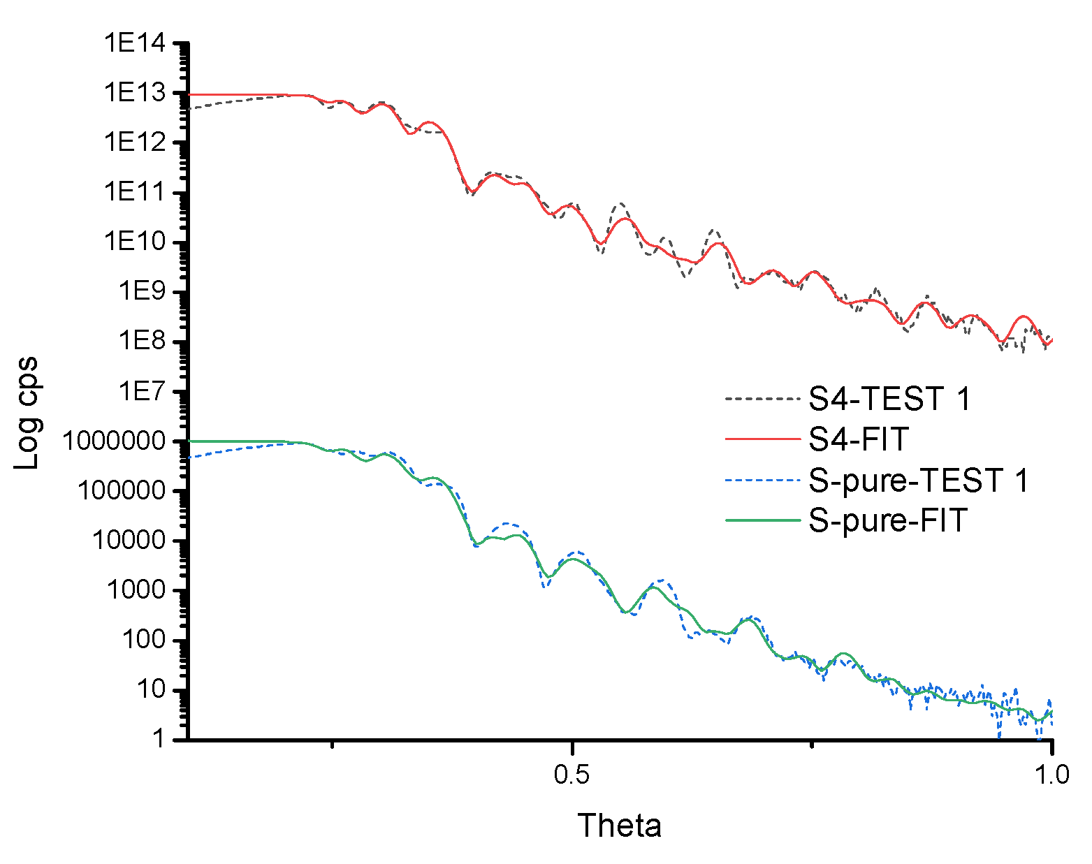
Table 1.
GIXRR fitting results of Yb/Al multilayers deposited with different Al layer.
| Sample | SiC thickness | Yb thickness | Al thickness | Averge roughness |
|---|---|---|---|---|
| Yb/Al (pure) | 9.87 nm | 19.28 nm | 41.44 nm | 1.95 nm |
| Yb/Al (1.5%wt Si) | 9.68 nm | 20.57 nm | 38.78 nm | 1.89 nm |
Disclaimer/Publisher’s Note: The statements, opinions and data contained in all publications are solely those of the individual author(s) and contributor(s) and not of MDPI and/or the editor(s). MDPI and/or the editor(s) disclaim responsibility for any injury to people or property resulting from any ideas, methods, instructions or products referred to in the content. |
© 2024 by the authors. Licensee MDPI, Basel, Switzerland. This article is an open access article distributed under the terms and conditions of the Creative Commons Attribution (CC BY) license (http://creativecommons.org/licenses/by/4.0/).
Copyright: This open access article is published under a Creative Commons CC BY 4.0 license, which permit the free download, distribution, and reuse, provided that the author and preprint are cited in any reuse.


