Submitted:
03 April 2024
Posted:
04 April 2024
Read the latest preprint version here
Abstract
In this paper, the single event burnout(SEB) and reinforcement structure of 1200V SiC MOSFET (SG-SBD-MOSFET) with split gate and schottky barrier diode(SBD) embedded were studied. The device structure was established using Sentaurus TCAD, and the transient current changes of single event effect(SEE), SEB threshold voltage, as well as the regularity of electricfield peak distribution transfer were studied when heavy ions were incident from different regions of the device. Based on SEE analysis of new structural device, two reinforcement structure designs for SEB resistance were studied, namely the expansion of P+body contact area and the design of multi-layer N-type interval buffer layer. Firstly, two reinforcement schemes for SEB were analyzed separately, and then comprehensive design and analysis were carried out. The results showed that the SEB threshold voltage of heavy ions incident from the N+source region was increased by 16% when using the P+body contact area extension alone; When the device is reinforced with multi-layer N-type interval buffer layer alone, the SEB threshold voltage increases by 29%; The comprehensive use of P+body contact area expansion and multi-layer N-type interval buffer layer reinforcement increased the SEB threshold voltage by 33%. Overall, the breakdown voltage of the reinforced device decreased from 1632.935V to 1403.135V, which can be seen as reducing the remaining redundant voltage to 19%. The device performance was not significantly affected.
Keywords:
power device
; SiC MOSFET
; split gate
; SBD-embedded
; single event effect
; irradiation hardening
1. Introduction
With the development of SiC technology, SiC MOSFET have become one of the fastest growing power devices. In power electronic systems, power MOSFET play an important role in motor driven inverters and DC-DC conversion circuits. In converter circuits, a diode is usually used in reverse parallel as a freewheeling diode for freewheeling, which can cause problems such as volume increase and parasitic effect, thereby limiting switching frequency and reducing power density. In theory, freewheeling diodes can directly use the parasitic PIN diodes inside SiC MOSFET. However, on the one hand, prolonged switching between the first and third quadrants of SiC MOSFET can cause bipolar degradation effect and reduce device reliability. On the other hand, the conduction voltage in the third quadrant of the body diode is higher and the conduction loss is greater. In order to solve the above problems, many studies have integrated SBD with lower conduction voltage into SiC MOSFET as third quadrant freewheeling diode [1,2,3,4,5,6].
When SiC MOSFET are used as converters in spacecraft power systems, this hind of SiC MOSFET with SBD embedded is also a direction that can be attempted. Therefore, the research object in this paper is SG-SBD-MOSFET.
2. Analysis of Single Event Effect
2.1. Device Structure
The structure of the 1200V SiC MOSFET device with split gate and SBD embedded studied in this article is shown in Figure 1. The relevant parameters are as follows, the doping concentration and thickness of the N-drift are 5.0×1015cm−3 and 10μm, respectively. The doping concentration of substrate is 1.0×1019cm−3, and Wjfet representing the width of the JFET region is 3μm. X representing the width of the half cell grid covering the JFET region is 0.5μm.
2.2. Principle of Single Event EFFECT
The process of SEE is as follows,in a blocked state, a large number of electron- hole pairs are generated by impact ionization after heavy ions are incident into SiC MOSFET. Under the electricfield formed by the bias voltage of the drain-source, electrons move towards the drain electrode, holes move towards the source electrode, enter the P-well, and then move to the P+body contact region,which changes the electricfield distribution in the N-drift, and a high electricfield peak appears at the homojunction formed by N-drift and substrate. Under the action of the high electricfield, intense impact ionization occurs after acceleration, further producing extremely high concentrations of electron-hole pairs. When the carrier avalanche doubling effect occurs, it causes a transient large current. The source and drain electrodes form a conductive path.
SEB is mainly affected by electricfield. The electricfield provides energy for the impact ionization process between electron-hole and silicon carbide atoms. The electron-hole pairs accelerate the impact ionization process by obtaining kinetic energy through the energy provided by the electricfield. The relative velocity of generation and recombination of electron-hole pairs is affected by the magnitude of the electricfield. When the electricfield is weak and the generation speed of electron- hole pairs is smaller than the recombination speed, the magnitude of the single event transient current will gradually decrease to zero over time; In the case of a strong electricfield, the generation speed of electron-hole pairs is greater than the recombination speed, the transient current remains at a stable level over time,SEB effect occurs, and when the bias voltage applied to the device causes the SEB effect to occur, the critical voltage is defined as the SEB threshold voltage, at which the device that experiences SEB will permanently fail.
2.3. Analysis of Single Event Burnout Effect at Different Incident Positions
The sensitivity of different positions of the device to incident particles varies. Figure 2 shows three SEE incident positions selected from three different regions of the device, namely position A above the midpoint of the JFET region, position B above the edge of the split gate, and position C above the PN junction formed by the N+source and P-well in the source region.
Figure 3 shows the transient current curves at different incident positions in different regions. According to the experimental and the irradiation requirements in the actual space environment, the LET is not less than 75MeV·cm2/mg, the unit of energy is represented by pC/μm in the simulation, and the conversion formula for LET is 1pC/μm=151MeV/mg/cm2, therefore, the LET is generally greater than 0.5pC/μm [7,8]. During the simulation research, the bias condition are as follows, LET=0.5pC/μm,VGS=0V, VDS=400V.
From Figure 3, it can be seen that the transient current variation trend is consistent at different incident positions. After heavy ions are incident into the device from different positions, the current increases sharply with time, reaching a transient peak current at around 10ps. Due to the bias voltage does not reach the SEB threshold voltage of the device, the transient current will recover to 0 after a certain period of time. Among them, position B has the greatest variation and is most sensitive to the SEB effect, and the transient current changes most dramatically with time.
Figure 4 shows the transient current curves over time at different bias voltages when incident from position B, which is the most sensitive to SEE. From Figure 4, it can be seen that when the bias voltage reaches 430V, the drain current reaches its peak at 10ps and then remains at a stable value, does not return to the initial state after 10−7s, resulting in device burnout. Therefore, the analysis suggests that the threshold voltage for SEB at position B is approximately 430V. Subsequently, the SEB threshold voltages at positions A and C were analyzed using the same method. Table 1 lists the SEB threshold voltages at different incident positions.
From Table 1, it can be seen that, although position B is more sensitive, the SEB thresholds voltage of position A and position B are approximately the same because the current peak of position A and position B are very close. Overall, when heavy ions are incident from the JFET region near the concentration of the electricfield, the SEE of the device is more sensitive and the SEB threshold voltage is lower than when they are incident from the source region near the presence of parasitic BJT.
2.4. The Regularity of Electricfield Peak Distribution Transfer
SEB is closely related to the internal electricfield of the device. Figure 5 shows the electricfield distribution transfer when heavy ions are incident from position B under the condition of the drain-source bias voltage of 450V and SEB occurs.
From Figure 5, it can be seen that before the heavy ion incident, the electricfield intensity at the PN junction formed in the P-well and N-drift is the highest. After the heavy ion incident, under the drain voltage, the electrons and holes generated by impact ionization; The holes gradually accumulate in the JFET and channel regions below the gate, causing an increase in the electricfield on the channel surface of the device,the electricfield peak gradually transfers to the channel surface. When the accumulated holes cannot be removed in time, the electricfield will couple to the gate oxide layer. At 10ps~100ps, the maximum electricfield is located in the gate oxide layer. As the high current inside the device changes, a large amount of charge will be concentrated on the substrate surface, which caused the peak electricfield will also transfer to there. After 10−7s, the maximum electricfield will transfer to the homogeneous junction formed between the N-drift and the substrate surface.
3. Design of SEB Reinforced Structures
3.1. Case1:Expansion of P+Body Contact Area
N+, P-well, and N-drift in the MOSFET form a parasitic NPN bipolar junction transistor (BJT), corresponding to the emitter, base, and collector region of the BJT. Therefore, the basic structure of SiC MOSFET adopts P+body contact area at the source, which means that the emission and base of the BJT are connected and short circuited, thereby suppressing parasitic BJT. But when the SEE causes BJT to turn on, the current amplification effect of the BJT can cause a large current to be generated inside the device. Consequently, one idea to increase the device’s SEB threshold is to further suppress the bipolar amplification effect of the BJT, thereby achieving the goal of reinforcement. In this section, SiC MOSFET is designed against radiation by adjusting the area of P+, mainly by extending the P+body contact area towards the gate direction. The specific schematic diagram is shown in Figure 6:
In this section, the SEB effect was studied when the P+body contact area is extended in the a, b, and c directions as shown in Figure 6. The simulation results are shown in Table 2.
When the P+body contact area changes towards three different positions a, b, and c, the impact on device performance is shown in Table 2. Overall, as the P+body contact area expands towards positions a, b, and c, the SEB threshold voltage gradually increase, and the static characteristics are almost unaffected at positions a and b. However, when it expands to position c, the third quadrant conduction voltage of the SBD embedded in SiC MOSFET devices will increase. Therefore, reinforcement is considered without affecting the static characteristics of the device, compared to position a, position b has a higher SEB threshold voltage, which has a better reinforcement effect on the SEB when incident from the source pole, can serve as an extension of the P+body contact area to improve the device’s resistance to SEB.
The transient current curves of the extended position b in the P+body contact area under different biases are shown in Figure 7. Heavy ions are vertically incident into SiC MOSFET from position C of the source in Section 2.3.
3.2. Case2:Design of Multi-Layer N-Type Interval Buffer Layer
According to the variation regularity of the maximum electricfield of the SEE analyzed in Section 2.4, it can be concluded that when heavy ions are incident into SiC MOSFET, the concentration of carriers generated by impact ionization under drain voltage rapidly increases. Under the electricfield, due to the aggregation of electrons towards the homojunction formed by substrate/N-drift, where the high electricfield gradually transfers to. Consequently, a reinforcement approach is to disperse the electricfield at the homojunction formed by substrate/N-drift, and the schematic diagram of the reinforcement structure is shown in Figure 8:
Firstly, the thickness of the buffer layer needs to be considered. In this paper, all the thickness of the three buffer layers with multi-layer N-type is 0.8μm.
3.2.1. Design of Buffer1
In this paper, The doping concentration of the CSL layer is higher than that of the N-drift, which makes it easier for heavy ion incident devices to generate electron-hole pairs and enter the N-drift through the CSL layer, and then transfer to the homojunction formed by the N-drift/substrate, thereby transferring high electricfield to the homojunction. Therefore, buffer1 is set to to form a corresponding potential barrier to slow down the drift speed of electron-hole pairs generated by SEE to the substrate surface. The distance between buffer1 and the CSL layer, as well as the doping concentration of buffer1, have a significant impact on the intrinsic breakdown voltage of the device and whether the subsequent addition of buffer2 and buffer3 can achieve the goal of SEB reinforcement. In this section, the distance between buffer1 and the CSL layer is the thickness of the CSL layer. By setting a fixed doping concentration for buffer2 and buffer3 firstly, the doping concentration of buffer1 is changed to study the variation regularity of SEB reinforcement.
Table 3 shows the changes in device performance when the doping concentration of buffer1 is changed. It can be seen that the SEB threshold voltage remains almost unchanged as the doping concentration of buffer1 increases, while the breakdown voltage decreases significantly. Therefore, considering minimizing the doping concentration of buffer1 on the basis of having a SEB reinforcement effect to minimize the impact on the breakdown voltage. Research has shown that removing buffer1 directly cannot achieve the goal of SEB reinforcement. In this paper, the doping concentration of buffer1 is 1×1015cm−3, that is, the doping concentration of buffer1 is that of N-drift is superimposed by 1×1015cm−3, and the doping concentration of N-drift is 5×1015cm−3. As a result, the actual doping concentration in the buffer1 is 6×1015cm−3. There is still a small concentration difference between the N-drift and the buffer1, forming a potential barrier, which can achieve the goal of SEB reinforcement.
3.2.2. Optimization Design of Buffer2 and Buffer3
The analysis process found that the doping concentration of buffer2 and buffer3 has a relatively small impact on the breakdown voltage of the device, but has a greater impact on the SEB threshold. It is necessary to design the doping concentrations of buffer2 and buffer3 reasonably to ensure that prevents the buffer layer from penetrating when heavy ion incidence produces SEE leading to the depletion layer broadening effect occur inside the device under the electricfield. At the same time, it bears some of the high electricfield at the substrate/N-drift and disperses the severe impact ionization caused by the high electricfield at the substrate/N-drift. Overall, the doping concentrations of buffer2 and buffer3 need to initially meet the requirements of 5.0×1015cm−3<Dbuffer2<Dbuffer3<1.0×1019cm−3.
Table 4 shows the impact of optimized design analysis of buffer2 and buffer3 with different doping concentrations on the SEB threshold voltage and static characteristics of the device. Taking into account the impact on the performance of the device, doping concentrations of buffer2 and buffer3 were selected to be 3.0×1017cm-3 and 6.0×1018cm-3 respectively for SEB resistance. The transient current over time after optimized design of buffer2 and buffer3 is shown in Figure 9. Heavy ions are vertically incident into SiC MOSFET from position A which is incident from the center region of the JFET in Section 2.3.
The electricfield distribution in the device at different time is shown in Figure 10. it can be seen that before SEB, the electricfield inside the device reaches its maximum at the surface. With the change of time, the electricfield peak inside the SiC MOSFET device also changes accordingly. As time goes on, the electricfield peak inside the device gradually shifts, and the electricfield peak is no longer concentrated at the homogeneous junction formed by the N-/substrate. Instead, it spreads towards the direction of buffer layer. This is because the electricfield on the substrate surface is dispersed by the increased buffer layer, thus increasing the SEB threshold voltage.
The transfer diagram of electricfield distribution before or after SEB is shown in Figure 11.
3.3. Case3:Device Optimized by Comprehensive Reinforcement
After the design of SEB reinforcement according to the incident positions in different regions, the device structure is synthesized as shown in Figure 12.
The changes in the basic characteristics of the device after design of comprehensive reinforcement are shown in Table 5. It can be seen that the SEB threshold voltage of heavy ions are incident from position C at the source of the device decreases by 0.008%, while the SEB threshold voltage of position A which is at the the center of the JFET increases by 33%. At the same time, the breakdown voltage of the device decreases by 14%. However, this part of the voltage reduction can be seen as a reduction in the redundant voltage. Generally, the breakdown voltage maintained a 30% margin on the basis of the required withstand voltage when designing the device, while the reinforced device only has 19% redundant voltage left on the basis of the required withstand voltage.
After the design of comprehensive reinforcement, the SEB threshold voltage when heavy ions are incident from position C is actually lower than that of the SEB threshold voltage when using P+body contact area expansion reinforcement design alone. However, the SEB threshold voltage when heavy ions are incident from position A is higher than that of the SEB threshold voltage when using multi-layer N-type interval buffer layer reinforcement design alone. Below is an analysis of the reasons for this result.
Figure 13 shows the equivalent circuit of different regions after the design of comprehensive reinforcement. For the JFET region, the use of multi-layer N-type interval buffer layer reinforcement is equivalent to connecting three resistors in series on the basis of the integrated SBD, which can disperse the electricfield and greatly improve the SEB threshold voltage when incident from the center position of the JFET region, achieving a remarkable irradiation reinforcement effect.
For BJT composed of N+, P-well, and N-drift ithin the device, using the design of P+body contact region expansion reinforcement is equivalent to adding one resistor to the emitter of the BJT. Increasing the emitter resistance is equivalent to enhancing voltage negative feedback, which is equivalent to reducing the input voltage of the BJT, thus playing a role in radiation reinforcement; After adopting the design of a multi-layer N-type interval buffer layer reinforcement, it is equivalent to connecting three resistors in series with the collector of the BJT. Increasing the collector resistance weakens the negative voltage feedback effect, which is equivalent to increasing the input voltage of the BJT, thereby weakening the device’s radiation resistance; as a result, after adopting the design of a combination of P+body contact area expansion and multi-layer N-type interval buffer layer reinforcement, the reinforcement and suppression effect of BJT is cancelled out.
The SEB threshold voltage when heavy ions are incident from the source region and JFET region is generally significantly different, and the SEB threshold voltage when incident from the most sensitive position in the JFET region is much lower than that when incident from the most sensitive position in the source region. Accordingly, increasing the SEB threshold voltage when incident from the more sensitive position in the JFET is equivalent to improving the radiation resistance of the entire device. Overall, the SEB threshold voltage of the device has increased significantly, and the performance against SEE has also been significantly enhanced.
4. Conclusions
The design of SEB reinforcement based on the study of SEB in the device in Section 2, the first reinforcement idea adopts the reinforcement theory of suppressing BJT conduction, adjusting the design of P+body contact area for reinforcement, and analyzing the SEE reinforcement through heavy ions from the source sensitive incident position C of the device; The second reinforcement approach focuses on the severe impact ionization caused by electricfield at the homogeneity junction formed by N-drift /substrate, multi-layer N-type interval buffer layer was designed to disperse the electricfield concentration. The SEB reinforcement is analyzed when heavy ions are incident from the sensitive position A in the JFET, thereby improving the SEB threshold voltagee. Table 6 summarizes the impact of different reinforcement methods on the reinforcement effect and static characteristics of the device.
The scheme of extending the P+body contact area separately is used to achieve the goal of SEB reinforcement, in order to suppress current gain and amplification effect of the BJT inside the device. This method has a significant increase of 16% in the SEB threshold voltage when heavy ions are incident from the source region of the device. However, the lack of improvement in the SEB threshold voltage when heavy ions are incident from the JFET region of the device is not significant. The JFET region is relatively more sensitive, and the SEB threshold voltage is lower, which better characterizes the anti SEB ability of the entire device. Consequently, this method also needs to be designed in conjunction with other reinforcement methods.
The design of using multi-layer N-type spacer buffer layer alone for SEB reinforcement of the device effectively transfers the concentrated large electricfield from the N-drift/substrate homojunction to the surface of the buffer layer, thereby the SEB threshold voltage has been improved significantly.This method can increase the SEB threshold voltage when heavy ions are incident from the JFET of the device by 29%,it is a relatively effective method for SEB reinforcement. However, the breakdown voltage of the device is reduced. In this method, the breakdown voltage is only affected by the doping concentration of the first buffer1, while the doping concentrations of the buffer2 and the buffer3 determine the upper limit of the increase in SEB threshold voltage, the breakdown voltage decreases from the original 1632.935V to 1392.659V. For devices with voltage withstand value of 1200V, there is already 30% margin left on the basis of 1200V in the design, and the reduction in breakdown voltage of the reinforced device can be seen as less redundant voltage left on the basis of the required withstand voltage.
The design of which adopts a combination of P+body contact area expansion and multi-layer N-type interval buffer layer, cancels the reinforcement of the BJT suppression, but still has a good reinforcement effect on high electricfield dispersion. Moreover, compared to the design of using multi-layer N-shaped interval buffer layer reinforcement alone, it can improve the reinforcement effect and the SEB threshold voltage greatly when incident from the center position of the JFET, in other words,the radiation resistance of the entire device can be improved. The SEB threshold voltage is increased by 33%.
Author Contributions
methodology, Q.L.; software, Q.L.; formal analysis, Q.L.; investigation, Q.L.; data curation, Q.L.; writing—original draft preparation, Q.L.; writing—review and editing, Q.L.; visualization, Q.L.; supervision,H.L.; project administration, H.L.; funding acquisition, H.L. All authors have read and agreed to the published version of the manuscript.
Data Availability Statement
Not applicable.
Conflicts of Interest
The authors declare no conflict of interest.
References
- C. T. Yen, C. C. Hung, H. T. Hung, et al. 1700V/30A 4H-SiC MOSFET with low cut-in voltage embedded diode and room temperature boron implanted termination. 27th International Symposium on Power Semiconductor Devices & IC’s (ISPSD), Hong Kong, 2015, 265-268. [CrossRef]
- Kobayashi Y, Ishimori H, Kinoshita A, et al. Evaluation of Schottky barrier height on 4H-Si C m-face for Schottky barrier diode wall integrated trench MOSFET. Japanese Journal of AppliedPhysics, 2017, 56(4S): 04CR08. [CrossRef]
- T. Murakami, K. Sadamatsu, M. Imaizumi, et al. Comparative study of electrical characteristics between conventional and SBD-embedded MOSFETs for next generation 3.3kV SiC modules. PCIM Europe digital days 2020; International Exhibition and Conference for Power Electronics, Intelligent Motion, Renewable Energy and Energy Management, Germany, 2020, pp. 1-5.
- Matsui K, Aiba R, Yano H, et al.Comprehensive Study on Electrical Characteristics in 1.2kV SiC SBD-integrated Trench and Planar MOSFETs. 2021 33rd International Symposium on Power Semiconductor Devices and ICs (ISPSD).2021. [CrossRef]
- Chen H, Zhang Y, Luo M, et al. High temperature performance of 6500V 4H-SiC MOSFET With embedded schottky barrier diode. 2022 6th IEEE Electron Devices Technology & Manufacturing Conference (EDTM). IEEE, 2022: 198-200. [CrossRef]
- Mitsubishi Electric Co., Ltd.The new chip structure realizes the application of SBD built-in SiC MOSFET in power modules. https://www.mitsubishielectric.co.jp/,[2023-06-01].
- Khan I A and Cooper J A. Measurement of high-field electron transport in silicon carbide. IEEE Trans. Electron Devices, 2000, 47(2):269–273. [CrossRef]
- Yu Qingkui, Cao Shuang, Zhang Hongwei, et al. Sensitivity analysis of single event effects in SiC devices. Atomic Energy Science and Technology, 2019, 53 (10): 2114-2119. [CrossRef]
Figure 1.
1200v SiC MOSFET with split gate and SBD embedded.
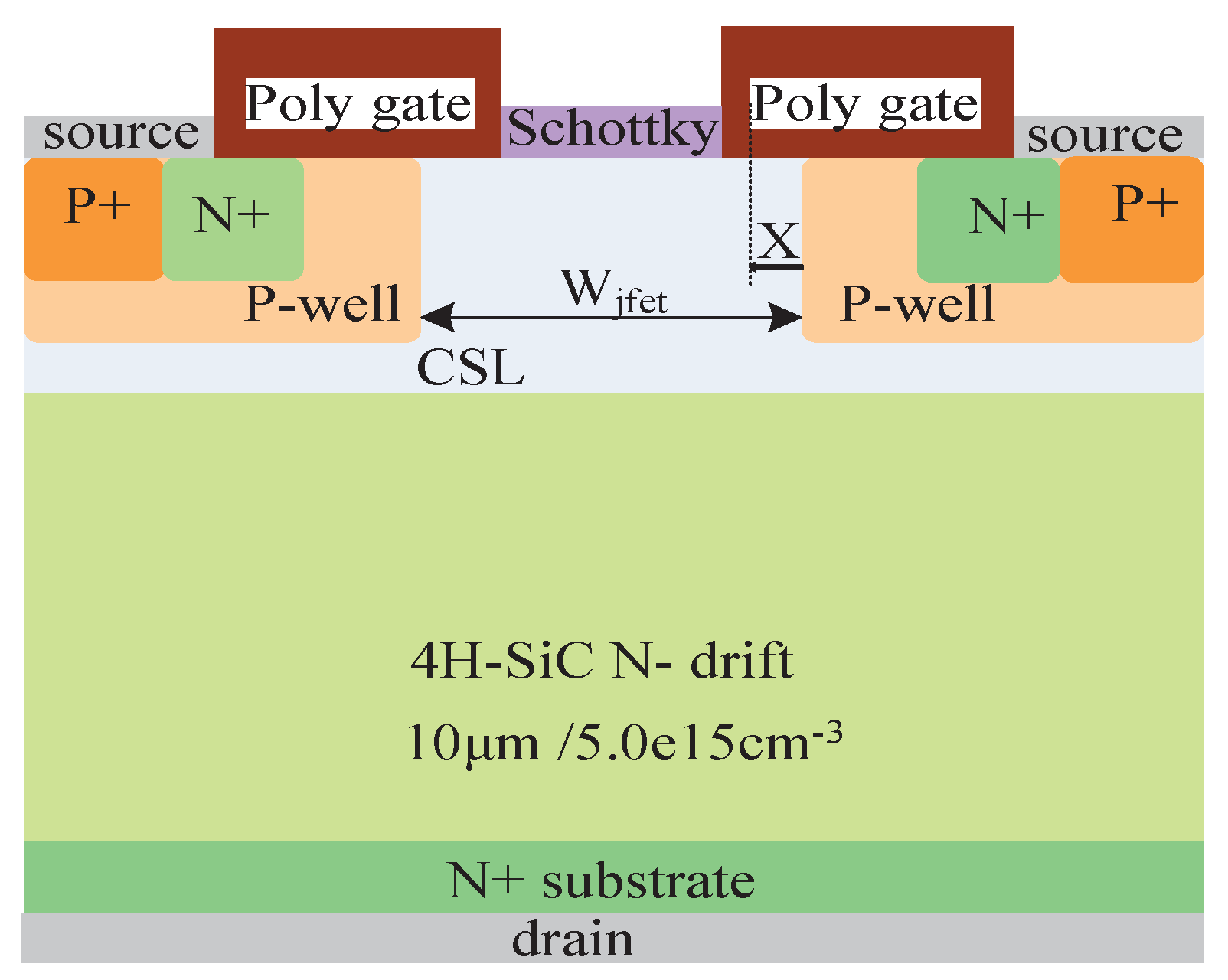
Figure 2.
Incident positions in different regions.
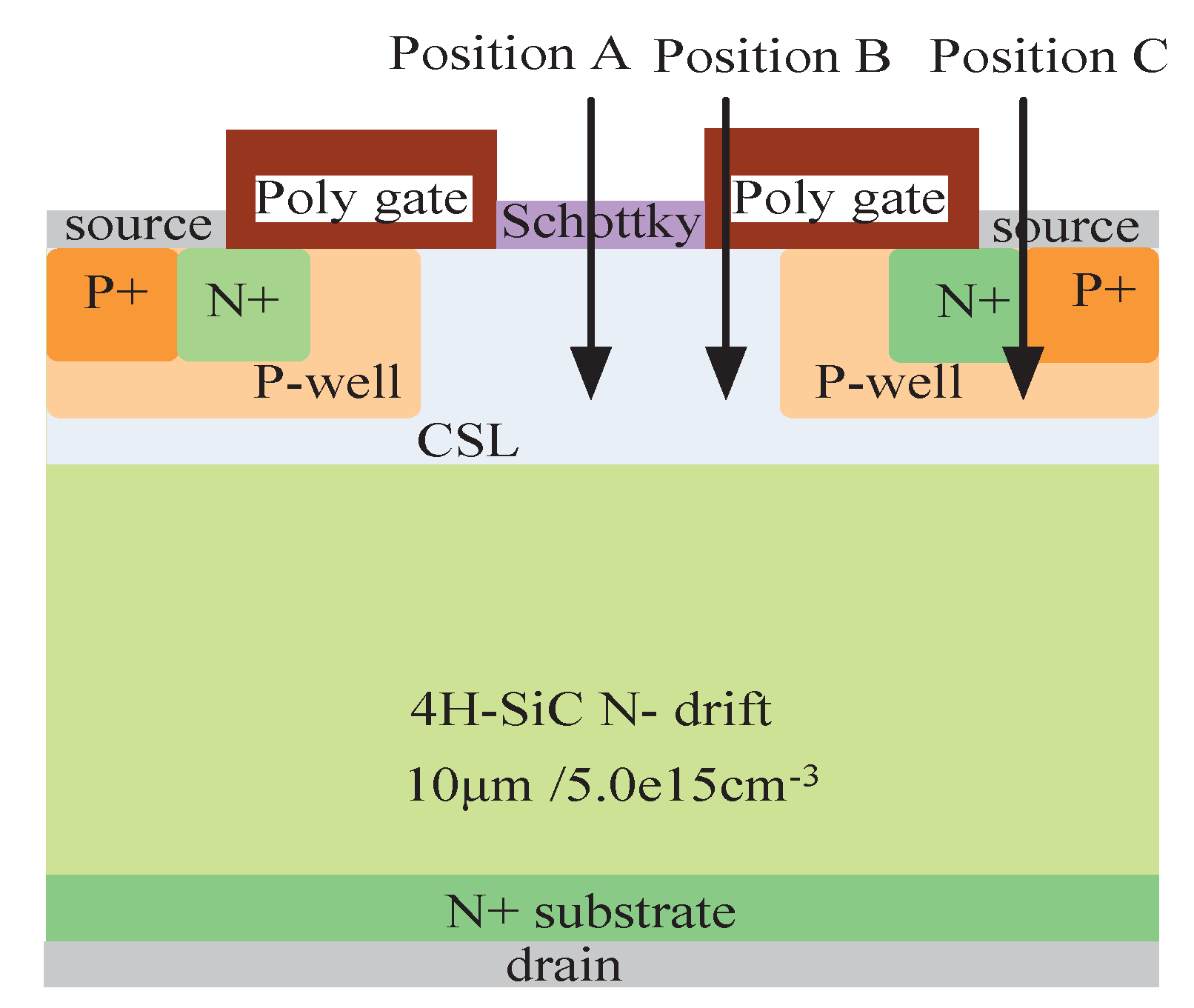
Figure 3.
Transient current variation curves at different incident positions in different regions.
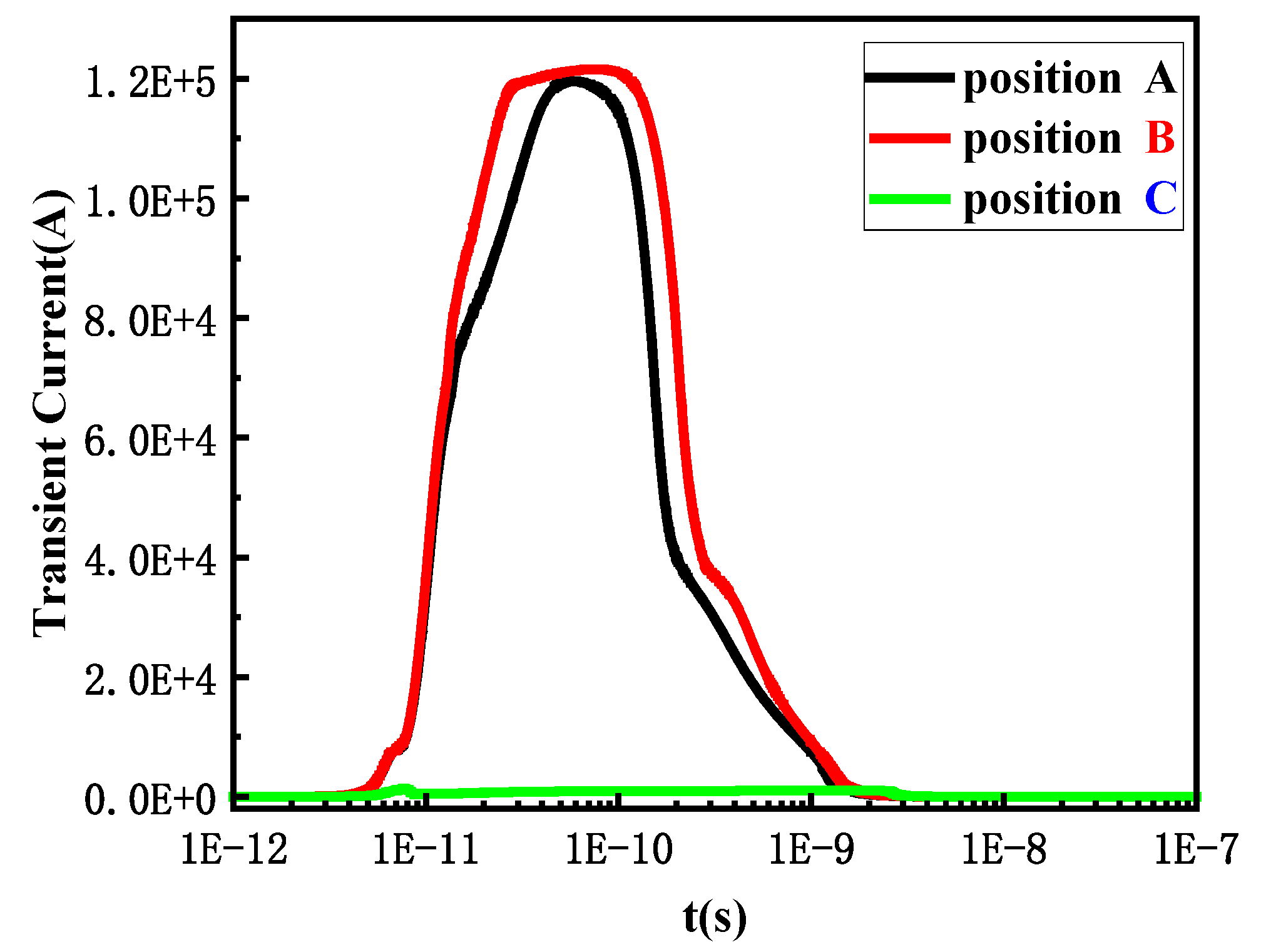
Figure 4.
(a)Transient current curves of heavy ions incident from position B under different biases; (b)incident position B.
Figure 4.
(a)Transient current curves of heavy ions incident from position B under different biases; (b)incident position B.
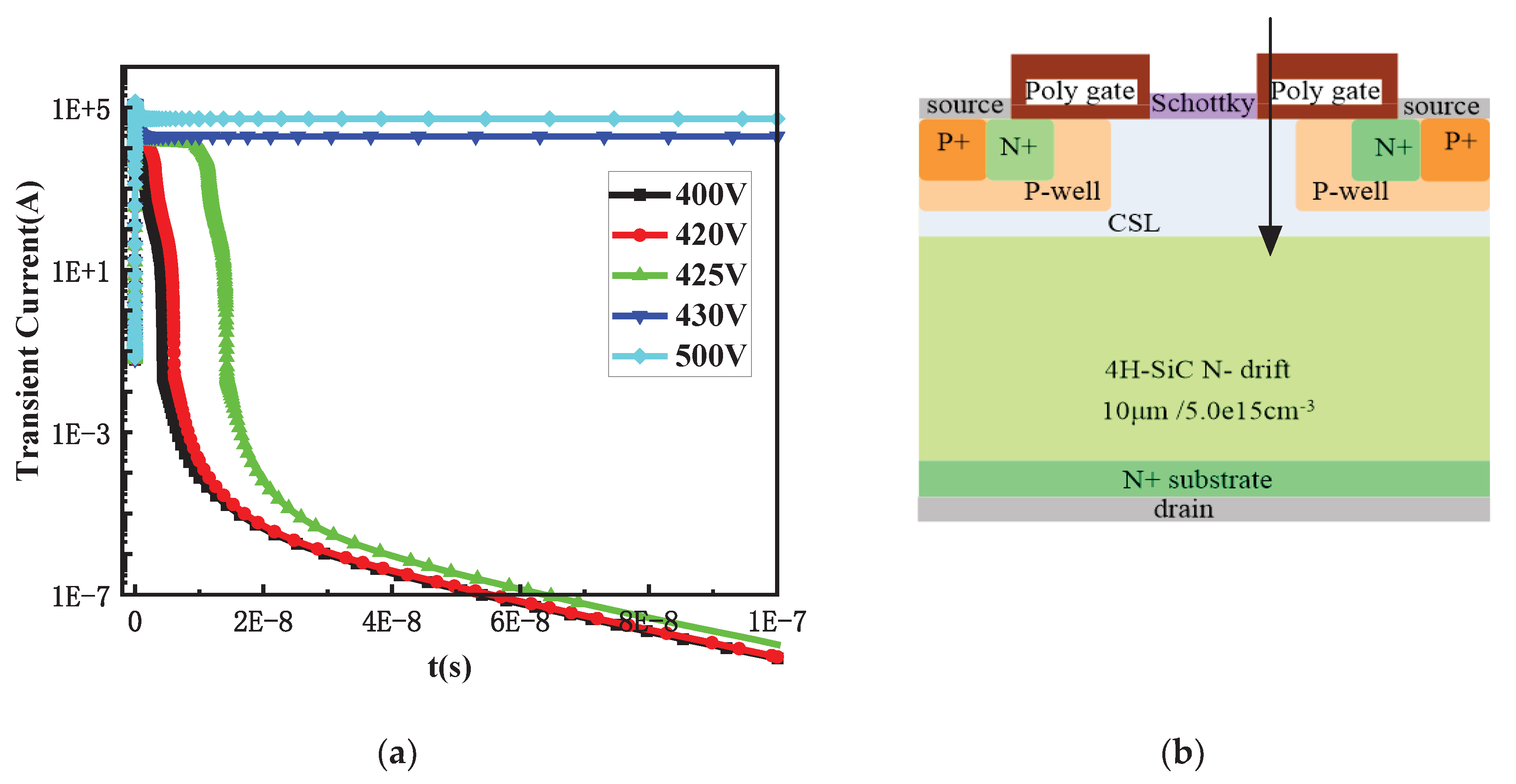
Figure 5.
Distribution trend of electricfield peak transfer during SEB(VDS=450V:(a) 1ps; (b) 10ps; (c) 100ps; (d) 10−7s; (e) Enlarged diagram of electricfield distribution in the oxide layer at 10ps; (f) Enlarged diagram of electricfield distribution in the oxide layer at 100ps.
Figure 5.
Distribution trend of electricfield peak transfer during SEB(VDS=450V:(a) 1ps; (b) 10ps; (c) 100ps; (d) 10−7s; (e) Enlarged diagram of electricfield distribution in the oxide layer at 10ps; (f) Enlarged diagram of electricfield distribution in the oxide layer at 100ps.
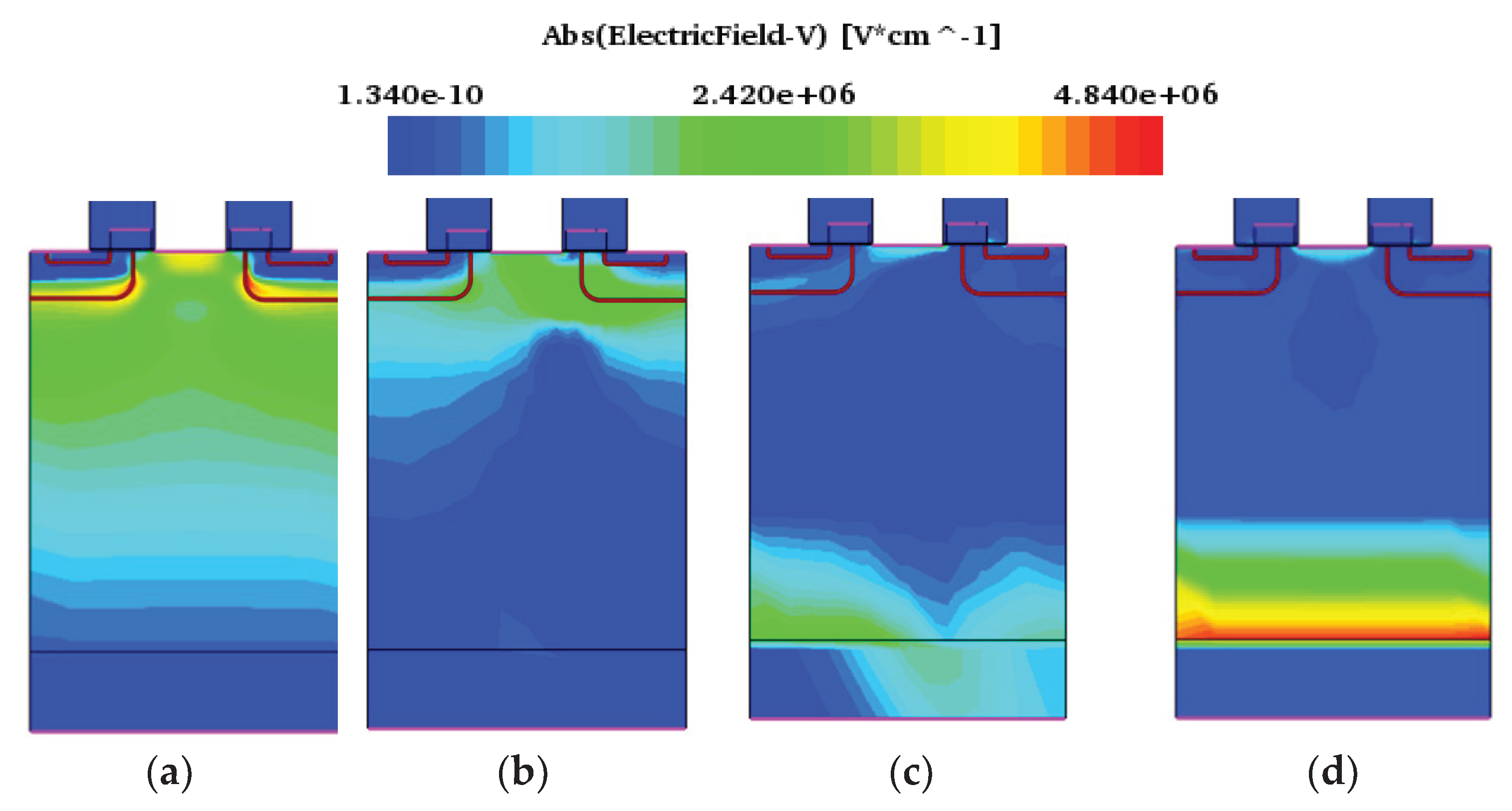
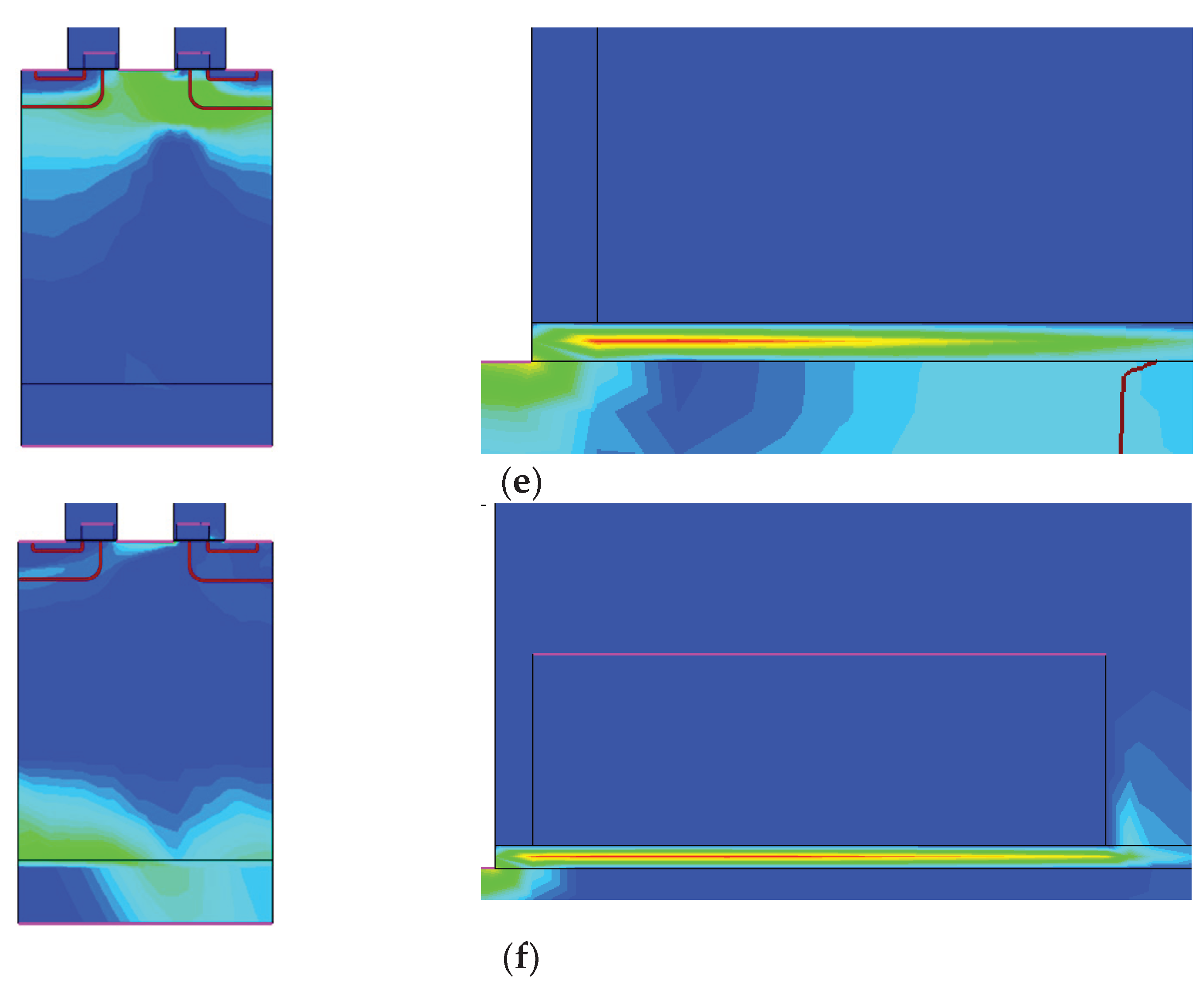
Figure 6.
Schematic diagram of the expansion positions of different P+body contact areas.
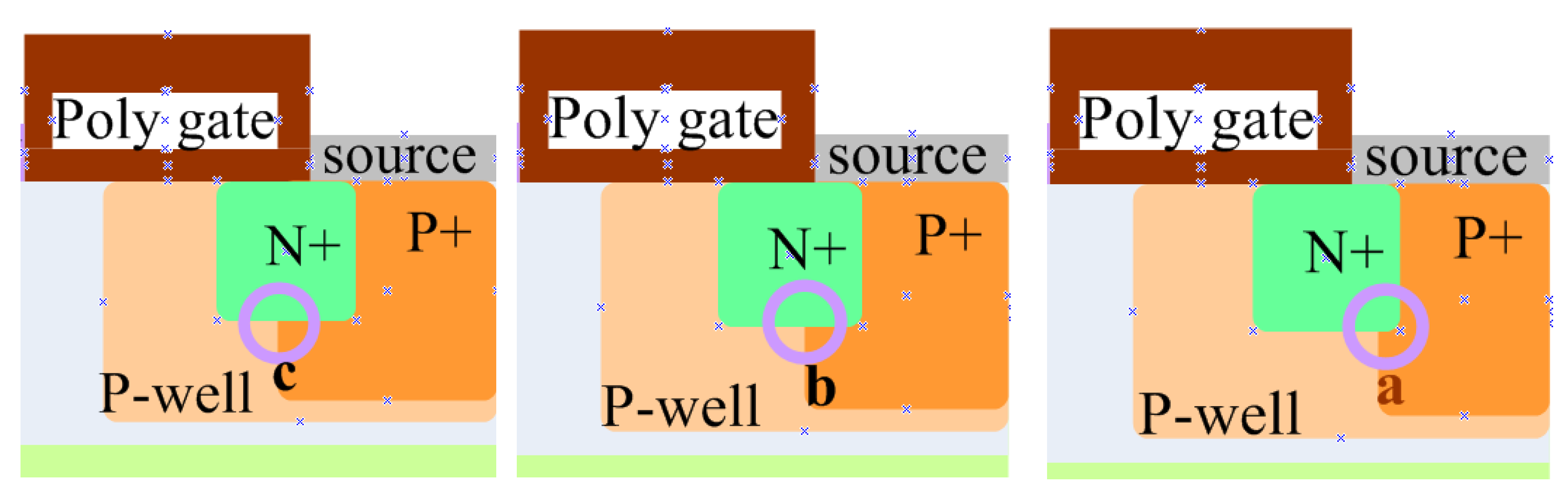
Figure 7.
(a)Transient current curve of the extended position b in the P+body contact area; (b)incident position C.
Figure 7.
(a)Transient current curve of the extended position b in the P+body contact area; (b)incident position C.
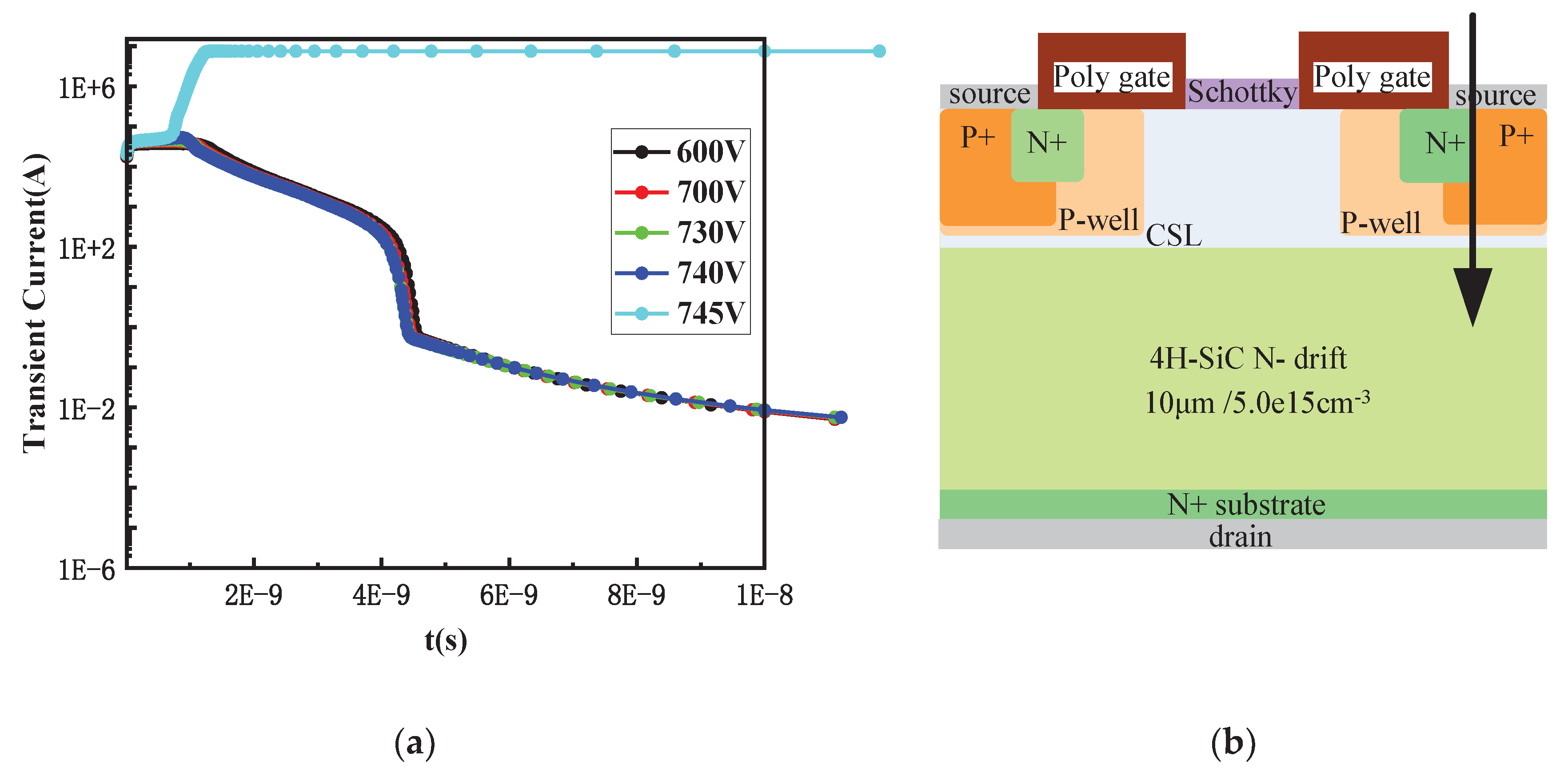
Figure 8.
structure with multi-layer N-type interval buffer layer.
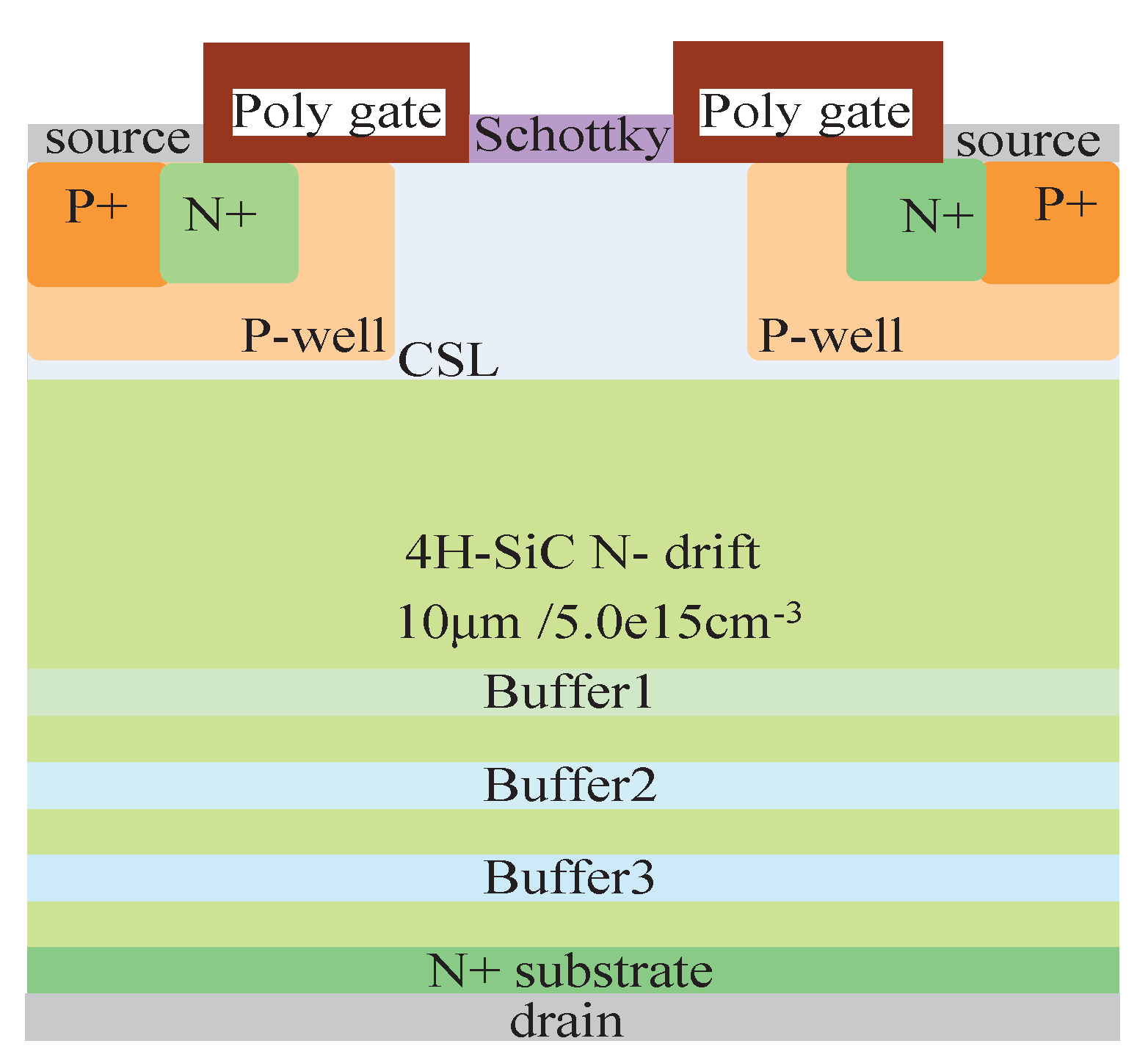
Figure 9.
(a) curves under different bias voltages after optimized design of buffer2 and buffer3; (b)incident position A.
Figure 9.
(a) curves under different bias voltages after optimized design of buffer2 and buffer3; (b)incident position A.
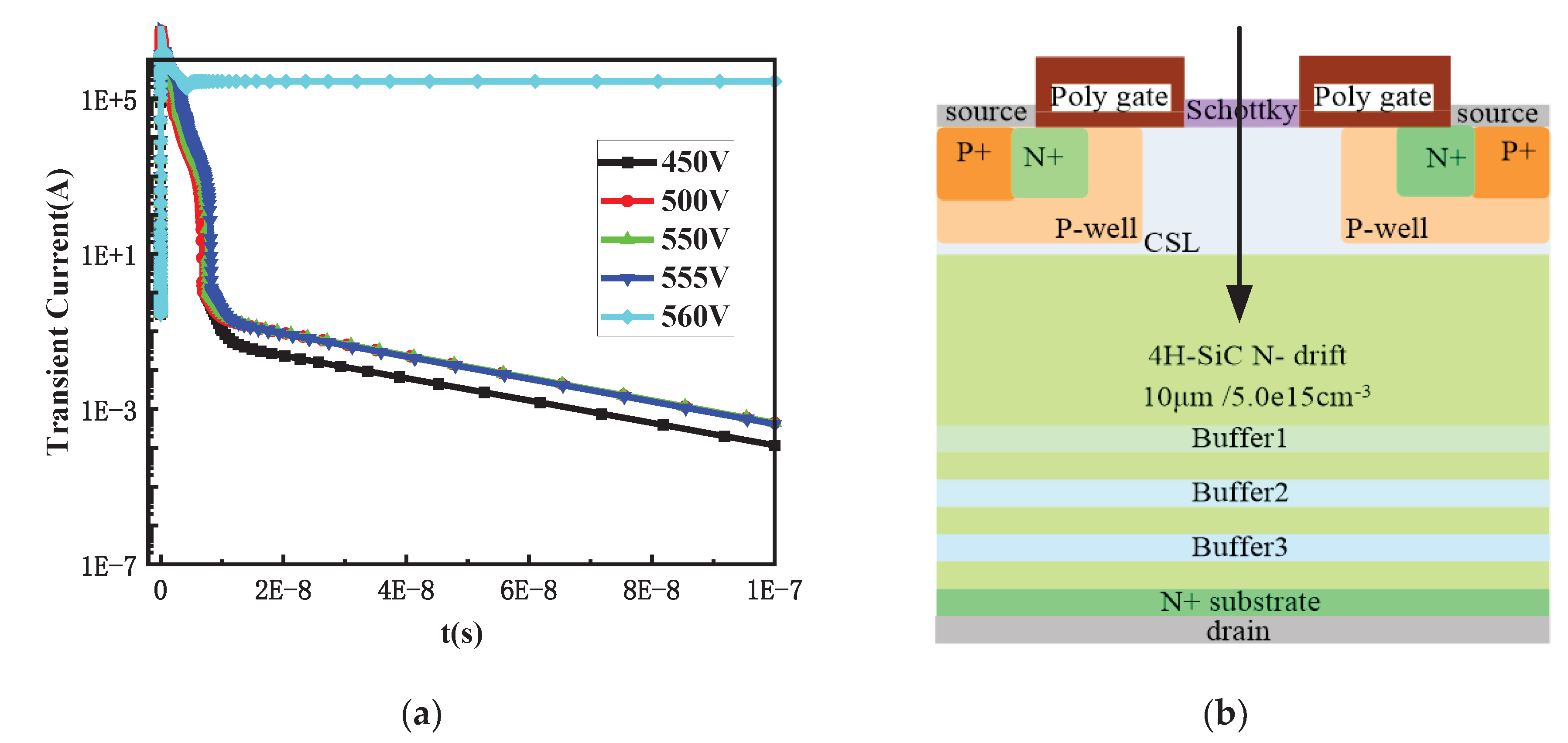
Figure 10.
Electricfield distribution before or after SEB with buffer layer design.
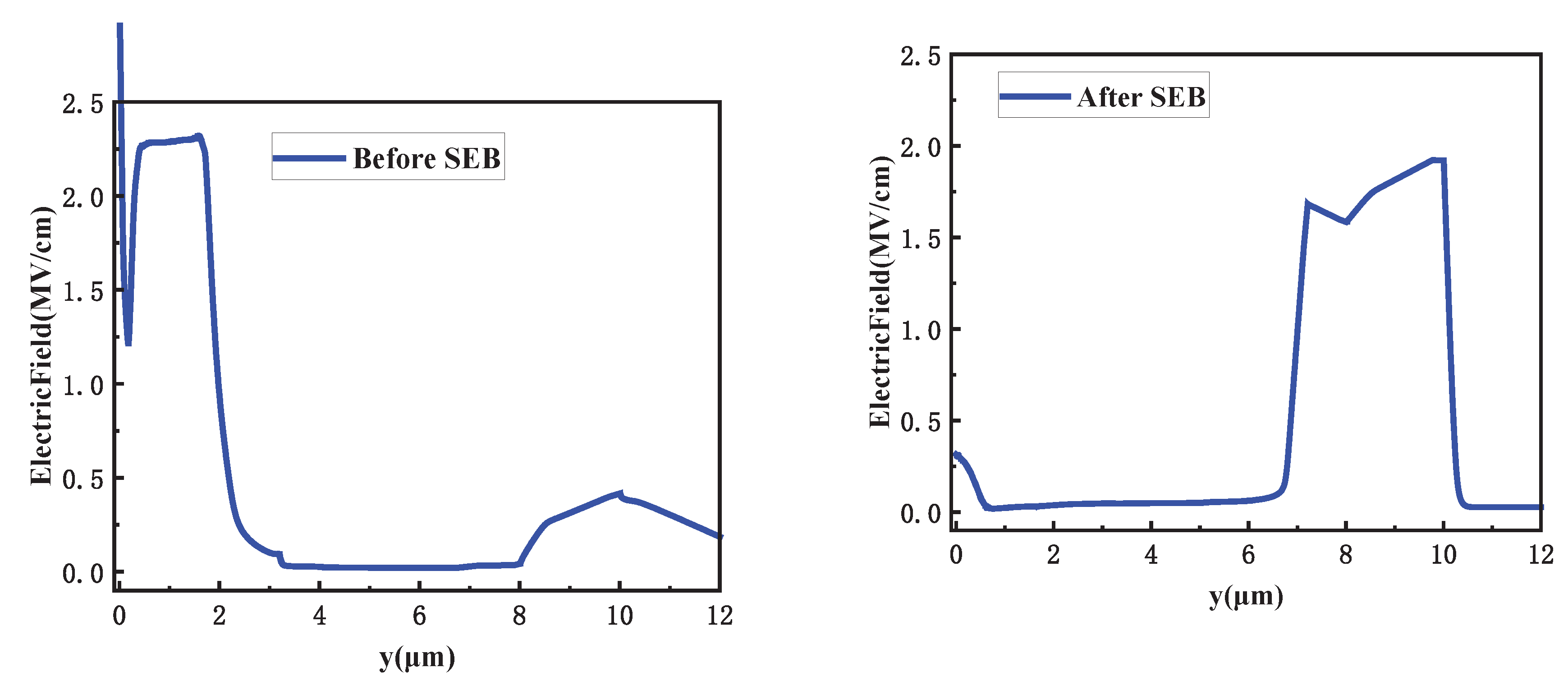
Figure 11.
Electricfield distribution transfer for SEB with buffer layer design: (a)1ps; (b)10ps; (c)1000ps; (d)10−7s.
Figure 11.
Electricfield distribution transfer for SEB with buffer layer design: (a)1ps; (b)10ps; (c)1000ps; (d)10−7s.
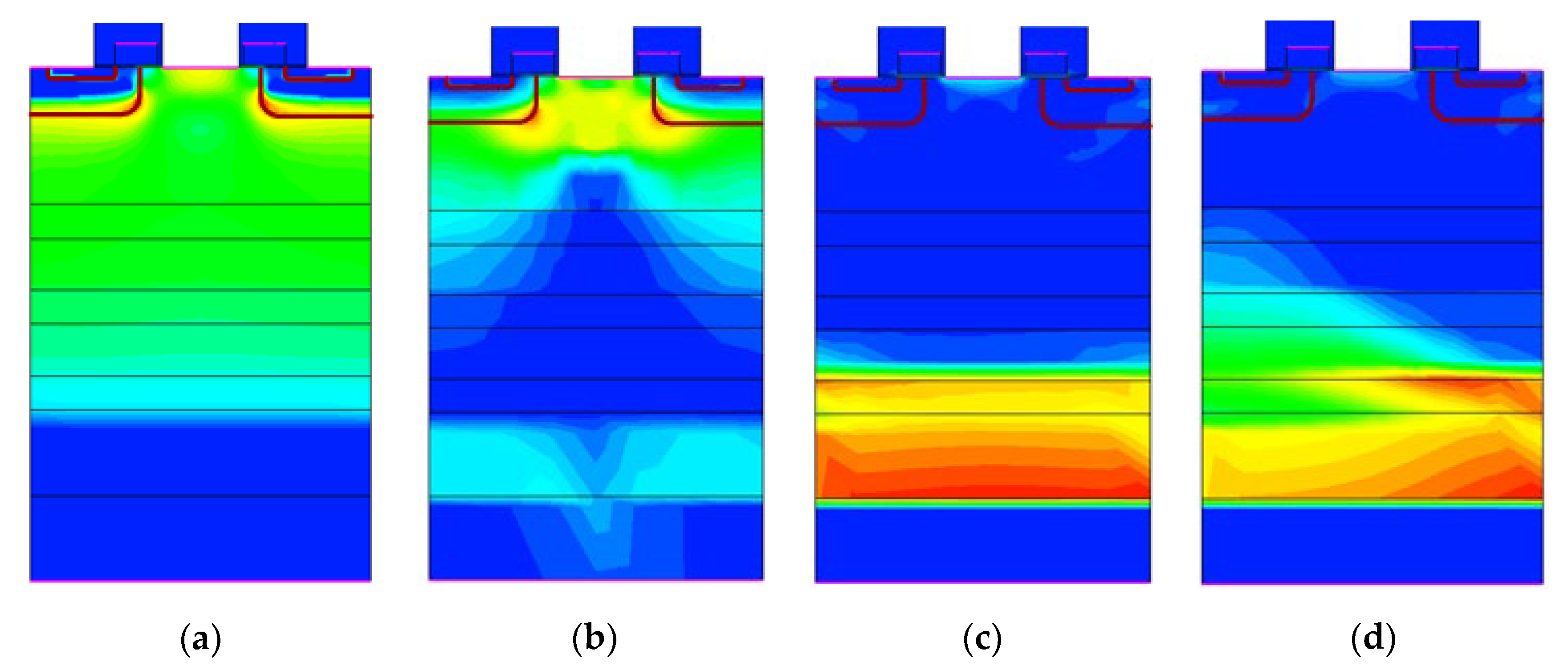
Figure 12.
Device structure after comprehensive reinforcement optimization.
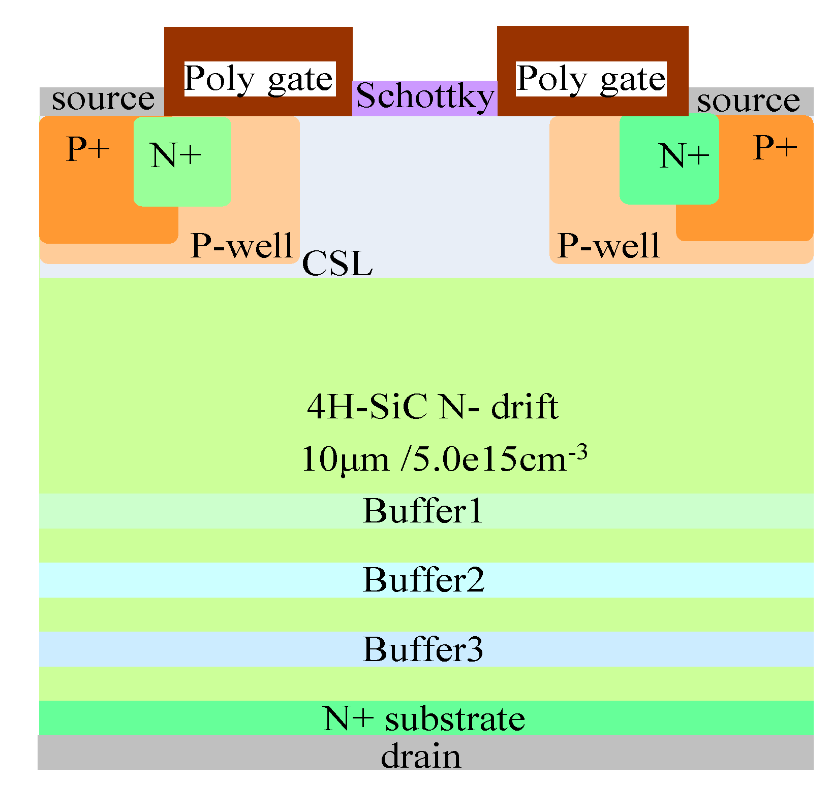
Figure 13.
Equivalent circuit in different areas after comprehensive reinforcement.
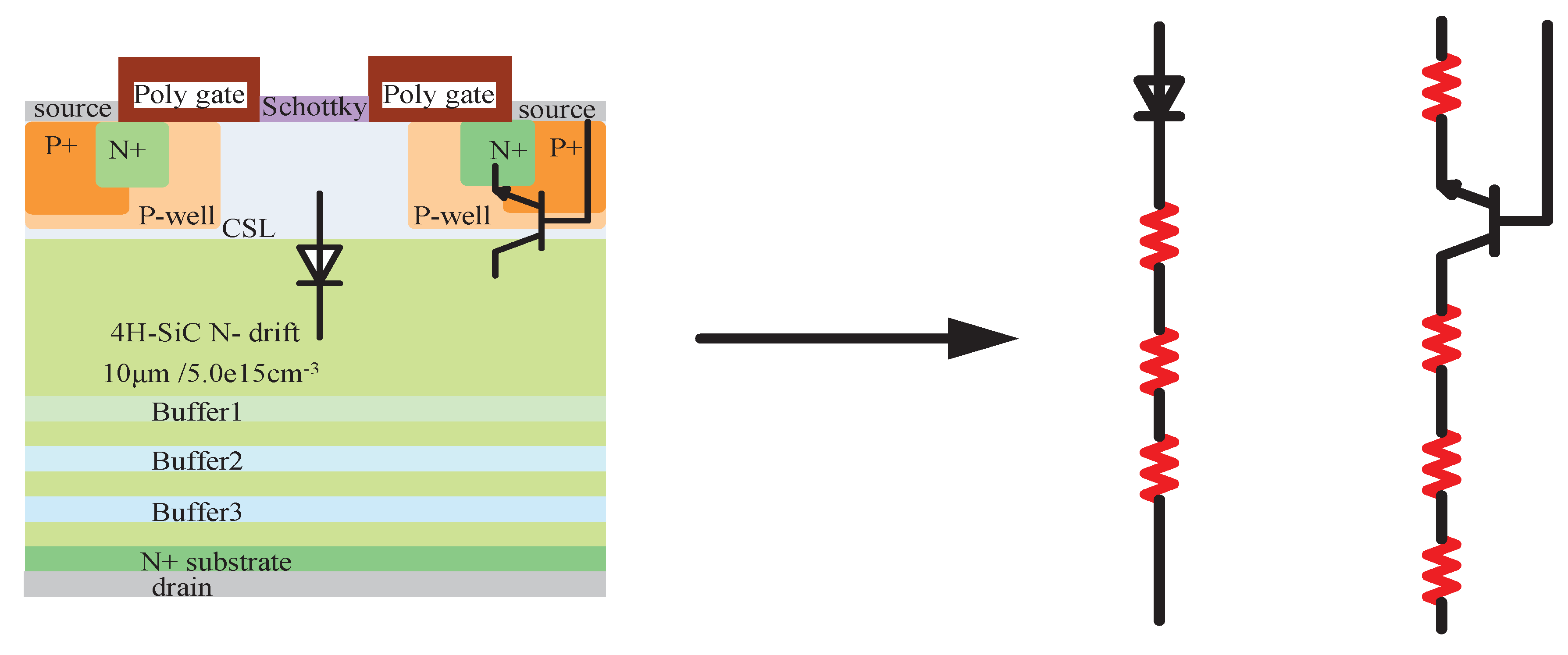

Table 1.
SEB threshold voltage at different incident positions.
| Incident position | Position A | Position B | Position C |
|---|---|---|---|
| SEB threshold voltage (V) | 430 | 430 | 640 |
Table 2.
Impact of P+body contact area extension on device performance.
| Expand Location | Unexpanded | a | b | c |
|---|---|---|---|---|
| SEB threshold voltage (V) | 640 | 735 | 740 | 745 |
| Third quadrant conduction voltage(V) | 1.283 | 1.283 | 1.283 | 1.312 |
| Breakdown voltage of the device(V) | 1632.935 | 1641.787 | 1642.935 | 1642.888 |
Table 3.
Changes in device characteristics after buffer layer reinforcement design.
| Doping concentration of buffer1(cm−3) | - | 1.0×10¹⁵ | 6.0×10¹⁵ | 8.0×10¹⁵ | 1.0×10¹⁶ | 1.5×10¹⁶ |
|---|---|---|---|---|---|---|
| SEB threshold voltage (V) | 430 | 440 | 440 | 440 | 440 | 440 |
| Breakdown voltage of the device(V) | 1632.935 | 1392.659 | 1359.178 | 1342.803 | 1333.024 | 1293.024 |
Table 4.
Changes in device characteristics after optimized design of buffer2 and buffer3.
| Doping concentration of Buffer2(cm−3) | 1×10¹⁷ | 1×10¹⁷ | 3×10¹⁷ | 3×10¹⁷ |
|---|---|---|---|---|
| Doping concentration of Buffer3(cm−3) | 8×10¹⁷ | 1×10¹⁸ | 3×10¹⁸ | 6×10¹⁸ |
| SEB threshold voltage (V) | 430 | 440 | 505 | 555 |
| Breakdown voltage of the device(V) | 1392.659 | 1392.659 | 1392.659 | 1392.659 |
Table 5.
Changes in characteristics before or after comprehensive reinforcement design.
| Before or after reinforcement | Unreinforced | Case3 |
|---|---|---|
| SEB threshold voltage for position C(V) | 640 | 635 |
| SEB threshold voltage for position A(V) | 430 | 570 |
| Breakdown voltage of the device(V) | 1632.935 | 1403.135 |
Table 6.
Changes in characteristics before or after different reinforcement designs.
| Before or after reinforcement | Unreinforced | Case1 | Case2 | Case3 |
|---|---|---|---|---|
| SEB threshold voltage for position C(V) | 640 | 740 | -- | 635 |
| SEB threshold voltage for position A(V) | 430 | -- | 555 | 570 |
| Breakdown voltage of the device(V) | 1632.935 | 1642.935 | 1392.659 | 1403.135 |
Disclaimer/Publisher’s Note: The statements, opinions and data contained in all publications are solely those of the individual author(s) and contributor(s) and not of MDPI and/or the editor(s). MDPI and/or the editor(s) disclaim responsibility for any injury to people or property resulting from any ideas, methods, instructions or products referred to in the content. |
© 2024 by the authors. Licensee MDPI, Basel, Switzerland. This article is an open access article distributed under the terms and conditions of the Creative Commons Attribution (CC BY) license (http://creativecommons.org/licenses/by/4.0/).
Copyright: This open access article is published under a Creative Commons CC BY 4.0 license, which permit the free download, distribution, and reuse, provided that the author and preprint are cited in any reuse.


