
Submitted:
01 April 2024
Posted:
01 April 2024
You are already at the latest version
Abstract
Tellurium exhibits exceptional intrinsic electronic properties. However, investigations into the modulation of tellurium's electronic properties through physical modification are notably scarce. Here, we present a comprehensive study focused on the evolution of the electronic properties of tellurium crystal flakes under plasma irradiation treatment by employing conductive atomic force microscopy and Raman spectroscopy. The plasma-treated tellurium experienced a process of defect generation through lattice broken. Prior to the degradation of electronic transport performance due to plasma irradiation treatment, a remarkable observation emerged: in the low-energy region of hydrogen plasma-treated tellurium, a notable enhancement in conductivity was unexpectedly detected. The mechanism underlying this enhancement in electronic transport performance was thoroughly elucidated by comparing it with the electronic structure induced by argon plasma irradiation. This study not only fundamentally uncovers the effects of plasma irradiation on tellurium crystal flakes, but also unearths an unprecedented trend of enhanced electronic transport performance at low irradiation energies when utilizing hydrogen plasma. This abnormal trend bears significant implications for guiding the prospective application of tellurium-based 2D materials in the realm of electronic devices.
Keywords:
tellurium crystal flake
; plasma irradiation
; tunnelling current
; conductive atomic force microscopy (CAFM)
; band gap
1. Introduction
2D (2D) single crystal materials have many applications in the fields of electronics, optics, magnetism and other fields due to their quantum confinement effect in z-space [1,2,3,4,5,6]. The exotic properties of the 2D materials attracted tremendous focus in scientific research community in recent years, especially in the field of electronics. Compared with traditional semiconductor materials represented by silicon, most of the 2D materials have some shortcomings for their intrinsic electronic properties. Graphene cannot be used as an ideal logic device with high current switching ratios due to its zero band gap [2], on the other hand, most transition metal chalcogenide compounds with appropriate natural band gaps can have high current switching ratios in logic devices, but they are difficult to achieve high mobility [7]. Thus, 2D materials that simultaneously meet the characteristics of high current on-off ratio and high mobility have been one of the key focuses of research in 2D electronic materials in recent years. Among them, tellurium, as a natural single-element-based 2D material with appropriate band gap, has been demonstrated to present excellent intrinsic electronic properties, with high current switching ratio (~ 106) and high carrier mobility (~ 700 cm2V-1s-1) [8,9,10,11], and it also shows relatively good stability in ambient air at room temperature. The band gap is ~ 1 eV and 0.35 eV for its monolayer and bulk, respectively [10,12]. The bulk tellurium can be diversified fabricated into crystals through methods such as hydrothermal approach [10], chemical vapor deposition (CVD) [13], and physical vapor deposition (PVD) [14]. Tellurium has a wide range of potential applications such as field effect devices [10,15], infrared devices [16,17], photodetectors [16,18,19], piezoelectric devices [20,21]. Although tellurium possesses excellent intrinsic electronic properties, it is relatively lack of research on the stability of its own crystal structure and electronic structure modulation beyond its intrinsic electronic properties. Through physical modification, especially the method of plasma-based surface treatment, it can not only study the stability of its crystal structure, but also reveal the evolution of electronic properties. Previously, plasma treatment has been commonly used to modify the crystal structure and electronic properties for 2D materials for both fundamental studies and practical applications [22,23,24].
For tellurium, the plasma irradiation related papers are rare. In this work, the surface structure modification of tellurium crystal flakes has been achieved through the hydrogen plasma (HP) and Ar plasma (AP) irradiation treatments, respectively. Using the contact mode of conductive atomic force microscopy (CAFM) [25], the evolution of the electronic properties of the plasma irradiated tellurium corresponding to its surface structure modification, has been revealed by scanning the contact tunnelling current properties biased between a conductive tip and the tellurium flake. Combined with Raman spectroscopy study, it was confirmed that the tellurium crystal flake did not undergo phase transformation or chemical change during the plasma irradiation treatment, but the crystal structure would be broken gradually under certain energy irradiation. It is also found in this work that through HP treatment, the low irradiation energy region can be used to improve the transport performances of tellurium crystal, but no corresponding improvement window was found by AP treatment.
2. Materials and Methods
2.1. Preparation of Tellurium Flakes
In a typical synthesis case, 100mg of sodium tellurite powder and 498mg of polyvinylpyrrolidone powder were weighed, and then added them with 33ml of deionized water, 1ml of hydrazine hydrate and 1ml of ammonia aqueous solution respectively. After fully stirring, the mixed solution was added to a autoclave reactor to keep at 180 ℃ for 40 hours. The reaction results in a solution of tellurium flakes, which is added to a centrifuge tube for repeated centrifugation. After ultrasonic washing to remove surface impurities, the remaining solution is filtered to obtain a relatively pure sample of tellurium flakes.
2.2. Preparation of Tellurium Devices to Be Tested
The samples of tellurium flakes were peeled repeatedly with tape, and the tape obtained after peeling was tightly bonded with PDMS (polydimethylsiloxane), so that a small amount of tellurium flakes was attached to PDMS, and the target sample can be located under the optical microscope.
After the Si/SiO2 wafer chip was washed with acetone, the photolithography process was then performed on the silicon wafer to obtain an area covered with large gold electrodes. The target tellurium flakes on PDMS were transferred respectively to the areas covered by gold electrode and Si/SiO2 wafer chip through a two-dimensional material transfer platform. Then the conductive silver paste is used to connect the gold electrode and the metal-based CAFM holder to ensure good conductivity between the gold electrode and the CAFM holder.
2.3. Plasma Treatment of Tellurium Flakes
A plasma surface processor was used to connect to the hydrogen and argon sources, respectively. The prepared tellurium device was irradiated by plasma treatment at a pressure of about 0.1mbar. The plasma irradiation treated devices were characterized by conductive atomic force microscopy (CAFM), Raman spectroscopy and optical microscopy.
3. Results and Discussion
3.1. Crystal Morphology and Band Gap Characterization for the Pristine Tellurium Flakes
Tellurium powder with nano flake microstructure were prepared by hydrothermal reaction according to the similar recipe as the method reported previously [10]. Figure 1a shows a scanning electron microscope (SEM) image of a tellurium sample obtained after hydrothermal processing. Most of the tellurium crystals are in the microstructural shape of rectangular sheets or rods, stacked randomly on the substrate. According to the X-ray diffraction (XRD) result, it shows a series of feature diffraction peaks for the tellurium sample, of which the positions of the peaks are completely consistent with the ideal tellurium structure (refer to the PDF card as a comparison shown in Figure 1b). Among them, the (100) and (101) diffraction peaks are particularly strong, and the full width of half maximum of the peaks are as low as 0.22o and 0.21o, respectively, indicating that the synthesized crystals have good crystallinity. Based on the characterization of the crystal structure, the tellurium sample has obvious optical absorption feature peaks in the infrared region as shown in Figure 1c. The corresponding optical band gap can be obtained through fitting on the basis of Kubelka–Munk formula conversion [26,27]. The most prominent absorption peak shown in the yellow box of Figure 1c was chosen to be converted, as can be seen in Figure 1d, the optical band gap of tellurium is ~0.39eV. The result is close to the band gap of the reported bulk tellurium, indicating the intrinsic electronic structure properties that is owing to the good crystalline quality.
3.2. Study on the Evolutions of the Structure and Electronic Properties of Tellurium Crystal Flake under Plasma Treatment
The HP treated tellurium crystal flake surface is schematically shown in Figure 2a. The optical images were used to record the change of the tellurium crystal surface structure with gradually increased HP treatment power and duration (Figure 2b). For pristine tellurium before undergone HP treatment, there are three Raman active modes can be seen in the 0th curve in Figure 2c, which are the mode A1 (chain expansion in the ab plane), E1 (a- and b-axis rotation), and E2 (asymmetric stretching mainly along c-axis) [28]. At the beginning with relatively low HP irradiation power as 10W, 20W and 30W, the crystal structure evolution did not show obvious changes compared to that of the pristine sample (see optical images in Figure 2b 1-6). Each of the corresponding Raman spectrum always clearly presents almost the same feature as that of the pristine tellurium (see the 1st-6th curves in Figure 2c), which illustrates that HP irradiation with low power and duration is relatively” gentle” for tellurium flakes. When the plasma irradiation power further increased to 60W, the optical images show that the tellurium crystal starts undergone obvious structural damage on the surface after a total treatment duration of 90 seconds at this power (see the optical image for the 7th treatment in Figure 2b). This obvious change may be due to the fact that the energy accumulation on the tellurium surface during HP treatment has reached the crystal structure broken threshold. Therefore, once the irradiation power and energy exceeding a certain value, the tellurium flake will undergo structural damage. HP treatment for the same tellurium sample under subsequent higher power conditions (100W) resulted in more obvious microstructural damage to the surface (see optical images after the 7th treatment in Figure 2b). However, it is noted that no observed additional Raman peaks appeared in this sample even it has been irradiated by HP with the power of 100W and duration of 90s (see the 8th-10th Raman spectra in Figure 2c). We basically infer that the effect of HP on tellurium mainly causes microscopic crushing at the physical level, but does not give rise to the structural phase transformation or introduce any chemical change.
Meanwhile, the HP induced evolution trend of tellurium surface roughness and bulk thickness with respect to the irradiation energy has been systematically studied through the atomic force microscopy imaging system. It can be seen from Figure S1c that regardless of the HP irradiation power, the thickness of the tellurium flake area that basically shown a thinning trend, and accompanied by a slight but monotonically increase in surface roughness (Figure S1d). It should be noted that the high-power irradiation process given rise to the obvious damage to the sample flake under optical microscope observation, thus the flake component that has not been disappeared on the substrate was chosen for AFM study comparison.
Though the tellurium crystal flake does not undergo structure phase transformation or chemical change under HP treatment, the lattice broken caused the flake crystal destruction by the increased irradiation energy is unavoidable. As tellurium is well-known for its electronic properties, thus it is deserved to pay attention on the evolution of electronic properties under HP irradiation. Here, we transfer another tellurium flake onto a gold electrode substrate, and based on the contact mode of conductive atomic force microscopy (CAFM), the tunnelling current was scanned through the contact bias between the conductive tip and the tellurium flake to reveal the electronic properties and band gap evolution relationship under plasma irradiation [20]. Figure 3a and b give the CAFM contact mode probed IV curves of the tellurium flake under HP treatment with increasing irradiation energies. Surprisingly, the effect of HP irradiation bombardment on the tellurium lattice does not show a monotonous decrease trend. In the process of HP irradiation with relatively low power and a shorter duration (accumulated as low irradiation energy region), the conductivity of the tellurium flake is in a monotonous rising trend. When the irradiation power further increases, the tunneling current begins to decrease rapidly (Figure 3b). On the other hand, it is worth noting that Faisal Shahzad et al. also significantly improved the electron field emission performance of tellurium nanorods arrays grown perpendicular to the substrate (dropping from 6.22 V/μm to 3.25 V/μm) by HP irradiation treatment, and the authors attributed this improvement to the fact that HP produces numerous abrupt-tips, which increases its emission current density and thereby enhances its conductive properties [29]. In this work, the optical images clearly indicate that the tellurium crystal flake surface structure has not been damaged by HP irradiation energy accumulation at relatively low power (see the optical images for the first 6th HP treatments in Figure 2b). As the HP irradiation process equals to the hydrogen ion implantation effect, it is inferred that such ion implantation at low-energy region may cause an effective charge doping effect rather than breaking the structural lattice, resulting the increase in its conductivity. As a consequence, the HP treatment with low-energy shows an overall increase in tunnel current.
To confirm this viewpoint, we parallelly use inert atom argon as the plasma gas source to irradiate the tellurium crystal flake in the similar way as that of using HP. As can be seen in Figure S2a, similar to the HP treatment of tellurium surface, in the low irradiation energy region, its surface structure still does not appear obvious changes (Fig S2a 0-4). As the AP irradiation treatment power and energy increase, more and more areas on its surface begin to suffer structural damage (Figure S3a 5-8). It is worth noting that during the entire irradiation process, the three intrinsic Raman feature peaks of tellurium (A1, E1 and E2) did not change significantly (i.e.: sharpening or broadening of FWHM; blue- or red-shift of peak positions), and also no additional new Raman vibration peaks appeared (Figure S2b), which means that even using the high-energy plasma irradiation, it only destroyed the microstructure of the flake by breaking its crystal lattice, but did not give rise to new structural phase transformation or chemical change. The AP treatment did not cause the changes of Raman feature which is very similar to the HP irradiation effect as discussed earlier. However, the AP irradiation induced tunnel current response of the tellurium crystal flake based on the contact bias scanned between the conductive tip and the tellurium surface not only shows a monotonic decreasing trend in the later stage of irradiation with high-power, but the tunnel current also directly starts to show the dramatical decreasing trend at the early stage with low-power irradiation (Figure 3c).
To get more intuitively understanding of the above analyzed results, The evolutions of tellurium conductance with HP and AP irradiation treatment are shown in Figure 3d. As the treatment energy increases in the low-power region (see the blue layer region in Figure 3d, and it is defined as stage-1 treatment), the conductance of HP irradiated tellurium flake increases significantly. As a comparison, it is very clear to see that even at the stage-1 treatment region, the conductance of AP irradiated tellurium flake shows a dramatical decreasing trend. This may be due to the fact that Ar is a much heavier element, and even with lower power AP treatment, the bombardment effect on the tellurium lattice is still strong. That is to say, compared with HP, AP treatment is more effective in breaking the crystal lattice for tellurium flakes even at the low-power-based stage-1 irradiation region. On the other hand, the element Ar is more neutral than H, thus AP treatment cannot easy to provide a charge doping effect as similar as that of HP treatment for the tellurium flake. It infers that AP treatment only gives rise to the bombardment effect to break the crystal lattice but do not have the compensated positive impact on its conductivity properties by charge doping. Furthermore, compared with HP, AP treatment requires less irradiation energy to decrease the conductivity of pristine flake by 1-order (see the red and black stars shown in Figure 3d), which should also be attributed to the fact that AP treatment gives a "heavy element" bombardment effect on tellurium flake compared to that of the HP treatment.
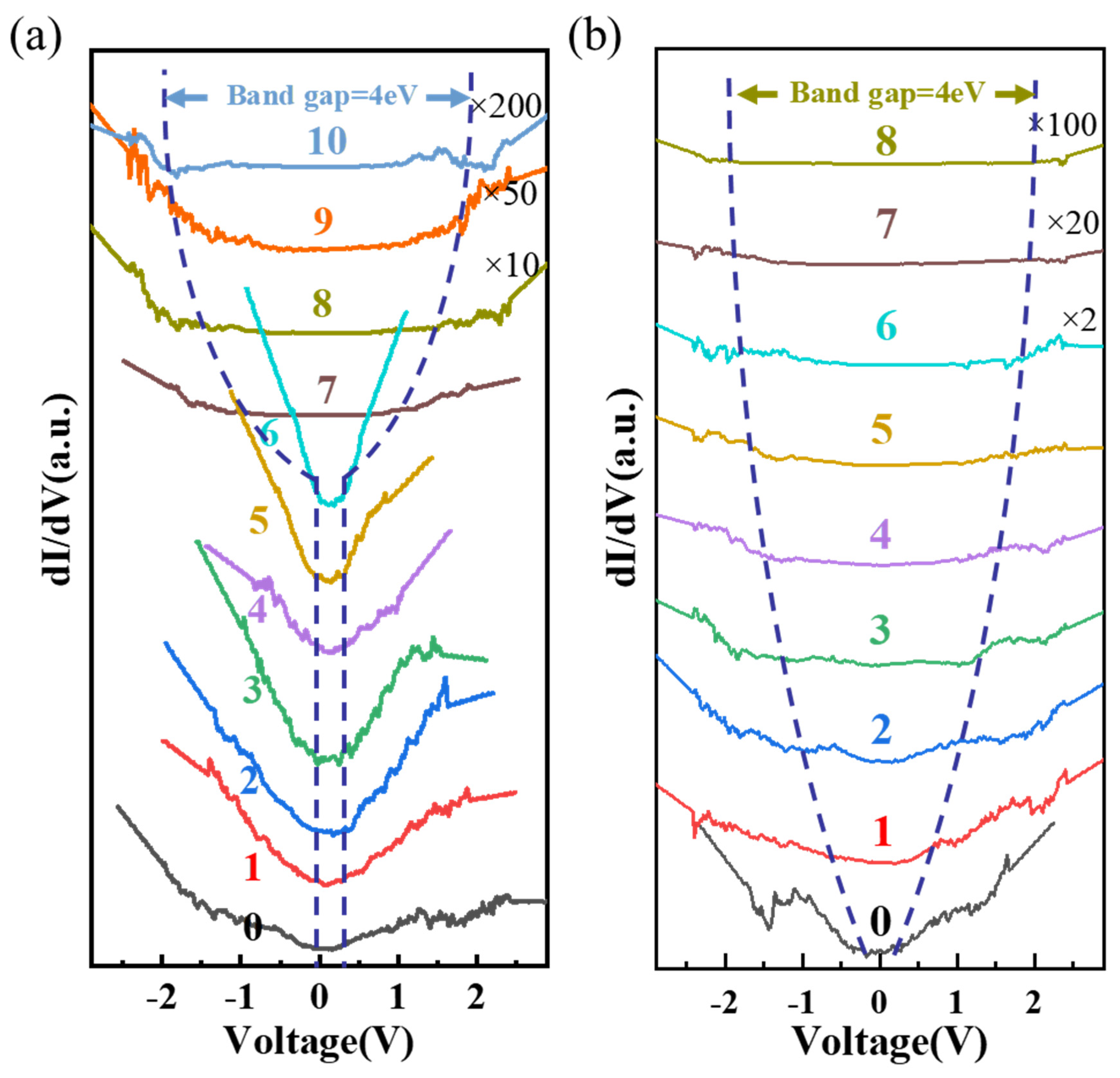
In addition to study the plasma treatment modulated transport properties of tellurium crystal flake through measuring the tunnel current (I) based on contact bias (V) scanning between the conductive tip and the tellurium flake, the evolution of the band gap of the tellurium crystal flake with respect to the plasma treatment have also been studied. In fact, the slope of the I-V curve (dI/dV) at each voltage (V) corresponds to the electron density (LDOS) of states at the tip probed position of the sample. It means that using such scanning tunneling spectroscopy (STS) on the basis of dI/dV -V, the zero LDOS region in the STS spectrum can be used to reflect the band gap of conductive tip probed tellurium flake. Figure 4 shows the STS spectra for the HP and AP irradiation treated tellurium flake, respectively (the STS spectra are derived from the smoothed I-V curves from Figure 3). The evolution of the tellurium flake band gap with respect to the HP irradiation treatment is schematically shown in Figure 4a. It can be seen by the 0th curve in Figure 4a that the band gap is about 0.35eV for pristine tellurium, which is close to the band gap of the originally synthesized tellurium powder derived from infrared absorption fitting (Figure 1d). It is clearly to see that the corresponding band gap of the tellurium flake during the stage-1 treatment does not show the observable change after each HP irradiation (1st-6th curves in Figure 4a). While, starting from the 7th irradiation with relatively high energy (defined as stage-2 treatment as can be seen in the red layer region in Figure 3d), the band gap gradually enlarged with respect to the HP irradiation treatment. This further corroborates that the HP irradiation at stage-1 treatment does not strongly influence the crystal structure and thus keeps the band gap as same as that of the pristine state, and hence the HP treatment induced hydrogen ion charge doping plays the main role to enhance its transport performance which is in consistent with the previously discussed result during the stage-1 treatment. For stage-2 HP irradiation treatment, the band gap of tellurium flake become enlarged step by step with the treatment. It is probably ascribed to the high-energy irradiation energy caused heavily broken of crystal lattice, and thus the formation of local defects leads the flake becoming more amorphization to present a larger band gap. The larger band gap of the high-power HP induced lattice broken tellurium flake is another factor causing the rapid degradation of the transport performance. For comparison, the effect of AP treatment on the tellurium flake does not follow similar trend as that of the HP treatment. As shown in Figure 4b, the evolution of dI/dV spectra with bias voltage clearly indicates that the band gap of the tellurium flake monotonically enlarged for both irradiation treatments of stage-1 and stage-2, which means that from the initial stage of AP treatment, the defects caused by the destruction of its internal crystal lattice begin to affect the enlargement of its band gap. Therefore, even for the low-power-based stage-1 AP treatment irradiation, it directly gives rise to the formation of local defects and enlargement of band gap, such the dual effects synergistically cause the dramatical degradation of the transport performance.
4. Conclusions
In this study, we comprehensively investigated the evolution of morphology, lattice vibration, conductivity, and band gap of tellurium crystal flakes under both HP and AP irradiation treatments. Our findings confirm that the 'gentle' treatment during stage-1 HP irradiation with low power does not significantly alter the band gap or macrostructure of tellurium flakes; however, it notably enhances their conductivity. Conversely, when the irradiation energy surpasses a certain threshold, the band gap widens, and the flake's macrostructure undergoes gradual degradation due to lattice broken, thereby compromising its transport properties. In contrast, the natural and heavy element argon-based plasma treatment of tellurium flakes, even at low power during stage-1 irradiation, fails to enhance their conductivity. This study not only characterizes the effects of HP and AP plasma irradiation treatments on the crystal structure of tellurium flakes but also directly examines the evolution of their electronic properties and corresponding trends in band gap changes following plasma treatment. Moreover, we have identified a beneficial modulation window that significantly enhances the electronic performance of tellurium flakes through HP irradiation treatment at low power. Our work contributes to a deeper understanding of the effects of plasma irradiation on tellurium crystal flakes and opens up new avenues for electronic studies on tellurium and other 2D materials."
Supplementary Materials
The following supporting information can be downloaded at the website of this paper posted on Preprints.org., Figure S1: Atomic force microscope characterization of tellurium flakes irradiated by HP; Figure S2: Characterization of tellurium flakes irradiated by HP.
Author Contributions
Conceptualization and methodology, D.Z.; experiment, C.B., T.W. and J.S.; data analysis and curation, C.B.; investigation, P.J., H.X., J.X.; writing—original draft preparation, C.B.; writing—review and editing, D.Z.; supervision, D.Z., Y.L. and W.G.; project administration, D.Z., Y.L. and W.G. funding acquisition, D.Z. All authors have read and agreed to the published version of the manuscript.
Funding
This work was supported by the 100 Talents Program of the Chinese Academy of Sciences and the National Natural Science Foundation of China (Grant number: 12074372).
Data Availability Statement
The datasets generated during the study are available from the corresponding author upon request.
Acknowledgments
The author acknowledge the financial support and experimental equipment by State Key Laboratory of Luminescence and Applications.
Conflicts of Interest
The authors declare no conflicts of interest.
References
- Sattar, T. Current Review on Synthesis, Composites and Multifunctional Properties of Graphene. Top. Curr. Chem. 2019, 377, 45. [CrossRef]
- Novoselov, K.S.; Geim, A.K.; Morozov, S.V.; Jiang, D.; Zhang, Y.; Dubonos, S.V.; Grigorieva, I.V.; Firsov, A.A. Electric field effect in atomically thin carbon films. Science 2004, 306, 666-669. [CrossRef]
- Li, Q.Y.; Alfrey, A.; Hu, J.Q.; Lydick, N.; Paik, E.; Liu, B.; Sun, H.P.; Lu, Y.; Wang, R.Y.; Forrest, S.; et al. Macroscopic transition metal dichalcogenides monolayers with uniformly high optical quality (vol 14, 1837, 2023). Nat. Commun. 2023, 14, 1. [CrossRef]
- Bonera, E.; Molle, A. Emerging Two-Dimensional Materials: Inspiring Nanotechnologies for Smart Energy Management. Nanomaterials 2023, 13, 2. [CrossRef]
- Molas, M.R. Excitons and Phonons in Two-Dimensional Materials: From Fundamental to Applications. Nanomaterials 2023, 13, 3. [CrossRef]
- Cao, R.; Fan, S.D.; Yin, P.; Ma, C.Y.; Zeng, Y.H.; Wang, H.D.; Khan, K.; Wageh, S.; Al-Ghamd, A.A.; Tareen, A.K.; et al. Mid-Infrared Optoelectronic Devices Based on Two-Dimensional Materials beyond Graphene: Status and Trends. Nanomaterials 2022, 12, 53. [CrossRef]
- Zhou, C.J.; Wang, X.S.; Raju, S.; Lin, Z.Y.; Villaroman, D.; Huang, B.L.; Chan, H.L.W.; Chan, M.S.; Chai, Y. Low voltage and high ON/OFF ratio field-effect transistors based on CVD MoS2 and ultra high-k gate dielectric PZT. Nanoscale 2015, 7, 8695-8700. [CrossRef]
- Yan, Z.H.; Yang, H.; Yang, Z.; Ji, C.G.; Zhang, G.Y.; Tu, Y.S.; Du, G.Y.; Cai, S.H.; Lin, S.H. Emerging Two-Dimensional Tellurene and Tellurides for Broadband Photodetectors. Small 2022, 18, 27. [CrossRef]
- Wu, W.Z.; Qiu, G.; Wang, Y.X.; Wang, R.X.; Ye, P.D. Tellurene: Its physical properties, scalable nanomanufacturing, and device applications. Chem. Soc. Rev. 2018, 47, 7203-7212. [CrossRef]
- Wang, Y.X.; Qiu, G.; Wang, R.X.; Huang, S.Y.; Wang, Q.X.; Liu, Y.Y.; Du, Y.C.; Goddard, W.A.; Kim, M.J.; Xu, X.F.; et al. Field-effect transistors made from solution-grown two-dimensional tellurene. Nature Electronics 2018, 1, 228-236. [CrossRef]
- Lozovoy, K.A.; Izhnin, II; Kokhanenko, A.P.; Dirko, V.V.; Vinarskiy, V.P.; Voitsekhovskii, A.V.; Fitsych, O.I.; Akimenko, N.Y. Single-Element 2D Materials beyond Graphene: Methods of Epitaxial Synthesis. Nanomaterials 2022, 12, 21. [CrossRef]
- Zhu, Z.; Cai, C.; Niu, C.; Wang, C.; Sun, Q.; Han, X.; Guo, Z.; Jia, Y. Tellurene-a monolayer of tellurium from first-principles prediction. Arxiv 2016, arXiv:1605.03253. [CrossRef]
- Zhang, X.; Jiang, J.Z.; Suleiman, A.A.; Jin, B.; Hu, X.Z.; Zhou, X.; Zhai, T.Y. Hydrogen-Assisted Growth of Ultrathin Te Flakes with Giant Gate-Dependent Photoresponse. Adv. Funct. Mater. 2019, 29, 9. [CrossRef]
- Wang, C.; Xu, C.; Guo, X.Y.; Zhang, N.; Yan, J.M.; Chen, J.W.; Yu, W.; Qin, J.K.; Zhu, Y.; Li, L.J.; et al. Alloy-buffer-controlled van der Waals epitaxial growth of aligned tellurene. Nano Res. 2022, 15, 5712-5718. [CrossRef]
- Yan, J.H.; Zhang, X.Y.; Pan, Y.Y.; Li, J.Z.; Shi, B.W.; Liu, S.Q.; Yang, J.; Song, Z.G.; Zhang, H.; Ye, M.; et al. Monolayer tellurene-metal contacts. J. Mater. Chem. C 2018, 6, 6153-6163. [CrossRef]
- Shi, Z.; Cao, R.; Khan, K.; Tareen, A.K.; Liu, X.S.; Liang, W.Y.; Zhang, Y.; Ma, C.Y.; Guo, Z.N.; Luo, X.L.; et al. Two-Dimensional Tellurium: Progress, Challenges, and Prospects. Nano-Micro Lett. 2020, 12, 34. [CrossRef]
- Amani, M.; Tan, C.L.; Zhang, G.; Zhao, C.S.; Bullock, J.; Song, X.H.; Kim, H.; Shrestha, V.R.; Gao, Y.; Crozier, K.B.; et al. Solution-Synthesized High-Mobility Tellurium Nanoflakes for Short-Wave Infrared Photodetectors. ACS Nano 2018, 12, 7253-7263. [CrossRef]
- Xie, Z.J.; Xing, C.Y.; Huang, W.C.; Fan, T.J.; Li, Z.J.; Zhao, J.L.; Xiang, Y.J.; Guo, Z.N.; Li, J.Q.; Yang, Z.G.; et al. Ultrathin 2D Nonlayered Tellurium Nanosheets: Facile Liquid-Phase Exfoliation, Characterization, and Photoresponse with High Performance and Enhanced Stability. Adv. Funct. Mater. 2018, 28, 11. [CrossRef]
- Deckoff-Jones, S.; Wang, Y.X.; Lin, H.T.; Wu, W.Z.; Hu, J.J. Tellurene: A Multifunctional Material for Midinfrared Optoelectronics. ACS Photonics 2019, 6, 1632-1638. [CrossRef]
- Lee, T.I.; Lee, S.; Lee, E.; Sohn, S.; Lee, Y.; Lee, S.; Moon, G.; Kim, D.; Kim, Y.S.; Myoung, J.M.; et al. High-Power Density Piezoelectric Energy Harvesting Using Radially Strained Ultrathin Trigonal Tellurium Nanowire Assembly. Adv. Mater. 2013, 25, 2920-2925. [CrossRef]
- Wang, Y.X.; Wang, R.X.; Wan, S.H.; Wang, Q.X.; Kim, M.J.; Ding, D.; Wu, W.Z. Scalable nanomanufacturing and assembly of chiral-chain piezoelectric tellurium nanowires for wearable self-powered cardiovascular monitoring. Nano Futures 2019, 3, 9. [CrossRef]
- Yang, D.D.; Qiu, W.; Chen, X.J.; Liu, L.; Lai, Y.J.; Meng, Z.H.; Song, J.P.; Liu, Y.F.; Liu, X.Y.; Zhan, D. Achieving High-Performance Surface-Enhanced Raman Scattering through One-Step Thermal Treatment of Bulk MoS2. J. Phys. Chem. C 2018, 122, 14467-14473. [CrossRef]
- Sun, L.F.; Hu, H.L.; Zhan, D.; Yan, J.X.; Liu, L.; Teguh, J.S.; Yeow, E.K.L.; Lee, P.S.; Shen, Z.X. Plasma Modified MoS2 Nanofl akes for Surface Enhanced Raman Scattering. Small 2014, 10, 1090-1095. [CrossRef]
- Morales-Masis, M.; Ding, L.; Dauzou, F.; Jeangros, Q.; Hessler-Wyser, A.; Nicolay, S.; Ballif, C. Hydrogen plasma treatment for improved conductivity in amorphous aluminum doped zinc tin oxide thin films. APL Mater. 2014, 2, 7. [CrossRef]
- Li, R.R.; Taniguchi, T.; Watanabe, K.; Xue, J.M. Detecting band profiles of devices with conductive atomic force microscopy. Rev. Sci. Instrum. 2020, 91, 6. [CrossRef]
- Gong, Y.; Li, H.K.; Jiao, C.; Xu, Q.C.; Xu, X.Y.; Zhang, X.M.; Liu, Y.F.; Dai, Z.Y.; Liu, X.Y.; Chen, W.; et al. Effective hydrogenation of g-C3N4 for enhanced photocatalytic performance revealed by molecular structure dynamics. Appl. Catal. B-Environ. 2019, 250, 63-70. [CrossRef]
- Pankove, J.I. Optical Processes in Semiconductors; Dover Publications: New York, 1971.
- Marini, C.; Chermisi, D.; Lavagnini, M.; Di Castro, D.; Petrillo, C.; Degiorgi, L.; Scandolo, S.; Postorino, P. High-pressure phases of crystalline tellurium: A combined Raman and ab initio study. Phys. Rev. B 2012, 86, 5. [CrossRef]
- Shahzad, F.; Qamar, A.; Nabi, G. Significant enhancement in field emission and photoluminescence properties of vertically aligned tellurium nanorods by plasma treatment. Opt. Mater. 2022, 126, 9. [CrossRef]
Figure 1.
The characterization of tellurium flakes. (a) SEM image of tellurium flakes after hydrothermal processing, with scale bar of 5um. (b) XRD spectrum of tellurium flakes. (c) infrared absorption spectrum of tellurium flakes. (d) the derived optical band gap spectra on the basis of the infrared absorption spectrum.
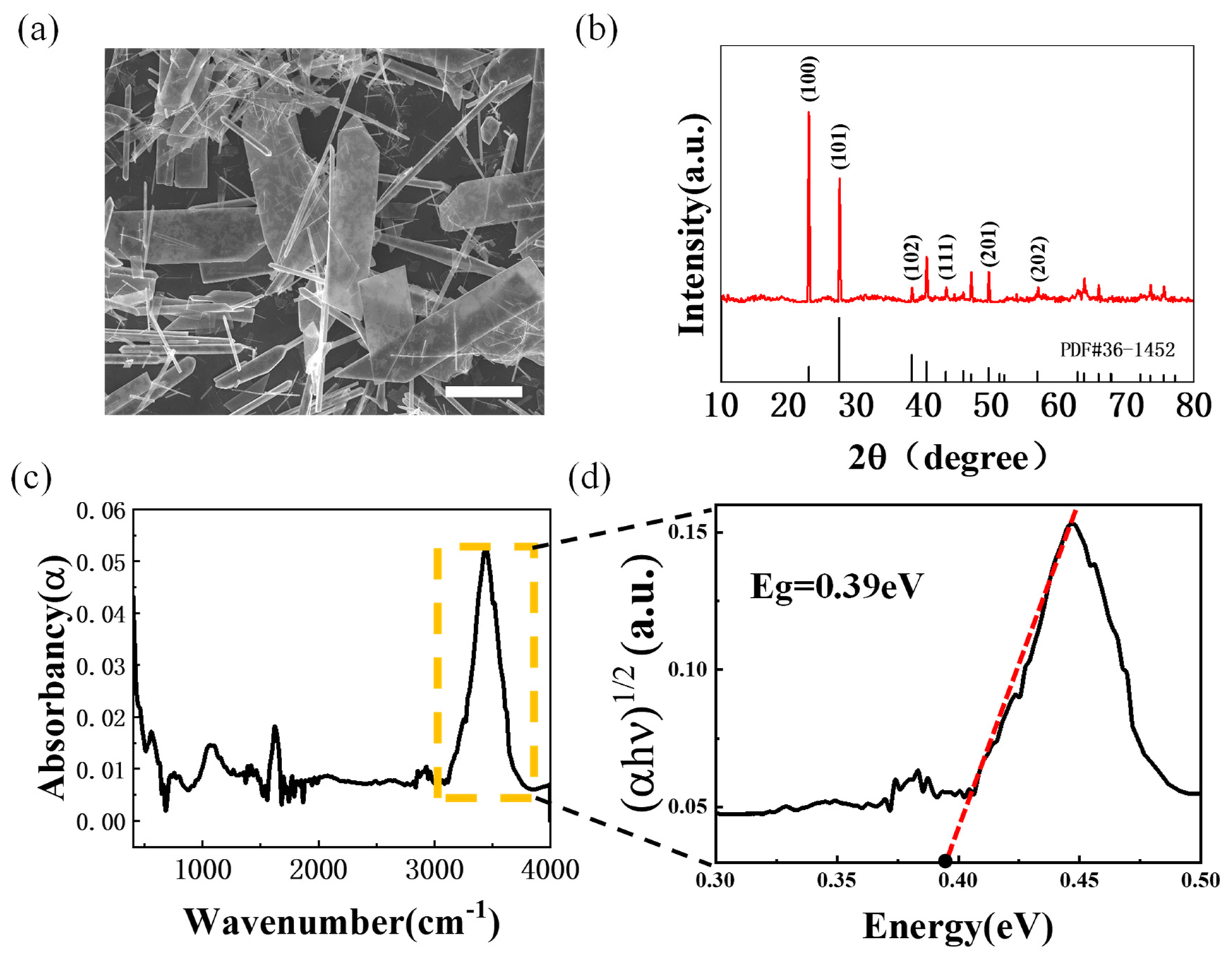
Figure 2.
(a) Schematic diagram of the surface of tellurium crystal flake treated with HP. (b) optical images of tellurium crystal flake successively treated with HP, with scale bar of 5um, the processing power and duration are marked accordingly. (c) Raman spectra of successive HP irradiation treated tellurium crystal flake.
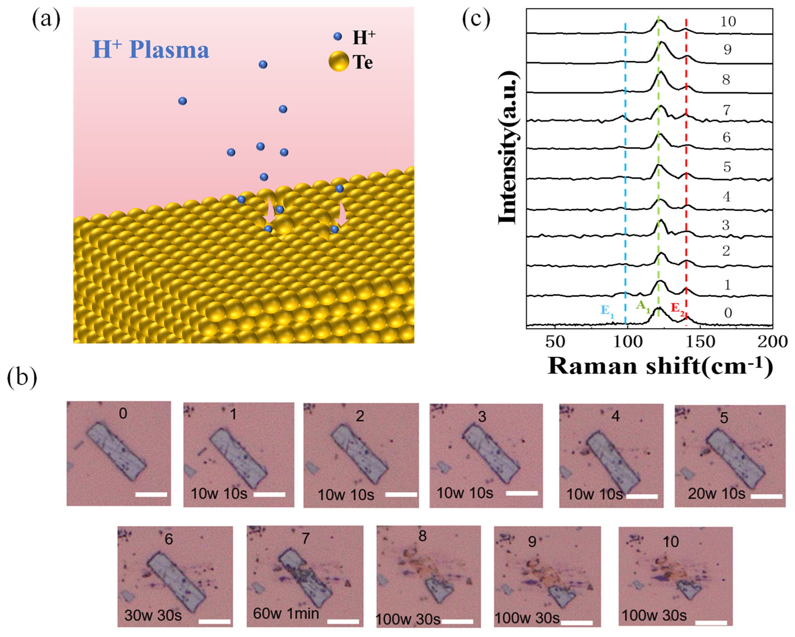
Figure 3.
CAFM contact mode probed IV curves of the tellurium flake with HP treatment for stage-1(a), and stage-2 (b); (c) CAFM contact mode probed IV curves of the tellurium flake under AP treatment. (d) The evolution diagram of tellurium conductance with HP and AP irradiation treatment.
Figure 3.
CAFM contact mode probed IV curves of the tellurium flake with HP treatment for stage-1(a), and stage-2 (b); (c) CAFM contact mode probed IV curves of the tellurium flake under AP treatment. (d) The evolution diagram of tellurium conductance with HP and AP irradiation treatment.
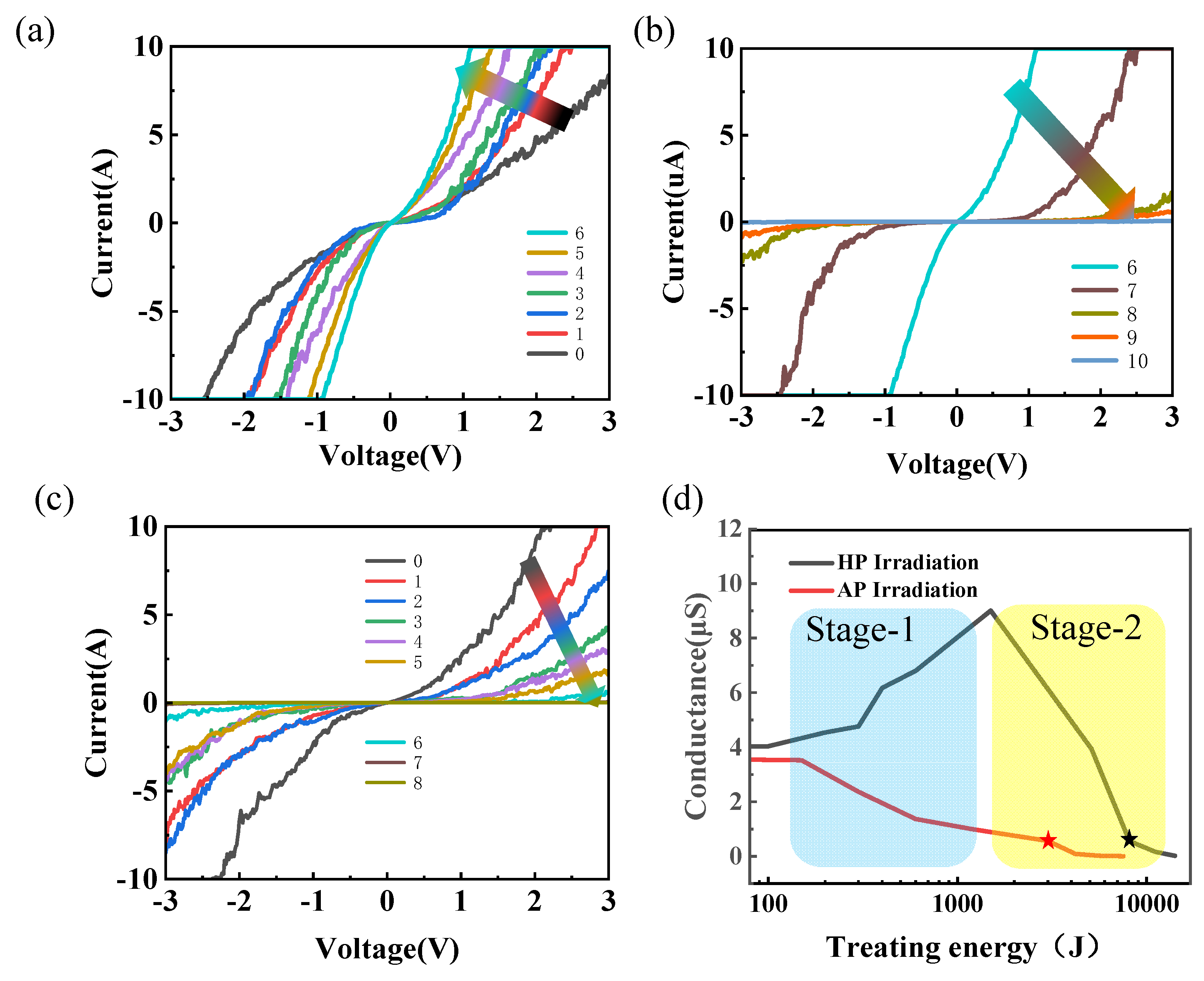
Figure 4.
the STS spectra for the HP and AP irradiation treated tellurium flake(a) HP irradiation treatment and (b) AP irradiation treatment (the distance between the dashed curves in each of the figure schematically shows the approximate trend of the band gap evolution).
Figure 4.
the STS spectra for the HP and AP irradiation treated tellurium flake(a) HP irradiation treatment and (b) AP irradiation treatment (the distance between the dashed curves in each of the figure schematically shows the approximate trend of the band gap evolution).
Disclaimer/Publisher’s Note: The statements, opinions and data contained in all publications are solely those of the individual author(s) and contributor(s) and not of MDPI and/or the editor(s). MDPI and/or the editor(s) disclaim responsibility for any injury to people or property resulting from any ideas, methods, instructions or products referred to in the content. |
© 2024 by the authors. Licensee MDPI, Basel, Switzerland. This article is an open access article distributed under the terms and conditions of the Creative Commons Attribution (CC BY) license (http://creativecommons.org/licenses/by/4.0/).
Copyright: This open access article is published under a Creative Commons CC BY 4.0 license, which permit the free download, distribution, and reuse, provided that the author and preprint are cited in any reuse.


