
Submitted:
09 January 2025
Posted:
10 January 2025
You are already at the latest version
Abstract
In the present work, a study of the structural defects in HfO2 thin films deposited by dip-coating on p-type silicon substrates treated under different conditions, such as air-annealing, ultraviolet irradiation, and simultaneous annealing-UV irradiation, is presented. HfO2 thin films were analyzed by grazing incidence X-ray diffraction, Raman spectroscopy, optical fluorescence, atomic force microscopy, and UV-Vis diffuse reflectance. Films treated at 200 ºC and 350 ºC present peaks corresponding to monoclinic HfO2. After UV treatment, films became amorphous. The combination of annealing at 350 ºC with UV treatment does not lead to crystalline peaks, suggesting that the UV treatment causes extensive structural damage. Fluorescence spectroscopy and UV-Vis spectroscopy suggested that films present oxygen vacancies as the main structural defects. A reduction of oxygen vacancies after a second thermal treatment was observed, but in counterpart, after UV irradiation, fluorescence spectroscopy indicates that more defects are created within the mobility gap, irrespectively of the simultaneous annealing at 350 ºC. An electronic band diagram was proposed assigning the observed fluorescence bands and optical transitions. The results suggest that the electronic structure of HfO2 films can be tailored with a careful choice of thermal annealing conditions along with the controlled creation of defects using UV irradiation, which would open the way to multiple applications of the materials either in microelectronics and photocatalytic/electrocatalytic applications such as photodegradation and hydrogen generation.
Keywords:
Hafnium oxide
; electronic structure
; oxygen vacancies
; thermal annealing
; UV irradiation.
1. Introduction
The improvement in the electrical performance of Thin Film Transistors (TFTs) has been subject of interest during the last decade. High-k dielectric materials such as hafnium oxide (HfO2) have been widely used as gate oxide for the fabrication of TFTs because of their low intrinsic leakage current [1,2]. However, structural and electronic defects in the gate oxide such as oxygen vacancies, dangling bonds or ionic impurities promote the creation of electronic traps with localized energy within its bandgap, which could promote an increased leakage gate current through this material, particularly on films prepared with low temperature processes, which are compatible with flexible substrates, for example [2]. On the other hand, the application of effective processing techniques at low temperatures, such as ultraviolet irradiation, plasma treatment, or conventional thermal treatments, have been widely used for improving the electronic performance of TFTs [3]. For example, the effect of temperature on the physical properties of HfO2 thin films deposited on silicon substrate has been analyzed [4,5], obtaining an increase in grain size, a reduction in surface roughness, organic residues, O-H bonds, and defect concentration with an increase in the applied temperature. E. Rauwel et al. [6] analyzed the effect of UV irradiation on HfO2 nanoparticles. According to the photoluminescence analysis, the emission band centered at 2.3 eV decreased with the application of UV light, which implies an increase in oxygen vacancies, which act as charge traps in the nanoparticles. Manoj Kumar et al. [7] presented the analysis of the physical properties of HfO2 thin films upon thermal treatment, and UV/ozone plasma treatment. The HfO2 films treated with UV/ozone plasma exhibited a reduction in impurities, because of a larger portion of Hf atoms is fully oxidized and the oxygen vacancies decreased. On the other hand, there is an increased interest in HfO2 in photocatalysis and electrocatalysis applications. For example, Mn-doped HfO2 nanoparticles [8] and HfO2-rGO composites [9,10] have been reported for methylene blue photodegradation and electrocatalytic H2 evolution, respectively. For this sake, the role of defect engineering has been demonstrated as a promising way to achieve better efficiency.
In the present work, the effect of UV and thermal post deposition treatments on the defect density in HfO2 films prepared by dip coating at room temperature was assessed by X-ray diffraction, Raman spectroscopy, atomic force microscopy, UV-Visible spectroscopy and fluorescence spectroscopy.
2. Materials and Methods
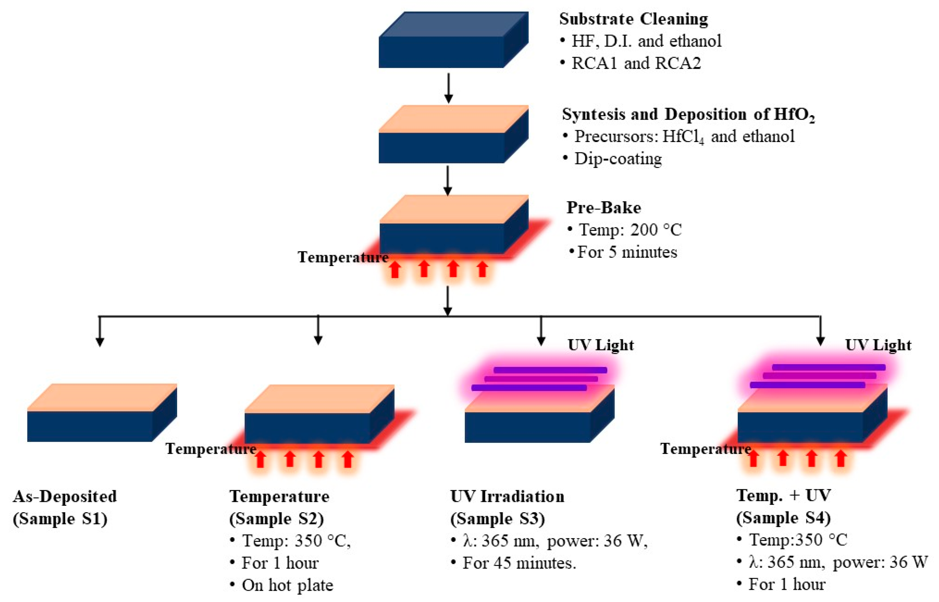
HfO2 thin films were deposited on (100) p-type silicon substrates (p-Si) by the dip-coating technique. First, substrates were cleaned by HF solution, deionized (DI) water and ethanol, and then by the RCA1 (5 DI H2O: 1 NH4OH: 1H2O2 at 70 ºC) and RCA2 (6 DI H2O: 1 HCl: 1 H2O2 at 70 ºC) processes. Thereafter, 5.16 grams of hafnium chloride (HfCl4, 99.99% Sigma-Aldrich) were dissolved into 40 mL of ethanol. Four samples were prepared by dipping the substrates into the prepared solution at room temperature for 30 min. After being removed from the bath, all the samples were baked in air for 5 min at 200 °C (sample S1). Afterwards, another sample was air-annealed at 350 °C by 1 hour (sample S2). Another sample was irradiated with a UV source of 340 nm and 36 W by 1 hour (sample S3). The later sample (sample 4) was simultaneously air-annealed at 350 °C during UV irradiation 1 hour. Figure 1 shows the flow diagram of the process, and the samples prepared.
Films were characterized by grazing incidence X-ray diffraction in a Siemens D5000 instrument, using Cu Kα radiation (0.15408 nm), at an incidence angle of 1º, a step size of 0.02º, and a step time of 3 s. Raman spectroscopy was performed in a Raman i-Plus spectrometer with a 532 nm laser with a nominal power of 36 mW, focused through a 20 X microscope objective. UV-Visible spectroscopy in the diffuse reflectance mode was performed in a Varian Cary 5000 Instrument using an integrating sphere. Optical fluorescence spectroscopy was done using an excitation wavelength of 270 nm in a Horiba-Jobin Yvon instrument. Atomic force microscopy was done in a TT AFM Workshop instrument in the intermittent contact mode, using a DLC-coated tip with a 190 µm cantilever with a resonance frequency of 190 kHz and a force constant of 48 N/m.
Figure 1.
Process flow diagram used for production of HfO2 samples.
3. Results
To determine the effect of the post-deposition treatments on the structural, optical, morphological and electronic characterization of the HfO2 films, this section presents the GIXRD, Raman, AFM, fluorescence, and UV-Vis reflectance data.
3.1. Structural Characterization
3.1.1. X-ray Diffraction
Figure 2 presents the grazing incidence X-ray diffractograms of the p-Si substrate and the S1-S4 samples, compared with the Powder Diffraction File PDF 36-0104 corresponding to the monoclinic phase of HfO2. The S1 and S2 films present diffraction peaks at 2 theta 29.24º, and 2 theta 29.24º and 32.62º, respectively, related with the (-111) and (111) reflections of monoclinic HfO2 [4,5]. The presence of the second peak of the (111) plane in the sample S2, annealed at 350 ºC indicates a higher crystallinity. The observed 2 theta shift of 1º of both peaks with respect to the reported PDF is related with the low X-ray incidence angle. S3 and S4 films do not present diffraction peaks apart from the Si substrate, indicating that the UV process led to amorphous films. Future work will explore the effect of film crystallinity varying both temperature and annealing time around the monoclinic phase dominion [4,5] and its effect on the film electronic properties.
3.1.2. Raman Spectroscopy
Figure 3 shows the Raman spectra of the four HfO2 samples and the p-Si as reference sample (P1). The monoclinic HfO2 structure has 18 optical phonon modes, which are (9Ag + 9Bg) for Raman active modes and (8Au +8Bu) for IR-active [8]. Figure 3 depicts optical vibration modes centered at 133 cm-1 (Ag mode), 301 cm-1 (Ag mode), 617 cm-1 (Bg mode), 671 cm-1 (Ag mode) and 821 cm-1 (Bg mode).
The most intense peak corresponds to the 301 cm-1 vibration related with Hf-Hf bonds, related with the formation of oxygen vacancies [5,9]. A defined peak at 133 cm-1 arises in the spectrum of S2 sample, consisting with the higher crystallinity of the sample. Nevertheless, there are only slight differences in the peak intensities between the films, therefore, not much information can be derived from the effect of post-deposition treatment on the local film structure.
3.2. Film Morphology by Atomic Force Microscopy
Figure 4 presents the 20 x 20 µm2 topographic images of the S1-S4 HfO2 thin films. Initially, the image of the S1 film shows a cracked surface with some spherical particles spread on the surface. The characteristic cracked morphology of the HfO2 films may be due to the type of deposition used, dip coating, where the solvent evaporation leads to the observed morphology, opposite to the film morphology achieved by sputtering [11]. Upon thermal annealing at 350 ºC, the size of the cracks decreases in the S2 film, indicating the films become more compact. When UV radiation is applied on the S3 film, a decrease in the width and the length of the cracks is observed, indicating coalescence of the films, possibly explained by a sequential bond rupture by the UV radiation, followed by “plastic” self-healing of the film which leads to the amorphization observed in the GIXRD [12]. However, in S4 film, where both treatments (thermal and UV radiation) are combined, a further increase of the shape and size of the cracks occurred, suggesting that the bond rupture is not followed by a recrystallization. Vargas et al. showed that increasing annealing temperature leads to increased film compacity [4], although there is not a study of increased annealing time at low temperature with to increase coalescence, which will be explored in future work.
In Figure 5, a) height distribution and b) roughness root mean square values obtained from the AFM images are presented.
As inferred from topographic images (Figure 4), in Figure 5a) the height distribution is almost constant in S1 and S2 with 0.64 and 0.66 µm respectively, decreasing the value of heights in S3 to 0.54 µm and the value increases in S4 until 0.61 µm, obtaining a value closer to S1. In Figure 5b), the RRMS shows a similar behavior; the RRMS has a value of 118 nm of roughness in S1, increasing in S2 to 146 nm, followed by a decrease in S3 to 95 nm and increasing again in S4 to 118 nm, returning to the value obtained in S1.
S1 and S4 present similar values in the distribution of heights and roughness, although S4 has been applied heat treatment and UV irradiation, according to the literature there should be an increase in the crystallinity of the HfO2 film [12], which would contribute to an improvement in its morphological properties, however, S4 shows values and properties similar to those presented in S1, which could be due to the longtime of heat treatment and irradiation, generating rupture of bonds in the structure of the film. In addition, it has correspondence with what was obtained in the X-ray diffraction analysis where it was found that S3 and S4 did not present additional peaks to those characteristics of Si, in other words, the analyzed material is amorphous.
In future work, optimal heat treatment and UV irradiation times will be assessed to tailor the film compacity/porosity, which could benefit the use as insulators in TFTs or in electrocatalytic applications, respectively.
3.3. Optolectronic Properties
3.3.1. Optical Fluorescence
Figure 6(a) presents the fluorescence spectra of S1-S4 samples, performed with an excitation wavelength of 270 nm. It can be observed that samples S1 and S2 present the lowest total fluorescence while S4 presents the highest, suggesting that this film has the highest defect density [13]. Emission maxima are evident at ca. 2.0 eV, 2.8 eV, 2.9 eV, 3.0 eV, and 3.8 eV. S1 and S2 spectra display less fluorescence features than S3 and S4. Figure 6(b)-(e) shows the deconvoluted emission spectra of the samples.
As shown in Figure 6(a), the intensity and position of the fluorescence bands differ upon the film treatment. To have a semiquantitative characterization, Figure 7 presents the analysis of the fluorescence peaks, where Figure 7 (a) shows the peaks observed in each spectrum after deconvolution and the corresponding peak positions, and Figure (b) displays the areas of the peaks, normalized with the total area under the fluorescence emission curve, as a measure of the relative density of the electronic states contributing to the emission.
As observed in Figure 7(a), samples S1 (treated at 200 ºC) and S2 (treated at 200 ºC and then at 350 ºC) display three emission peaks at ca. 2.5 eV, 2.8 eV and 3.8 eV. Correspondingly, samples S3 and S4 which have UV treatment display additional emission peaks at ca. 2 eV, 3 eV, and 3.5 eV. The peak at 2.8 eV presents an evident red shift from 2.82 eV (S1) to 2.71 eV (S4) while the position of the emission at 3.8 eV is almost invariant. These bands are congruent with those reported in [14]
The emission band at 2.5 eV has been related either to hydrogen or chlorine defects [15] and it is only present before UV treatment. The emission band at 2.8 eV is characteristic of oxygen vacancy defects in HfO2 [10], On the other hand, the bands at 2.0, 3.0 and 3.5 eV which appear only after the treatment with UV light may arise from dangling bonds and defect centers [1]. The increase of emission due to defects in S3 and S4 films is in correspondence with the XRD analysis where it was found that S3 and S4 are amorphous. The band at 3.8 eV may arise from direct recombination from shallow states within the gap to the valence band [16] but has been also attributed to the OH radical within the structure [14].
With respect to the relative contribution of each band to the fluorescence spectrum, Figure 7(b) presents the normalized areas of the fluorescence peaks. It can be observed that the dominant emissions in all the samples arise from the oxygen vacancies at 2.8 eV, although its relative intensity is variable with the sample treatment and the presence of additional emission bands upon UV treatment. For example, in S3, the 2.8 eV emission is lower than in S4, but the emissions at 3.0, 3.5 and 3.8 eV are higher in S3 than S4, indicating a reduction of the available states with the UV + annealing at 350 ºC. The band at ca. 2.5 eV related with hydrogen/chlorine defects, reduced its relative intensity with the increase of temperature from S1 to S2.
The results indicate that the electronic structure of the HfOx films is largely influenced by the UV treatment, which causes an increase in the defect states, which partially with the annealing temperature. More accurate defect engineering would be possible with optimized annealing temperature and time and UV irradiation times.
3.3.2. UV-Vis Spectroscopy
S1-S4 samples were analyzed by UV–Vis diffuse reflectance spectroscopy for a wavelength range of 200 to 800 nm. By applying the Kubelka-Munk function (FK-M) the optical absorption coefficient α, was estimated using:
where R is the diffuse reflectance.
〖α~F〗_(K-M) =(1-R)2/2R
To assess the electronic states near the absorption edge, the following expression as function of FK-M was used:
where A is a constant that does not depend on the photon energy, h is plank constant, ν is the frequency, Eg is the bandgap and n can take the values 0.5 or 2 depending if the band gap is direct or indirect [17]. The band gap for HfO2 has been reported as indirect at ca. 6 eV [4] and direct at ca. 5.8 eV [11]. Figure 8 shows the analysis of the optical reflectance of the S1-S4 samples. Figure 8(a) shows the reflectance spectra, Figure 8(b) the Tauc plot (F(R)hν)0.5 vs hν which corresponds to indirect transitions, and Figure 8(c) the Tauc plots (F(R)hν)2 vs hν corresponding to the direct transitions for the S1-S4 HfO2 samples, respectively [17].
hνα~hvF_(K-M)∝〖A(hν-Eg )n
The reflectivity of the films decreases from higher to lower wavelength, according to the reported refractive index vs wavelength [4]. From Figure 8(a) it can be observed that film S1 has the highest reflectivity vs wavelength behavior (%R from 5 to 80%). It has been reported that the refractive index increases with the temperature [4]. The other reflectance spectra have similar reflectivity values and features, also suggesting an increased density upon the post-deposition treatments [4]. Figure 8(b) shows the optical behavior of the films when the indirect transitions (F(R)hv1/2 vs energy plot) are assessed. In the plot the several linear regions are indicated with straight lines for each spectrum, indicating the presence of delocalized states within the band gap. It is evident the difference of such states from the S1 sample, with the samples with post deposition treatment. In Figure 8(c), the F(R)hv2 vs energy plot which accounts for direct transitions is shown. Several linear regions are indicated at around 5, 3.5-4.0, 2.6-3.0 and 2 eV. The spectrum of the S1 sample shows a defined transition at ca. 5.6 eV which can be assigned to the direct band gap of HfO2 [11], followed by another defined state at ca. 5 eV which nature is discussed below. Correspondingly, the spectra of samplesS2-S4 have similar features but the fundamental transition is not observed, possibly because the spectral range where the transmittance was assessed [4]. The areas within dotted circles indicate extended absorption tails around 5.0 eV, 3.8 eV and 2.8 eV respectively, related to disorder and widening of the density of available states around these energies within the mobility gap.
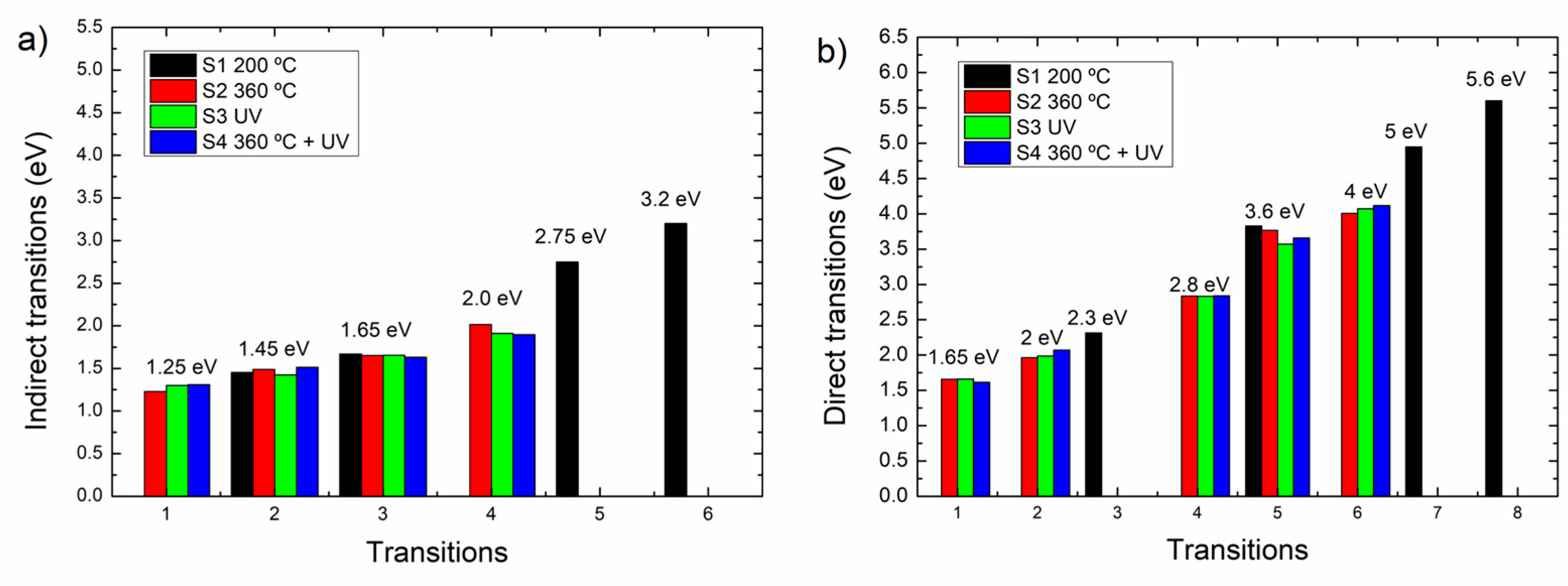
Following Ibrahim and Al-Ani [17], the intersections where y = 0 in the plot are not necessarily electronic transitions, but depending on the disorder degree, they can be rather considered as extrapolations from delocalized states to the zero of density states, according to the Davis-Mott model. Thus, in Figure 9 the energy values of the extrapolations at y = 0 of the indirect and direct related transitions are shown. In Figure 9(a) corresponding to F(R)hv1/2 = 0 states the sample S1 presents y=0 at 1.45 eV, 1.65 eV, 2.75 eV and 3.2 eV, while samples S2-S4 display states at 1.25 eV, 1.45 eV, 1.65 eV and 2.0 eV. Correspondingly, the F(R)hv2 = 0 plots have several states; sample S1 has y=0 at 2.3 eV, 3.6 eV, 5.0 eV and the fundamental band gap at 5.6 eV and the samples S2-S4 at 1.65 eV, 2.0 eV, 2.8 eV, 3.6 eV and 4 eV.
4. Discussion
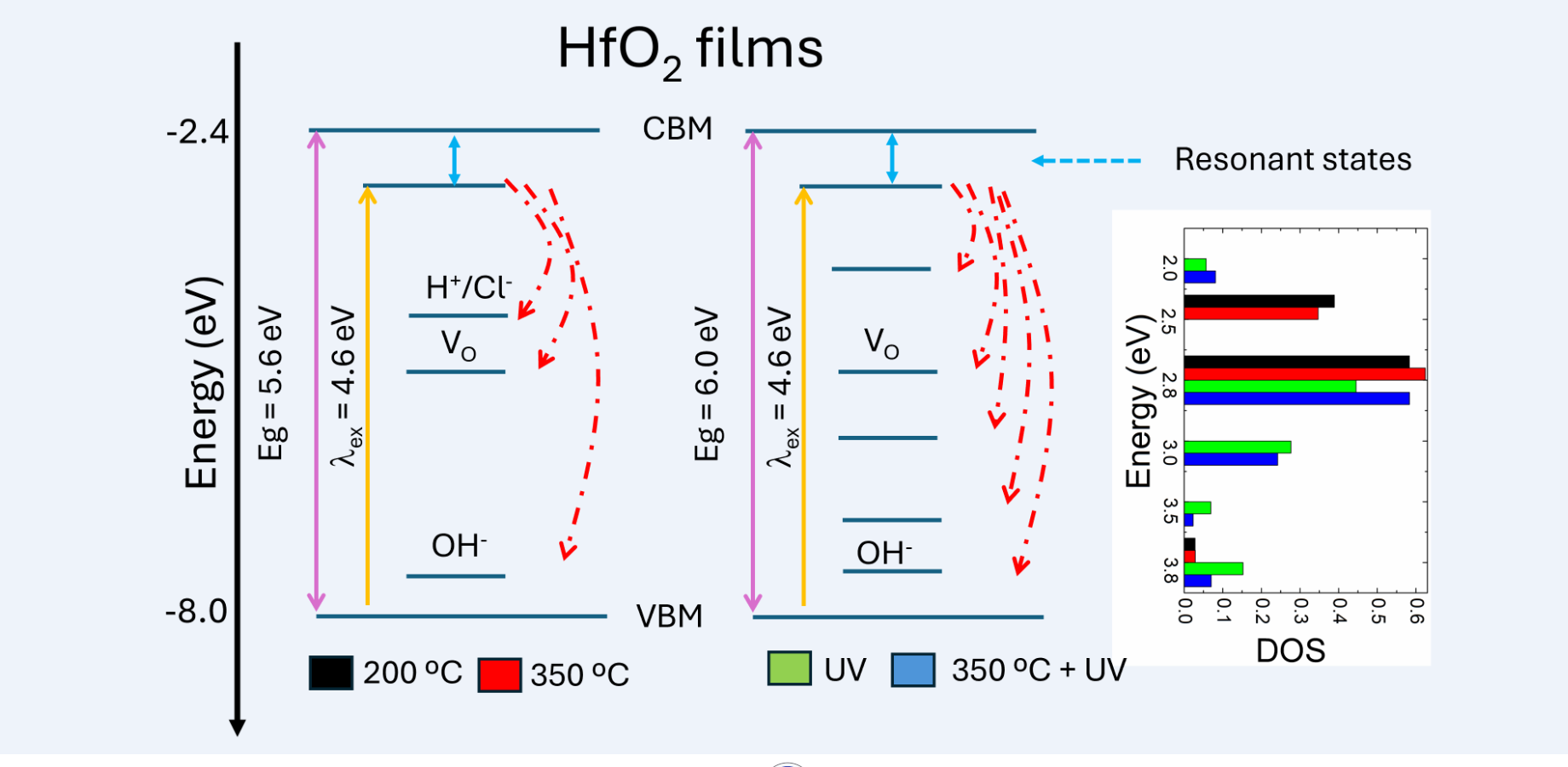
Figure 10 summarizes the results from the fluorescence and UV-visible spectroscopy, with two electronic band diagrams. Figure 10(a) presents the electronic band diagrams from the fluorescence data for the samples S1-S2 (left) and samples S3-S4 (right). The positions of the conduction band and valence band edges were calculated from González et al. data [8]. The level below the conduction band corresponds to empty levels where electrons arrive upon 270 nm excitation to then produce radiative decay. This level has been observed by several authors [16,18,19,20,21] and it has been attributed either to defect states related to the observed Urbach tail below the band gap in polycrystalline HfO2 [18], as well as to resonant states originating from the presence of localized Hf 5 d polaron states at the Fermi level, which in turn, push the un-occupied states 2 eV above the Fermi level [20,21] These polaron states arise from the oxygen vacancies indicated by the fluorescence band at 2.8 eV [16,19,20,21]. The levels within the mobility gap were assigned considering the observed fluorescence bands. As described in section 3.3.1., in S1 and S2 samples, the observed fluorescence peaks are associated with H+/Cl- states [15], oxygen vacancies, and OH-states [14] respectively. Upon UV treatment, the peak associated with oxygen vacancies reduced but novel peaks were observed. Also, the H+ states are not observed in samples S2 and S4 and there is an increase in the fluorescence intensity OH states, in contradiction with the results from Kim et al [12] who reported that UV + rapid thermal annealing at 450 ºC lead to a reduction in OH states, which confirms the possibility of tailoring the defect states with a careful election of UV and thermal treatment conditions. From the above diagram is possible to states that the normalized intensity of the fluorescence peaks is then, a measure of the density of the electronic states within the mobility gap as shown in the right side of Figure 10(a).
Figure 10(b) shows the electronic band diagram for the S1 (left) and S2-S4 samples (right) from the point of view of the direct electronic transitions within the mobility gap calculated from the F(R)hv2 = 0 plot [16]. In this diagram the depicted transitions were assigned considering the fluorescence bands and the discussed assignation to different electronic states. For the case of the S1 sample, the direct band gap was directly obtained from the F(R)hv2 = 0 plot as well as the transition at 5 eV, which was already assigned to the resonant states below the band gap [20,21]. The transitions at 3.6 eV and 2.3 eV arise from the occupied oxygen vacancy levels to the conduction band and from the valence band to unoccupied H+ states, respectively. The oxygen vacancy levels, and H+ levels are very close (ca. 03 eV) which may lead to thermalization thus explaining the high DOS for the H+ level. For samples S2-S4, the fundamental VB-CB transition was not observed, due to an increase of Eg of these samples, but as samples present fluorescence upon excitation at 270 nm, the resonant states were kept in the diagram and Eg was set at 6 eV. Thus, the transition from the oxygen vacancy level to the CB is still observed at 3.6 eV and a new 4 eV transition arises from the novel states, which may arise from Hf 5d up and down and O2 p up and down levels [21]. This new state is 2 eV above the valence band maximum, which is of interest for photocatalytic applications [8]. The blue dotted circles in Figure 10(b) indicate the presence of extended absorption tails, which explain the variations of the transition values as observed in Figure 9. With respect to the indirect transitions, any of them showed a sharp onset, which is consistent with the Davies-Mott model for amorphous semiconductors [17].
Figure 10.
Electronic band diagram of the S1-S4 films considering (a) fluorescence data and (b) (F(R)hν)2 = 0 transitions from the UV-visible spectra.
Figure 10.
Electronic band diagram of the S1-S4 films considering (a) fluorescence data and (b) (F(R)hν)2 = 0 transitions from the UV-visible spectra.
As a final consideration, the results suggest that additionally to doping [8] or preparing heterostructures [9,10] it is possible to tailor the electronic structure of HfO2 using an adequate selection of thermal and UV treatment for photocatalytic/electrocatalytic applications. Also, the present study shed more light on the defects that control the performance of HfO2 as high-k dielectric in microelectronics.
5. Conclusions
In the present work HfO2 films prepared by room temperature dip coating were treated at different conditions after deposition onto p-Si. Films were characterized by XRD, Raman, AFM, UV-Vis and fluorescence spectroscopy. Films are monoclinic after a thermal treatment of 350 ºC and became amorphous and less compact upon UV treatment. A band diagram which considered both optical and fluorescence spectroscopy was proposed including the normalized fluorescence as a measure of the Density of States. The results indicate that the UV treatment generates several defect states within the mobility gap which may decrease the performance of HfO2 films in microelectronics but that may allow its use in photocatalytic/electrocatalytic applications.
Author Contributions
Conceptualization, F. L.-H. and F. C.-B.; methodology, S.S.-R., and F.I.G.-M.; validation, R.M.W.-G., A.L.M.-R. and F.L.-H.; formal analysis, F.C.-B; investigation, S.S.-R., and F.I.G.-M.; resources, A.L.M.-R.; data curation, R.M. W.-G., A.L.H.-M.; writing—original draft preparation, S.S.-R.; F.I.G.M., R.M. W.-G., F.L.-H., F.C.-B. writing—review and editing, F.I.G.-M., F.C.-B.; visualization, F.I.G.-M., F.C.-B.; supervision, R.M.W.-G., A.L.M.-R. and F.L.-H.; project administration, F.L.-H.; funding acquisition, F.L.-H. All authors have read and agreed to the published version of the manuscript.
Funding
This research was funded by CONAHCYT grant number 2019-40798. The APC was waived by MDPI.
Data Availability Statement
Data is available upon reasonable request.
Acknowledgments
GIXRD analyses were carried out at the National Laboratory of Nano and Biomaterials, CINVESTAV-IPN; financed by the FOMIX-Yucatán grant numbers 2008-108160, CONACYT LAB-2009-01-123913, 292692, 294643, 188345 and 204822. We thank Dr. Patricia Quintana for the access to LANNBIO and to M.Sc. Daniel Aguilar for obtaining the diffractograms. Partial funding from CONAHCYT 2019-40798 and 2022-321595 projects for AFM and Raman spectroscopy measurements is granted.
Conflicts of Interest
The authors declare no conflicts of interest. The funders had no role in the design of the study; in the collection, analyses, or interpretation of data; in the writing of the manuscript; or in the decision to publish the results.
References
- Seonghwan Hong, Sung Pyo Park, Yeong-gyu Kim, Byung Ha Kang, Jae Won Na & Hyun Jae Kim, Low-temperature fabrication of an HfO2 passivation layer for amorphous indium–gallium–zinc oxide thin film transistors using a solution process, Scientific Reports 7 (2017) 16265. [CrossRef]
- Young Bum Yoo, Jee Ho Park, Kuen Ho Lee, Hyun Woo Lee, Kie Moon Song, Se Jong Leec, and Hong Koo Baik, Solution-processed high-k HfO2 gate dielectric processed under softening temperature of polymer substrates, J. Mater. Chem. C, 2013,1, 1651-1658. [CrossRef]
- Won Kim, Jung-Hwan Bang, Hyun-Seok Uhm, Sang-Hyuk Lee, Jin-Seok Park, Effects of post plasma treatment on material properties and device characteristics in indium zinc oxide thin film transistors, Thin Solid Films 519 (2010) 1573–1577. [CrossRef]
- M. Vargas, N.R. Murphy, C.V. Ramana, Structure and optical properties of nanocrystalline hafnium oxide thin films, Optical Materials, 37 (2014) 621-628. [CrossRef]
- Tingting Tan, Zhengtang Liu, Hongcheng Lu, Wenting Liu, Hao Tian, Structure and optical properties of HfO2 thin films on silicon after rapid thermal annealing, Optical Materials 32, (2010) 432-435. [CrossRef]
- E Rauwel, A Galeckas and P Rauwel, Photoluminescent cubic and monoclinic HfO2 nanoparticles: effects of temperature and ambient, Mater. Res. Express 1 (2014) 1 015035. [CrossRef]
- 2017; 7. Manoj Kumar, Hakyung Jeong, Dongjin Lee, Effect of UV/ozone plasma treatment on sol–gel-derived HfO2 thin films, Ceramics International 43 (2017) 1174–1179, Ceramics International 43 (2017) 1174–1179.
- Luis A. González, Saúl Gálvez-Barboza, Efrain Vento-Lujano, José L. Rodríguez-Galicia, Luis A. García-Cerda, Mn-modified HfO 2 nanoparticles with enhanced photocatalytic activity, Ceramics International 46 (2020) 13466–13473, Ceramics International 46 (2020) 13466–13473.
- Jayaraman, V.; Mahalingam, S.; Chinnathambi, S.; Pandian, G.N.; Prakasarao, A.; Ganesan, S.; Ramasamy, J.; Ayyaru, S.; Ahn, Y.-H. Facile Synthesis of Hafnium Oxide Nanoparticle Decorated on Graphene Nanosheet and Its Photocatalytic Degradation of Organic Pollutants under UV-Light Irradiation. Appl. Sci. 2022, 12, 11222. [CrossRef]
- Arokia Anto Jeffery, Sourabh S. Chougule, Imran Hasan, Jagadeesh Kumar Alagarasan, Parkavi Ravi Sankar, Prathap Somu, Mei-Ching Lin, Keerthika Kumarasamy, Young-Ho Ahn, Jayavel Murugasamy, Oxygen-Vacancy-Rich HfO2–x Nanoparticles Supported on Reduced Graphene Oxide for Electrocatalytic Hydrogen Evolution Reactions, ACS Appl. Nano Mater. 2023, 6, 24, 23053–23063. [CrossRef]
- J. de J. Araiza, L. Álvarez-Fraga, R. Gago, O. Sánchez, Surface morphology and optical properties of hafnium oxide thin films produced by magnetron sputtering, Materials 16 (2023) 5331. [CrossRef]
- Jaemin Kim, Jinsu Park, Duy Phong Pham, Myung Soo Yeo, HwaSung Rhee, Youg-Sang Kim, Eun-Chel Cho, Junsin Yi,Combination of ultraviolet exposure and thermal post-treatment to obtain high quality HfO2 thin films, Ceramics Internationa l47(2021) 9643–9650. [CrossRef]
- Candy Mercado, Zachary Seeley, Amit Bandyopadhyay, Susmita Bose, and Jeanne L. McHale, Photoluminescence of Dense Nanocrystalline Titanium Dioxide Thin Films: Effect of Doping and Thickness and Relation to Gas Sensing, ACS Appl. Mater. Interfaces 2011, 3, 7, 2281–2288. [CrossRef]
- Mingdong Kong, Bincheng Li, Chun Guo, Peng Zeng, Ming Wei and Wenyan He, he Optical Absorption and Photoluminescence Characteristics of Evaporated and IAD HfO2 Thin Films, Coatings 2019, 9, 307;. [CrossRef]
- Jaan Aarik, Hugo Mandar, Marco Kirm, Lembit Pung, Optical characterization of HfO 2 thin films grown by atomic layer deposition. Thin Solid Films 466 (2004) 41 – 47. [CrossRef]
- Papernov, S.; Brunsman, M.D.; Oliver, J.B.; Hoffman, B.N.; Kozlov, A.A.; Demos, S.G.; Shvydky, A.; Cavalcante, F.H.M.; Yang, L.; Demoni, C.S.; et al. Optical properties of oxygen vacancies in HfO2 thin films studied by absorption and luminescence spectroscopy. Opt. Express 2018, 26, 17608–17623. [CrossRef]
- Ibrahim, S. K. J. Al-Ani, Models of optical absorption in amorphous semiconductors at the absorption edge -a revie w and re-evaluation, Czechoslovak Journal of Physics, 44 (1994), 785-797. [CrossRef]
- N. V. Nguyen, Albert V. Davydov, Deane Chandler-Horowitz, and Martin M. Frank, Sub-bandgap defect states in polycrystalline hafnium oxide and their suppression by admixture of silicon, Appl. Phys. Lett. 87, 192903 (2005);. [CrossRef]
- M. C. Cisneros-Morales and C. R. Aita, The effect of nanocrystallite size in monoclinic HfO2 films on lattice expansion and near-edge optical absorption, Applied Physics Letters 96, (2010) 191904. [CrossRef]
- T. V. Perevalov, V. Sh. Aliev, V. A. Gritsenko, A. A. Saraev, V. V. Kaichev, E. V. Ivanova, and M. V. Zamoryanskaya, The origin of 2.7 eV luminescence and 5.2 eV excitation band in hafnium oxide, Applied Physics Letters 104, 071904 (2014);. [CrossRef]
- Zhongrui Wang, HongYu Yu & Haibin Su, The transport properties of oxygen vacancy-related polaron-like bound state in HfO x, Scientific Reports 3 (2013) 3246. [CrossRef]
Figure 2.
Grazing incidence X-ray diffractograms of the p-Si substrate, and the S1-S4 HfO2 samples compared with the monoclinic powder diffraction file, PDF 36-0104.
Figure 2.
Grazing incidence X-ray diffractograms of the p-Si substrate, and the S1-S4 HfO2 samples compared with the monoclinic powder diffraction file, PDF 36-0104.

Figure 3.
Raman spectra of HfO2 samples S1-S4 and p-Si substrate. Raman were acquired with a 532 nm laser.
Figure 3.
Raman spectra of HfO2 samples S1-S4 and p-Si substrate. Raman were acquired with a 532 nm laser.
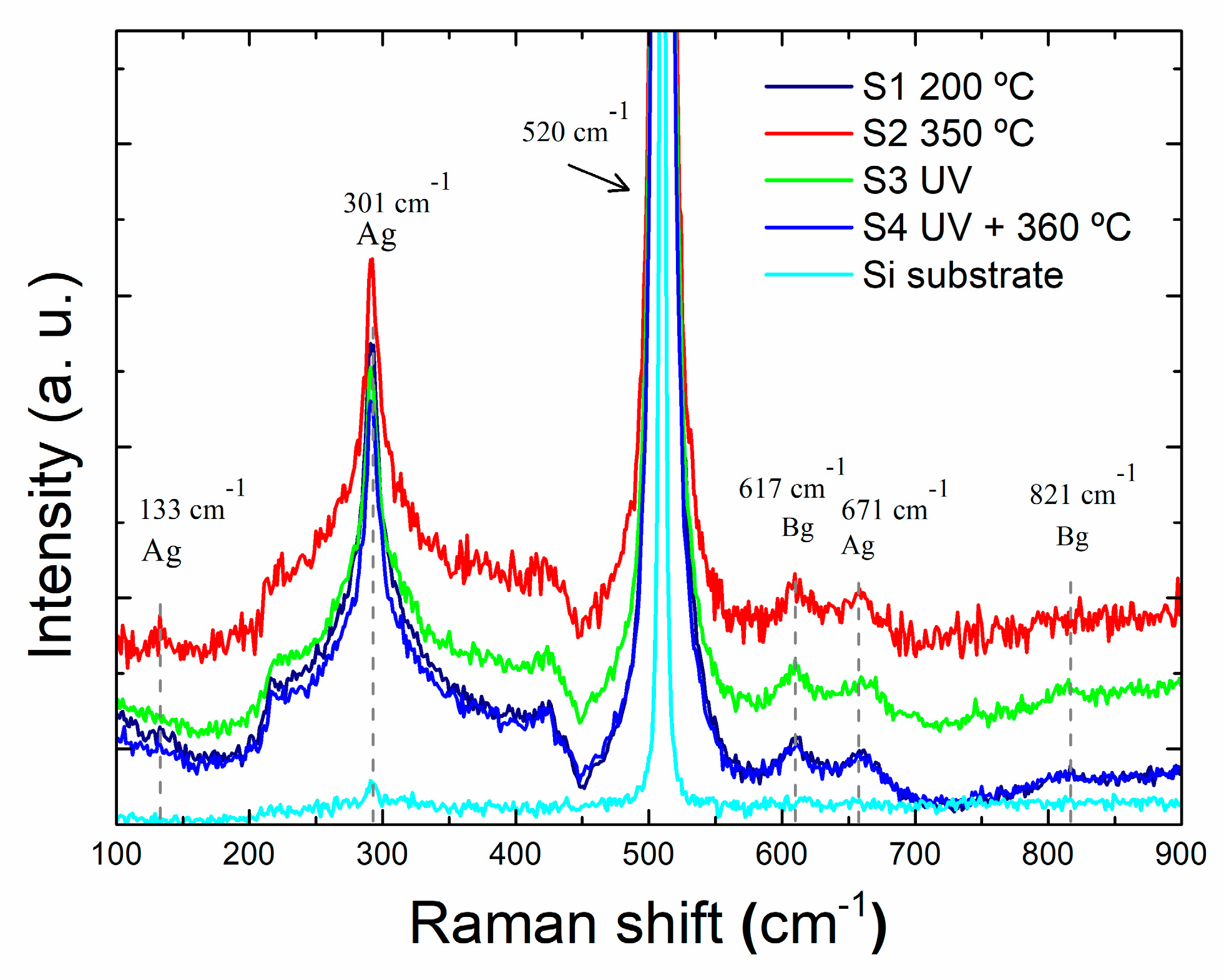
Figure 4.
20 x 20 µm2 AFM topographic images of the S1-S4 HfO2 thin films.
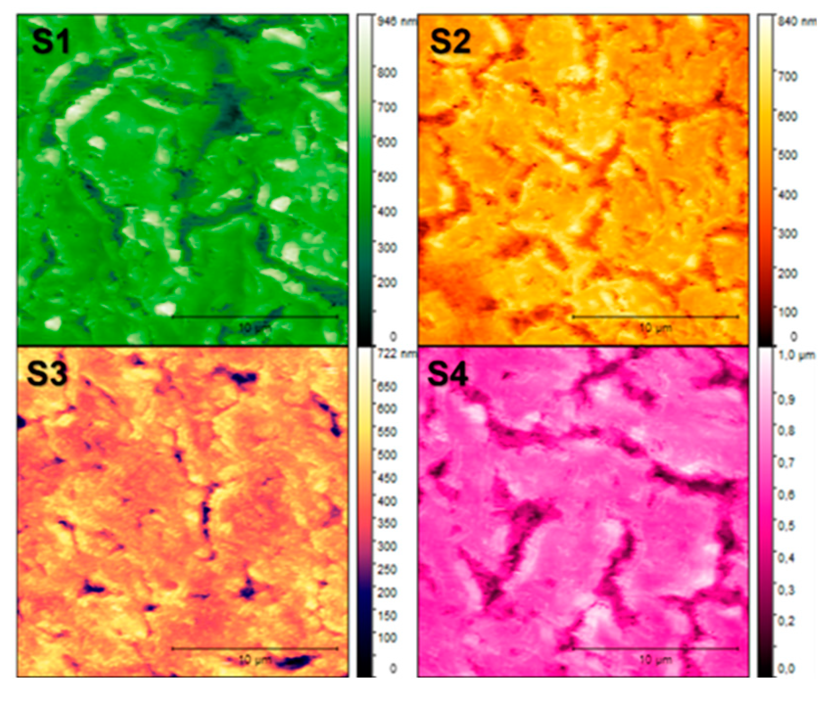
Figure 5.
a) Height distribution graph and b) roughness root mean square (RRMS) of HfO2 thin films.
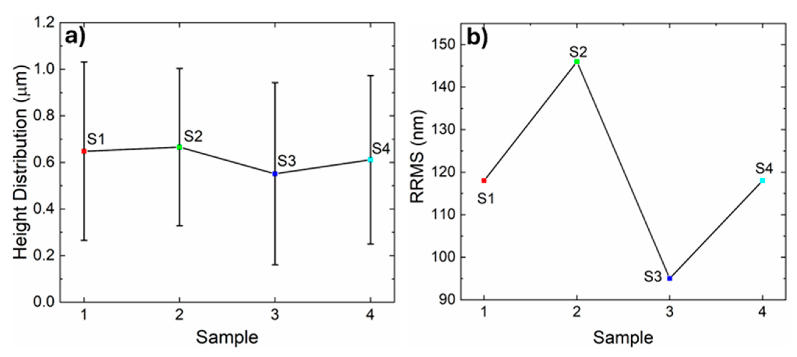
Figure 6.
Fluorescence spectra of (a) all the samples; (b)-(e) deconvoluted fluorescence spectra of (b) S1, (c) S2, (d) S3, and (e) S4.
Figure 6.
Fluorescence spectra of (a) all the samples; (b)-(e) deconvoluted fluorescence spectra of (b) S1, (c) S2, (d) S3, and (e) S4.
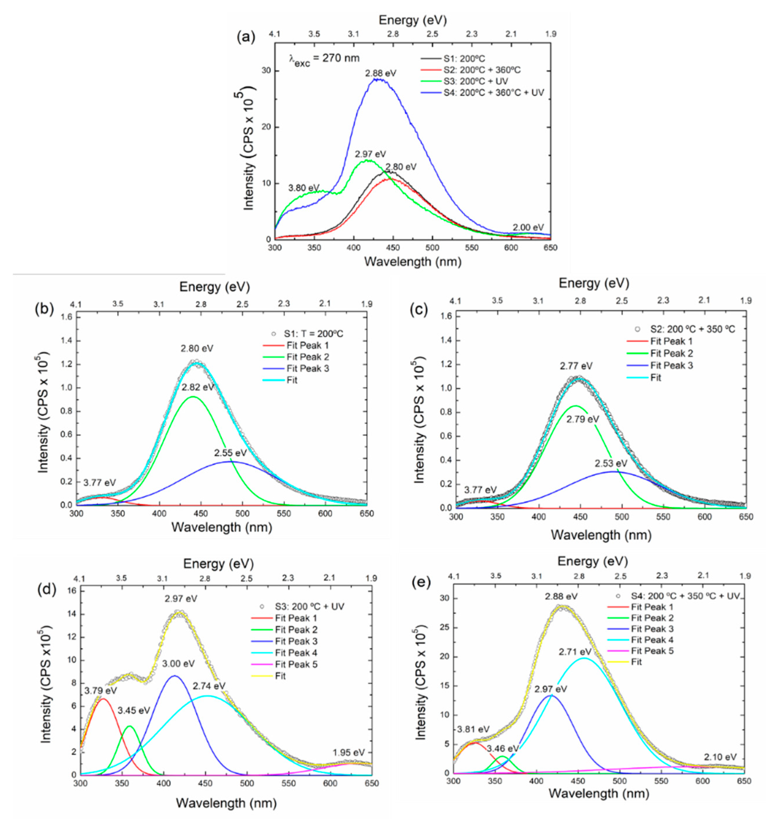
Figure 7.
(a) position of the fluorescence peaks and (b) normalized intensity with respect to the total fluorescence area of the fluorescence peaks of samples S1-S4.
Figure 7.
(a) position of the fluorescence peaks and (b) normalized intensity with respect to the total fluorescence area of the fluorescence peaks of samples S1-S4.
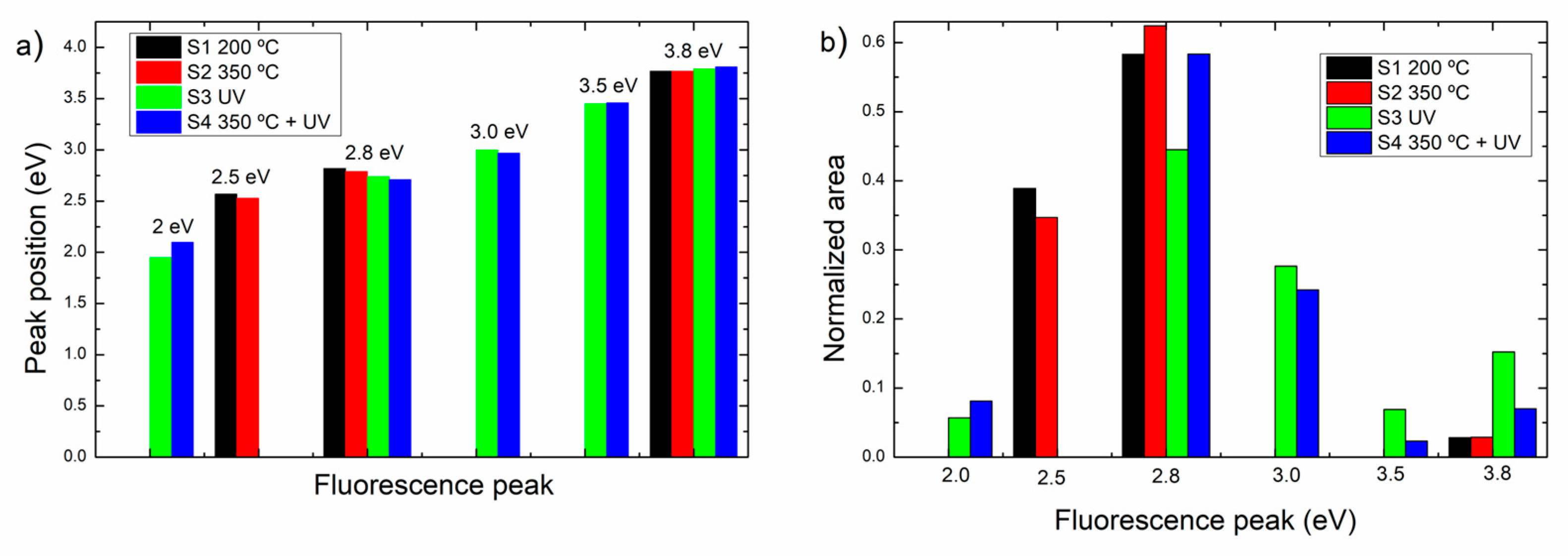
Figure 8.
(a) diffuse reflectance; Tauc plots (b) (F(R)hν)1/2 vs hν, and (c) (F(R)hν)2 vs hν of samples S1-S4.
Figure 8.
(a) diffuse reflectance; Tauc plots (b) (F(R)hν)1/2 vs hν, and (c) (F(R)hν)2 vs hν of samples S1-S4.
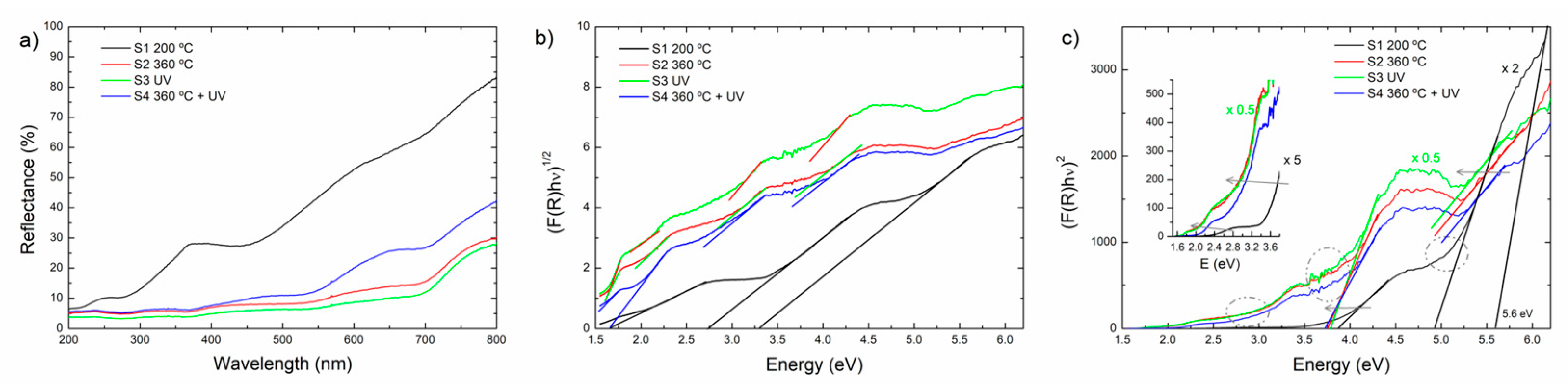
Figure 9.
(a) Allowed indirect transitions from the (F(R)hν)1/2 vs hν plot, and (b) Allowed direct transitions from the (F(R)hν)2 vs hν plot, of samples S1-S4.
Figure 9.
(a) Allowed indirect transitions from the (F(R)hν)1/2 vs hν plot, and (b) Allowed direct transitions from the (F(R)hν)2 vs hν plot, of samples S1-S4.
Disclaimer/Publisher’s Note: The statements, opinions and data contained in all publications are solely those of the individual author(s) and contributor(s) and not of MDPI and/or the editor(s). MDPI and/or the editor(s) disclaim responsibility for any injury to people or property resulting from any ideas, methods, instructions or products referred to in the content. |
© 2025 by the authors. Licensee MDPI, Basel, Switzerland. This article is an open access article distributed under the terms and conditions of the Creative Commons Attribution (CC BY) license (http://creativecommons.org/licenses/by/4.0/).
Copyright: This open access article is published under a Creative Commons CC BY 4.0 license, which permit the free download, distribution, and reuse, provided that the author and preprint are cited in any reuse.


