
Submitted:
05 January 2024
Posted:
05 January 2024
You are already at the latest version
Abstract
In the pursuit of energy-efficient spiking neural network (SNN) hardware, synaptic devices lev-eraging emerging memory technologies hold significant promise. This study investigates the ap-plication of the recently proposed HfO2/SiO2-based interface dipole modulation (IDM) memory for synaptic spike timing-dependent plasticity (STDP) learning. Firstly, through pulse measure-ments of IDM metal-oxide-semiconductor (MOS) capacitors, we demonstrate that IDM exhibits an inherently nonlinear and near-symmetric response. Secondly, we discuss the drain current re-sponse of a field-effect transistor (FET) incorporating a multi-stack IDM structure, revealing its nonlinear and asymmetric pulse response, and suggest that the degree of the asymmetry depends on the modulation current ratio. Thirdly, to emulate synaptic STDP behavior, we implement dou-ble-pulse-controlled drain current modulation of IDMFET using a simple bipolar rectangular pulse. Additionally, we propose a double-pulse-controlled synaptic depression that is valuable for optimizing STDP-based unsupervised learning. Integrating the pulse response characteristics of IDMFETs into a two-layer SNN system for synaptic weight updates, we assess training and classification performance on handwritten digits. Our results demonstrate that ID-MFET-based synaptic devices can achieve classification accuracy comparable to previously re-ported simulation-based results.
Keywords:
MOSFET
; Gate dielectrics
; Interface dipole
; Neuromorphic
; Spiking neural network
1. Introduction
Research on solid/solid interfaces is intricately connected to the evolution of semiconductor devices. Throughout the extensive history of semiconductor devices, substantial progress has been made in understanding the various interfaces that constitute these devices, such as metal/semiconductor, semiconductor/semiconductor, and oxide/semiconductor interfaces. In the development of MOSFETs, the fundamental building blocks of Si large integrated circuits, the interfacial electronic states, especially at the oxide/Si interface in the gate stack structure, are crucial elements influencing device operation and performance. Historically, the discovery of high-quality SiO2/Si interfaces formed by the thermal oxidation of silicon substrates around 1960 paved the way for the mass production manufacturing of CMOS integrated circuits [1,2]. In the 2000s, research institutions worldwide actively pursued the development of high-k gate dielectrics, accumulating knowledge about gate stacks containing various metal oxides [3,4]. The adoption of HfO2-based dielectrics in current state-of-the-art MOSFETs is a technological fruition of these research and development efforts [5]. In the 2010s, research on non-volatile memories based on MOSFETs incorporating high-k dielectrics experienced a significant surge [6,7]. Ferroelectric field-effect transistor (FeFET) memory, integrating ferroelectric materials into the gate stack, and conventional flash memory with high-k dielectrics garnered considerable attention [8,9]. The discovery of ferroelectric HfO2 in 2021 captured researchers' interest due to its excellent material compatibility with silicon semiconductor technology [10], driving continued active research and development for memory applications [11,12,13,14]. A notable recent research trend in FeFETs, similar to the purpose of this study, is the development of analog memories for neuromorphic applications [15,16].
Research on dipole layers induced at dielectric/dielectric interfaces has primarily advanced for the purpose of controlling the threshold voltage of high-k MOSFETs [17,18]. It has been reported that a small dipole layer is formed at the HfO2/SiO2 interface used in this study [19,20]. Interfacial dipole modulation (IDM) memory was conceived based on the studies of such high-k gate stack structures, with the objective of inducing MOS threshold voltage shifts similar to FeFETs. The first reported IDM results were observed in a HfO2/SiO2 stack structure incorporating a 1 monolayer (ML) of TiO2, as depicted in Figure 1a [21]. A MOS capacitor with such a stack structure exhibits high-frequency C-V curve with small hysteresis, illustrated in Figure 1b. This phenomenon was elucidated by the alteration in the bonding state around the Ti atoms at the SiO2/HfO2 interface, causing a change in the potential difference (interfacial dipole) between SiO2 and HfO2. Subsequently, hard x-ray photoelectron spectroscopy studies of IDMMOS and IDM metal-insulator-metal structures have revealed changes in Ti oxidation states synchronized with memory operation, supporting the notion that the origin of IDM is the structural change around the interfacial Ti atoms [22,23]. As IDM operates at amorphous dielectric/dielectric interfaces, it does not necessitate high-temperature crystallization annealing, in contrast to ferroelectric HfO2, and has been verified even with low-temperature annealing at around 300°C [24]. Furthermore, as shown in Figure 1c, the modulation operation exhibits a gradual change with respect to the applied voltage. This feature is also thought to originate from atomic-scale disorder at the amorphous dielectric/dielectric interface. The gradual threshold change is anticipated to be beneficial for analog operation in synaptic devices, as discussed later. On the other hand, the modulation range of HfO2/SiO2-based IDM is relatively small, up to about 0.33 V [21,24]. To extend the modulation range, a multilayered HfO2/SiO2 structure has been proposed. For example, an FET incorporating a multilayered IDM with six TiO2 modulation layers achieves a threshold voltage shift of over 1 V and a current change of over six orders of magnitude [21]. The pulse response characteristics of IDMFETs have been investigated, demonstrating stable and repetitive modulation. The authors believe that these characteristics make it suitable for use as a synaptic device in spiking neural networks and have conducted detailed measurements. This report presents the pulse response measurement of IDMMOS capacitors, explains the physical origin of their characteristics, and describes the current modulation of IDMFETs to verify their potential as synaptic devices in spiking neural networks.
Energy-efficient neuromorphic computing hardware is a recent hot topic in the electronic memory device research field, and a variety of emerging-memory-based technologies have been proposed [25,26,27]. In particular, research on analog memory aimed at emulating biological synapses is active, and the realization of highly integrated synaptic devices is expected. One criterion for evaluating synaptic devices is the linearity of synaptic weight update characteristics. For example, in current mainstream of deep neural networks, good linearity in weight updates is preferred, and increased nonlinearity leads to poor learning and inference performance [28,29]. Also, regarding the next generation AI technology, spiking neural networks (SNN), most studies show that linear weight updates are advantageous [30,31]. However, there is also the possibility of intentionally introducing nonlinear update dynamics to improve the performance of unsupervised SNN learning [32,33,34]. In SNN systems, illustrated in Figure 2a, spikes transmitted from presynaptic neurons undergo weighting through synapses before being input to the postsynaptic neuron [35,36]. In post-synaptic neurons, input spikes contribute to the rise in membrane potential, leading to output spikes when the membrane potential reaches a specific threshold according to leaky integrate-and-fire (LIF) dynamics. Spike timing-dependent plasticity (STDP) serves as a fundamental synaptic learning rule, updating synaptic weights based on the temporal difference between pre-synaptic and post-synaptic spikes. Numerous studies have explored STDP learning employing emerging memory devices, with a predominant focus on two-terminal resistive-switching memory due to its benefits in high-density integration [37,38]. Meanwhile, three-terminal memory devices like FET-type memory have garnered attention as synaptic devices capable of achieving concurrent STDP learning within a single device [39,40,41]. This study aims to achieve concurrent STDP in IDMFETs utilizing a straightforward spike waveform and operation approach. We apply the experimentally observed STDP-like responses of IDMFET to a simple SNN network and assess its suitability for unsupervised SNN learning.
2. Materials and Methods
2.1. Oxide Deposition and Device Fabrication
The HfO2, TiO2, and SiO2 constituting the IDM stack structure were deposited in the same chamber by high-vacuum electron-beam (EB) evaporation method [42]. The thicknesses of HfO2 and SiO2 were estimated from calibrated deposition rates using transmission electron microscopy (TEM) and in-situ X-ray photoelectron spectroscopy (XPS). The modulation layer of TiO2, equivalent to 1 ML, was determined based on in-situ XPS measurements of TiO2 deposition on the Si surface. Following the oxide deposition of the IDM stack, a post-deposition annealing (PDA) process was performed at 400°C for 30 minutes in an O2/Ar (~20%) atmosphere. Subsequently, a 50-nm-thick Ir layer was deposited onto the sample surface to serve as the gate electrode, using an EB deposition method.
A 2-IDMMOS capacitor containing two TiO2 modulation layers was prepared for pulse response characterization. Using the high-vacuum EB evaporation method, the IDM oxide stack, comprising a 3.5-nm-thick top HfO2 layer, a 1.8-nm-thick inner SiO2 layer, a 1.8-nm-thick inner HfO2 layer, and two 1-ML TiO2 layers, was formed on an n-type Si(100) substrate covered with a thermally grown SiO2 layer approximately 5 nm thick. After the above PDA, Ir gate electrodes with a diameter of 200 μm were fabricated using a stencil mask method.
The IDMFET was fabricated through a gate-last process [43]. Initially, n+ source/drain (S/D) regions were formed on a p-type Si(100) substrate using the ion implantation method, followed by the formation of an approximately 10-nm-thick thermally grown SiO2 layer. After etching the SiO2 layer to 5 nm using diluted hydrofluoric acid, a multilayered HfO2/SiO2 IDM stack, comprising 6 TiO2 modulation layers, was deposited using the high-vacuum EB evaporation method. This 6-IDM stack is composed of a 3.5-nm-thick top HfO2 layer, 1.8-nm-thick inner SiO2 layers, 1.8-nm-thick inner HfO2 layers, and six 1-ML TiO2 layers. After the above PDA, a 50-nm-thick Ir layer was deposited, and subsequently, gate electrode patterns with a gate length of 1 μm and a gate width of 100 μm were formed using lithography and reactive-ion etching.
2.2. Pulse Response Measurements of IDM Devices
The pulse response characteristics of the IDMMOS capacitor were observed through a repeated sequence of a voltage pulse stimulus and a C-V measurement at 1 MHz. Negative voltage pulses to the gate electrode in this experiment failed to generate adequate minority carriers (holes) to create an inversion layer on the Si surface. Consequently, we could not obtain a sufficient oxide electric field compared to positive voltage pulses. To address this limitation, we intentionally generated holes near the Si surface by exposing the sample surface to light [21,24]. In such cases, it becomes imperative to maintain a relatively wide pulse width, considering the hole diffusion process from the electrode-uncovered Si region to the Si region beneath the gate electrodes. In this experiment, a pulse width of 20 msec was employed.
The pulse response measurement of the IDMFET was conducted using a repeated sequence of a voltage pulse stimulus and drain current (Id) measurements with Vds=50 mV [21,44]. For comparison, the DC drain current–gate voltage (Id-Vg) curves were also measured with Vds=50 mV. Furthermore, to emulate the synaptic STDP behavior, two voltage waveforms with a time difference were applied to the gate and drain electrodes of IDMFET. A repeated sequence of this double-pulse-controlled stimulus and Id measurement was performed. The detail of voltage waveforms are described below.
2.3. SNN Architecture for Pattern Recognition
A simple two-layer feedforward network with 784 neurons in the input layer, N neurons in the hidden layer (where N is a variable), and 10 neurons in the output layer was utilized to perform training and classification tasks on the MNIST handwritten digits dataset [45], as shown in Figure 2b. Spike-based temporal processing optimized for experimentally observed responses of the IDMFETs was implemented, referencing a computationally efficient simplified model proposed by Iakymchuk et al. [46]. In the input neurons, 28×28 pixels with 256 gray levels were transformed into 784 spike trains with a frequency range from 200 Hz to 1.25 kHz. These spikes were then transmitted to the hidden neurons through feature synapses, thereby raising the membrane potentials of the neurons. The hidden neurons operate on a LIF model with dynamic threshold adjustments and a 10 msec refractory period, generating output spikes when their membrane potential exceeds a certain threshold. Additionally, a winner-take-all (WTA) competitive algorithm was implemented through lateral inhibition in the hidden layer neurons.
The STDP weight update of the feature synapse was performed based on the time difference between the pre-synaptic spike and the post-synaptic spike, with the time delay from post-synaptic spike firing to reaching the synapse set to 80 μsec. Furthermore, to stabilize unsupervised learning, an additional weight depression function, independent of the input neuron's frequency and referred to as frequency-independent depression (FID), was introduced for all synapses undergoing STDP. Through the above procedure, the feature synapses acquire characteristics of the input images through unsupervised learning. Additionally, the classification synapses update weights through supervised learning based on STDP to associate the hidden neurons with the output neurons. These synaptic learning processes enable the entire network to function as a pattern classifier. 60,000 MNIST images were used for synaptic learning, and 10,000 images were used to evaluate classification accuracy.
3. Results and Discussion
3.1. Pulse Response of IDM MOS Capacitors
The pulse response characteristic of the IDMMOS capacitor, illustrated in Figure 3a, indicates that the flat-band voltage (Vfb) undergoes stable positive and negative shifts in response to the voltage polarity switch every 50 pulses. Here, the Vfb shift from the initial Vfb (ΔVfb) were plotted. Both positive and negative Vfb shifts display obvious nonlinear responses, exhibiting substantial changes immediately after the polarity switch and gradual suppression in the amount of change as the pulse count increases. Utilizing the approximation formula for nonlinear characteristics [47,48], the estimated nonlinear parameter γ for both positive and negative Vfb shifts is approximately 6, indicating a nearly symmetrical response. The pulse voltage (Vp) dependence illustrated in Figure 3b indicates an increase in modulation amplitude and γ with the rise in Vp, as depicted in Figure 3c. As a result, IDMs exhibit inherently nonlinear and near-symmetric responses, and the degree of nonlinearity varies depending on the operating conditions, making it necessary to consider these specific characteristics in synaptic applications.
Next, we delve into the reasons behind the nonlinear response. The Vp-dependent Vfb shift in Figure 3b incorporates information about both the IDM interface state and response characteristics, which is useful for analyzing their relationship. ΔVfb on the y-axis corresponds to the strength of the interface dipoles, as shown in Figure 1a. Here, we assumed that the unit dipole switches between two states: large and small. In this scenario, the maximum Vfb shift occurs when all the unit dipoles at the HfO2/SiO2 interface switch due to the electric field, and under the opposite electric field, the opposite maximum Vfb shift occurs when all the unit dipoles switch to the opposite state. Additionally, the maximum modulation width of the 2-IDM structure is 0.66 V, as previously reported. In this context, the ratio of un-switched unit dipoles, that is, switchable unit dipoles, is defined as θD. In the following discussion, θD was estimated from the experimentally obtained ΔVfb based on the above assumptions. On the other hand, the modulation rate, dVfb/dt (V/sec), can be estimated from the ΔVfb shift per pulse, and the oxide electric field Eox (V/cm) can be estimated from the relationship between the ideal C-V curve of the MOS structure and Vp. Consequently, we can establish the relationship between dVfb/dt and Eox as shown in Figure 4a. It is essential to note that even if the switching rate of the unit dipole is constant, the modulation rate varies depending on θD. For instance, a change in θD from θD=0.5 to θD=0.65 or θD=0.35 predicts the characteristics (I) and (II) in Figure 4a. However, experimental results indicate more significant changes that cannot be explained by a simple θD difference.
The experimentally obtained dVfb/dt is considered to be proportional to the number of switchable unit dipoles. Therefore, the following relationship can be predicted: dV/dt=ΔVmax·k·θD, where ΔVmax is the maximum Vfb modulation of 0.66 V, and k is the reaction rate of dipole modulation (s-1), expressed by the following equation [21]:
where, is the molecular vibrational frequency, typically on the order of ~1013 (s-1). T and kB are the temperature (K) and Boltzmann’s constant, respectively. From these relationships and the experimentally obtained Eox-dependence, we can estimate the zero-field activation energy (eV) and the effective dipole moment peff (eÅ) for each θD. The θD dependence of and peff for positive ΔVfb shifts is summarized in Figure 4b, and the results estimated by the same analysis for negative ΔVfb shifts were shown in Figure 4c. We can find that, for both cases, both and peff increase when θD falls below 0.5. Here, peff reflects structural features such as chemical bonding configuration, and is the energy barrier for structural changes [50,51]. In other words, the bonding configuration contributing to IDM varies depending on θD. It has been proposed that IDM is caused by changes in the chemical bonding around the interface Ti atom, and a similar primitive pulse measurement to this study suggested that is close to that corresponding to the breakage of the Ti-O bond [21]. On the other hand, studies on the dielectric breakdown of gate dielectrics have reported that electric field-induced chemical bond breakage is sensitive to local bonding configuration [50,51]. Since IDM occurs at an amorphous oxide interface, it is natural that there are variations in bond length and bond angle in the chemical bonds of interfacial Ti atoms. Therefore, it is reasonable to assume that the initial structural change starts from the bonding with low . In addition, there is a possibility that the structural change itself affects approximate bonding; that is, IDM itself leads to structural variations with higher . From the above experimental results and considerations, we conclude that the nonlinearity in IDM response is an unavoidable feature caused by the amorphous oxide interface.
3.2. Pulse Response of IDMFETs
We can easily predict that converting the threshold voltage (Vth) shift induced by the IDM into a change in the channel current of the FET will result in a response characteristic that is different from the IDM response, since the channel current-gate voltage relationship of the FET is not ideally linear. That is, general Id-Vg characteristics include at least a linear region and a sub-threshold region [52], representing the coexistence of linear and exponential responses. Before describing the synaptic characteristics of the IDMFET, we will briefly discuss the fundamental DC Id-Vg curve and pulse-induced Id change. The DC Id-Vg curves shown in Figure 5a indicate that approximately 1 V hysteresis takes place with a sweeping voltage range of ±4.5 V. To convert the IDM-induced Vth shift into Id change, it is suitable to use the read Vg within this hysteresis range. Here, the sub-threshold swing was estimated to be approximately 100 mV/decade, suggesting that the Id change caused by a 0.1-V Vth shift is expected to be an order of magnitude current change.
The amplitudes of the Id modulations marked as (I), (II), and (III) in Figure 5a represent the pulse-induced Id changes observed under different readout Vg voltages and the same pulse conditions. Here, the pulse voltage (Vp) and pulse width (tp) were set to ±5.4 V and 800 μs, respectively, and the Vp polarity was switched every 300 pulses. The changes in the pulse response characteristics (I), (II), and (III) shown in Figure 5b exhibit that the Id increase and decrease exhibit opposite behavior regarding nonlinearity. As for the Id increase, (I) exhibits a nonlinear response, (II) approaches linear response, and (III) shows an inverted nonlinear response, exhibiting that the nonlinear coefficient (ν+) changes from positive to negative. Regarding the Id decrease, the nonlinear coefficient (ν−) is always positive, and the nonlinearity becomes stronger in the order of (I), (II), and (III). On the other hand, even with the same read Vg, the nonlinearity changes significantly depending on the pulse voltage Vp [Figure 5c,d]. In the lower graph of Figure 5d, we present the ratio of the nonlinear parameters for Id increase and decrease (ν+/ν−) as an indicator of asymmetry. Here, approaching ν+/ν− to 1 indicates proximity to symmetric response, and smaller Vp values have better symmetry. In summary, the nonlinearity and asymmetry of IDMFET exhibit complex behavior dependent on read and pulse conditions. A summary of the ν+/ν− ratios measured under various conditions [Figure 5e] shows that the general tendency is that asymmetry becomes stronger when aiming for a large current ratio (Imax/Imin). This implies that simultaneously, the nonlinearity of the Id decrease becomes stronger.
The above behavior regarding the nonlinearity and asymmetric response can be roughly understood in terms of basic FET operation as follows. We can easily understand that when the Id modulation is in the linear region or sub-threshold region with a sufficiently small Imax/Imin ratio, the nonlinear and near-symmetric IDM characteristics are directly reflected in the Id response. On the other hand, when Imax/Imin is large and the device is operating in the sub-threshold region, even if the Vth shift is constant, the smaller the current, the smaller the absolute Id change will be exponentially. That is, in the characteristic of the Id increase, IDMFET is insensitive to Vth shift in the initial stage and gradually becomes sensitive, so the nonlinear characteristics are weakened. Conversely, in the characteristic of the Id decrease, IDMFET is sensitive to Vth shift in the initial stage and gradually becomes insensitive, so the nonlinearity of FET operation is further superimposed on the nonlinear IDM response. It is easy to predict that a similar effect will occur even when Imax/Imin is large and the Id modulation straddles the linear and sub-threshold regions. The ultimate goal of this study is to verify whether such nonlinear and asymmetric IDMFET response can be applied to STDP learning.
3.3. Double-Pulse-Controlled Synaptic Operation of IDMFETs
To update Id of IDMFETs based on the time difference between pre- and post-synaptic spikes, akin to synaptic weight (w) updates in biological STDPs, it is crucial to carefully choose the pre-spike and post-spike waveforms. However, for compatibility with the digital circuits responsible for neuron information processing, it is preferable to avoid complex waveforms as much as possible. We adopted a simple bipolar rectangular waveform, as shown in Figure 6a. Pre- and post-synaptic spikes have waveforms of the same voltage (VSTDP) and pulse width (tSTDP) with a time difference Δt. Assuming that a superimposed waveform of pre-synaptic and post-synaptic spikes is applied to the gate stack structure, Id modulation is expected to depend on Δt, because the period during which a voltage twice VSTDP is applied coincides with Δt. Here, the application period of VSTDP also changes, but since IDM has an exponential response to Eox, it is expected that it can be ignored by setting an appropriate VSTDP. Figure 6b shows the measurement results in which the sign of Δt alternates every 500 spikes. An increase in Id is observed at +Δt, and a decrease in Id at −Δt, indicating the expected STDP-like response. This means that synaptic potentiation occurs when a post spike is input after a pre spike is input, and synaptic depression occurs at the opposite timing. Furthermore, as Δt approaches 200 μsec of tSTDP, the amplitude of the Id modulation increases, which is a characteristic predicted from the above waveform superposition. On the other hand, we also find that STDP operation exhibits obvious nonlinear and asymmetric potentiation/depression properties. For example, at Δt=±200 μsec, the ν+/ν− ratio was estimated to be 0.2, showing similar asymmetry to the previously discussed single-pulse IDMFET response.
In order to determine whether the pulse-timing-dependent Id modulation obtained from the IDMFET can be applied to STDP learning, we need to discuss based on the different Δt responses acquired within the same Id range. Therefore, we performed a similar double-pulse measurement that restricted the Id range, where the sign of Δt is reversed, when Id exceeds the range of 0.8 to 3.0 μA. Figure 7a presents the comparison of response characteristics for Δt=±200 μs and ±100 μs. We can see that for the latter, more pulses are required for Δt sign reversal compared to the former. Both results exhibit asymmetric response characteristics, and Δt does not approximately affect the ν+/ν− ratio. The ΔId-Id characteristics in Figure 7b can be obtained by converting the measured pulse-induced Id change into an Id change for each pulse (ΔId). Here, we can find the impact of the asymmetry response. Regarding Id increase, a slight ΔId value persists even as Id approaches 3 μA. However, in the case of Id decrease, ΔId approaches zero more closely as Id approaches 0.8 μA. The experimentally obtained ΔId-Id data were fitted with an approximate equation: ΔId= α(Id−I0)+β(Id−I0)γ, where α, β, γ, and I0 are constants. In the simulation study described later, the approximate equation of ΔId-Id data was converted to the synaptic weight, w, in the w range of 0-0.8. The Δw-Δt characteristics of STDP shown in Figure 7c are the result converted from the experimentally obtained ΔId-Id data, revealing a significant impact of the nonlinear and asymmetric IDMFET response. Under conditions where w is close to zero, potentiation is larger than depression, reaching an equilibrium of potentiation/depression around w=0.4. As w increases further, depression becomes more prominent. In the following simulations, these nonlinear and asymmetric STDP characteristics are applied to unsupervised pattern learning.
On the other hand, an obvious variation is observed in the experimental ΔId-Id data in Figure 7b. Figure 7d illustrates the difference between the approximation curve and measured data across the entire Id range for the Δt=±200 μsec measurement. The origin of this variation contains fluctuations of the IDM device itself and measurement system noise. Regarding the former, the fluctuation of the IDM response itself and other Vth fluctuations such as the oxide carrier trap may contribute. In the subsequent simulations, STDP incorporating the distribution of observed variations is applied.
In general, SNN learning requires an additional w update function that differs from STDP, for example, to set initial w values and to optimize and adjust the synaptic learning conditions. In this study, an additional w update of FID is applied to adjust the STDP-based unsupervised learning, as described above. We propose a two-pulse controlled modulation, as shown in the inset of Figure 7e, which is highly compatible with our STDP operation. Positive and negative voltage pulses, serving as pre- and post-synaptic spikes, are inputted to the IDMFET, inducing the w depression as shown in Figure 7e. The depression effect becomes stronger with the increase in pulse voltage (VFID) across all w ranges. This depression characteristic is incorporated into SNN simulations using the same approximate equation as the STDP characteristics.
3.4. Unsupervised Synaptic Learning Based on IDMFET Characteristics
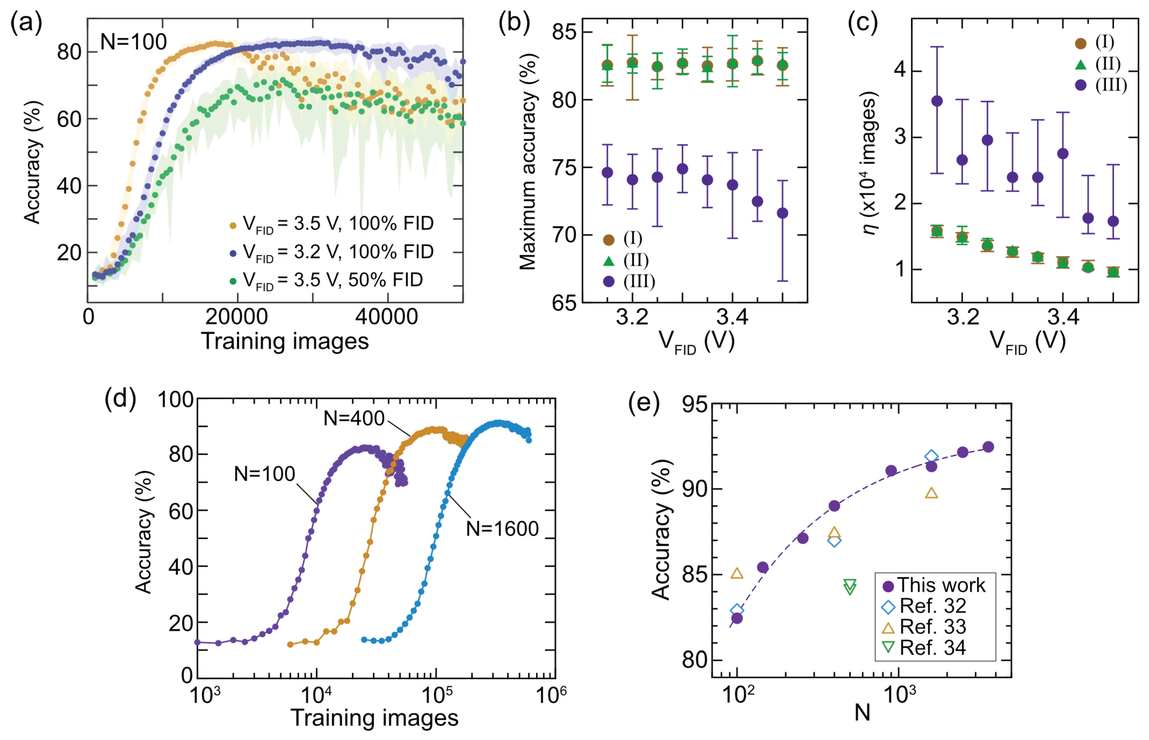
First, let's examine how unsupervised learning, combining STDP and FID, operates using a network with N=100 as an example. In this simulation, when a hidden layer neuron fires, the synapses connected to it are updated by STDP, and subsequently, FID is applied to all synapses that underwent STDP (100% FID). For STDP, we utilized the approximate curve obtained from measurements at VSTDP=3.5 V, and for FID, the approximate curve with VFID varied in the range of 3.15 to 3.5 V was employed. Random variations from the distributions estimated by the measurements were incorporated into both STDP and FID. The training dynamics in Figure 8a show the average classification accuracy over 10 training/classification cycles, with the shaded area indicating the spread between the maximum and minimum values. In comparison to the result at VFID=3.2 V, a higher VFID of 3.5 V reaches maximum accuracy faster, but subsequently experiences more significant accuracy degradation and fluctuates. Here, the number of training images required to reach 90% of the maximum average accuracy is defined as learning efficiency (η). While VFID does not significantly affect the maximum accuracy (Figure 8b), a noticeably larger VFID is advantageous for learning efficiency (Figure 8c). This is presumed to be due to a larger VFID enhancing the WTA effect, suppressing the probability of overlapping different digit patterns. However, as VFID increases, the robustness deteriorates after reaching the maximum accuracy, as shown in Figure 8a, suggesting that a large VFID degrades the information of the pattern once learned. Based on the characteristics of the IDMFET obtained in this experiment, VFID around 3.2 V is considered a balanced and favorable condition.
From the perspective of reducing calculation costs, it is advantageous to minimize the number of FIDs. Figure 8a illustrates the training dynamics of randomly inducing FID pulses with a 50% probability, demonstrating that both the maximum accuracy and learning efficiency are degraded compared to those of the 100% FID. As depicted in Figure 8b,c, no clear benefit was found from the results of VFID dependence either. We also investigated various FID probabilities and concluded that FID is always required after STDP. This result suggests that FID is effective for properly operating WTA and accumulating training patterns' information in appropriate synapses. It is worth mentioning that previously reported studies on STDP-based unsupervised learning did not incorporate additional pulses such as FID [32,33,34,37,38,39,40,41]. This difference is presumed to be due to the difference in spike waveforms. Generally, more complex spike waveforms are employed to balance potentiation and depression during STDP, for example, spike waveforms include triangle waves and different positive/negative shapes, voltages, and widths. In this study, emphasis was placed on the simplicity of spike waveforms and concurrent STDP learning. An important result of this study is that we were able to achieve efficient unsupervised learning by combining additional FIDs within these constraints.
Next, we briefly mention the impact of the variation of IDMFETs. The training and classification calculation without the variation was also performed, but there are no significant differences in classification accuracy and learning efficiency (Figure 8b,c). We performed similar calculations with a wider distribution than the experimentally observed variation of IDMFETs and found a decline in learning performance. For example, if the variation is 10 times wider than those of IDMFETs, the maximum accuracy drops to 70 %. This means that while the current level of variation is acceptable, devices with excessive variation should be treated with caution.
Finally, let's discuss the impact of the feature neuron size. Figure 8e illustrates training dynamics for different values of N, calculated at VFID=3.25 V. Increasing N results in a decrease in learning efficiency due to the increased number of synapses to be learned, where we found a proportional relationship of η=68×N. On the other hand, increasing N can improve classification accuracy, as shown in Figure 8e, in which the previously reported accuracy data deduced by similar networks with STDP-based unsupervised learning were compared [32,33,34]. It is important to note that previous studies were not related to the device characteristics or are not based on the actual device dynamics. It is evident that even with the STDP characteristics of IDMFET, introducing suitable FID operations can achieve accuracy equivalent to conventional SNN. Based on these results, IDMFET is considered a promising candidate as a synaptic device for unsupervised SNN learning. Particularly noteworthy is the fact that, in typical SNN systems, the number of synapses is orders of magnitude larger than that of neurons; therefore, the implementation of high-density synaptic devices using IDMFETs is expected to be highly effective.
4. Conclusions
The HfO2/SiO2-based IDMFETs exhibit nonlinear and asymmetric dynamics of pulse-induced Id modulation, associated with the superimposition of inherent nonlinear and near-symmetric IDM response and FET operation characteristics. STDP-like spike-timing-dependent double-pulse-controlled Id modulation of IDMFETs can be demonstrated, showing nonlinear and asymmetric weight update dynamics. We propose a timing-independent double-pulse-controlled Id depression of IDMFETs as an additional FID weight update for SNN to optimize unsupervised STDP learning. The training and classification of handwritten digits with a two-layer SNN, leveraging the experimentally observed STDP and FID characteristics, reveals the effectiveness of IDMFET synaptic devices for unsupervised learning in SNN.
Author Contributions
Conceptualization, N.M.; methodology, N.M.; formal analysis, N.M.; investigation, N.M.; data curation, N.M.; writing—original draft preparation, N.M.; writing—review and editing, N.M.; supervision, N.M.; project administration, N.M.; funding acquisition, N.M; The author has read and agreed to the published version of the manuscript.
Funding
This work was supported by JSPS KAKENHI Grant Number 16H02335 and 19H02178.
Data Availability Statement
Not applicable.
Acknowledgments
Part of the device fabrication was conducted at the AIST Nano-Processing Facility (AIST-NPF). The author would like to thank the members of the ULVAC-AIST joint research project for valuable discussions and Prof. H. Nohira of Tokyo City University for hard x-ray photoelectron spectroscopy measurements.
Conflicts of Interest
The authors declare no conflict of interest.
References
- Kahng, D.; Atalla, M.M. Silicon-silicon dioxide field induced surface devices. In IRE-AIEE Solid State Device Research Conference; Carnegie Institute of Technology: Pittsburgh, PA, USA, June 1960. [Google Scholar]
- Moore, G.E. Cramming More Components onto Integrated Circuits. Electronics. 1965, 38, 114–117. [Google Scholar] [CrossRef]
- Robertson, J.; Wallace, R.M. High-k materials and metal gates for CMOS applications. Mater. Sci. Eng. 2015, 88, 1–41. [Google Scholar] [CrossRef]
- Choi, J.; Mao, Y.; Chang, J. Development of hafnium based high-k materials-A review. Mater. Sci. Eng. R Rep. 2011, 72, 97–136. [Google Scholar] [CrossRef]
- Radamson, H.H.; Zhu, H.; Wu, Z.; He, X.; Lin, H.; Liu, J.; Xiang, J.; Kong, Z.; Xiong, W.; Li, J.; et al. State of the Art and Future Perspectives in Advanced CMOS Technology. Nanomaterials. 2020, 10, 1555. [Google Scholar] [CrossRef] [PubMed]
- Zhao, C.; Zhao, C.-Z.; Taylor, S.; Chalker, P.-R. Review on non-volatile memory with high-k dielectrics: Flash for generation beyond 32 nm. Materials. 2014, 7, 5117–5145. [Google Scholar] [CrossRef]
- Lu, C.-Y.; Hsieh, K.-Y.; Liu, R. Future challenges of flash memory technologies. Microelectron. Eng. 2009, 86, 283–286. [Google Scholar] [CrossRef]
- Miller, S.L.; McWhorter, P.J. Physics of the ferroelectric nonvolatile memory field effect transistor. J. Appl. Phys. 1992, 72, 5999–6010. [Google Scholar] [CrossRef]
- Tokumitsu, E.; Nakamura, R.; Ishiwara, H. Nonvolatile memory operations of metal-ferroelectric-insulator-semiconductor (MFIS) FETs using PLZT/STO/Si(100) structures. IEEE Electron Device Letters. 1997, 18, 160–162. [Google Scholar] [CrossRef]
- Böscke, T.S.; Müller, J.; Bräuhaus, D.; Schröder, U.; Böttger, U. Ferroelectricity in hafnium oxide thin films. Appl. Phys. Lett. 2011, 99, 102903. [Google Scholar] [CrossRef]
- Park, M.H.; Lee, Y.H.; Mikolajick, T.; Schroeder, U.; Hwang, C.S. ; Review and perspective on ferroelectric HfO2-based thin films for memory applications. MRS Commun. 2018, 8, 795–808. [Google Scholar] [CrossRef]
- Schroeder, U.; Park, M.H.; Mikolajick, T.; Hwang, C.S. The fundamentals and applications of ferroelectric HfO2. Nat. Rev. Mater. 2022, 7, 653–669. [Google Scholar] [CrossRef]
- Trentzsch, M.; Flachowsky, S.; Paul, J.; Reimer, B.; Utess, D.; Jansen, S.; Mulaosmanovic, H.; Müller, S.; Slesazeck, S.; Ocker, J.; et al. A 28nm HKMG super low power embedded NVM technology based on ferroelectric FETs. In Proceedings of the 2016 IEEE International Electron Devices Meeting (IEDM), San Francisco, CA, USA, 3–7 December 2016; pp. 11.5.1–11.5.4. [Google Scholar]
- Mulaosmanovic, H.; Breyer, E.T.; Dünkel, S.; Beyer, S.; Mikolajick, T.; Slesazeck, S. Ferroelectric field-effect transistors based on HfO2: A review. Nanotechnology. 2021, 32, 502002. [Google Scholar] [CrossRef]
- Dutta, S.; Schafer, C.; Gomez, J.; Ni, K.; Joshi, S.; Datta, S. Supervised Learning in All FeFET-Based Spiking Neural Network: Opportunities and Challenges. Front. Neurosci. 2020, 14, 634. [Google Scholar] [CrossRef]
- Yu, S.; Hur, J.; Luo, Y.-C.; Shim, W.; Choe, G.; Wang, P. Ferroelectric HfO2-based synaptic devices: Recent trends and prospects. Semicond. Sci. Technol. 2021, 36, 104001. [Google Scholar] [CrossRef]
- Lin, L.; Robertson, J. Atomic mechanism of electric dipole formed at high-K: SiO2 interface. J. Appl. Phys. 2011, 109, 094502. [Google Scholar] [CrossRef]
- Iwai, H.; Toriumi, A.; Misra, D. High Dielectric Constant Materials for Nanoscale Devices and Beyond. Electrochem. Soc. Interface. 2017, 26, 77–81. [Google Scholar] [CrossRef]
- Kita, K.; Toriumi, A. Origin of electric dipoles formed at high- interface. Appl. Phys. Lett. 2009, 94, 132902. [Google Scholar] [CrossRef]
- Abe, Y.; Miyata, N.; Shiraki, Y.; Yasuda, T. Dipole formation at direct-contact HfO2∕ Si interface. Appl. Phys. Lett. 2007, 90, 172906. [Google Scholar] [CrossRef]
- Miyata, N. Electric-field-controlled interface dipole modulation for Si-based memory devices. Sci. Rep. 2018, 8, 8486. [Google Scholar] [CrossRef] [PubMed]
- Miyata, N.; Sumita, K.; Yasui, A.; Sano, R.; Wada, R.; Nohira, H. Electrically induced change in HfO2/1-monolayer TiO2/SiO2 metal-oxide-semiconductor stacks: Capacitance–voltage and hard X-ray photoelectron spectroscopy studies. Appl. Phys. Express. 2021, 14, 071005. [Google Scholar] [CrossRef]
- Kirihara, Y.; Tsujiguchi, R.; Ito, S.; Yasui, A.; Miyata, N.; Nohira, H. Using hard X-ray photoelectron spectroscopy to study a SiO2/HfO2-based interface dipole modulation stack embedded in a metal–insulator-metal structure. Appl. Phys. Express. 2022, 15, 111003. [Google Scholar] [CrossRef]
- Miyata, N. Low temperature preparation of HfO2/SiO2 stack structure for interface dipole modulation. Appl. Phys. Lett. 2018, 113, 251601. [Google Scholar] [CrossRef]
- Roy, K.; Jaiswal, A.; Panda, P. Towards spike-based machine intelligence with neuromorphic computing. Nature. 2019, 575, 607–617. [Google Scholar] [CrossRef] [PubMed]
- Ielmini, D.; Wang, Z.; Liu, Y. Brain-inspired computing via memory device physics. APL Mater. 2021, 9, 050702. [Google Scholar] [CrossRef]
- Hasler, J.; Marr, H. Finding a roadmap to achieve large neuromorphic hardware systems. Front. Comput. Neurosci. 2013, 7, 118. [Google Scholar] [CrossRef] [PubMed]
- Pan, W.-Q.; Chen, J.; Kuang, R.; Li, Y.; He, Y.-H.; Feng, G.-R.; et al. Strategies to Improve the Accuracy of Memristor-Based Convolutional Neural Networks. IEEE Trans. Electron. Devices. 2020, 67, 895–901. [Google Scholar] [CrossRef]
- Aabrar, K.A.; Gomez, J.; Kirtania, S.G.; Jose, M.S.; Luo, Y.; Ravikumar, P.G.; Ravindran, P.V.; Ye, H.; Banerjee, S.; Dutta, S. BEOL compatible superlattice FerroFET-based high precision analog weight cell with superior linearity and symmetry. In Proceedings of the 2021 IEEE International Electron Devices Meeting (IEDM), San Francisco, CA, USA, 3–7 December 2021; 19.6.1–19.6.4; pp. 19.6.1–19.6.4. [Google Scholar]
- Nandakumar, S.R.; Boybat, I.; Le Gallo, M.; Eleftheriou, E.; Sebastian, A.; Rajendran, B. Experimental Demonstration of Supervised Learning in Spiking neural networks with phase-change Memory Synapses. Sci. Rep. 2020, 10, 8080. [Google Scholar] [CrossRef]
- Yang, S.-T.; Li, X.-Y.; Yu, T.-L.; Wang, J.; Fang, H.; Nie, F.; He, B.; Zhao, L.; Lü, W.-M.; Yan, S.-S.; et al. High-Performance Neuromorphic Computing Based on Ferroelectric Synapses with Excellent Conductance Linearity and Symmetry. Adv. Funct. Mater. 2022, 32, 2202366. [Google Scholar] [CrossRef]
- Diehl, P. U.; Cook, M. Unsupervised learning of digit recognition using spike-timing-dependent plasticity. Front. Comput. Neurosci. 2015, 9, 99. [Google Scholar] [CrossRef]
- Shrestha, A.; Ahmed, K.; Wang, Y.; Qiu, Q. Stable spike-timing dependent plasticity rule for multilayer unsupervised and supervised learning. In Proceedings of the International Joint Conference on Neural Networks (IJCNN), Anchorage, AK, USA, 14–19 May 2017; pp. 1999–2006. [Google Scholar]
- Brivio, S.; Ly, D.R.B.; Vianello, E.; Spiga, S. Non-linear Memristive Synaptic Dynamics for Efficient Unsupervised Learning in Spiking Neural Networks. Front. Neurosci. 2021, 15, 580909. [Google Scholar] [CrossRef]
- Izhikevich, E. Simple model of Spiking Neurons. IEEE Trans. Neural Netw. 2003, 14, 1569–1572. [Google Scholar] [CrossRef]
- Yamazaki, K.; Vo-Ho, V.K.; Bulsara, D.; Le, N. Spiking neural networks and their applications: A Review. Brain Sci. 2022, 12, 863. [Google Scholar] [CrossRef] [PubMed]
- Wang, W.; Pedretti, G.; Milo, V.; Carboni, R.; Calderoni, A.; Ramaswamy, N.; Spinelli, A.S.; Ielmini, D. Learning of spatiotemporal patterns in a spiking neural network with resistive switching synapses. Sci. Adv. 2018, 4, eaat4752. [Google Scholar] [CrossRef] [PubMed]
- Saïghi, S.; Mayr, C.G.; Serranogotarredona, T.; Schmidt, H.; Lecerf, G.; Tomas, J.; Grollier, J.; Boyn, S.; Vincent, A.F.; Querlioz, D.; et al. Plasticity in memristive devices for spiking neural networks. Front. Neurosci. 2015, 9, 51. [Google Scholar] [CrossRef]
- Kim, C.-H.; Lee, S.; Woo, S.Y.; Kang, W.-M.; Lim, S.; Bae, J.-H.; Kim, J.; Lee, J.-H. Demonstration of unsupervised learning with spike-timing-dependent plasticity using a TFT-type NOR Flash memory array. IEEE Trans. Electron Devices. 2018, 65, 1774–1780. [Google Scholar] [CrossRef]
- Kaneko, Y.; Nishitani, Y.; Ueda, M. Ferroelectric artificial synapses for recognition of a multishaded image. IEEE Trans. Electron Devices. 2014, 61, 2827–2828. [Google Scholar] [CrossRef]
- Han, H.; Yu, H.; Wei, H.; Gong, J.; Xu, W. Recent Progress in Three-Terminal Artificial Synapses: From Device to System. Small. 2019, 15, 1900695. [Google Scholar] [CrossRef]
- Miyata, N. Study of Direct-Contact HfO2/Si Interfaces. Materials. 2012, 5, 512–527. [Google Scholar] [CrossRef]
- Miyata, N.; Ishii1, H.; Itatani, T.; Yasuda, T. Electron Mobility Degradation and Interface Dipole Formation in Direct-Contact HfO2/Si Metal–Oxide–Semiconductor Field-Effect Transistors. Appl. Phys. Express. 2011, 4, 101101. [Google Scholar] [CrossRef]
- Asanuma, S.; Sumita, K.; Miyaguchi, Y.; Horita, K.; Masuda, T.; Jimbo, T.; Miyata, N. Exploring thermally stable metal-oxide/SiO2 stack for metal oxide semiconductor memory and demonstration of pulse controlled linear response. Appl. Phys. Express. 2023, 16, 061005. [Google Scholar] [CrossRef]
- Lécun, Y.; Bottou, L.; Bengio, Y.; Haffner, P. Gradient-based learning applied to document recognition. Proceedings of the IEEE. 1998, 86, 2278–2324. [Google Scholar] [CrossRef]
- Iakymchuk, T.; Rosado-Muñoz, A.; Guerrero-Martínez, J.F.; Bataller-Mompeán, M.; Francés-Víllora, J.V. Simplified spiking neural network architecture and STDP learning algorithm applied to image classification. EURASIP J. Image Video Process. 2015, 4, 1–11. [Google Scholar] [CrossRef]
- Agarwal, S.; Plimpton, S.J.; Hughart, D.R.; Hsia, A.H.; Richter, I.; Cox, J.A.; James, C.D.; Marinella, M.J. Resistive memory device requirements for a neural algorithm accelerator. In Proceedings of the 2016 International Joint Conference on Neural Networks (IJCNN), Vancouver, BC, Canada, 24–29 July 2016; pp. 929–938. [Google Scholar]
- Kim, M.K.; Lee, J.S. Ferroelectric Analog Synaptic Transistors. Nano Lett. 2019, 19, 2044–2050. [Google Scholar] [CrossRef]
- Hauser, J.R; Ahmed, K. Characterization of ultra-thin oxides using electrical C-V and I-V measurements. AIP Conf. Proc. 1998, 449, 235–239. [Google Scholar]
- McPherson, J.; Kim, J.-Y.; Shanware, A.; Mogul, H. Thermochemical description of dielectric breakdown in high dielectric constant materials. Appl. Phys. Lett. 2003, 82, 2121–2123. [Google Scholar] [CrossRef]
- McPhersona, J.W. Extended Mie-Grüneisen molecular model for time dependent dielectric breakdown in silica detailing the critical roles of O−Si≡O3 tetragonal bonding, stretched bonds, hole capture, and hydrogen release. J. Appl. Phys. 2006, 99, 083501. [Google Scholar] [CrossRef]
- Sze, S.M. Physics of Semiconductor Devices, 2nd ed.; Wiley-Interscience Publication: USA, 1981; pp. 438–448. [Google Scholar]
Figure 1.
Basis of the interface dipole modulation (IDM) mechanism and MOS capacitor characteristics. (a) Proposed IDM mechanism for the HfO2/SiO2 interface with an atomically thin TiO2 modulation layer. (b) High-frequency C-V curve of the HfO2/SiO2/n-Si IDMMOS capacitor displaying counterclockwise hysteresis. (c) Relationship between Vfb shift from the initial Vfb and the maximum and minimum Vg in C-V measurements.
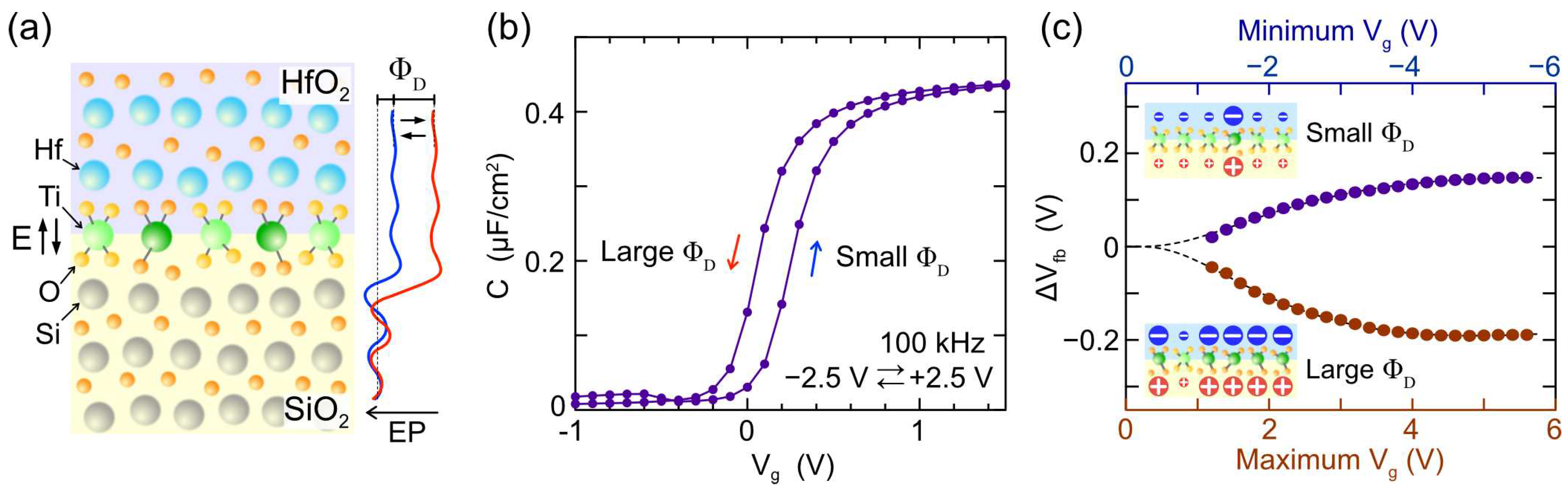
Figure 2.
Illustration of spiking neuron model and network architecture for pattern recognition examined in this study. (a) Spike-based neuron model with leaky integrate-and-fire (LIF) dynamics and spike-timing-dependent plasticity (STDP) synaptic learning. (b) Network architecture where feature synapses are trained through an unsupervised learning based on the experimentally observed pulse responses of IDMFET.
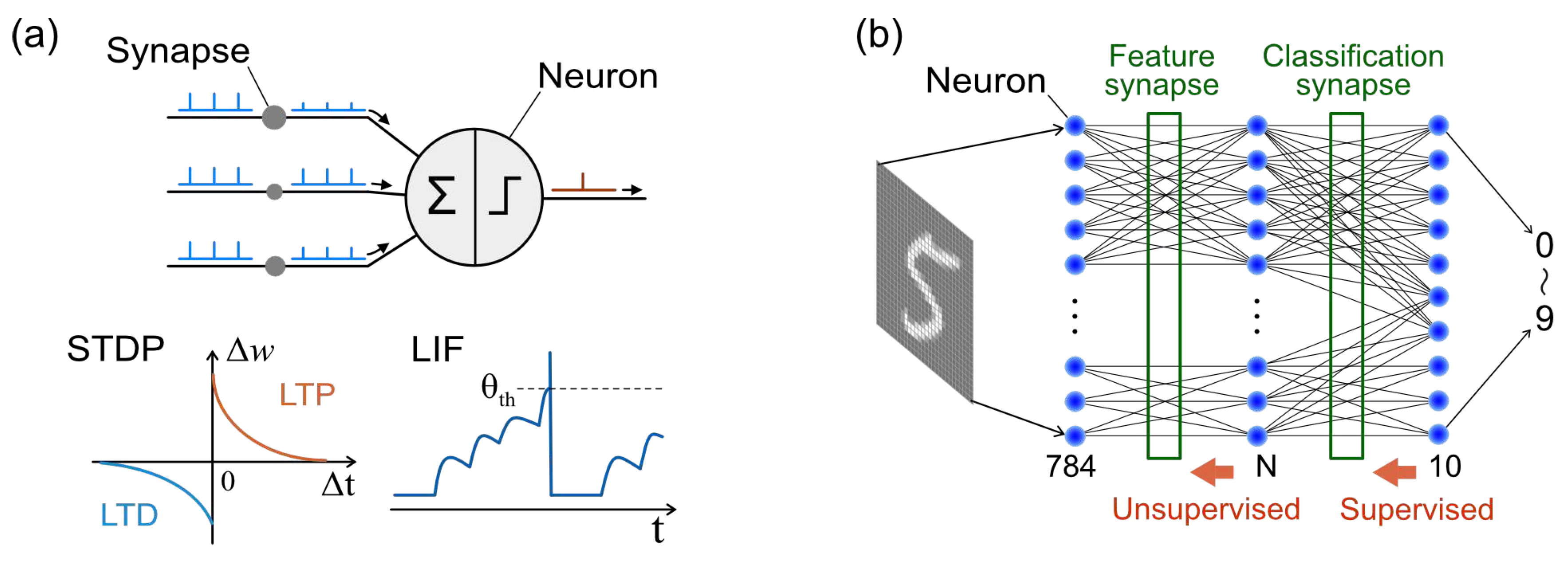
Figure 3.
Pulse response of IDMMOS capacitor with two TiO2 modulation layers. (a) Cyclic characteristics of flat-band voltage (Vfb) shifts, showing stable modulation amplitude and nonlinear characteristics. (b) Dependence of Vfb modulation characteristics on pulse voltage (Vp). (c) Impact of Vp on modulated Vfb shifts and nonlinear parameters (ν+ and ν−).
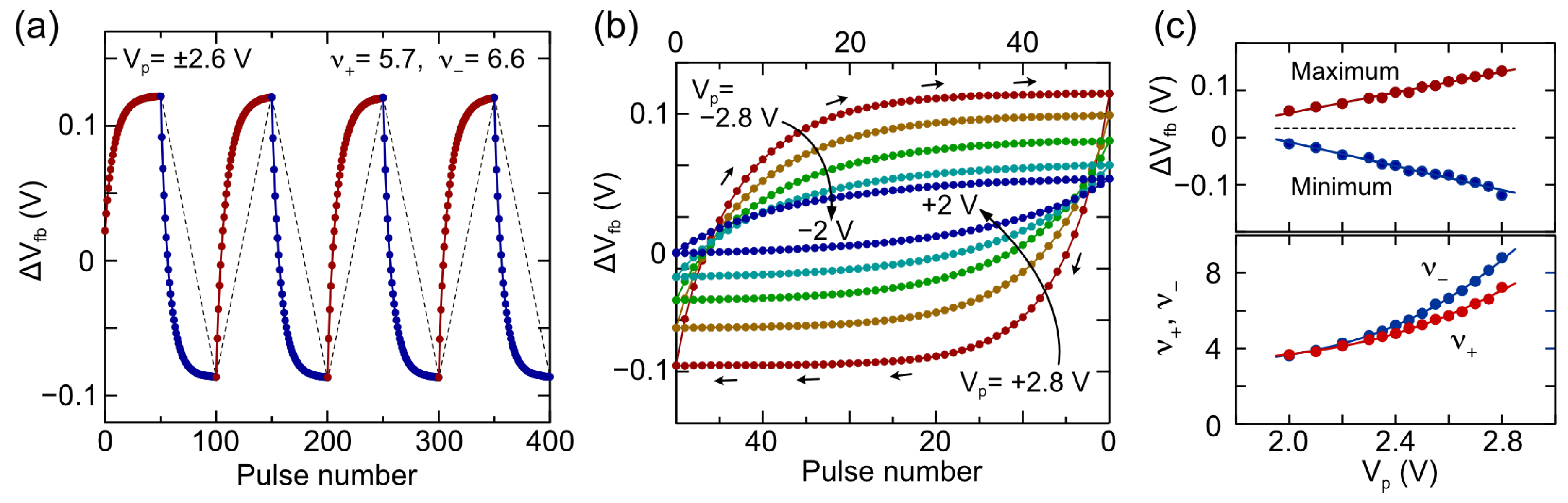
Figure 4.
Pulse response characteristics and IDMMOS capacitor and origin of nonlinear response. (a) Dependence of the rate of Vfb shifts (dVfb/dt) on the ratio of switchable unit dipoles (θD) observed for positive Vfb shifts. (I) and (II) depict the estimated ideal dVfb/dt for θD=0.65 and 0.35, respectively. (b) and (c) θD dependence of zero-field effective activation energy ( and effective dipole moment (peff) for positive and negative Vfb shifts, respectively.
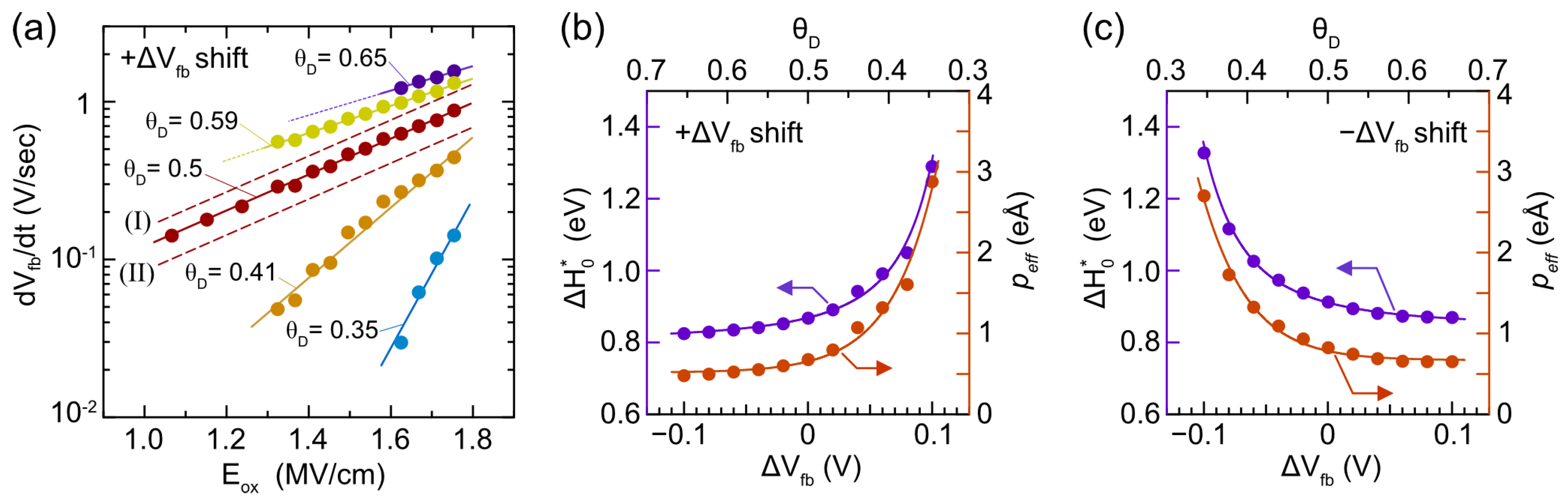
Figure 5.
Pulse-induced drain current (Id) change of IDMFET. (a) DC Id–Vg hysteresis curve and Id modulation amplitude measured under various read gate voltage conditions (I)-(III). (b) Pulse-induced Id changes with a pulse voltage (Vp) of ±5.4 V. Estimated nonlinear parameters for Id increase (ν+) and Id decrease (ν−) are shown. (c) Impact of Vp on nonlinear asymmetric Id responses observed under read conditions (II) in (a). (d) Vp dependence of ν+, ν−, and the ratio of ν+/ν− under various read conditions. (e) Correlation between asymmetric characteristics, ν+/ν−, and the ratio of maximum to minimum drain current (Imax/Imin).
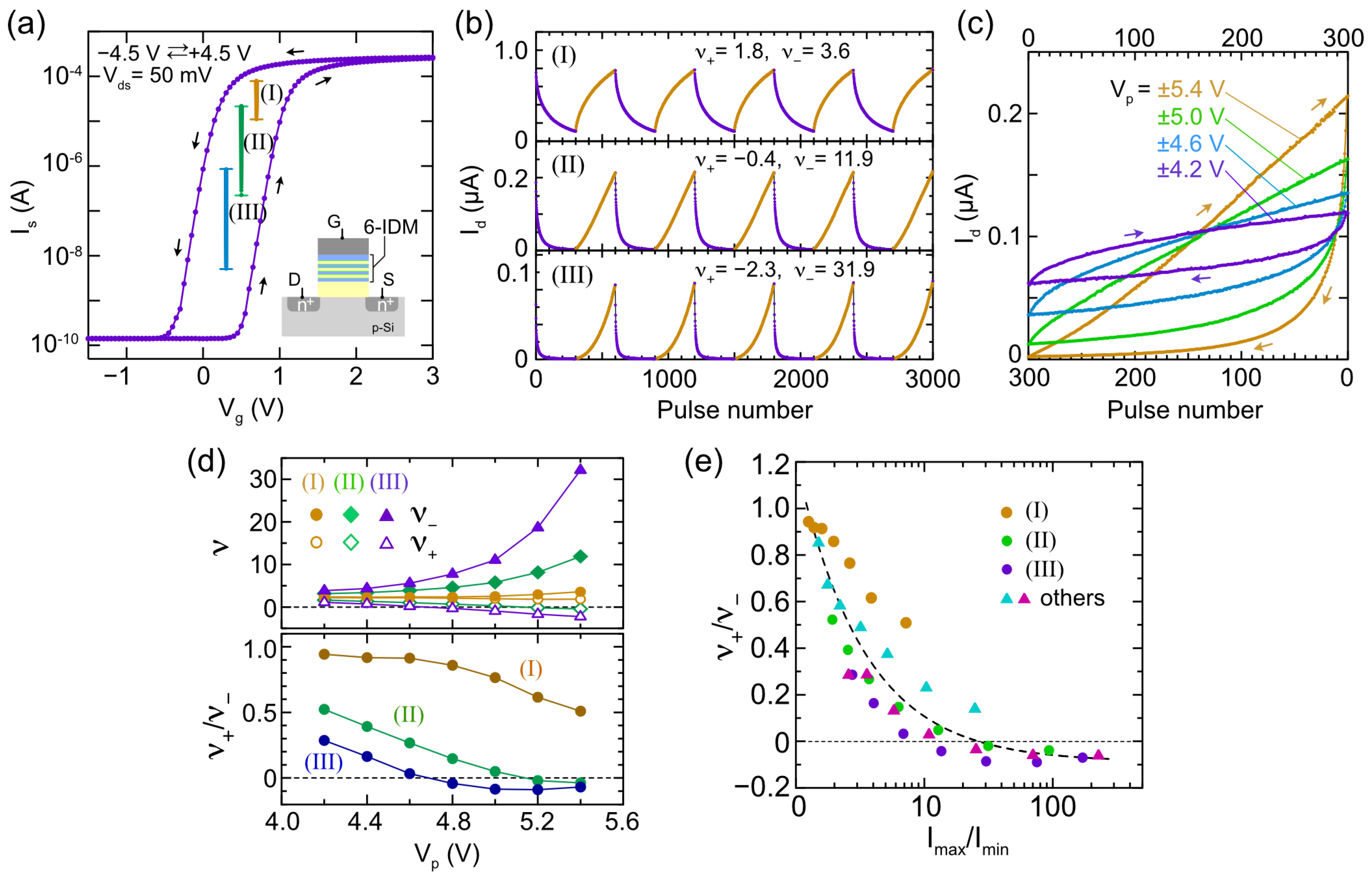
Figure 6.
Double-pulse-controlled STDP operation with a bipolar rectangular waveform. (a) Concurrent STDP drain current (Id) modulation scheme of IDMFET based on the interaction of pre- and post-synaptic waveforms. (b) Demonstration of STDP-like Id modulation. Id changes depend on the spike timing difference (Δt), and nonlinear characteristics persist even during STDP operation. ΔVSTDP waveforms, estimated from the difference between the pre- and post-synaptic waveforms for set Δt conditions, are shown as insets.
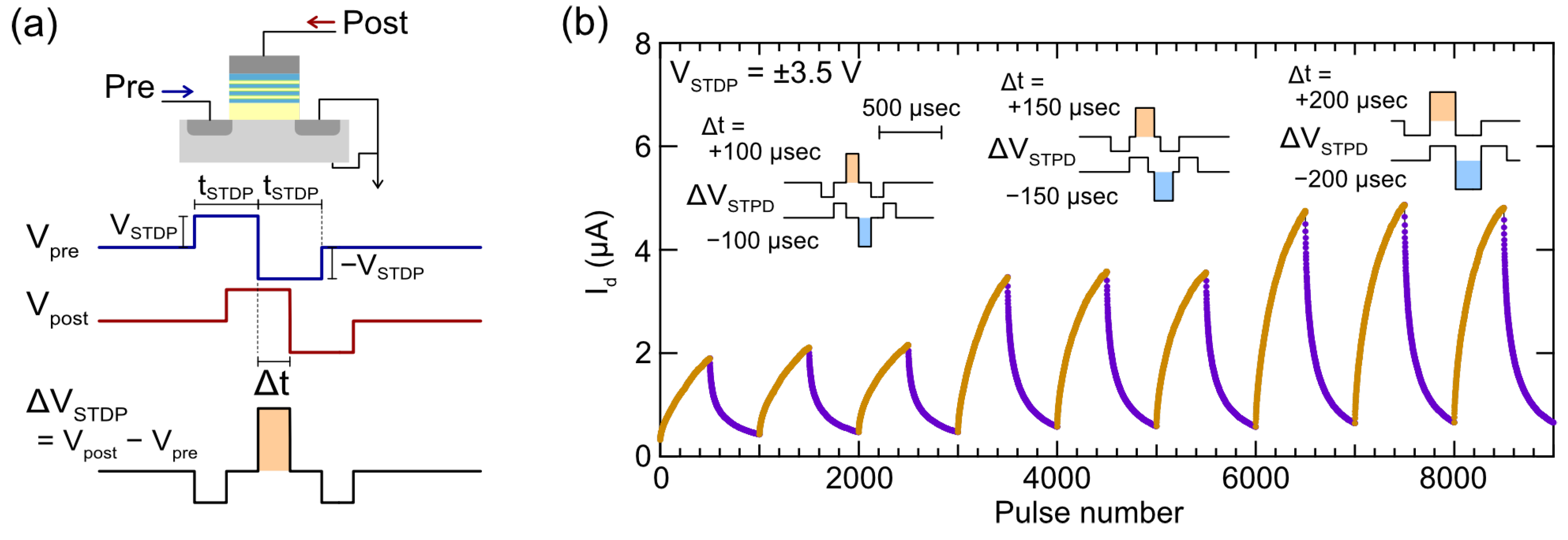
Figure 7.
Double-pulse-induced Id modulation observed within a current range limited to 3.0-0.8 μA. (a) Characteristics of STDP Id modulation observed for Δt=±200 μsec and Δt=±100 μsec. (b) ΔId-Id characteristics derived from STDP Id modulation data, with solid lines representing fitting curves. (c) Δw-Δt characteristics converted from measured ΔId-Id showing nonlinear and asymmetric STDP responses of IDMFET. (d) Variation of Δw for STDP response of IDMFET with Δt=±200 μsec from fitting curves (Δw0). (e) Δw-w characteristics derived from double-pulse-induced Id response with unipolar rectangular waveforms, which were utilized as a frequency independent depression (FID) synaptic update.
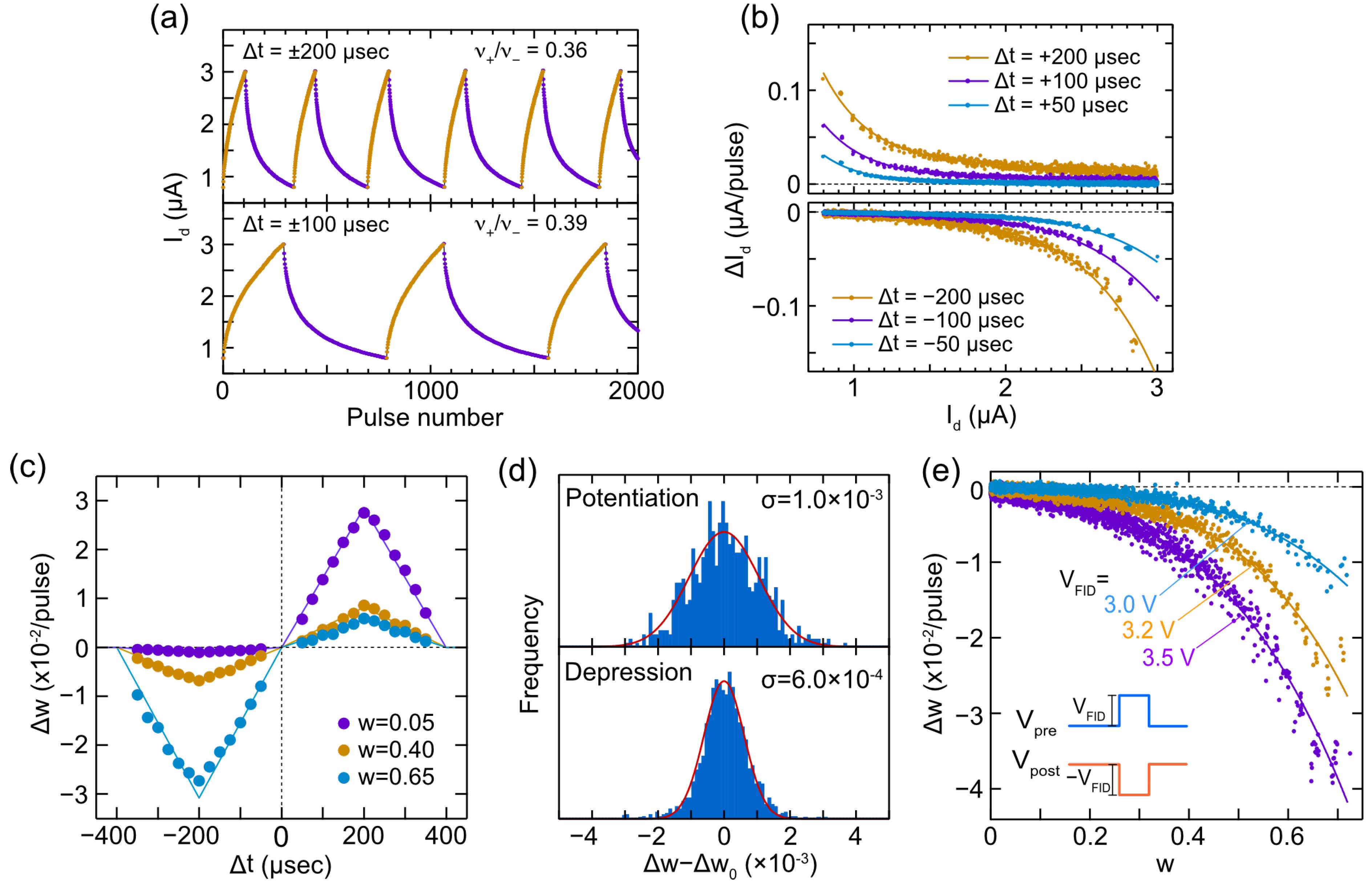
Figure 8.
Demonstration of SNN pattern recognition using IDMFET-based STDP and FID synaptic updates. (a) Simulated training dynamics for N=100 hidden neurons. Comparison of 100% FID spike probability conditions with VFID=3.5 V and 3.2 V. Additionally, the 50% FID spike probability condition with VFID=3.5 V is presented. (b) Impact of VFID on maximum accuracy. (I) and (II) show the results for the 100% FID spike probability condition with and without variations in the IDMFET response, respectively, and (III) show the results for the 50% FID spike probability condition. (c) VFID dependence of learning efficiency (η), where η is defined as the number of training images reaching 90% of the maximum accuracy. (d) Training dynamics performed for different N networks. (e) Dependence of accuracy on N, including relevant references (refs. [32,33,34]) for comparison.
Disclaimer/Publisher’s Note: The statements, opinions and data contained in all publications are solely those of the individual author(s) and contributor(s) and not of MDPI and/or the editor(s). MDPI and/or the editor(s) disclaim responsibility for any injury to people or property resulting from any ideas, methods, instructions or products referred to in the content. |
© 2024 by the authors. Licensee MDPI, Basel, Switzerland. This article is an open access article distributed under the terms and conditions of the Creative Commons Attribution (CC BY) license (http://creativecommons.org/licenses/by/4.0/).
Copyright: This open access article is published under a Creative Commons CC BY 4.0 license, which permit the free download, distribution, and reuse, provided that the author and preprint are cited in any reuse.


