

Submitted:
23 December 2023
Posted:
25 December 2023
You are already at the latest version
Abstract
In this work, nanocomposite photoelectrodes of the TiO2/ Au composition were manufactured, in which the size of plasmonic Au nanoparticles was varied, and the morphology of the TiO2 layer, depending on the thickness, changed from an island to a continuous layer. The influence of the morphology of plasmonic Au nanoparticles and the TiO2 layer on the optical and photoelectrochemical characteristics of hybrid photoelectrodes was studied. It has been shown that continuous coating of Au nanoparticles with a TiO2 layer (layer thickness 10 and 15 nm) leads to a decrease in the photoelectric response, and the decrease in photocurrent density and photoconversion efficiency decreases in proportion to the thickness of the TiO2 layer. The indicated drop in characteristics when plasmonic particles are located under the TiO2 layer is presumably associated with the scattering and recombination of charge carriers in the semiconductor layer. The best performance was shown by a system in which large Au nanoparticles (10 nm) are coated with a 5 nm thick layer of titanium dioxide; in this geometry, Au nanoparticles are decorated with TiO2 nanoparticles, as a result of which the photoelectrode-electrolyte interface has a more complex structure.
Keywords:
Photoelectrochemistry
; surface plasmon resonance
; atomic layer deposition
; magnetron sputtering
; titanium oxide
; Au nanoparticles
; thin film
; photoelectrode
Introduction
Increasing the efficiency of photoelectrochemical processes, such as photocatalytic decomposition of water [1], photosynthesis [2], photocatalytic purification of water from pollutants [3] using plasmonic nanoparticles deposited on wide-gap semiconductor photoelectrodes, is a well-known technique for a wide range of materials, for example: [4,5], ZnO [6,7], WO3 [8], SnO2 [9], as well as more complex oxide compounds: BiVO4 [10,11], CuWO4 [12], ZnFe2O4 [13] and many others, Semiconductor materials for photoelectrochemical applications are presented and classified in more detail in detailed reviews [14,15].
The following materials were considered for plasmonic nanoparticles: Au [16,17]; Ag [18]; Pt [19], Al [20], TiN [21]. Varying the material of plasmonic particles, their size and shape, is a key tool for tuning the spectral properties of a photoelectrode [22,23,24]. Methods for applying plasmonic nanoparticles to a semiconductor are divided into chemical and physical. Chemical methods include: direct chemical reduction of the corresponding metals on the surface of the semiconductor [25,26], hydrothermal/solvothermal synthesis [27], photodeposition [28,29]. Physical methods include magnetron [30] or thermal [31] sputtering of metal targets.
From the point of view of the mechanism of influence of plasmonic nanoparticles, modern ideas assign three possible mechanisms for the influence of plasmonic nanoparticles on photoelectrochemical processes [32]. The first mechanism is the injection of hot charge carriers from a metal particle into a semiconductor direct [33] and indirect [34] mechanism. The second mechanism is plasmon-induced resonant energy transfer [35], which consists in the non-radiative transfer of excitation energy from a plasmonic particle directly to a semiconductor with the subsequent generation of an electron-hole pair participating in a chemical transformation; The third mechanism of influence is scattering, usually through a dielectric layer, this is observed in core-shell systems [36].
One of the weaknesses of this concept is the fact that plasmonic nanoparticles obtained by both physical and chemical methods are weakly bound to the surface of the semiconductor, as a result of which the photoelectrode can be easily damaged. Mechanical stability can be improved by introducing particles into the semiconductor layer. In this work, we plan to consider the relationship between the morphology of Au nanoparticles and the TiO2 layer (either island or layer-by-layer) and the photoelectrochemical properties of nanocomposite photoelectrodes. In Figure 1 shows the technological process of manufacturing nanocomposite photoelectrodes with Au nanoparticles and different morphology of the TiO2 layer (either island or layer-by-layer).
2. Materials and methods
2.1. Materials
An ITO film on a glass substrate was used as a transparent electrode; the surface resistance of the coating was equal to 8 Ω/sq. To form film structures using the ALD method, Titanium ethoxide (Ti4(OCH2CH3)16) and DI water were used. To form a layer of gold nanoparticles using magnetron sputtering, a gold target (99.99%) was used. Sodium chloride (NaCl), sodium sulfide (Na2S) were used for photoelectrochemical measurements. All chemical reagents were chemical grade.
2.2. Magnetron sputtering Au film on ITO/glass substrate
A layer of gold with a thickness of 5 nm and 10 nm is deposited onto a glass substrate with an ITO (indium tin oxide) layer using vacuum deposition. Sputtering mode: direct current with power stabilization (50 W). In this case, the substrate repeatedly passes by the magnetron with an interval of 6 seconds. This approach ensures uniformity and controlled film thickness, where 2.5 nm of gold is deposited per pass, which significantly affects the final characteristics of the resulting coverings.
2.3. Thermal annealing Au film, formation Au nanoparticles
Then the substrate with a thin layer of gold is annealed in an oven for 1 hour. The first part of the samples was annealed at a temperature of 450 °C. ITO is poorly wetted by molten gold, so that as a result of annealing, the gold layer melts and disperses into many separate droplets. Subsequent cooling of the substrate leads to crystallization of the droplets and the formation of gold particles on the specified substrate.
2.4. Atomic layer deposition TiO2 film on Au/ITO/glass substrate
Titanium dioxide is deposited onto a glass substrate with an ITO layer using the atomic layer deposition (ALD) method using a Picosun 300 (Picosun Oy, Espoo, Finland). Titanium ethoxide served as a titanium precursor, and ionized H2O vapor acted as an oxygen source. Nitrogen N2 of high purity 99.9999% was used as a carrier gas. According to the calibration, the thickness of the TiO2 layers is: 5 nm (150 deposition cycles), 10 nm (300 deposition cycles) and 15 nm (450 deposition cycles). A complete list of samples of the Au/TiO2/ITO photoelectrode series is given in Table 1.
2.5. Scanning Electron Microscopy (SEM) and EDS analysis
The morphology of the TiO2/ITO and TiO2/Au/ITO films was studied using the FE-SEM method on a S-5500 (Hitachi, Tokyo, Japan); the accelerated voltage was 3 kV. EDS analysis was carried out using a TM4000 Plus (Hitachi, Tokyo, Japan) equipped with a Bruker X-Flash 630Hc (Bruker, Billerica, MA, USA) detector, the accelerating voltage during mapping was 20 kV at maximum current (mode 4), the accumulation time was 5 min.
2.6. Optical Properties Measurements
The optical density spectra for the TiO2/ITO/glass and Au/TiO2/ITO/glass photoelectrode samples were measured in the range of 400–700 nm on a UV 3600 spectrophotometer (Shimadzu, Kyoto, Japan). The measurements were carried out using an aperture 10 mm in diameter and a resolution of 1 nm.
2.7. Photoelectrochemical measurements
The photoelectrochemical properties of the samples were studied in a two-electrode cell. The photoelectrodes under study were used as the working electrode. Cu2S deposited on brass served as the counter electrode. The counter electrode was obtained by treating brass for an hour with concentrated hydrochloric acid at 70 °C, rinsing with distilled water and immersing it in a 1 M aqueous solution of sodium sulfide for fifteen minutes [37]. A solution consisting of 1 M Na2S, 1 M S (hereinafter designated as 1 M Na2Sn) and 0.1 M NaCl was used as an electrolyte [38]. The electrodes were compressed to optimize contact. Photovoltaic characteristics were measured using a potentiostat-galvanostat R-45X (Russia) with an electrochemical impedance measuring module FRA-24M in the voltage range from -0.8 to +0.8 V, at a potential sweep rate of 0.02 V/s. Measurements using impedance spectroscopy were carried out in the frequency range 0.8 – 105 Hz with an amplitude of 10 mV at a constant potential value of 0.2 V. Mott-Schottky dependences were studied in the voltage range from -0.6 V to 0.7 V with an amplitude of 10 mV at a constant frequency, equal to 1000 Hz. In all experiments, a 450-LED light-emitting diode with a wavelength of 450 nm and a radiation power of 19.2 mW/cm2 was used as a light source. The area of the illuminated surface in the cell was 1 cm2. It should be noted that the radiation absorption peak of the studied samples lies in the ultraviolet region of the spectrum, while for the studies we used an LED emitting in the violet region. This causes relatively low efficiency values for converting light energy into electrical energy. However, for the purposes of the work (comparative assessment of samples), these measurements seem sufficient.
3. Results and discussion
3.1. EDS analysis and morphology TiO2/ITO/glass photoelectrodes
Figure 2a shows EDS spectra TiO2/ITO/glass photoelectrodes with a TiO2 layer thickness of 15 nm. In the EDS spectrum, one can clearly distinguish lines belonging to the elements of each photoelectrode layer, so the Kα1 line of silicon with an energy of 1.740 keV, the Kα1 line of sodium with an energy of 1.040 keV, the Kα1 line of magnesium with an energy of 1.254 keV and the Kα1 line of aluminum with an energy of 1.486 keV belong to the glass substrate. The ITO transparent conductor layer contains lines with energies of 3.286 keV, 3.487 keV, 3.712 keV and 3.920 keV, which correspond to the Lα1, Lβ1, Lβ2 and Lγ1 series of indium, respectively. The tin lines doped with ITO at a level of ~10% have energies of 3.444 keV, 3.663 keV, 3.904 keV, which can be attributed to Lα1, Lβ1, Lβ, however, as can be seen from the spectrum, the tin lines partially overlap with the indium lines, resulting in they cannot be separated on a spectrum.
The titanium oxide layer corresponds to lines with energies of 4.512 keV and 4.933 keV, which correspond to the Kα1 and Lβ1 series of titanium (Figure 2a). An increase in the number of ALD cycles of TiO2 deposition from 150 to 450 cycles is accompanied by an increase in the intensity of the peaks. This fact is clear evidence of an increase in the thickness of the TiO2 film. The line with an energy of 0.525 keV corresponds to the Kα1 series of oxygen, which is present in all three layers of the photoelectrodes under consideration.
Figure 3 shows SEM images of TiO2 layers, 5, 10 and 15 nm thick, on ITO/glass substrate. All films are characterized by TiO2 and have a polycrystalline structure; crystallites are characterized by spherical and needle-shaped morphology. Spherical crystallites have sizes in the range of 20-60 nm, while needle-shaped ones have a size of 40-60 nm and a length of 50-150 nm.
TiO2 films have a domain structure, which is probably caused by the polycrystallinity of the ITO film on which the TiO2 layer is deposited. This morphology is typical for the ALD method [39].
3.2. Optical properties TiO2/ITO/glass photoelectrodes
Figure 4 shows the transmission spectra for TiO2/ITO/glass photoelectrodes with different TiO2 thicknesses.
The spectral transmittance of all three TiO2/ITO/glass photoelectrodes is associated with reflection, which is characteristic of ITO film. The effect of TiO2 on the spectrum is associated with a total decrease in the transmittance of the photoelectrode, which decreases with increasing thickness of the TiO2 film.
3.3. EDS analysis and morphology TiO2/Au/ITO/glass photoelectrodes
Figure 5 shows the EDS spectra of TiO2/Au/ITO/glass photoelectrodes with a TiO2 layer thickness of 15 nm and different thicknesses of the dispersed gold layer of 5 nm (Figure 5a) and 10 nm (Figure 5b).
The general pattern of spectral lines looks similar to TiO2/ITO/glass photoelectrodes, with the exception that peaks with energies of 2.193 keV and 2.203 keV are observed, which correspond to the Mα1 and Mβ series of gold.
Figure 6 shows SEM images of TiO2/Au (5 nm)/ITO/glass and TiO2/Au (10 nm)/ITO/glass nanocomposite photoelectrodes, with different thicknesses of Au films and a TiO2 layer at different magnifications.
Based on the SEM data, the following conclusions can be drawn: firstly, gold films with a thickness of 5 and 10 nm are dispersed during the annealing process at 450 °C due to the effect of dimensional melting. Poor wetting of the ITO substrate by molten gold leads to the fact that it is energetically favorable for gold to coalesce into droplets. Moreover, the thickness of the initial gold film determines the particle size after annealing. According to the SEM of a 5 nm thick Au film, after annealing the particles have high polydispersity, this is typical for this process. The particles have sizes from 10 to 60 nm. For an Au film with a thickness of 10 nm, the particles have a significantly larger size from 20 to 200 nm, therefore the scatter in particle sizes is even greater than for a Au film with a thickness of 5 nm.
The second important aspect of SEM studies is understanding how the TiO2 film covers gold nanoparticles and what morphology it has in the case of nanocomposite photoelectrodes. A detailed study of the surface of Au nanoparticles shows that in the case of a TiO2 film 5 nm thick, there is no continuous coating of the surface of both particles based on 5 nm and 10 nm Au films. Only decoration of Au particles and TiO2 particles is observed. An increase in the thickness of the TiO2 film leads to a greater degree of coverage of the surface of Au nanoparticles with TiO2 nanoparticles. One can even assume a transition from an island coating to a continuous one. Moreover, the morphologies of TiO2/Au (5 nm)/ITO and TiO2/Au (10 nm)/ITO are similar for TiO2 thicknesses of 10 and 15 nm, respectively.
The morphology of the TiO2 layer in the spaces between Au nanoparticles is also different from continuous TiO2 films. For TiO2/Au (5 nm)/ITO the crystallites have only a spherical shape; the needle-shaped morphology of the crystallites is not observed for all TiO2 thicknesses. For TiO2/Au (10 nm)/ITO, crystallites of both spherical and needle-shaped morphology are visible in the spaces between Au particles, thus the average distance between Au particles has a strong influence on the morphology of TiO2 films.
3.4. Optical properties TiO2/Au/ITO/glass photoelectrodes
Figure 7 shows the spectral transmittance of TiO2/Au (5 nm)/ITO/glass и TiO2/Au (10 nm)/ITO/glass photoelectrodes with different TiO2 layer thicknesses
The transmission spectra for two types of photoelectrodes show resonant absorption associated with the excitation of plasmons in spherical gold nanoparticles. Moreover, the position of the absorption peak is related both to the average size of nanoparticles and to the dielectric constant of their environment.
For TiO2/Au (5 nm)/ITO/glass with a TiO2 thickness of 5 nm, the resonant wavelength is 640 nm. An increase in the thickness of the TiO2 layer leads to a shift of the absorption peak to the red region; the resonance wavelengths are 665 nm and 677 nm, respectively. For TiO2/Au (10 nm)/ITO/with a TiO2 thickness of 5 nm, the resonance wavelength is 706 nm. An increase in the thickness of TiO2 leads to a shift of the absorption peak to the red region; the resonance wavelengths are 750 nm and 775 nm, respectively.
The shift in the plasmon resonance frequency to a longer wavelength region in gold nanoparticles for each line of photoelectrodes is due to the gradual coating of Au nanoparticles with a TiO2 layer, which leads to a change in the local dielectric constant near the particle. Thus, we can conclude that increasing the thickness of TiO2 from 10 nm to 15 nm leads to an increase in the continuity of the coating of Au nanoparticles. This result is in good agreement with the theoretical dependence of the plasmon resonance frequency on the dielectric constant of the medium in which the particle under study is located.
The width of the absorption line is related to the polydispersity of Au nanoparticles; the higher it is, the wider the absorption line. Thus, for TiO2/Au (5 nm)/ITO/glass, the absorption peak width is significantly narrower than for TiO2/Au (10 nm)/ITO/glass, which confirms our conclusions drawn from the analysis of the SEM image.
3.5. Photoelectrochemical properties of TiO2/ITO/glass photoelectrodes
Figure 8 shows voltammograms of the TiO2/ITO/glass photoelectrodes under study. We classify photoelectrodes as the first series of samples depending on the thickness of the TiO2 layer; they have the nomenclature: 1-1 (5 nm TiO2), 1-2 (10 nm TiO2) and 1-3 (15 nm TiO2). The voltammogram contains peaks around -0.6 V for all samples and a lower intensity peak around -0.4 V.
From the voltammetry data, the photovoltaic characteristics of the samples were calculated; they are presented in Table 2. It should be noted that the short-circuit current densities for all samples without gold particles are low and decrease with increasing thickness of the titanium dioxide layer. The open circuit potential varies with different samples, but the nature of these changes is difficult to determine. Most often, this is due to a change in the position of the level of the conduction band of the samples and the peculiarities of the formation of a double electrical layer at the electrode/electrolyte interface. The filling factor value gradually increases with increasing TiO2 thickness. The efficiency values for converting light energy into electrical energy are quite low and do not exceed 0.004% for a TiO2 film 5 nm thick.
Samples in this series are comparison samples. The short circuit current density and efficiency for all samples in the series are low. Sample 1-1 (TiO2 (5 nm)/ITO/glass) has the best results-light energy conversion is carried out with an efficiency of ~0.004%, while the photocurrent density is 0.005 mA/cm2. The worst sample of series 1-3 (TiO2 (15 nm)/ITO/glass) has an efficiency of 0.002% at a photocurrent density of 0.002 mA/cm2.
To obtain more detailed information about the system, the photoelectrodes were examined using impedance spectroscopy. Nyquist curves are shown in Fig 9a. Dots indicate experimental data, lines indicate data approximation. The data obtained by the impedance spectroscopy method are consistent with the data of the cyclic voltammetry method: a decrease in the short-circuit current density is accompanied by an increase in the resistance in the system.
The resulting hodographs can be approximated by an equivalent electrical circuit [36,37], shown in Figure 9a. The approximation parameters are given in Table 3.
The circuit consists of a series resistance RD, which includes the resistance of the conductive glass and electrolyte, Rw, associated with the transfer of charge carriers from the surface of the photoelectrode to the electrolyte solution, and RK, which is responsible for the processes that occur at the counter electrode and at the counter electrode/electrolyte interface. Capacitors C1 and C2 in the diagram indicate double electrical layers that appear at the working electrode/electrolyte and counter electrode/electrolyte interfaces, respectively. The RD parameter shows the resistance in the electrochemical circuit, associated with the resistance of the solution itself, the connection of the electrodes to the external circuit, etc. As a rule, this value is no more than ten ohms and weakly depends on the nature of the photoelectrode. The RW parameter, reflecting the processes occurring on the working electrode, increases by an order of magnitude as the thickness of the titanium dioxide layer increases from 5 to 10 nm; further growth of the layer thickness does not change this parameter. In the case of the RK parameter, which reflects the processes occurring at the counter electrode, opposite patterns are observed.
Impedance data were also plotted in Bode coordinates (Figure 9b-9c). The resulting peaks were decomposed into components using the Fityk 1.3.1 program. Each peak in the Bode diagrams corresponds to a charge carrier involved in various charge transfer processes. For sample 1-1 there are two such carriers, and for samples 1-2 and 1-3 – three. From these Bode plots, the lifetimes of each type of charge carrier were calculated and shown in Table 4.
From the data presented in Table 4, it is clear that the concentrations of charge carriers are close, and the number of electrons involved in electrochemical processes exceeds the number of holes. Most likely, holes in this case should be understood as trivalent titanium (Ti3+), the proportion of which, apparently, increases for samples with layer thicknesses of 10 nm and 15 nm.
3.6. Photoelectrochemical properties of a series of TiO2/Au (5 nm)/ITO/glass and TiO2/Au (10 nm)/ITO/glass photoelectrodes
Figure 10 shows the voltammograms of the TiO2/Au (5 nm)/ITO/glass and TiO2/Au (10 nm)/ITO/glass photoelectrodes under study. For convenience, the samples are labeled as follows: photoelectrodes with Au, 5 nm thick, belong to the second series of samples and, accordingly, depending on the thickness of the TiO2 layer, have the nomenclature 2-1 (5 nm TiO2); 2-2 (10 nm TiO2) and 2-3 (15 nm TiO2); photoelectrodes with Au, 10 nm thick, belong to the third series of samples and, accordingly, depending on the thickness of the TiO2 layer, have the nomenclature 3-1 (5 nm TiO2); 3-2 (10 nm TiO2) and 3-3 (15 nm TiO2)
It should be noted that for samples 2-1, 2-2 and 2-3, the voltammogram shows peaks at -0.3-0.4 V and at -0.6 V, which was typical for the reference samples. For sample 7-6, an additional peak is observed in the positive region with a maximum in the region of +0.4 V. This is probably due to the transformation of gold in an alkaline medium [29].
From the CV data, the photovoltaic characteristics were calculated and summarized in Table 5. All samples containing gold demonstrate higher current densities compared to samples without gold (1-1, 1-2, 1-3). However, in the case of samples 2-1 and 3-1 this increase is most significant. It is likely that in a titanium dioxide layer 5 nm thick, charge separation and transfer are more active than in a layer of greater thickness. Applying gold reduces the open circuit potential. The filling factor for all samples is 23-34%. The efficiency of electrochemical cells is largely related to the short-circuit current densities and duplicates the patterns of their changes. The most active sample of the series with gold, 5 nm thick (sample 2-1), allows you to convert light energy with an efficiency of 0.025%. The most active sample of the series with gold, 10 nm thick (sample 3-1), allows you to convert light energy with an efficiency of 0.135%.
Nyquist plot for TiO2/Au (5 nm)/ITO/glass and TiO2/Au (10 nm)/ITO/glass photoelectrodes are shown in Figure 11a,b.
The resulting hodographs can be approximated by an equivalent electrical circuit shown in Figure 8a; the approximation parameters are given in Table 6. The RD parameter shows the resistance in the electrochemical circuit associated with the resistance of the solution itself, the connection of the electrodes to an external circuit, etc. As a rule, this value is no more than ten ohms and weakly depends on the nature of the photoelectrode. The RW parameter, which reflects the processes occurring on the working electrode, increases with increasing thickness of the titanium dioxide layer on the substrate. In the case of the RK parameter, which reflects the processes occurring on the counter electrode, the same patterns are observed.
Impedance data were also plotted in Bode coordinates (Figure 11c and 11d). It should be noted that for all samples except 2-1 and 3-1, two peaks are observed in the Bode curves, indicating the presence of two types of charge carriers with different electrochemical activities. The application of gold nanoparticles has a significant effect on the electrochemical characteristics of the system. From these Bode plots, the lifetimes of each type of charge carrier were calculated and shown in Table 7.
From the approximation of the linear portion of the obtained dependences, the concentrations of charge carriers multiplied by the dielectric constant of the semiconductor were calculated (see Table 7). From the data presented in Table 7, it is clear that in the case of the presence of both electrons and holes in the samples, the electron concentration is higher, and higher values of electron concentration correspond to samples with higher short-circuit densities. For samples with hole conductivity, no clearly formulated patterns are observed.
Conclusion
In this work, TiO2/Au/ITO/glass nanocomposite photoelectrodes with different morphologies of TiO2 layers (island and layer-by-layer structures) and Au (nanoparticles of various sizes) were obtained. It has been shown that the highest efficiency parameters of photoelectrochemical conversion of conversion energy are observed in the case when the surface of Au nanoparticles is decorated with TiO2 nanoparticles, i.e. the coating is not continuous; this behavior was observed for Au nanoparticles of both geometries. Obvious patterns were obtained that with an increase in the thickness of the continuous TiO2 layer covering Au nanoparticles, a decrease in the efficiency of photoelectrochemical energy conversion is observed down to the values of the reference TiO2/ITO/glass photoelectrodes. Thus, we can conclude that to obtain high efficiency of photoelectrochemical energy conversion, direct contact of Au nanoparticles with the electrolyte is necessary.
Author Contributions
Conceptualization: A.S.V. and S.V.K.; experiment and data analysis: A.S.V., I.V.N., K.A.S., N.D.S., D.V.M., E.A.K. and G.A.R; synthesis: A.S.V., M.M.S.; writing–original draft preparation: A.S.V., D.V.M. E.A.K.; writing–review and editing: A.S.V. and E.A.K.; project administration: S.V.K. All authors have read and agreed to the published version of the manuscript.
Funding
This research received no external funding.
Institutional Review Board Statement
Not applicable.
Informed Consent Statement
Not applicable.
Data Availability Statement
Not applicable.
Acknowledgments
The SEM and optical properties measurements of materials were carried out on the equipment of Krasnoyarsk Regional Center of Research Equipment of Federal Research Center «Krasnoyarsk Science Center SB RAS».
Conflicts of Interest
The authors declare no conflict of interest.
References
- Subramanyam, P.; Meena, B.; Biju, V.; Misawa, H.; Subrahmanyam, C. Emerging materials for plasmon-assisted photoelectrochemical water splitting. J. of Photochem. and Photobiol. C: Photochem. Rev. 2022, 51, 100472. [CrossRef]
- Liu, J.; Xia, C.; Zaman, S.; Su, Y.; Tan L.; Chen, S. Surface plasmon assisted photoelectrochemical carbon dioxide reduction: progress and perspectives. J. Mater. Chem. A, 2023,11, 16918-16932. [CrossRef]
- Nazir, A.; Huo, P.; Wang, H.; Weiqiang, Z.; Wan, Y. A review on plasmonic-based heterojunction photocatalysts for degradation of organic pollutants in wastewater. J. Mater. Sci. 2023, 58, 6474–6515. [Google Scholar] [CrossRef] [PubMed]
- Wu, B.-H.; Liu, W.-T.; Chen, T.-Y.; Perng, T.-P.; Huang, J.-H.; Chen, L.-J. Plasmon-enhanced photocatalytic hydrogen production on Au/TiO2 hybrid nanocrystal arrays. Nano Energy, 2016, 27, 412-419. [CrossRef]
- Shuang, S.; Lv, R.; Xie, Z.; Zhang, Z. Surface Plasmon Enhanced Photocatalysis of Au/Pt-decorated TiO2 Nanopillar Arrays. Sci. Rep. 2016, 6, 26670. [Google Scholar] [CrossRef]
- Liu, X.; Li, W.; Chen, N.; Xing, X.; Dong, C.; Wang, Y. Ag–ZnO heterostructure nanoparticles with plasmon-enhanced catalytic degradation for Congo red under visible light. RSC Adv. 2015, 5, 34456–3446. [Google Scholar] [CrossRef]
- Li, H.; Ding, J.; Cai, S.; Zhang, W.; Zhang, X.; Wu, T.; Wang, C.; Foss, M.; Yang, R. Plasmon-enhanced photocatalytic properties of Au/ZnO nanowires//Appl. Surf. Sci. 2022, 1 May 2022, 152539. [Google Scholar] [CrossRef]
- Ren, Y.; Feng, D.; Feng, C.; Dong, X.; Chen, Z. Plasmonic Au/WO3-x heterostructures for enhanced photothermal and photocatalytic performance. Mater. Tod. Comm. 2022, 31, 103631. [Google Scholar] [CrossRef]
- Saravanakumar, K.; Muthuraj, V. Fabrication of sphere like plasmonic Ag/SnO2 photocatalyst for the degradation of phenol. Optik, 2017, 131, 754-763. [CrossRef]
- Jeong, S. Y.; Shin, H.-M.; Jo, Y.-R.; Kim, Y. J.; Kim, S.; Lee, W.-J.; Lee, G. J.; Song, J.; Moon, B. J.; Seo, S.; An, H.; Lee, S. H.; Song, Y.M.; Kim, B.-J.; Yoon, M.-H.; Lee, S. Plasmonic Silver Nanoparticle-Impregnated Nanocomposite BiVO4 Photoanode for Plasmon-Enhanced Photocatalytic Water Splitting. J. Phys. Chem. C, 2018, 122, 13, 7088–7093. [CrossRef]
- Dong, Q.; Yang, F.; Liang, F.; Zhang, Y.; Xia, D.; Zhao, W.; Wu, L.; Liu, X.; Jiang, Z.; Sun, C. Silver particle on BiVO4 nanosheet plasmonic photocatalyst with enhanced photocatalytic oxidation activity of sulfadiazine. J. of Mol. Liq. 2021, 331, 115751. [Google Scholar] [CrossRef]
- Loka, C.; Gelija, D.; Vattikuti, S.V.P.; Lee, K.-S. Silver-Boosted WO3/CuWO4 Heterojunction Thin Films for Enhanced Photoelectrochemical Water Splitting Efficiency. ACS Sust. Chem. Eng. 2023, 11, 32, 11978–11990. [CrossRef]
- Liu, Q.; Xu, Y.; Wang, J.; Xie, M.; Wei, W.; Huang, L.; Xu, H.; Song, Y.; Li, H. Fabrication of Ag/AgCl/ZnFe2O4 composites with enhanced photocatalytic activity for pollutant degradation and E. coli disinfection//Coll. and Surf. A: Physicochem. and Eng. Asp. 2018, 553, 114-124. [CrossRef]
- Zhang, F.; Wang, X.; Liu, H.; Liu, C.; Wan, Y.; Long, Y.; Cai, Z. Recent Advances and Applications of Semiconductor Photocatalytic Technology. Appl. Sci. 2019, 9, 2489. [Google Scholar] [CrossRef]
- Chen, S.; Huang, D.; Xu, P.; Xue, W.; Lei, L.; Cheng, M.; Wang, R.; Liu, X.; Deng, R. Semiconductor-based photocatalysts for photocatalytic and photoelectrochemical water splitting: will we stop with photocorrosion? J. Mater. Chem. A, 2020, 8, 2286-2322. [CrossRef]
- Luna, M.; Cruceira, Á.; Díaz, A.; Gatica, J. M.; Mosquera, M. J. Influence of gold nanoparticles size for photocatalytic NO oxidation in low loading Au/TiO2 catalysts. Envir. Tech. & Inn. 2023, 30, 103070. [CrossRef]
- Khore, S.K.; Kadam, S.R.; Naik, S.D.; Kale, B.B.; Sonawane, R.S. Solar light active plasmonic Au@TiO2 nanocomposite with superior photocatalytic performance for H2 production and pollutant degradation. New J. Chem. 2018, 42, 10958. [Google Scholar] [CrossRef]
- Kavaliūnas, V.; Čeplikas, P.; Sriubas, M.; Laukaitis, G. The Sensitization of TiO2 Thin Film by Ag Nanoparticles for the Improvement of Photocatalytic Efficiency. Appl. Sci. 2022, 12, 5725. [Google Scholar] [CrossRef]
- Ma, X.; Li, D.; Jiang, Y.; Jin, H.; Bai, L.; Qi, J.; You, F.; Yuan, F. Fiber-like ZnO with highly dispersed Pt nanoparticles for enhanced photocatalytic CO2 reduction. J. of Coll. and Int. Sci. 2022, 628, 768–776. [Google Scholar] [CrossRef] [PubMed]
- Zhang, T.; Xu, M.; Li, J. Enhanced photocatalysis of TiO2 by aluminum plasmonic. Catal. Today, 2021, 376, 162-167. [CrossRef]
- Clatworthy, E.B.; Yick, S.; Murdock, A.T.; Allison, M.C.; Bendavid, A.; Masters, A.F.; Maschmeyer, T. Enhanced Photocatalytic Hydrogen Evolution with TiO2–TiN Nanoparticle Composites. J. Phys. Chem. C, 2019, 123, 6, 3740–3749. [CrossRef]
- Zhang, X.; Zhao, J.; Wang, S.; Dai, H.; Sun, X. Shape-dependent localized surface plasmon enhanced photocatalytic effect of ZnO nanorods decorated with Ag. Int. J. of Hyd. Energy, 2014, 39, 16, 8238-8245. [CrossRef]
- Antony, J.; Bandyopadhyay, S.; Yang, J.; Rønning, M. Optimizing the shape anisotropy of gold nanoparticles for enhanced light harvesting and photocatalytic applications. Photochem. Photobiol. Sci. 2023, 22, 773–781. [Google Scholar] [CrossRef] [PubMed]
- Li, S.; Miao, P.; Zhang, Y.; Wu, J.; Zhang, B.; Du, Y.; Han, X.; Sun, J.; Xu, P. Recent Advances in Plasmonic Nanostructures for Enhanced Photocatalysis and Electrocatalysis. Adv. Mater. 2021, 33, 2000086. [Google Scholar] [CrossRef]
- Damato, T.C.; de Oliveira, C. C. S.; Ando, R. A.; Camargo, P. H. C. A Facile Approach to TiO2 Colloidal Spheres Decorated with Au Nanoparticles Displaying Well-Defined Sizes and Uniform Dispersion. Langmuir, 2013, 29, 5, 1642–1649. [CrossRef]
- Vandarkuzhali, S.A.A.; Pugazhenthiran, N.; Mangalaraja, R.V.; Sathishkumar, P.; Viswanathan, B.; Anandan, S. Ultrasmall Plasmonic Nanoparticles Decorated Hierarchical Mesoporous TiO2 as an Efficient Photocatalyst for Photocatalytic Degradation of Textile Dyes. ACS Omega, 2018, 3, 9834−9845. [CrossRef]
- He, Q.; Sun, H.; Shang, Y.; Tang, Y.; She, P.; Zeng, S.; Xu, K.; Lu, G.; Liang, S.; Yin, S., Liu, Z. Au@TiO2 yolk-shell nanostructures for enhanced performance in both photoelectric and photocatalytic solar conversion. Appl. Surf. Sci. 2018, 441, 458-465. [CrossRef]
- Veziroglu, S.; Ullrich, M.; Hussain, M.; Drewes, J.; Shondo, J.; Strunskus, T.; Adam, J.; Faupel, F.; Aktas, O.C. Plasmonic and non-plasmonic contributions on photocatalytic activity of Au-TiO2 thin film under mixed UV–visible light. Surf. Coat. Technol. 2020, 389, 125613. [Google Scholar] [CrossRef]
- Voronin, A.S.; Nemtsev, I.V.; Molokeev, M.S.; Simunin, M.M.; Kozlova, E.A.; Markovskaya, D.V.; Lebedev, D.V.; Lopatin, D.S.; Khartov, S.V. Laser-Induced Chemical Liquid-Phase Deposition Plasmonic Gold Nanoparticles on Porous TiO2 Film with Great Photoelectrochemical Performance. Appl. Sci. 2022, 12, 30. [Google Scholar] [CrossRef]
- Licklederer, M.; Mohammadi, R.; Nguyen, N.T.; Park, H.; Hejazi, S.; Halik, M.; Vogel, N.; Altomare, M.; Schmuki, P. Dewetted Au Nanoparticles on TiO2 Surfaces: Evidence of a Size-Independent Plasmonic Photoelectrochemical Response. J. Phys. Chem. C, 2019, 123, 16934–16942. [CrossRef]
- Gaspar, D.; Pimentel, A.C.; Mateus, T.; Leitão, J.P.; Soares, J.; Falcão, B.P.; Araújo, A.; Vicente, A.; Filonovich, S.A.; Águas, H.; Martins, R.; Ferreira, I. Influence of the layer thickness in plasmonic gold nanoparticles produced by thermal evaporation. Sci. Rep. 2013, 3, 1469. [Google Scholar] [CrossRef]
- Ueno, K.; Misawa, H. Surface plasmon-enhanced photochemical reactions. J. of Photochem. and Photobiol. C: Photochem. Rev. 2013, 15, 31-52. [CrossRef]
- Wu, K.; Chen, J.; McBride, J. R.; Lian T. Efficient hot-electron transfer by a plasmon-induced interfacial charge-transfer transition. Sci. 2015, 349, 6248, 632-635. [CrossRef] [PubMed]
- Besteiro, L.V.; Kong, X.-T.; Wang, Z.; Hartland, G.; Govorov, A. O. Understanding Hot-Electron Generation and Plasmon Relaxation in Metal Nanocrystals: Quantum and Classical Mechanisms. ACS Photon. 2017, 4, 11, 2759–2781. [CrossRef]
- Ingram, D. B.; Linic, S. Water Splitting on Composite Plasmonic-Metal/Semiconductor Photoelectrodes: Evidence for Selective Plasmon-Induced Formation of Charge Carriers near the Semiconductor Surface. J. Am. Chem. Soc. 2011, 133, 14, 5202–5205. [CrossRef] [PubMed]
- Atwater, H.; Polman, A. Plasmonics for improved photovoltaic devices. Nat. Mater. 2010, 9, 205–213. [Google Scholar] [CrossRef]
- Kamaja, C.K.; Devarapalli, R.R.; Dave, Y.; Debgupta, J.; Shelke, M.V. Synthesis of novel Cu2S nanohusks as high performance counter electrode for CdS/CdSe sensitized solar cell. J. of Power Sources, 2016, 315, 277-283. [CrossRef]
- Markovskaya, D.V.; Gribov, E. N.; Kozlova, E. A.; Kozlov, D.V.; Parmon, V. N. Modification of sulfide-based photocatalyst with zinc- and nickel-containing compounds: Correlation between photocatalytic activity and photoelectrochemical parameters.Renewable Energy, 2019, 151, 286-294. [CrossRef]
- Bradley, J.D.B.; Evans, C.C.; Choy, J.T.; Reshef, O.; Deotare, P. B.; Parsy, F.; Phillips, K. C.; Lončar, M.; Mazur, E. Submicrometer-wide amorphous and polycrystalline anatase TiO2 waveguides for microphotonic devices. Opt. Exp. 2012, 20, 23821–23831. [Google Scholar] [CrossRef] [PubMed]
Figure 1.
Technological scheme for manufacturing thin-film nanocomposite photoelectrodes TiO2/Au/ITO/glass.
Figure 1.
Technological scheme for manufacturing thin-film nanocomposite photoelectrodes TiO2/Au/ITO/glass.
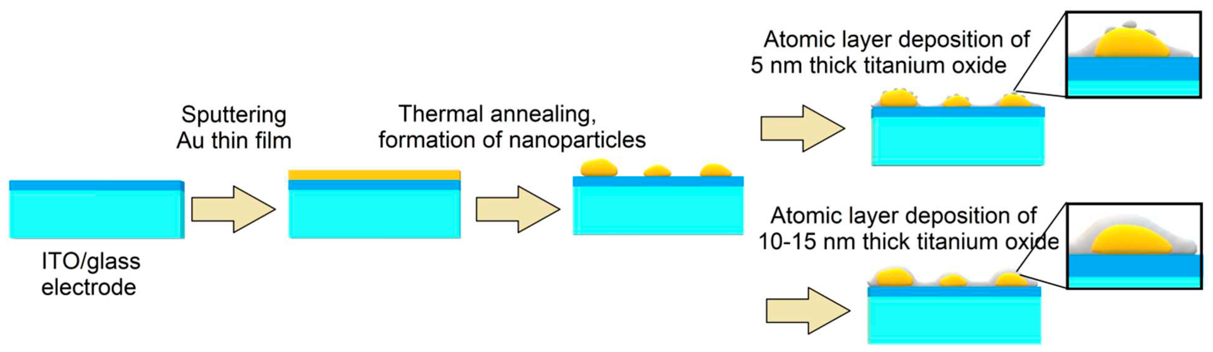
Figure 2.
EDS spectra TiO2 (15 nm)/ITO/glass photoelectrodes (a); Titanium line intensity in spectra with different thicknesses TiO2: 5 nm (b), 10 nm (c), 15 nm (d).
Figure 2.
EDS spectra TiO2 (15 nm)/ITO/glass photoelectrodes (a); Titanium line intensity in spectra with different thicknesses TiO2: 5 nm (b), 10 nm (c), 15 nm (d).
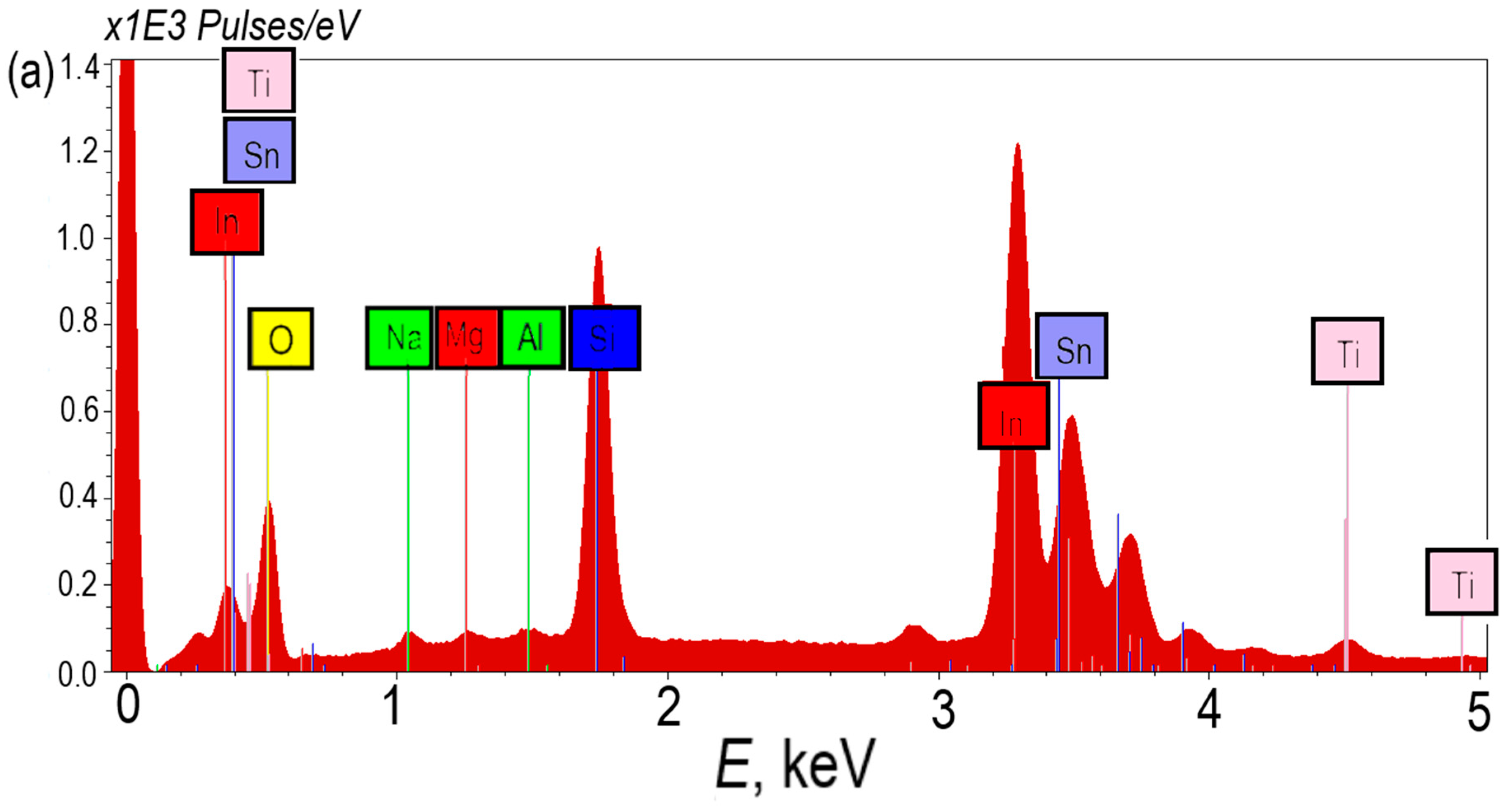
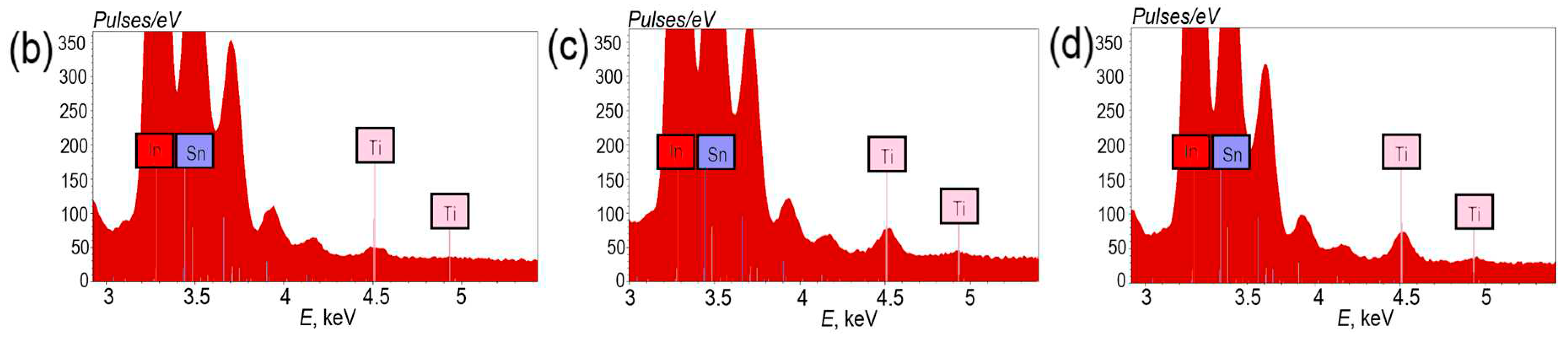
Figure 3.
SEM image of surface TiO2 films, 1-1 (a, d), 1-2 (b, e) и 1-3 (c, f) with ×50k and ×200k magnification.
Figure 3.
SEM image of surface TiO2 films, 1-1 (a, d), 1-2 (b, e) и 1-3 (c, f) with ×50k and ×200k magnification.
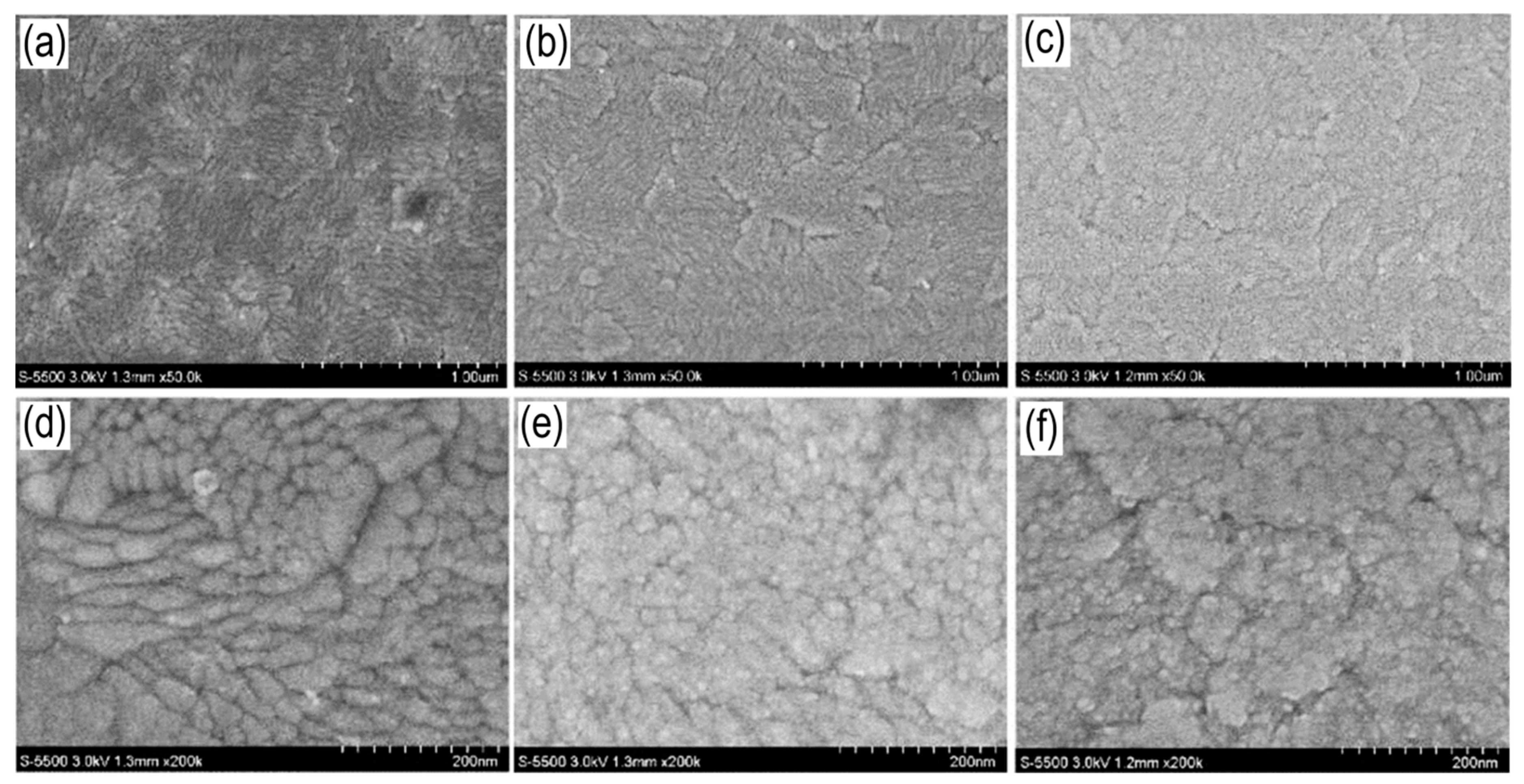
Figure 4.
Spectral transmittance of TiO2/ITO/glass photoelectrodes at different TiO2 thicknesses.
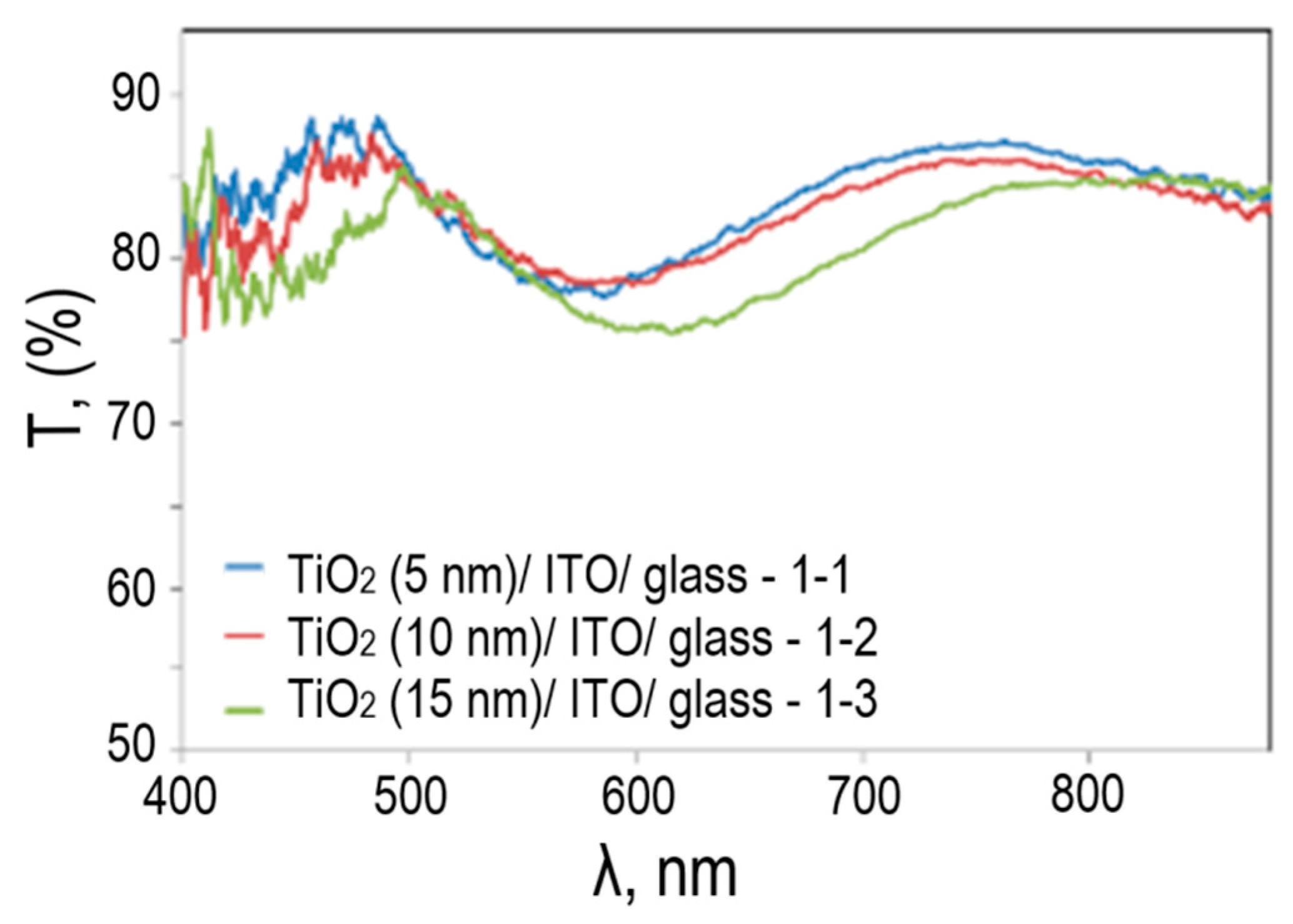
Figure 5.
EDS spectra of TiO2 (15 nm)/Au (5 nm)/ITO/glass photoelectrode (a); EDS spectra of TiO2 (15 nm)/Au (10 nm)/ITO/glass photoelectrode (b).
Figure 5.
EDS spectra of TiO2 (15 nm)/Au (5 nm)/ITO/glass photoelectrode (a); EDS spectra of TiO2 (15 nm)/Au (10 nm)/ITO/glass photoelectrode (b).

Figure 6.
SEM image of the surface of TiO2/Au (5 nm)/ITO composite photoelectrodes, with different TiO2 thicknesses – 2-1 (a, d), 2-2 (b, e) and 2-3 (c, f) with a magnification of ×50 k and ×200 k; TiO2/Au (10 nm)/ITO, with different TiO2 thicknesses – 3-1 (g, j), 3-2 (h, k) and 3-3 (i, l) with an increase of ×50 k and ×200 k; 2-1 (m) and 3-1 (n) with magnification ×400 k.
Figure 6.
SEM image of the surface of TiO2/Au (5 nm)/ITO composite photoelectrodes, with different TiO2 thicknesses – 2-1 (a, d), 2-2 (b, e) and 2-3 (c, f) with a magnification of ×50 k and ×200 k; TiO2/Au (10 nm)/ITO, with different TiO2 thicknesses – 3-1 (g, j), 3-2 (h, k) and 3-3 (i, l) with an increase of ×50 k and ×200 k; 2-1 (m) and 3-1 (n) with magnification ×400 k.
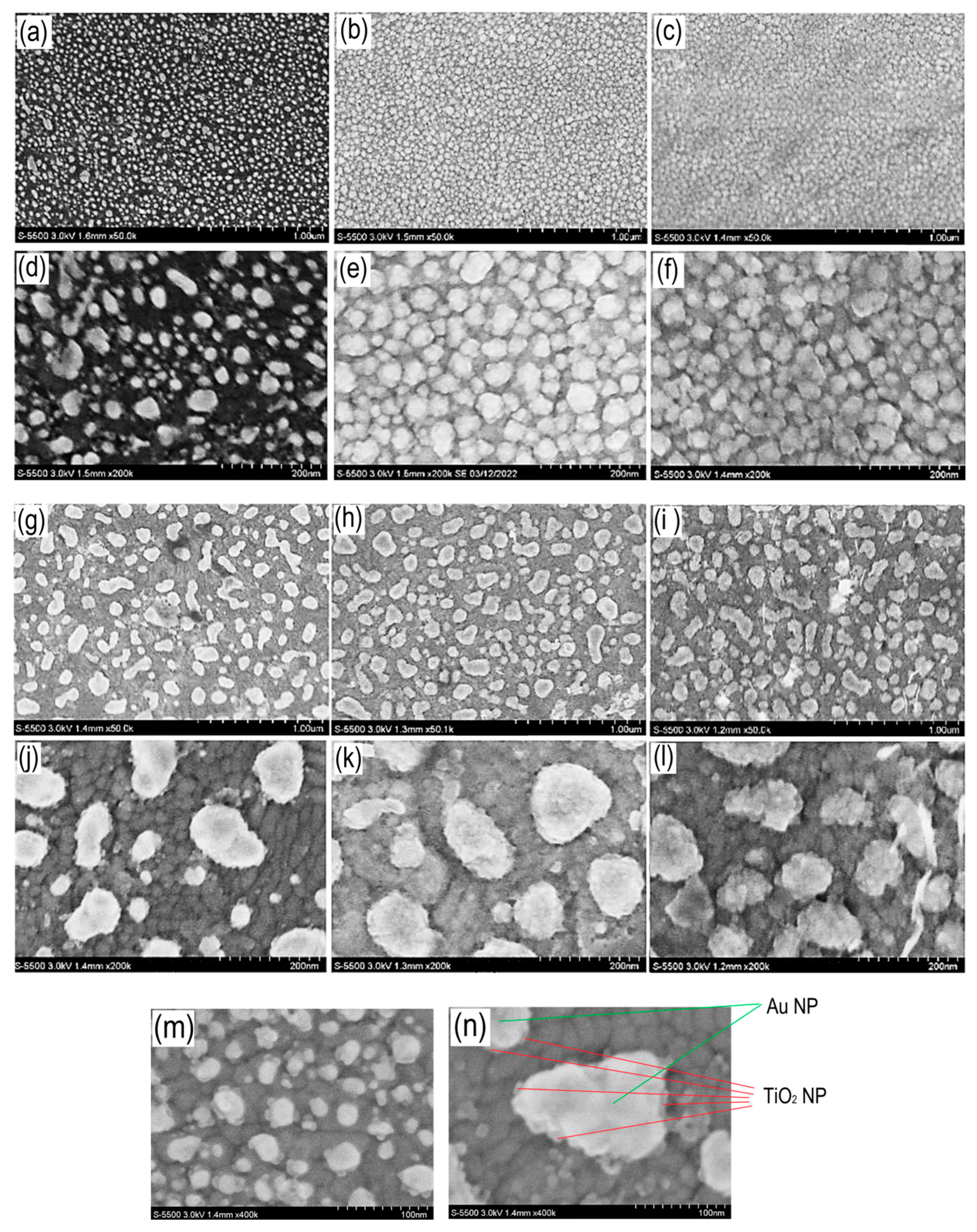
Figure 7.
Spectral transmittance of TiO2/Au (5 nm)/ITO/glass (a) and TiO2/Au (10 nm)/ITO/glass (b).
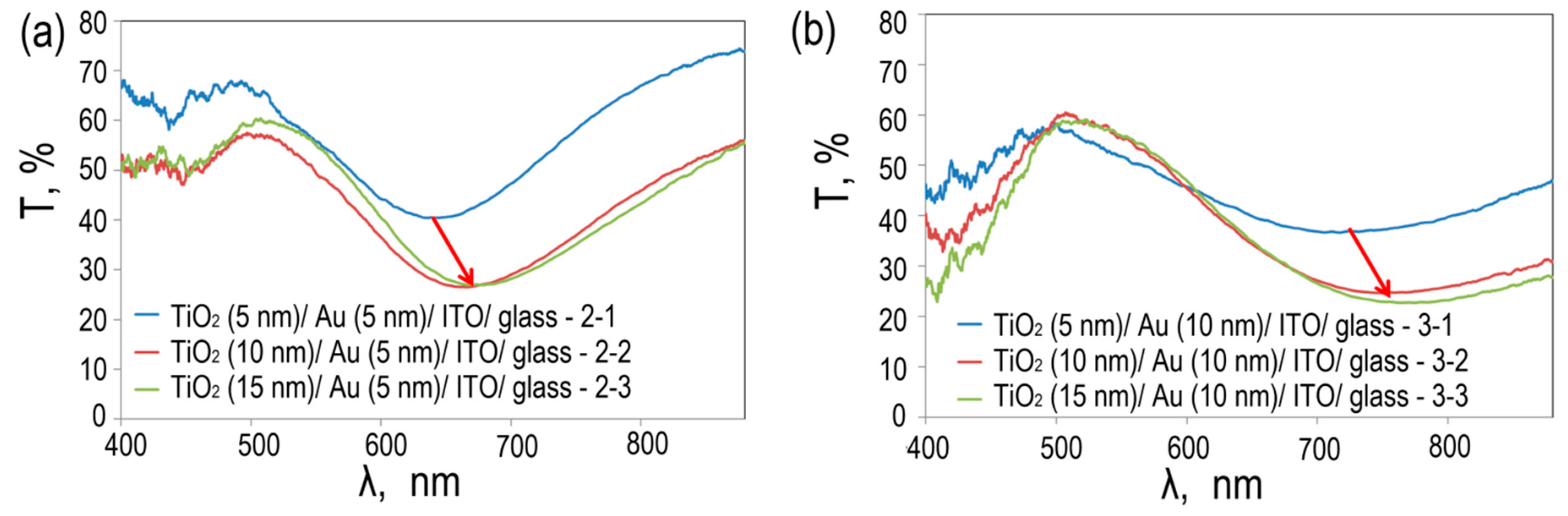
Figure 8.
Cyclic voltammograms of TiO2/ITO/glass photoelectrodes.
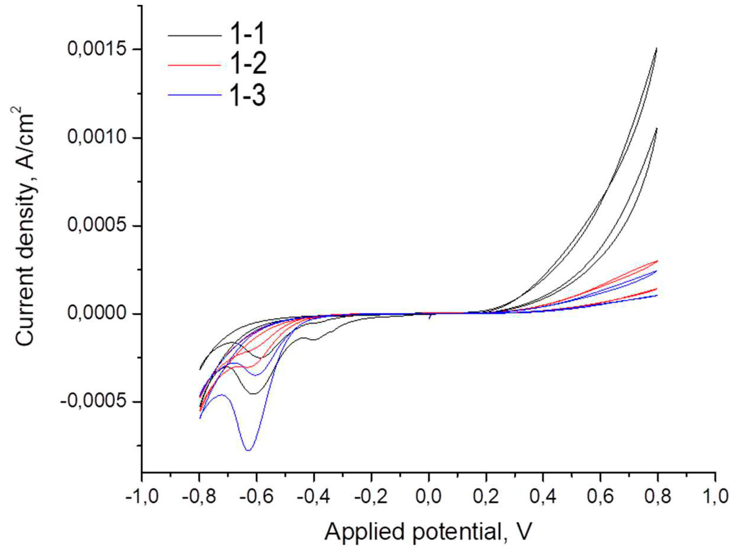
Figure 9.
Equivalent circuit used to simulate the frequency dependences of the impedance of an electrochemical cell (a); Impedance graphs in Bode coordinates for TiO2/ITO/glass photoelectrodes with different thickness of TiO2 layer: 5 nm (b), 10 nm (c), 15 nm (d).
Figure 9.
Equivalent circuit used to simulate the frequency dependences of the impedance of an electrochemical cell (a); Impedance graphs in Bode coordinates for TiO2/ITO/glass photoelectrodes with different thickness of TiO2 layer: 5 nm (b), 10 nm (c), 15 nm (d).
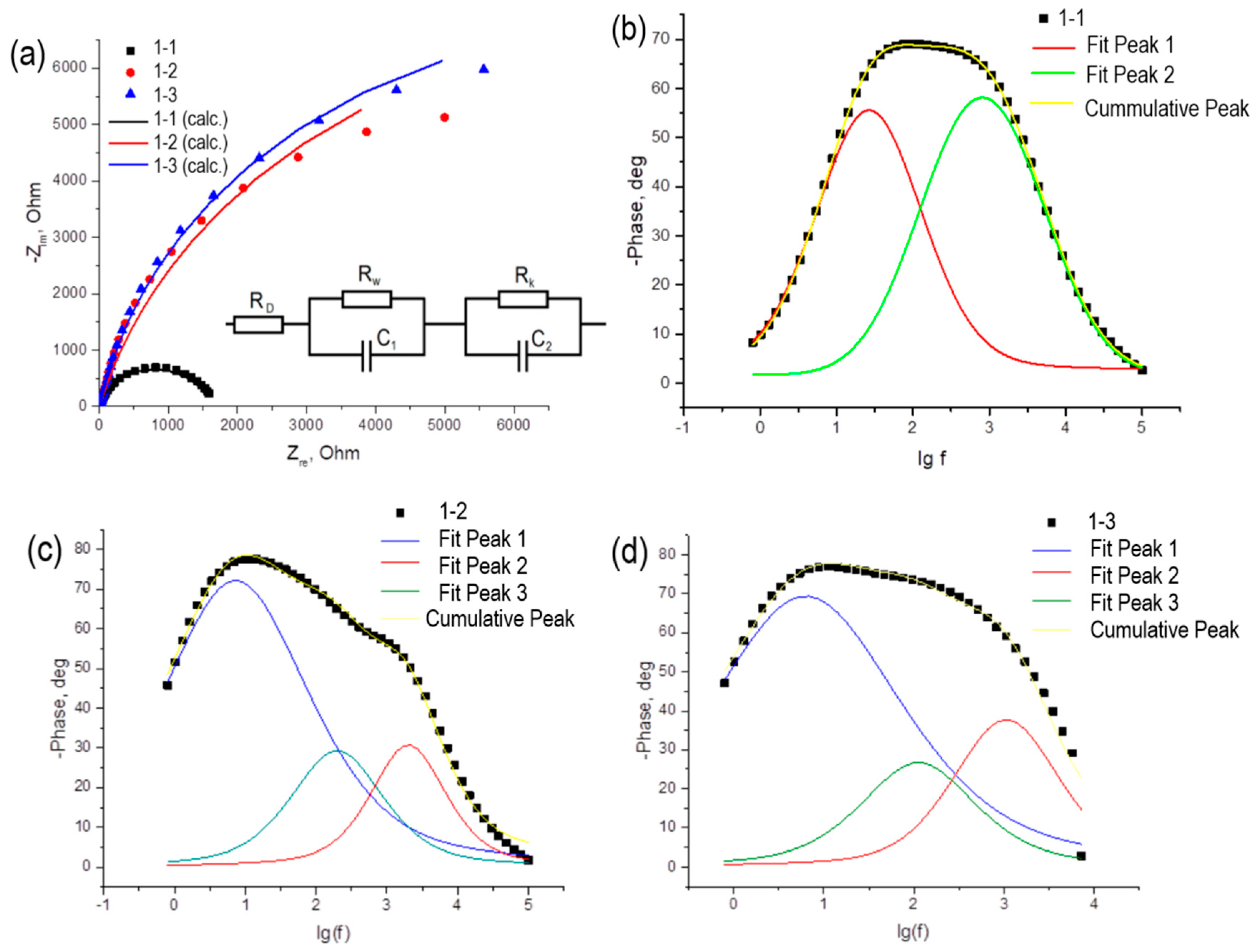
Figure 10.
Cyclic voltammograms of photoelectrodes TiO2/Au (5 nm)/ITO/glass (a) and TiO2/Au (10 nm)/ITO/glass (b).
Figure 10.
Cyclic voltammograms of photoelectrodes TiO2/Au (5 nm)/ITO/glass (a) and TiO2/Au (10 nm)/ITO/glass (b).
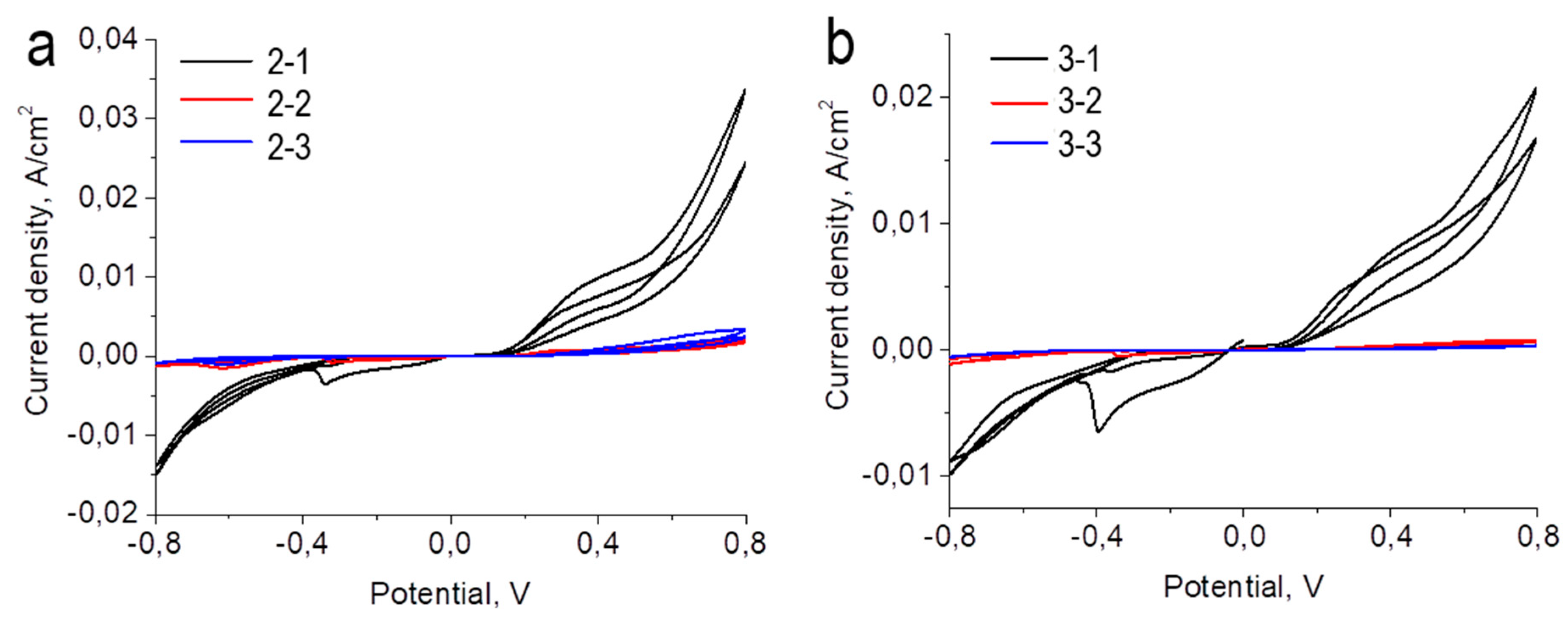
Figure 11.
Equivalent circuit used to simulate the frequency dependences of the impedance of an electrochemical cell for TiO2/Au/ITO/glass photoelectrodes with a different thickness of Au films 5 nm (a) and 10 nm (b); Impedance graphs in Bode coordinates for TiO2/Au/ITO/glass photoelectrodes with a different thickness of Au films 5 nm (c) and 10 nm (d).
Figure 11.
Equivalent circuit used to simulate the frequency dependences of the impedance of an electrochemical cell for TiO2/Au/ITO/glass photoelectrodes with a different thickness of Au films 5 nm (a) and 10 nm (b); Impedance graphs in Bode coordinates for TiO2/Au/ITO/glass photoelectrodes with a different thickness of Au films 5 nm (c) and 10 nm (d).
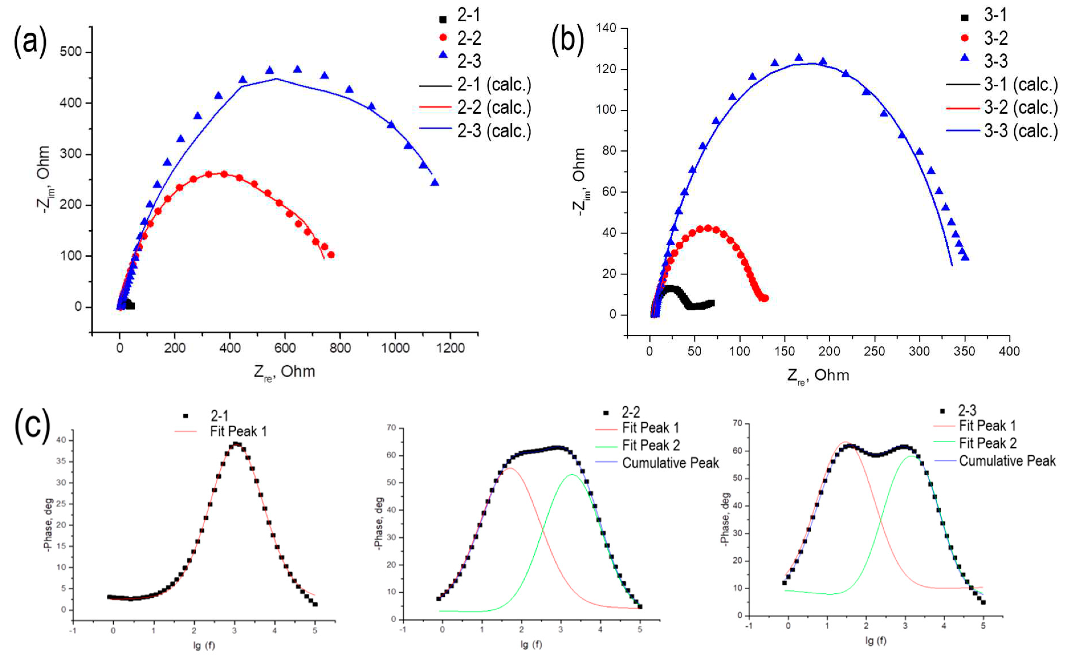
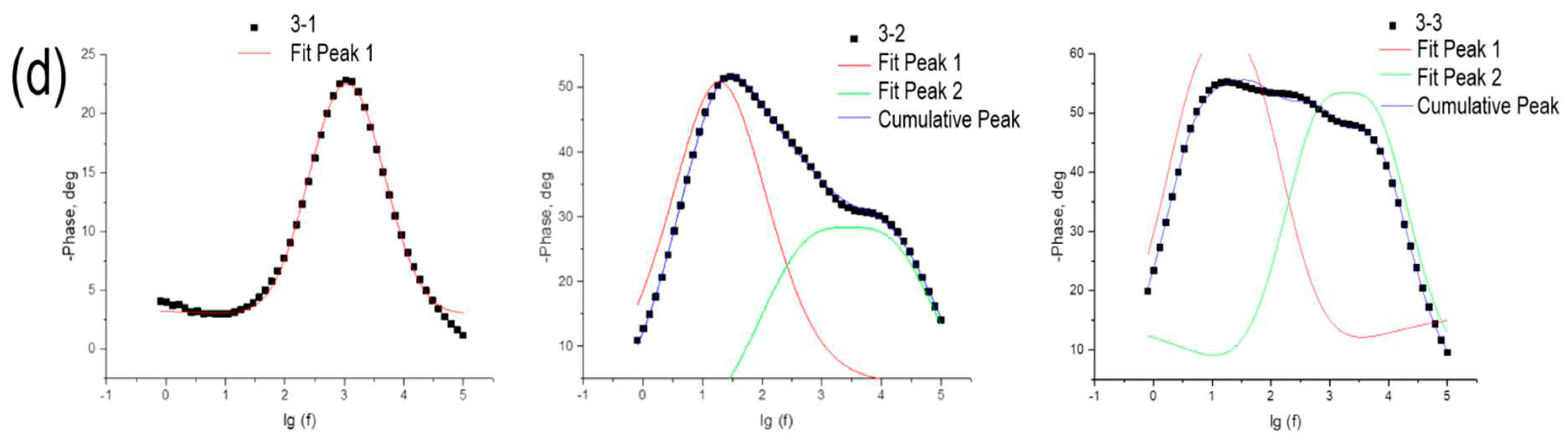

Table 1.
List of photoelectrode series samples TiO2/Au/ITO.
| Sample | TiO2, nm | Au, nm | T, °C |
|---|---|---|---|
| 1-1 | 5 | - | - |
| 1-2 | 10 | - | - |
| 1-3 | 15 | - | - |
| 2-1 | 5 | 5 | 450 |
| 2-2 | 10 | 5 | 450 |
| 2-3 | 15 | 5 | 450 |
| 3-1 | 5 | 10 | 450 |
| 3-2 | 10 | 10 | 450 |
| 3-3 | 15 | 10 | 450 |
Table 2.
Photogalvanic characteristics of TiO2/ITO/glass photoelectrodes.
| Sample | Decoding | Jsc, mA/cm2 | Voc, B | FF, % | η, % |
|---|---|---|---|---|---|
| 1-1 | TiO2 (5 nm)/ITO/glass | 0.005 | 0.132 | 26 | 0.004 |
| 1-2 | TiO2 (10 nm)/ITO/glass | 0.003 | 0.227 | 34 | 0.003 |
| 1-3 | TiO2 (15 nm)/ITO/glass | 0.002 | 0.202 | 43 | 0.002 |
Table 3.
Approximation of data obtained by impedance spectroscopy for a TiO2/ITO/glass photoelectrodes.
Table 3.
Approximation of data obtained by impedance spectroscopy for a TiO2/ITO/glass photoelectrodes.
| Sample | RW, Ohm | RK, Ohm | RD, Ohm |
|---|---|---|---|
| 1-1 | 1592 ± 24 | 140 ± 19 | 4.8 ± 0.1 |
| 1-2 | 16848 ± 2402 | 0.7 ± 0,1 | 6.3 ± 0.2 |
| 1-3 | 15801 ± 1347 | 0.9 ± 0,1 | 9.7 ± 0.2 |
Table 4.
Summary of electrochemical studies for TiO2/ITO/glass photoelectrodes with different TiO2 thicknesses.
Table 4.
Summary of electrochemical studies for TiO2/ITO/glass photoelectrodes with different TiO2 thicknesses.
| Saple | Jsc, mA/cm2 | Lifetimes, ms | N·ε, m-3 | ||||
|---|---|---|---|---|---|---|---|
| τ1 | τ2 | τ3 | 1 | 2 (holes) | 3 | ||
| 1-1 | 0.005 | 6 | 0.2 | 2.5·1019 | 1.0·1019 | ||
| 1-2 | 0.003 | 23 | 0.07 | 0.8 | 8.0·1019 | 1.6·1019 | 2.6·1019 |
| 1-3 | 0.002 | 29 | 0.15 | 1.3 | 1.0·1020 | 1.1·1019 | 2.0·1019 |
Table 5.
Photogalvanic characteristics of TiO2/Au/ITO/glass photoelectrodes.
| Sample | Structure | Jsc, mA/cm2 | Voc,mV | FF, % | η, % |
|---|---|---|---|---|---|
| 2-1 | TiO2 (5 nm)/Au (5 nm)/ITO | 0.036 | 67 | 29 | 0.025 |
| 2-2 | TiO2 (10 nm)/Au (5 nm)/ITO | 0.003 | 80 | 30 | 0.001 |
| 2-3 | TiO2 (15 nm)/Au (5 nm)/ITO | 0.004 | 105 | 23 | 0.002 |
| 3-1 | TiO2 (5 nm)/Au (10 nm)/ITO | 1.123 | 36 | 33 | 0.135 |
| 3-2 | TiO2 (10 nm)/Au (10 nm)/ITO | 0.076 | 20 | 25 | 0.005 |
| 3-3 | TiO2 (15 nm)/Au (10 nm)/ITO | 0.006 | 40 | 26 | 0.001 |
Table 6.
Approximation of data obtained by impedance spectroscopy for a series of TiO2/Au/ITO/glass photoelectrodes.
Table 6.
Approximation of data obtained by impedance spectroscopy for a series of TiO2/Au/ITO/glass photoelectrodes.
| Sample | RW, Ohm | RK, Ohm | RD, Ohm |
|---|---|---|---|
| 2-1 | 1.9 ± 0.5 | 28,9 ± 0,3 | 4.41 ± 0.05 |
| 2-2 | 53 ± 22 | 733 ± 15 | 2.54 ± 0.05 |
| 2-3 | 92 ± 33 | 1220 ± 28 | 3.02 ± 0.09 |
| 3-1 | 39.8 ± 0.5 | 0.11 ± 0.04 | 4.4 ± 0.4 |
| 3-2 | 120 ± 1 | 0.4 ± 0.1 | 4.7 ± 0.3 |
| 3-3 | 340 ± 2 | 0.6 ± 0.1 | 5.4 ± 0.6 |
Table 7.
Summary of electrochemical studies for TiO2/Au/ITO/glass photoelectrodes with different TiO2 and Au thicknesses.
Table 7.
Summary of electrochemical studies for TiO2/Au/ITO/glass photoelectrodes with different TiO2 and Au thicknesses.
| Sample | Jsc, mA/cm2 | Lifetimes, ms | N·ε, M-3 | ||
|---|---|---|---|---|---|
| τ1 | τ2 | 1 | 2 (holes) | ||
| 2-1 | 0.036 | 0.15 | 4.0·1019 | ||
| 2-2 | 0.003 | 3.1 | 0.08 | 8.2·1019 | 9.1·1019 |
| 2-3 | 0.004 | 5.4 | 0.11 | 4.9·1019 | 4.3·1019 |
| 3-1 | 1.123 | 0.15 | 3.1·1017 | ||
| 3-2 | 0.076 | 8.4 | 0.05 | 2.6∙1020 | 6.3·1018 |
| 3-3 | 0.006 | 9.6 | 0.08 | 1.4∙1019 | 1.0·1019 |
Disclaimer/Publisher’s Note: The statements, opinions and data contained in all publications are solely those of the individual author(s) and contributor(s) and not of MDPI and/or the editor(s). MDPI and/or the editor(s) disclaim responsibility for any injury to people or property resulting from any ideas, methods, instructions or products referred to in the content. |
© 2023 by the authors. Licensee MDPI, Basel, Switzerland. This article is an open access article distributed under the terms and conditions of the Creative Commons Attribution (CC BY) license (http://creativecommons.org/licenses/by/4.0/).
Copyright: This open access article is published under a Creative Commons CC BY 4.0 license, which permit the free download, distribution, and reuse, provided that the author and preprint are cited in any reuse.


