
Submitted:
06 December 2023
Posted:
12 December 2023
You are already at the latest version
Abstract
Reliable motor control design is a critical part of the electric vehicle application. Control techniques and motor control devices play an important role in achieving system reliability. In this study, motor control devices have been proposed to implement control techniques in sensorless PMSM. Motor control devices including PWM signal generation by FPGA, gate driver circuit (GDC), and power inverter were developed to be integrated into single-stage motor control devices for sensorless motor control applications. Improvements in GDC design have been the focus to increase the performance of the motor control devices used. Switching losses due to the parasitic elements caused ringing switching behavior of the power inverter circuit, which reduces the performance when the system is integrated. Moreover, in the implementation of sensorless motor control using observer techniques, these conditions affect the accuracy of rotor position estimation, which uses the current or voltage information of the power converter as a variable in the observer design model. Therefore, a GDC design using IR2110 with additional ringing suppression circuit configuration was proposed for the application of motor device control topology to improve the performance of sensorless motor control system. Furthermore, the reduction of switching losses, reduction of current distortion, and accuracy of rotor position information were confirmed by experimental results.
Keywords:
sensorless PMSM
; gate driver circuit
; switching losses
; motor control devices
; estimation of rotor position
1. Introduction
Awareness of environmental issues, including the depletion of natural resources, increasing levels of pollution, significant greenhouse gas emissions, and rising global temperatures, are important motivating factor for considering electric vehicles (EVs) as a viable solution [1,2,3]. On the other hand, various research efforts contributed to technological advances related to the development of EVs used for mobility activities. Control of the electric motor in the EVs drive system is a crucial role to achieve its optimal performance [4]. Therefore, the overall design of the control system must be able to operate reliably, including the control method and motor control devices used [1,2,5]. The motor control method without speed or position sensors (sensorless motor control) is one of the attention of researchers to implement the method in EVs motor control systems [6]. This due to the advantages of the method such as reducing the cost of sensors, simplifying the complexity of the wiring system, and reducing the overall size of the system [7]. In addition, to implement a reliable control system, the motor control device that use should have good performance. In this case, there are three main parts in the device, namely processing digital signal as a generating of signal control, GDC and power inverter [8]. As one of the main parts in the device of motor control application, the GDC is functioned as an interface between control signals and power inverter. Practically, periodic pulse signals or Pulse Width Modulation (PWM) are generated by the processing digital signal such as FPGA, Arduino, LAUNCHXL, and dSPACE. In this case, it should be noted that the signal level of PWM is not capable to drive the gate-to-source terminal of the Insulated Gate Bipolar Transistor (IGBT) or Metal Oxide Semiconductor Field Effect Transistor (MOSFET) directly [9]. Therefore, signal conditioning is required to amplify the signal level as usual. A special set of components and integrated circuits (ICs) are used to perform this important function for signal conditioning, namely regulating the voltage level of the generated PWM accordance with the required gate-to-source threshold voltage level, in this context it referred as GDC. Moreover, the GDC should also be able to provide several protection schemes that require for control device, such as overcurrent (OC), short circuit (SC), and overvoltage (OV) conditions. In the GDC design, that scheme protection referred as isolation systems [4,10]. Furthermore, the GDC system should also be able to minimize switching losses that occur due to the behavior of the power inverter components. So that, in the context of EVs development, reliable gate driver design is also one of the keys to realizing superior performance, high efficiency and optimal operational safety in electric motors. Therefore, good integration between control methods and motor control devices can provide EVs more competitive [1].
Permanent Magnet Synchronous Motor (PMSM) is a type of motor that is popularly used in various fields such as robotics, industrial automation, renewable energy systems and EVs [11,12]. The advantages of PMSM are robust structure, high power density, high efficiency and a wide speed range. The several control techniques were developed and implemented to improve the performance of the motors in various fields, such as EVs [13]. As previously mentioned, sensorless motor control is an alternative for researchers to implement the motor control systems. In general, the application of sensorless motor control techniques can be divided into two categories based on the speed range. The first category shows the motor conditions at standstill to low speed, while the second category is medium speed to high speed. In the first category, the technique utilized the magnetic saliency effect which arises due to the high frequency injection given to the motor [14]. This behavior can be extracted to obtain the rotor position information by several modulation techniques. Meanwhile, for the second category, the technique utilized Back-EMF of the motor. This second technique observed Back-EMF using current or voltage parameters that use to obtain the rotor position information [15]. In this study, the proposed motor control devices were used in the integration of sensorless motor control systems technique that is operated in the second category. In addition, the motor current information is one of the main parameters to determine rotor position information for second category. In PMSM control systems, rotor position information is very important because by this rotor position information, the motor speed can be obtained. Therefore, the feedback for the controller can be used to achieve the results [7].
Based on these various aspects, special attention in designing a motor control system is needed. As mentioned above, GDC design has a vital role in the implementation of motor control systems [16]. Therefore, it is not enough just to be able to provide a good isolation system, but also should be able to minimize switching losses that occur when the whole system is integrated. Switching losses in the power inverter cannot be avoided because the behavior of the semiconductor component itself causes ripples or noise when transitioning from ON to OFF, which is usually called a ringing switching condition [17]. Many researchers have conducted a lot of research on gate driver circuit designs that are implemented in motor control system devices [2,3,5,16,17,18,19]. However, the study of the effect of ringing switching behavior on the application of sensorless motor control systems is still unknown. In general, the design applied in previous research focused on the design of isolated gate driver, active gate driver and high-speed gate driver systems. Therefore, the proposed GDC is designed comprehensively by considering the effect of ringing switching on the power inverter components and providing a good isolation system in the implementation of sensorless control motor devices in this study. The addition of a capacitance filter, resistor bootstrap and snubber circuit has proven to overcome the problem of noise and switching losses in a circuit board design [5,16,18]. However, selecting the best circuit is an important thing to pay attention to effective sensorless motor control devices designed. In this study, the effect of ringing switching conditions on the sensorless motor control system is presented. Briefly, the ringing switching effect have an impact on the accuracy of estimation rotor position in sensorless motor control systems which depend on motor current information. Therefore, the ringing switching effect as a special consideration in designing the proposed system were observed in this study. In addition, cost efficiency in selecting the components has been considered in the proposed control design to ensure appropriate features and a simple configuration. Due to the several important aspects that need to be considered in designing a reliable control system, the main contribution in this study is to provide the motor control devices with improved GDC that are efficient, can minimize switching losses and good isolation system.
The next section of this paper is organized as follows. Section II explained the comparison of gate driver circuits in terms of various criteria. The sensorless PMSM control technique based on Back-EMF estimation was presented in section III. In section IV, the main ideas in the design of the proposed motor control devices were discussed. Furthermore, the experimental results and verification are in section V. Finally, the conclusion was described in section VI.
2. The Comparison of Gate Driver Circuit
GDC design is essential in any application, its reliable performance could improve the performance in the whole system. Based on its application to the motor control device system, GDC is a vital thing to consider for its performance, because its ability to isolate the PWM control signal from the power inverter devices and to perform other additional operations. In general, gate driver ICs and related components for designing GDCs are sold by well-known brands worldwide. However, selecting the right components is considered for the effectiveness of system performance, simple configuration, and cost implications in designing GDCs for motor control system applications. In this study, the implemented control devices in sensorless motor control systems use to drive EVs. Several comparisons are explained to provide an overview of how to determine a reliable GDC. A comparison of GDC design configurations using commonly gate driver ICs is shown in Figure 1.
In [20,21], GDC using TLP250H(F) was applied to a three-level inverter system, where this gate driver was chosen because it has a high driving current, which is suitable as an isolation system between PWM signals and power devices. In addition, the low cost and simple circuit made this gate driver a good choice for efficient GDC designs. The use of the TC4424EPA gate driver was also explained in previous research [2] that is suitable for use in inverters that operate at high frequencies. So that, this type of gate driver is popular for use in SiC, Power IGBT/MOSFET devices that operate over a wide frequency range. In [22], the UCC27710 also has a dual input and output feature that can operate at high voltage and high frequency. So that, it can be an alternative in GDC design for the application of motor drive control systems and smart grid power inverters. As the other component’s IC of GDC types, the IR2110 gate driver is often used in GDC designs. Previous studies [2,5,16,17] have also discussed the application of IR2110 used for motor control systems, isolated gate drivers and high frequency inverters on IGBT/MOSFET power devices with optimal performance.
In addition, a price comparison is also given based on the search results from one of the online vendors as shown in Figure 2. Generally, the unit price of the gate driver IC selected for the proposed system is not the cheapest, but to obtain an effective GDC configuration system with a protection system, good isolation and performance, price efficiency, and the gate driver IC features offered have been considered in determining a reliable and effective GDC design.
Based on the results of the unit price comparison, the IR2110PBF gate driver IC used in the proposed system is the second most expensive. However, considering the system configuration of each gate driver and the provided protection system functions, it is expected that the selected gate driver IC can be the most efficient GDC system design. In this case, the gate driver design using the UCC27710 has the lowest gate driver price. However, there are several important factors to consider when designing a GDC as explained above. In order to design a reliable and safe GDC using the UCC27710 gate driver, it is necessary to add an isolation side to separate the PWM signal ground and the power inverter that increases the cost of the GDC design (Figure 1.c). Furthermore, the gate driver circuit design using the TLP250H(F) has the second cheapest gate driver price (Figure 2), but for application to a motor control system with a half-bridge configuration as shown in Figure 1.b, gate driver components and one circuit are required for signal conditioning in the implementation of motor control systems that operate at high frequencies. Hence, this may increase the price of the GDC design. Meanwhile, the TC4424EPA gate driver has the most expensive price because it has a newer design and features, but this gate driver still requires side isolation and a signal conditioning circuit as shown in Figure 1.a, which increases the complexity and cost of the GDC design. The IR2110PBF gate driver is one of the gate drivers commonly used in motor drive control implementations. As explained in Figure 1.d, the configuration is generally very simple and can be used without adding side isolation because this gate driver is included in the isolated gate driver category as mentioned in previous research [2,17]. In addition, this gate driver IC also does not require the use of signal conditioning even though it operates at high frequency switching, that makes the GDC design more practical. Moreover, to achieve reliable performance in designing the GDC, other comparisons such as delay time and detailed characteristics of each gate driver is considered as shown in Table 1:
Based on the feature’s comparison in Table 1, the IR2110PBF gate driver shows that it has many advantages. Therefore, in this study, this gate driver was selected to improve the GDC design in the proposed motor control device system. In this case, improvements to the GDC design need to be made because considering that the proposed GDC design is not enough to provide good isolation between signal PWM devices and power inverter devices, the GDC design should also provide the best performance in minimizing the resulting switching noise (losses) from the behavior of the system components themselves. Sections IV and V show the effects of switching noise (losses) on the power converter components and the influence of these conditions on the implementation of sensorless motor control systems, where these conditions can reduce the performance and accuracy of the system.
3. A PMSM Mathematical Model for Back-EMF Estimation
Evaluation of the performance of GDC design improvements in the proposed motor device control system was applied to sensorless PMSM motors. Several sensorless motor control techniques have been developed with the aim of increasing the reliability of the use of these motors. In this study, the motor was operated in a wide speed range (medium or high). In general, a popular technique used for the medium to high speed range is Back-EMF estimation using observer technique. The observer technique is a method of estimating a variable that cannot be obtained directly by measurement or observation. In practice, the observer is used to estimate the variable () from the input () and output () because the variable () cannot be obtained directly. In detail, the basic concept of observer technique is shown in Figure 3, there are two main parts, namely the control object and the observer model. In this case, the observer model is designed using parameters from the control object. If the output of the observer model and the control object are the same, the variable () and the estimated variable () will not differ. However, if there is a difference, the error between the output of the control object and the observer model is multiplied by the gain to minimize the error in the estimated variable (), which is the basic principle of the observer technique.
In this study, the full-order state observer is used to obtain Back-EMF estimates. The observer model for Back-EMF estimation is designed using motor parameters (motor resistance (Ra) and motor inductance (La)) and motor variable measurements (voltage or current). In this case, the estimation can be performed because Back-EMF has a correlation in three phase reference frames with speed and rotor position information on the PMSM motor, as shown in Figure 4. For further details, the Back-EMF estimation model for PMSM motors can be formulated in the following equation:
Where are the stator voltage each phase, the stator current each phase, resistance of the armature and self-inductances of the motor respectively, meanwhile p, are differential operator , Back-EMF constant in , and speed of the rotor, respectively. In stationary frame, correlation of Back-EMF in PMSM motor equation can described as follows,
Where ,, , are the stator voltage and current in αβ reference frame, meanwhile and as follows,
In this study, the type of PMSM motor used is a Surface Mounted Permanent Magnet Synchronous Motor (SPMSM). Therefore, the Equation 2 can be rewritten as follows,
Figure 4.
The relationship of rotor position and speed of the motor in three reference frames.
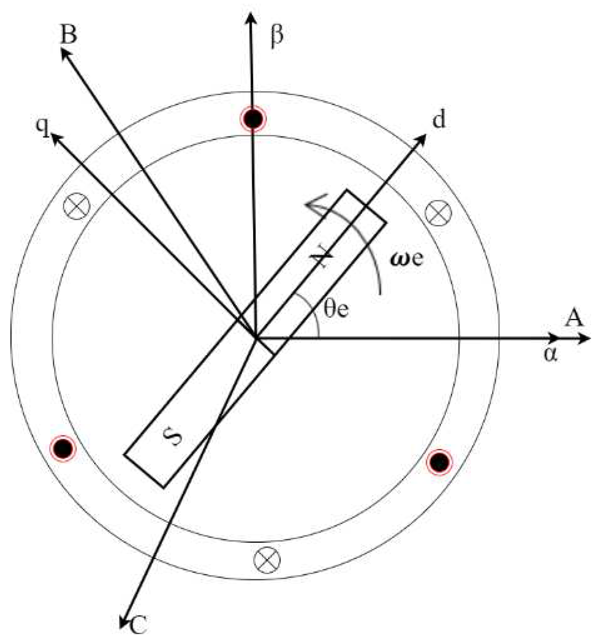
According to the correlation shown in Figure 4 and Equation 2, the rotor position and motor speed information can be known. In addition, the control object and observer equation of this study are described as follows,
The output difference between the control object and the observer model can be written as the following error equation,
According to Equation 5, the Back-EMF estimation in the full-order observer was implemented using alpha-beta current information ( and the gain vector can represented by the matrix when the Back-EMF axis are assumed as follows,
In this study, based on the observer result, the estimated rotor position and rotor speed can be expressed by the following equation:
Where , , , are estimated position of rotor, speed estimation of the rotor, Back-EMF in alpha (α) axis and Back-EMF in beta (β) axis, respectively. In this case, the design of the observer model is highly dependent on the current signal to be obtained Back-EMF estimated. Therefore, minimizing the interference or noise in the signal can maintain the accuracy of rotor position estimation. The effect of current signal distortion on the performance of rotor position estimation in sensorless PMSM motor control systems is discussed in detail in section V.
4. Proposed Devices for otor Control Application
This section explains in detail the system integration in improving the implementation of sensorless motor control devices. In this study, the proposed configuration of single-stage motor control devices includes the improvement GDC using IC IR2110PBF with ringing suppression circuit, PWM signal generation using FPGA, and power inverter using IGBT FGW85N60RB. The proposed system aims to provide a good isolation side, minimize switching losses and suitable for implementation in sensorless motor control systems. The overall schematic of the proposed system is shown in Figure 5.
Figure 6 shows the results of the proposed prototype laboratory motor controller. The PWM signal generated by the FPGA has a voltage level of 3.3V with limited current capability, so it cannot be used to directly drive the IGBT inverter. Therefore, conditioning the PWM signal level and providing good side isolation is the first focus in our proposed system. The FOD 3182 optocoupler IC is used to amplify the signal and provide isolation functions in the GDC design. This IC could increase the PWM signal level to 15V with a current capability of up to 1A and also can provide good isolation conditions. The amplified and isolated PWM signal is then applied to the IR2110PBF gate driver IC to generate high and low side signals that are used to drive the IGBT on the inverter component. In the contrary from previous studies and typical configuration, the GDC using the IR2110PBF usually requires two power supplies because the voltage levels on the input and output sides have different voltage levels. However, in the proposed system, the input and output voltage levels are same by voltage amplification, so that one power supply is sufficient. In addition, there is an indicator that shows whether PWM is active or non- active to facilitate the analysis process when troubleshooting is required.
Furthermore, by selecting the proper RG, maximum current can be drawn from the GDC to quickly charge the capacitance gate of the Ciss (CGD+ CGS+ CDS) power inverter component when it is on. The fast recovery diode FR207 and RPD are used during the OFF state to provide system safety against floating gate conditions when the power inverter component is not activated (Coss discharge including IF). On the other hand, the second focus in our proposed systems to minimize switching losses due to ringing switching behavior in the power inverter component. So that, it is necessary to add a circuit to overcome this in the proposed GDC design configuration. The equivalent circuit in Figure 7 describes the flow analysis of the ringing condition, including parasitic elements in the power switching component. CGD, CGS, CDS, LD, LG, LS are capacitance and inductance represent parasitic element of gate, drain and source in power switching component. While, Ra, La, ea are resistance of PMSM, inductance of PMSM, induced voltage of PMSM, respectively.
In this system, the parasitic inductance in the ringing flow appeared with the notation LPS as a parasitic element on the source side when the DC source and Cin are connected. In addition, RPS appeared as AC and DC resistance in the ringing flow area. Parasitic inductance was connected in series with the drain and source in the power switching component that has impact on the transition speed and peak voltage connected to the load. The voltage across the parasitic inductor during the ON-to-OFF transition or vice versa can be explained using Equation 18. During the ON transition, the ID drain output current increases and produces a positive voltage due to the effect of crossing the parasitic inductance, which causes a decrease in the effective voltage on the power switching device by inducing the occurrence of a voltage spike on the negative side. Meanwhile, during the OFF transition, the ID output current decreases and produces a negative voltage due to the effect of crossing the parasitic inductance, which causes a voltage spike to be induced on the positive side. Based on these conditions, a C filter circuit and ringing suppression can be added to reduce the effect of parasitic inductance (LP + LPS), which increases significantly in high frequency system implementations. The effect of parasitic inductance was represented in a ringing condition flow equivalent circuit for circuit analysis. In this study, the flow and load equivalent circuit in the GDC design using IR2110PBF included a typical configuration, a configuration with the addition of a filter, and a proposed configuration with the addition of a ringing suppression circuit shown in Figure 8. In the condition of the voltage at Cin and source was constant, the drain-to-source voltage can reach its peak with the drain output current value ID approaching 0. In addition, if the input voltage at capacitor Cin is less than the source voltage due to parasitic effects and the output capacitor voltage Coss is greater, ringing current condition can be occurred as shown in the blue dashed line. The filter C and the ringing suppression circuit role to provide a path by bypassing the resonance phenomena caused by parasitic elements. Hence, the circuit minimized the effects of parasitic elements at high frequencies and prevented high-frequency currents from returning to the source. Therefore, attenuation can be achieved in ringing flow conditions.
In addition, the GDC design using the IR2110PBF IC gate driver by applying a typical configuration, a configuration with the addition of a filter circuit, and a proposed configuration with the addition of a ringing suppression circuit were observed to obtain reliable GDC design improvements in the implementation of the proposed motor control devices. The three schematic diagrams of each configuration are shown in Figure 9.
The results of testing the ringing switching conditions of power switching components in previous research were used to see the presence of parasitic phenomena under these conditions. Based on these observation results (Figure 10b and Figure 10c), the use of capacitors as a filter circuit installed in parallel on the high and low sides is proven to minimize the ringing switching conditions up to 75% in the PWM signal of power inverter compared to typical configuration. However, it is necessary to improve the effectiveness of minimizing these conditions to achieve better performance.
The result of the proposed configuration using a ringing suppression circuit appears to have superior performance effectiveness in minimizing switching losses at the GDC output (Figure 10d). In this study, when the voltage spike occurs, it does not exceed 1.75% of the nominal PWM voltage. Therefore, in the proposed GDC configuration, a ringing suppression circuit was implemented using a series-parallel circuit of capacitor and resistors connected to the load. Practically, the equation for determining the capacitance and resistance values of the ringing suppression circuit according to the equivalent circuit analysis in Figure 8c can be written by the several equations in the following:
The voltage spike during transition condition including the parasitic effect can be described as follows,
Due to the inductance parasitic effect which caused resonant condition occurs. Hence, this condition can be written as follows,
The assumed of voltage spike and resonant condition impact of parasitic inductance effect can be analyzed by adding the capacitor and damping resistor. Therefore, the inductance parasitic elements of the circuit can be calculated by following equation:
In addition, the ringing flow was occurred when the switch is closed and a voltage source is connected to a series LC configuration of the parasitic element. Furthermore, to consider the damping ratio and frequency that use for the circuit, the capacitance and resistance value of the ringing switching circuit can be described as follows,
Where are peak spike voltage in ringing switching behavior, voltage in inductance parasitic, drain current, floating current in OFF condition, respectively. Meanwhile, are spike resonant in ringing flow, frequency value of ringing flow by original capacitance effect in semiconductor component, resonant value of ringing flow by original capacitance effect in semiconductor component with additional external capacitance, switching frequency respectively. Furthermore, , ξ are inductance in parasitic behavior, capacitance of ringing suppression circuit, original capacitance value in semiconductor component, external capacitance to show effect parasitic in ringing flow, resistance of ringing suppression circuit, resistance of pulldown and OFF condition, damping in optimal design of ringing suppression circuit, respectively.
Based on the above explanation, the effectiveness of GDC performance can be increased by minimizing switching losses caused by the ringing switching behavior of semiconductor components. This is an important factor in achieving reliable motor control performance. The evaluation of the proposed motor control device in the implementation of a sensorless motor control system is explained in the next section.
5. Experimental Results
In order to evaluate the practical performance of the proposed laboratory prototype motor control device design, the experimental setup is shown in Figure 11. Tests were conducted on the implementation of PMSM sensorless motor control using the Back-EMF estimation by observer method to obtain information on the rotor position and motor speed. In this study, the motor was operated in the speed range of 1000 rpm to 3000 rpm, in which the Back-EMF estimation could be well performed. Two current sensors are installed in phase A and phase B as a variable information to design the observer model for the Back-EMF estimation process. In this case, the results of the current sensor readings for each phase were processed by the ADC and DAC system and displayed on the Memory Hi-Corder to simplify the evaluation and analysis process performed. Detailed specifications of the supporting equipment used in the experimental setup are explained in Table 2.
The experimental comparison results are detailed in Table 3. Several tests were performed on the proposed motor controller device with a switching frequency of 25 kHz. The first test was conducted on the integration of the sensorless PMSMS motor control system with the motor controller device using a typical GDC IR2110PBF configuration (Figure 9a). In this study, the system performance evaluation regarding the ringing switching behavior during the transition condition from OFF to ON is observed, because direct impact on the performance of the motor device control system. Figure 12 shows that the inverter output current waveform connected to the motor experiences an average current spike of more than 33%, which is more than 1 ampere in the peak current conditions of 3A. In this case, this condition occurs for 4ms in one cycle period. These results show that the parasitic effect on the power inverter component as mentioned earlier, caused the ringing switching loop phenomenon that impact the inverter PWM waveform (Figure 10b).
In this study, reported there are correlation with the current spike that occurs at the inverter output due to effect resonant and voltage spike in PWM. According to the results (Figure 12a and Figure 12b), it is known that the current waves in phase-A and phase-B are distorted, which affects the performance of the Back-EMF observer that requires motor current information. Hence, the condition causes the rotor position estimation to be disturbed, thereby reducing the accuracy of the observer to estimate the rotor position (Figure 12c). Therefore, this problem should be avoided when implementing a sensorless motor control system.
The GDC configuration with the addition of capacitor components in each section of the high and low side gate drivers (Figure 9b) was implemented in the second motor device control test. This is intended to minimize spikes in the PWM inverter (Figure 10c). However, based on the results shown in Figure 13, the effectiveness performance of the motor controllers was still less than optimal because the current distortion in phase-A and phase-B was still quite large about 30% in the peak current conditions of 3A (Figure 13a and Figure 13b). Although the spike oscillation time in this condition is 2ms shorter than the first test, this condition still has an impact on reducing the accuracy of the rotor position estimation results (Figure 13c). Therefore, efforts to minimize the occurrence of spikes are still needed to improve the performance of motor controllers.
The third test was performed on an improved GDC configuration using a ringing suppression circuit to minimize the spikes that occurred. In this study, this configuration (Figure 9c) was applied to control motor devices proposed in the implementation of a sensorless PMSM motor control system. In Figure 14, the effectiveness of the proposed system showed good performance. In this case, when the output current inverter connected to motor is 3A the voltage spike on the PWM to drive the IGBT power inverter can be properly minimized (Figure 10d). Based on the test results shown in Figure 14a and Figure 14b, the current waveform is consistently smoother. In the event of a current spike, the maximum does not exceed 10% of the peak current of 3A and the oscillation time is approximately less than 1ms. Moreover, minimizing the current distortion in phase-A and phase-B can maintain the accuracy of the rotor position estimation, as depicted in Figure 14c.
In addition, the test taken by different current has been carried out to show that the performance of the proposed system is not dependent on the current used. The peak current of the inverter connected to the motor was raised to 4A. The results in Figure 15a and Figure 15b seem there is no current spike and the waveform also consistently smoother. So that, the result of estimation rotor position using Back-EMF observer shown performance is well to obtained the rotor position information (Figure 15c).
It should be noted that spikes, which cause distortion of the motor current, are caused by the ringing switching behavior impact of the resonance parasitic elements in inverter components, as well as electromagnetic interference (EMI). This condition expected not only affects the accuracy of rotor position estimation, but also increases total harmonic distortion (THD) and reduces power efficiency due to potential electrical losses. As explained earlier, the ringing switching behavior was caused by the components in the inverter. Therefore, it is expected that the proposed motor control device design with the addition of a ringing suppression circuit to the IR2110PBF gate driver IC configuration can also be implemented and function well with other types of gate driver ICs. Thus, the design of the proposed system can be effectively used in the application of sensorless motor control systems to improve performance, enhance the accuracy of rotor position estimation, and reduce electrical system losses that can negatively affect the overall system performance.
6. Conclusions
In this study, an optimal control motor device by improvement GDC has been proposed for the implementation of sensorless PMSM motor control. The evaluation based on experimental and theoretical aspects showed that the improvements in the proposed GDC were proven to reduce the switching losses in semiconductor materials and EMI in circuit designs. The switching losses caused by ringing condition in the effect of parasitic element, gave the effect of periodic current distortion, which can reduce the performance of motor control devices. On the other hand, this study also evaluated the ringing switching condition had an impact on the accuracy of estimating rotor position by back-EMF observer of a sensorless motor control system, which uses current information to extract rotor position information. From the results of the experiments, it is confirmed that the proposed systems can overcome these two problems by producing low switching losses and eliminating current distortion to obtain accurately estimation of rotor position. In summary, the improvement of GDC has demonstrated the performance of cost-effective implementation of sensorless motor control systems. Moreover, the proposed systems and its design methodology should serve as a roadmap for beginners in developing reliable power electronic systems, especially in motor control implementation. In the future study, the application of the proposed systems to sensorless PMSM motor control using other techniques such as high-frequency injection will be conducted.
References
- Li, A; Yuan, W; Li, S; Wang, X; Qiu, X; Xu, L. Design and Implementation of Controller for EHPS of Intelligent Electric Bus. IEEE Access. 2019,7, 89400-89411. [CrossRef]
- Tomar, P.S; Sandeep, N; Verma, A.K; Srivastava, M. Analysis, design, and implementation of an improved gate driver for high switching frequency EV application. IET Power Electronics. 2020,13,1797-1806. [CrossRef]
- Santra, S.B; Roy, A; Chatterjee, D. Design of Bootstrap Capacitor Based GaN-FET driver for Improvement in Transient Performance of DC-DC Converter. In Proceedings of the 2020 IEEE International Conference on Power Electronics, Smart Grid and Renewable Energy (PESGRE2020), Cochin, India,2-4 June 2020; pp. 1-6.
- Yin, S; Tseng, K.J; Tu, P; Simanjorang, R; Gupta, A.K. Design Considerations and Comparison of High-speed Gate Drivers for Si IGBT and SiC MOSFET Modules. In Proceedings of the 2016 IEEE Energy Conversion Congress and Exposition (ECCE), Milwaukee, WI, USA, 18-22 Sept 2016; pp. 1-8.
- Barman, P; Baruah, P; Sharma, S. An Optoisolator Based Gate Driver Design for Reliable Operation in High Power Motor Control Applications. In Proceedings of the 2021 International Conference on Advances in Electrical, Computing, Communication and Sustainable Technologies (ICAECT),Bhilai, India, 19-20 Feb 2021; pp.1-6.
- Yang, W; Guo, H; Sun, X; Riaz, S; Zaman, H. Wide-Speed-Range Sensorless Control of IPMSM. Electronics, 2022,11, 1-19. [CrossRef]
- Wang, G; Valla, M; Solsona, J. Position Sensorless Permanent Magnet Synchronous Machine Drives—A Review. IEEE Transactions on Industrial Electronics. 2019,67, 5830 - 5842. [CrossRef]
- Peftitsis, D; Rabkowski, J. Gate and Base Drivers for Silicon Carbide Power Transistors: An Overview. IEEE Transactions on Power Electronics. 2016, 31, 7194-7213. [CrossRef]
- Yin, S; Tseng, K.J; Simanjorang, R; Tu, P. Experimental comparison of high-speed gate driver design for 1.2-kV/120-A Si IGBT and SiC MOSFET modules. IET Power Electronic. 2017, 10, 979-986. [CrossRef]
- Yamaguchi, K; Katsura, K; Yamada, T; Sato, Y. Comprehensive Study on Gate Driver for SiC-MOSFETs with Gate Boost. IEEJ Journal of Industry Applications. 2017, 7, 218-228. [CrossRef]
- Huang, Y; Zhao, M; Wang, Y; Zhang, H; Lu, M. An Improved Full-Speed Domain Sensorless Control Scheme for Permanent Magnet Synchronous Motor Based on Hybrid Position Observer and Disturbance Rejection Optimization. Electronics. 2023, 12, 3759, 1-21. [CrossRef]
- Sieklucki, G; Kara, D. Design and Modelling of Energy Conversion with the Two-Region Torque Control of a PMSM in an EV Powertrain. Energies, 2022, 15, 4887, 1-18. [CrossRef]
- Aiso, K; Akatsu, K. Performance Comparison of High-Speed Motors for Electric Vehicle. World Electric Vehicle Journal, 2022, 13,57, 1-17. [CrossRef]
- Wang, S; Yang, K; Chen, K. An Improved Position-Sensorless Control Method at Low Speed for PMSM Based on High-Frequency Signal Injection into a Rotating Reference Frame. IEEE Access. 2019, 77, 86510-86521. [CrossRef]
- Zhang, Z. Sensorless Back-EMF Based Control of Synchronous PM and Reluctance Motor Drives—A Review. IEEE Transactions on Power Electronics. 2022, 37, 10290-10305. [CrossRef]
- Anuragh, N; Nath, S. Effect of Optocoupler Gate Drivers on SiC MOSFET. In Proceedings of the 2021 National Power Electronics Conference (NPEC), Bhubaneswar, India, 15-17 Dec 2021; pp.1-6.
- Zhou, Z; Li, Z; Rao, J; Jiang, S; Sakugawa, T. A High-Performance Drive Circuit for All Solid-State Marx Generator. IEEE Transactions on Plasma Science. 2016, 44, 2779-2784. [CrossRef]
- Yatsugi, K; Nomura, K; Hatori, Y. Analytical Technique for Designing an RC Snubber Circuit for Ringing Suppression in a Phase-leg Configuration. IEEE Transactions on Power Electronics, 2017, 33, 4736-4745. [CrossRef]
- Jin, W; Cho, K. A Supply Voltage Noise Immunity Enhancement Design for High-Voltage Gate Driver IC based on Bootstrap Circuit. IEEE Transactions on Circuits and Systems II: Express Briefs, 2021, 68, 3048-3052. [CrossRef]
- Hamed, H.A; Al-Mansori, F.N. An effective IGBT driver circuit for three level neutral point clamped converters. Int. J. Industrial Electronics and Drives. 2018, 4, 25-31. [CrossRef]
- Palanisamy. R; Vijayakumar, K. Hardware Implementation of Single-Phase Diode Clamped 3-Level Inverter. International Journal of Control Theory and Applications.2016, 9, 975-981.
- UCC2710, 620V, 0.5 A, High Side- Low Side Gate Driver, Texas Instrument, 2018.
- Optocoupler High-Speed MOSFET Drivers TLP250H/250HF, Toshiba corporation, 2015.
- 3A Dual High-Speed Power MOSFET Drivers TC4423/TC4424/TC4425, Microchip Technology Inc, 2012.
- High and Low Side Driver, IR2110(S)PbF/IR2113(S)PbF, PD60147 rev.V, Infineon 2019.
- Zhang, Z; Guo, B; Wang, F. Evaluation of Switching Loss Contributed by Parasitic Ringing for Fast Switching Wide Band-Gap Devices. IEEE Transactions on Power Electronics. 2019, 34, 9082-9094. [CrossRef]
Figure 1.
The configuration of Gate Driver Circuit: (a) Configuration by TC442EPA; (b) Configuration by TLP 250(H)F; (c) Configuration by UCC27710; (d) Configuration by IR2110PBF.
Figure 1.
The configuration of Gate Driver Circuit: (a) Configuration by TC442EPA; (b) Configuration by TLP 250(H)F; (c) Configuration by UCC27710; (d) Configuration by IR2110PBF.
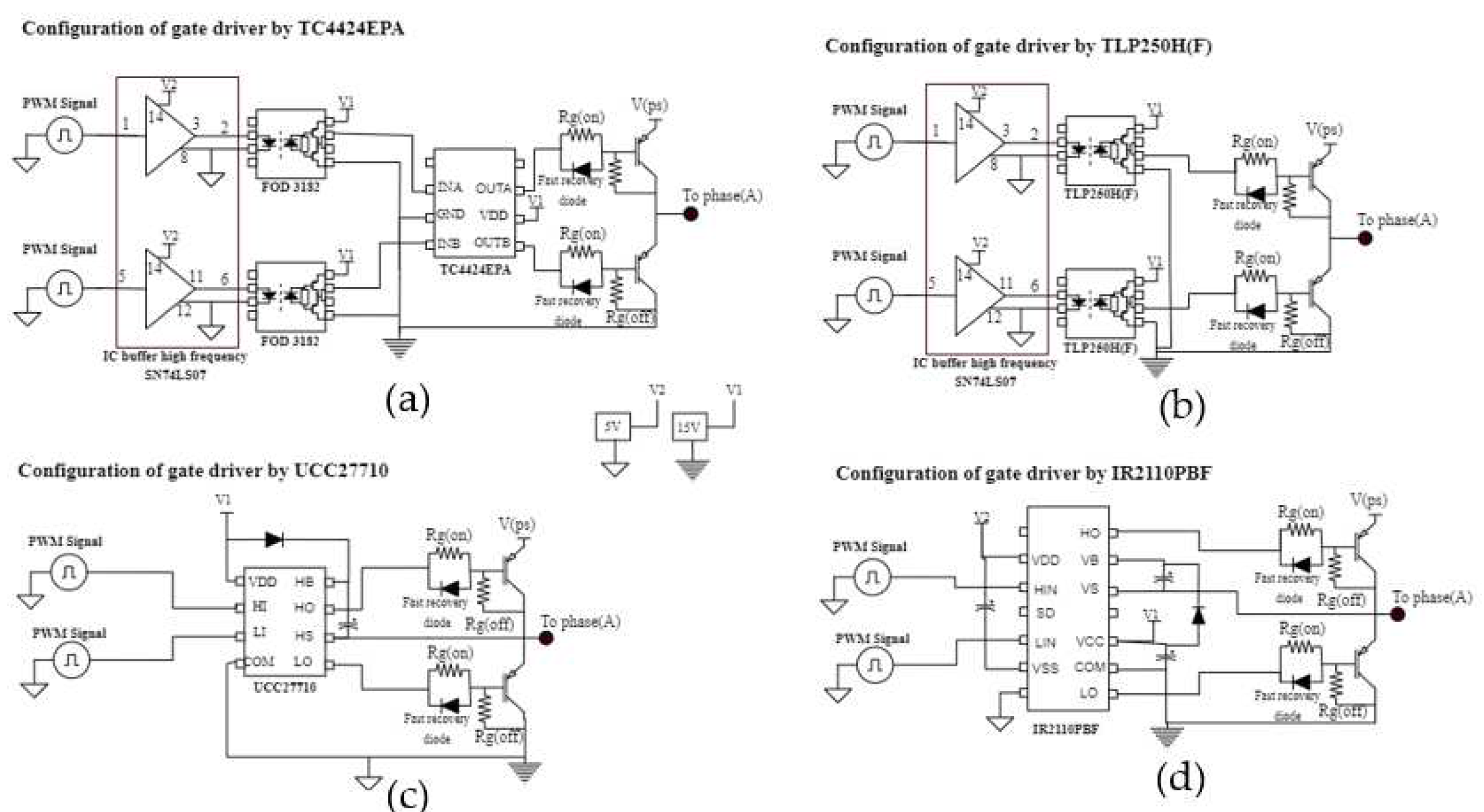
Figure 2.
The comparison price per-unit of gate drivers. (Note: Prices shown are subject to market fluctuations.).
Figure 2.
The comparison price per-unit of gate drivers. (Note: Prices shown are subject to market fluctuations.).
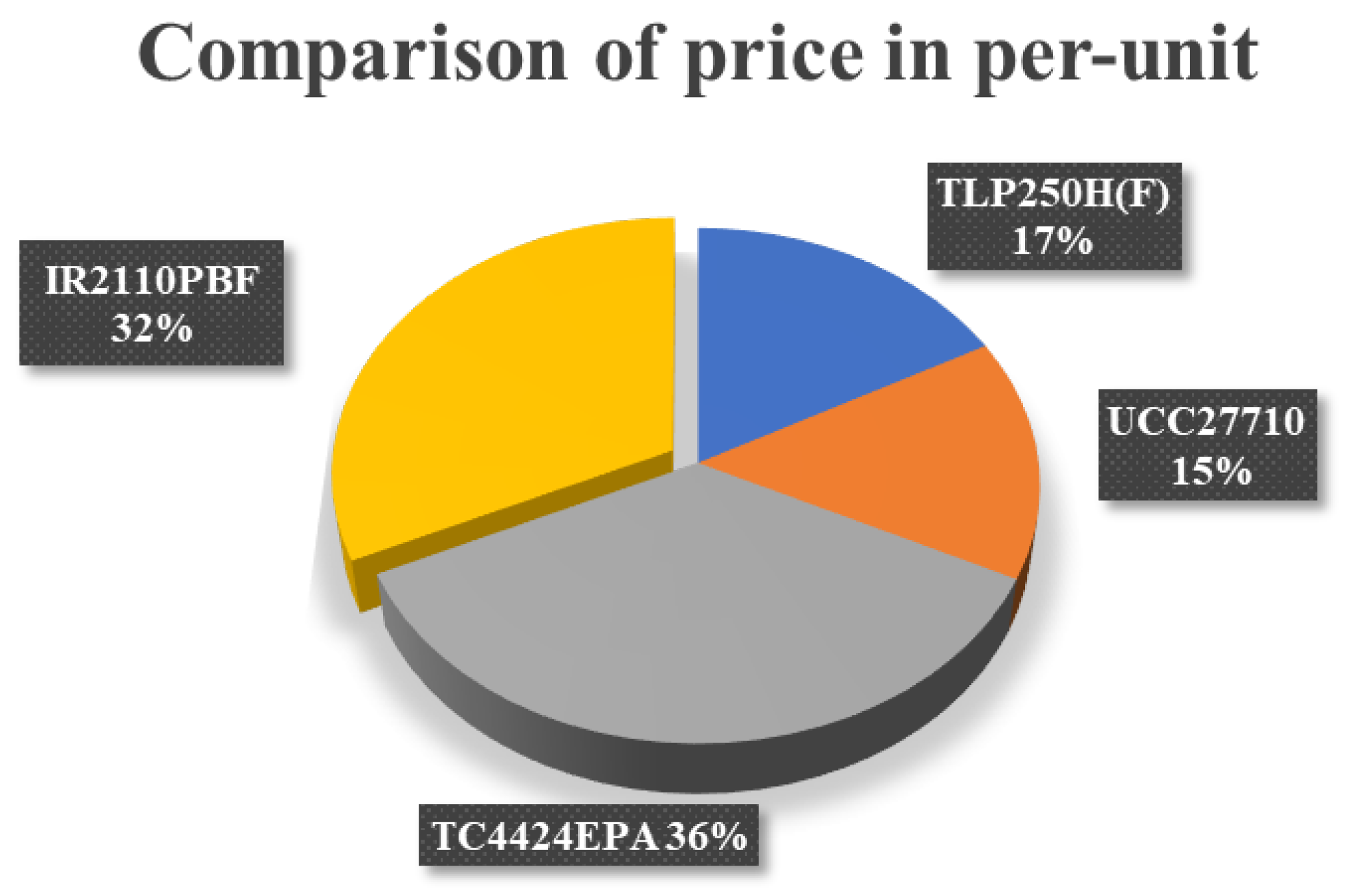
Figure 3.
Full-order state observer.
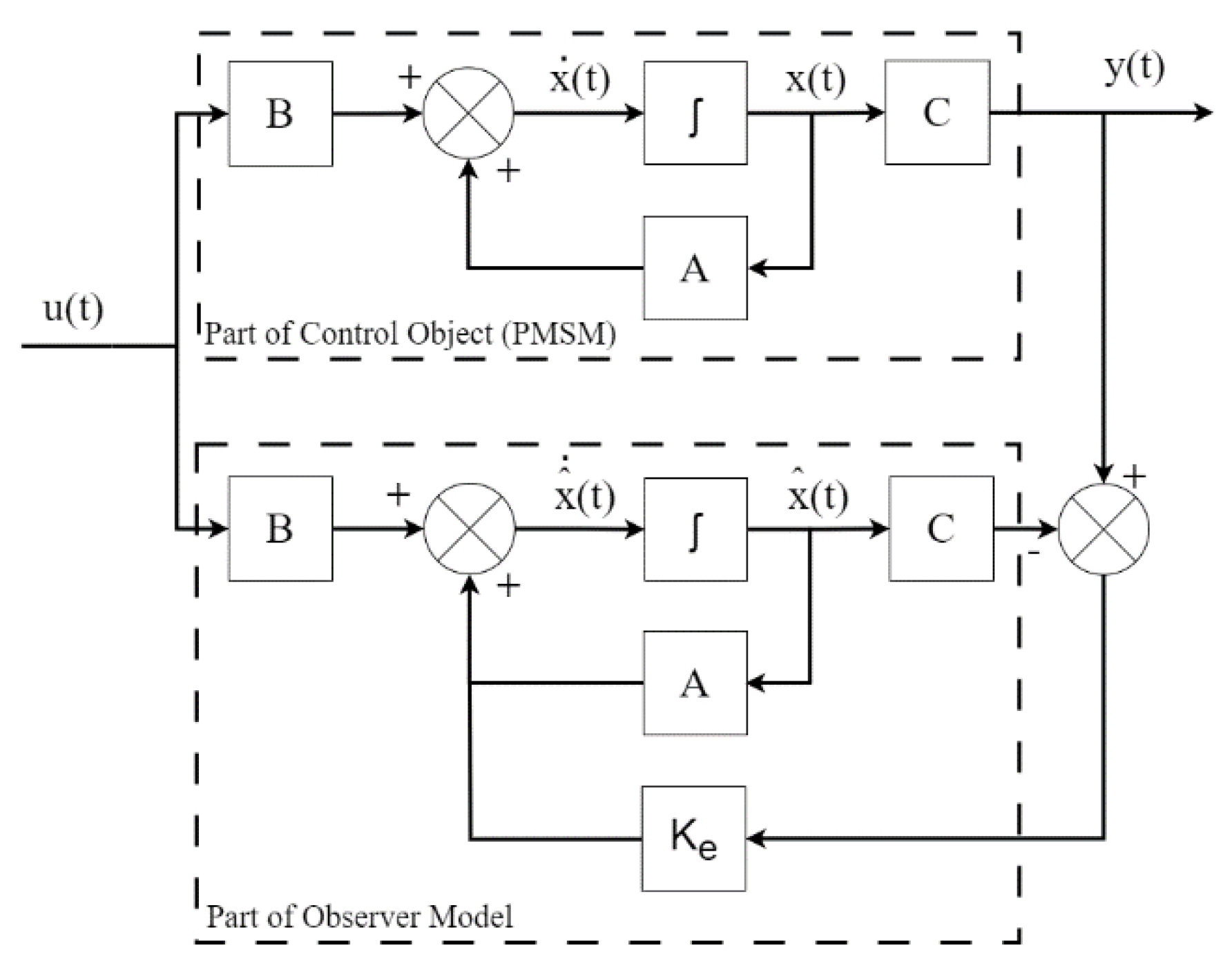
Figure 5.
The schematic diagram of proposed motor control device.
Figure 6.
The laboratory prototype of proposed motor control device.
Figure 7.
The equivalent circuit and flow of ringing conditions in inverter including parasitic elements.
Figure 7.
The equivalent circuit and flow of ringing conditions in inverter including parasitic elements.
Figure 8.
The equivalent circuit and flow of ringing conditions in inverter including parasitic elements: (a) Typical configuration; (b) Configuration with capacitance in high and low side; (c) Configuration with ringing suppression circuit of proposed systems.
Figure 8.
The equivalent circuit and flow of ringing conditions in inverter including parasitic elements: (a) Typical configuration; (b) Configuration with capacitance in high and low side; (c) Configuration with ringing suppression circuit of proposed systems.
Figure 9.
The schematic of Gate Driver Circuit using IR2110PBF after amplification in isolated side: (a) Typical configuration; (b) Configuration with capacitance in high and low side; (c) Configuration with ringing suppression circuit of proposed systems.
Figure 9.
The schematic of Gate Driver Circuit using IR2110PBF after amplification in isolated side: (a) Typical configuration; (b) Configuration with capacitance in high and low side; (c) Configuration with ringing suppression circuit of proposed systems.
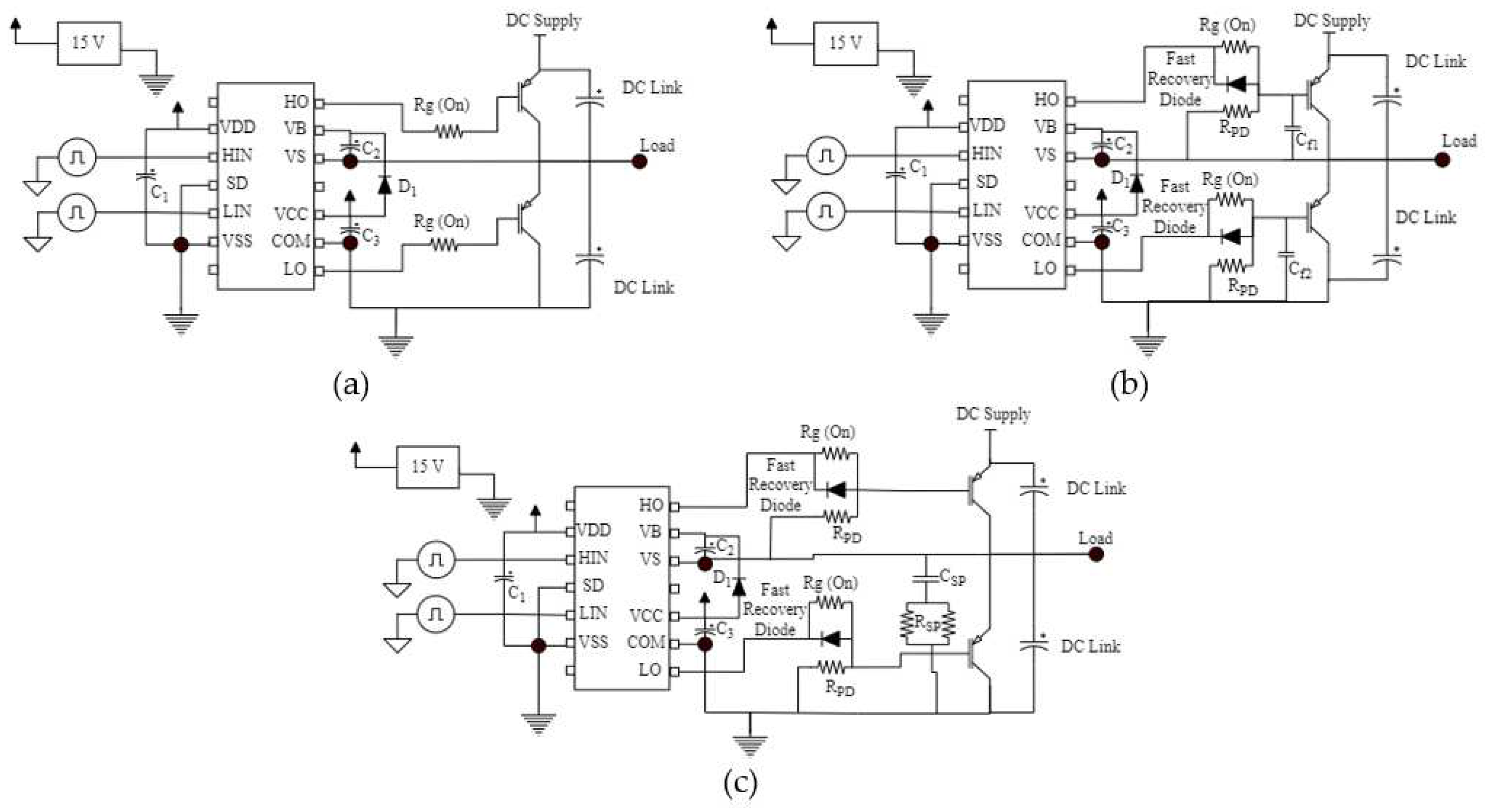
Figure 10.
The effect of ringing switching behavior in semiconductor material: (a) Reported behavior in previous research [26]; (b) Voltage spike in typical configuration; (c) Voltage spike of configuration using capacitance in high and low side; (d) Voltage spike of configuration using ringing suppression circuit of proposed systems.
Figure 11.
The experimental setup.
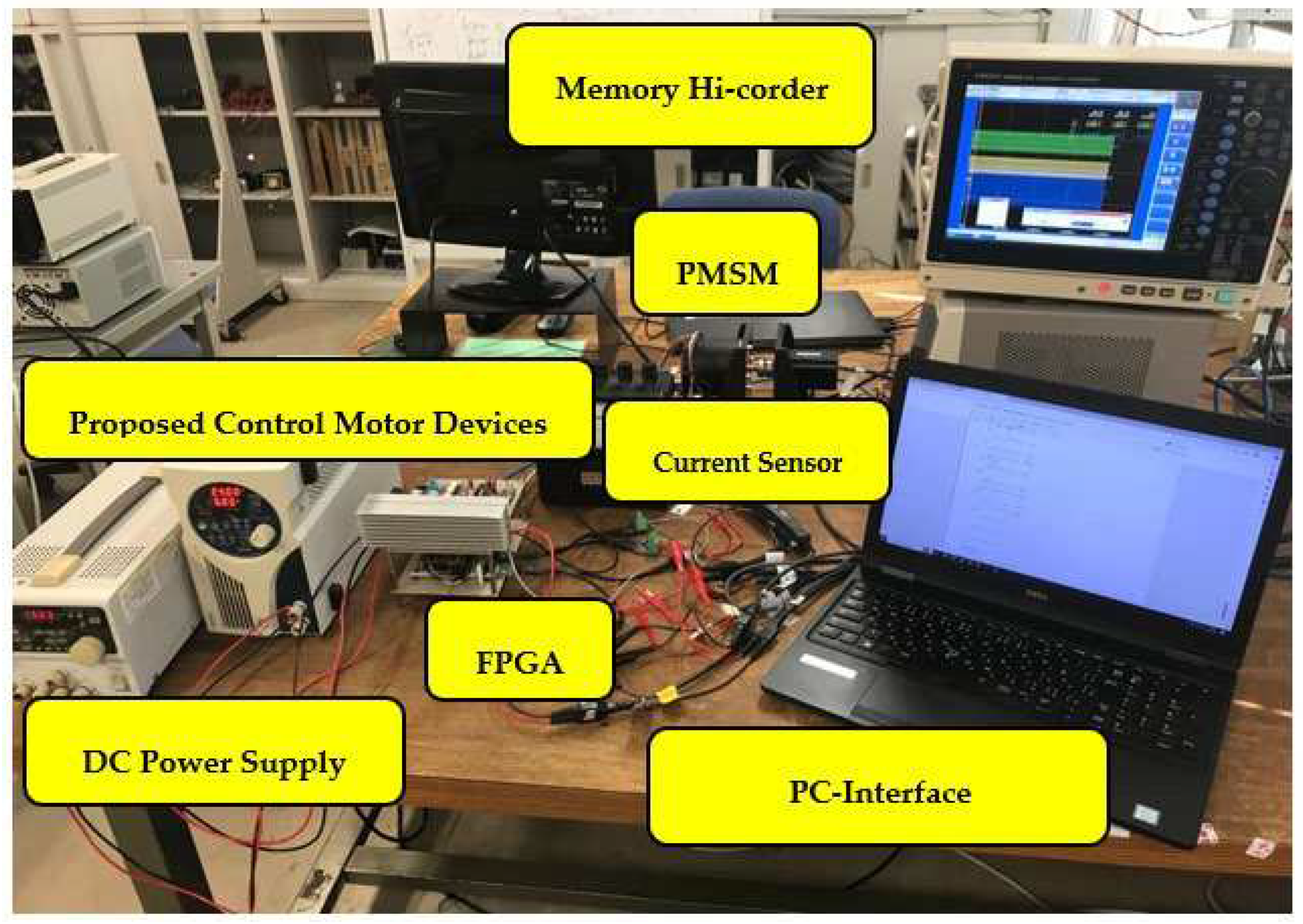
Figure 12.
The observation result of motor control devices using GDC by typical configuration IR2100PBF under peak current 3A: (a) Current measurement in Phase-A; (b) current measurement in Phase-B; (c) rotor position estimation by Back-EMF observer.
Figure 12.
The observation result of motor control devices using GDC by typical configuration IR2100PBF under peak current 3A: (a) Current measurement in Phase-A; (b) current measurement in Phase-B; (c) rotor position estimation by Back-EMF observer.
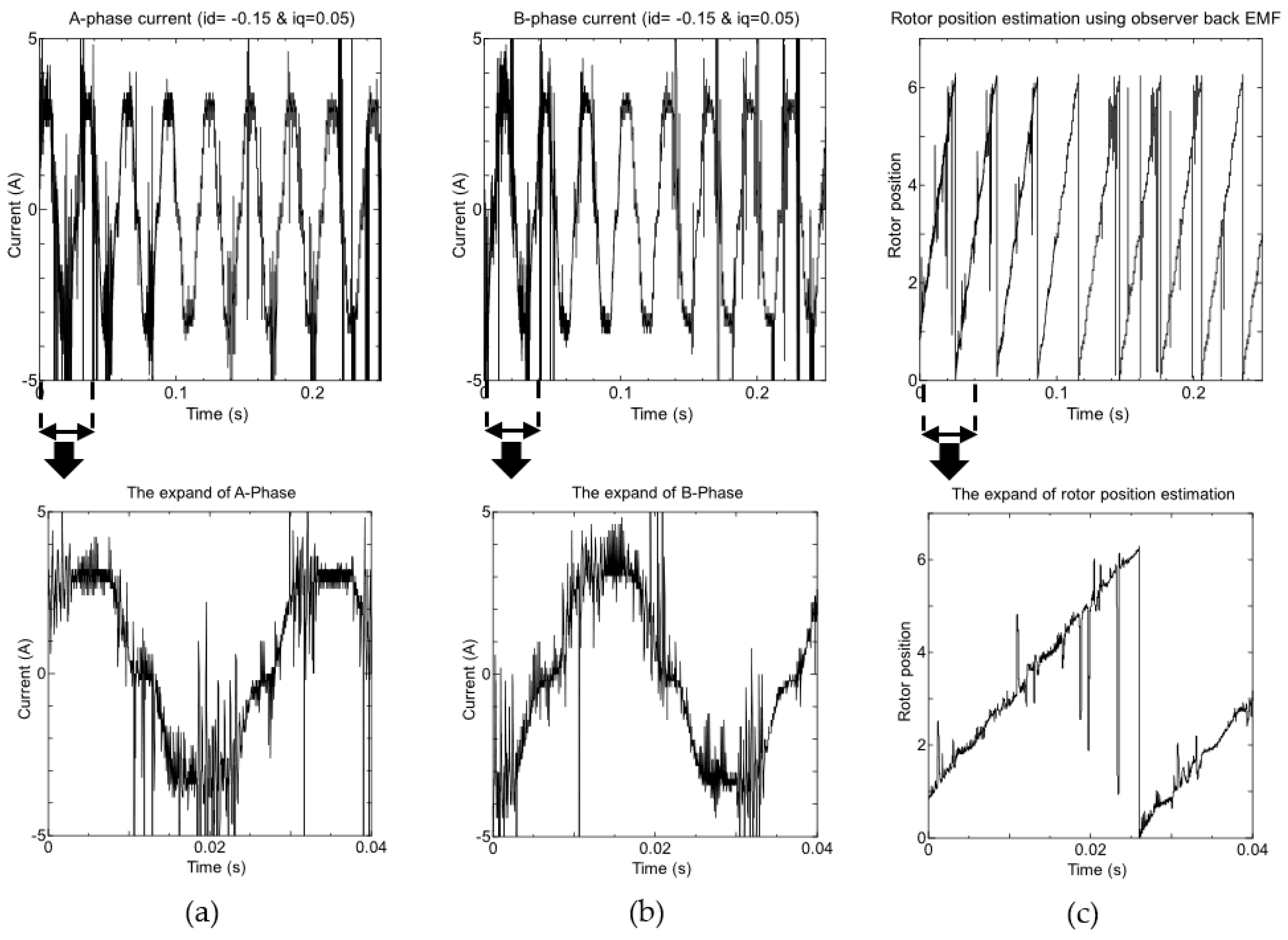
Figure 13.
The observation result of motor control devices using GDC by typical configuration IR2100PBF modified with capacitance in high and low side under peak current 3A: (a) Current measurement in Phase-A; (b) current measurement in Phase-B; (c) rotor position estimation by Back-EMF observer.
Figure 13.
The observation result of motor control devices using GDC by typical configuration IR2100PBF modified with capacitance in high and low side under peak current 3A: (a) Current measurement in Phase-A; (b) current measurement in Phase-B; (c) rotor position estimation by Back-EMF observer.
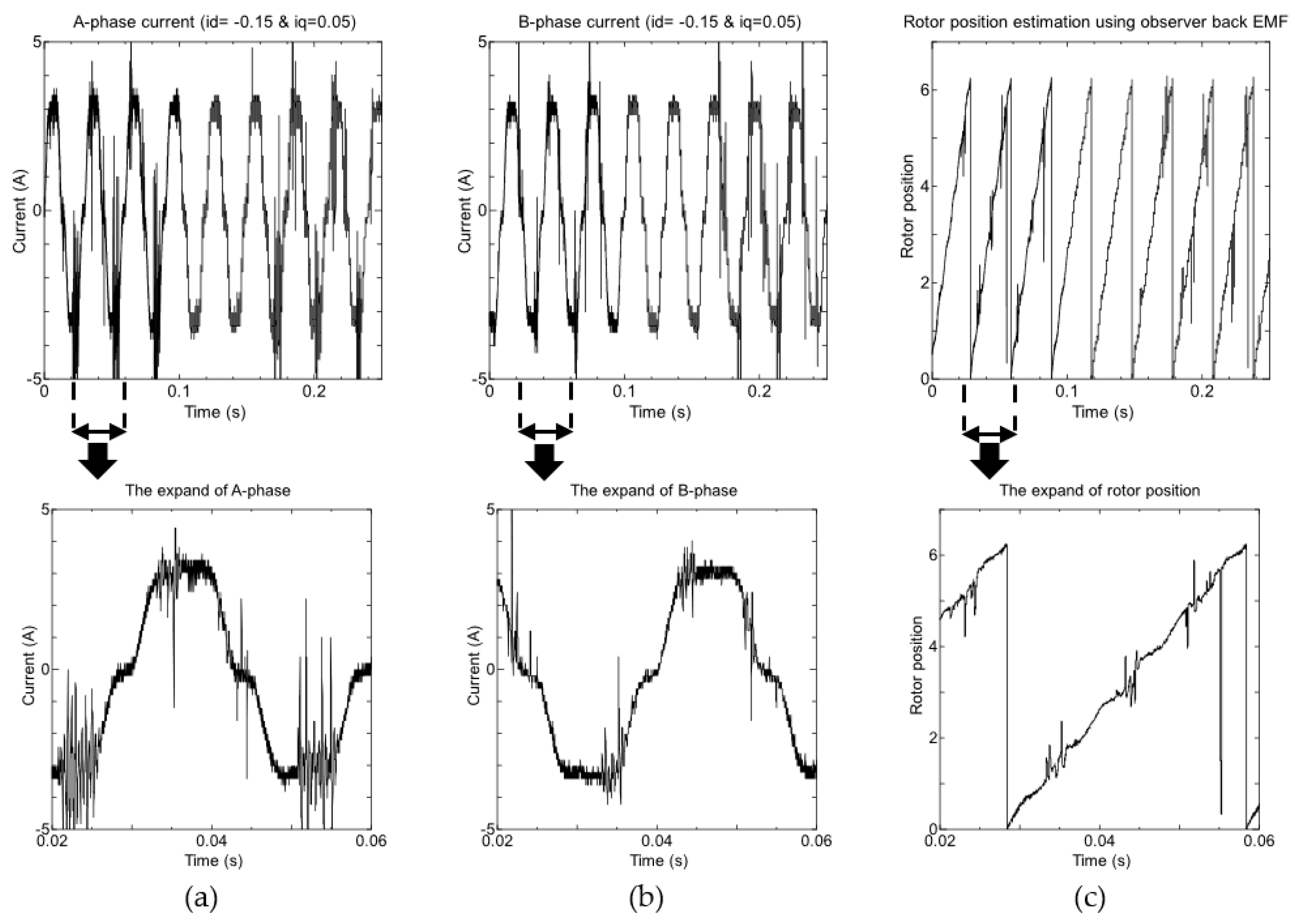
Figure 14.
The observation result of motor control devices using GDC by typical configuration IR2100PBF modified with ringing suppression circuit under peak current 3A: (a) Current measurement in Phase-A; (b) current measurement in Phase-B; (c) rotor position estimation by Back-EMF observer.
Figure 14.
The observation result of motor control devices using GDC by typical configuration IR2100PBF modified with ringing suppression circuit under peak current 3A: (a) Current measurement in Phase-A; (b) current measurement in Phase-B; (c) rotor position estimation by Back-EMF observer.
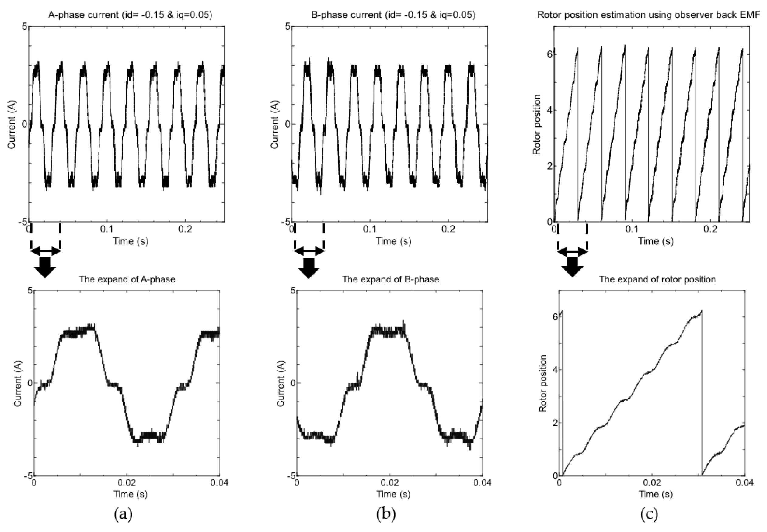
Figure 15.
The observation result of motor control devices using GDC by typical configuration IR2100PBF modified with ringing suppression circuit under peak current 4A: (a) Current measurement in Phase-A; (b) current measurement in Phase-B; (c) rotor position estimation by Back-EMF observer.
Figure 15.
The observation result of motor control devices using GDC by typical configuration IR2100PBF modified with ringing suppression circuit under peak current 4A: (a) Current measurement in Phase-A; (b) current measurement in Phase-B; (c) rotor position estimation by Back-EMF observer.
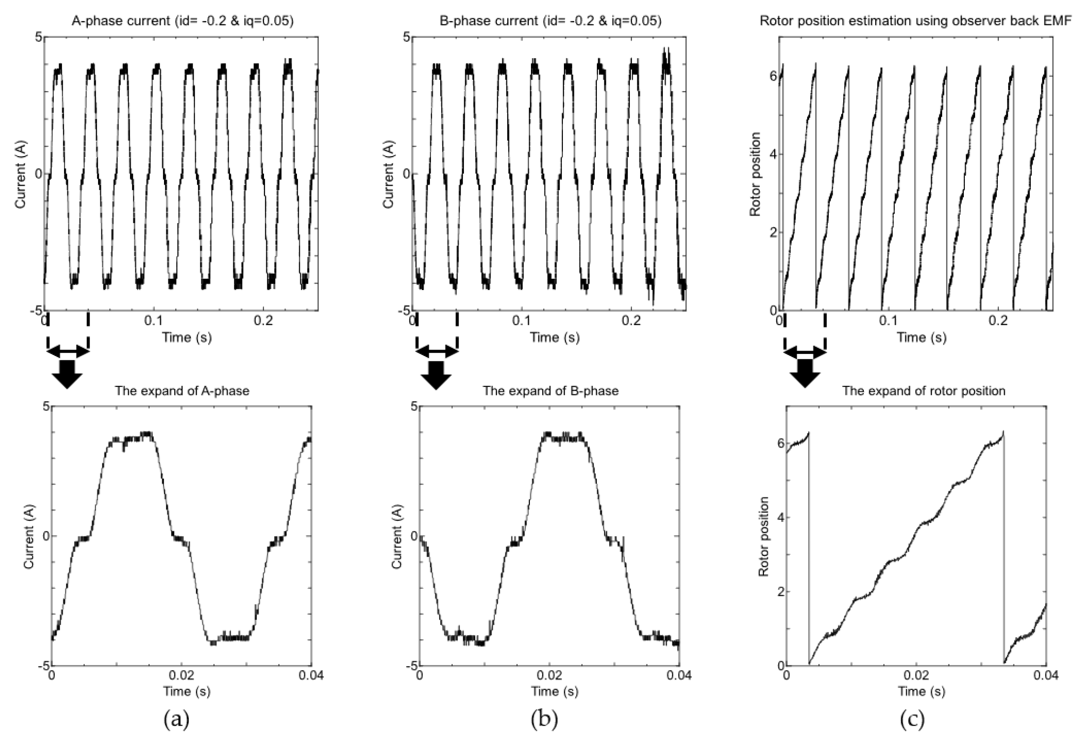

Table 1.
Comparison features by IC gate driver database.
| Parameter | Symbol | UCC27710 | TLP250H(F) | TC4424EPA | IR2110PBF (Proposed) |
|---|---|---|---|---|---|
| Manufacturer | - | Texas Instrument | Toshiba | Microchip | Infineon |
| Package/case/type | - | SOIC (8) | DIP (8) | PDIP (8) | PDIP (16) |
| Supply voltage | VCC | 10V | 10V | 4.5V | 10V |
| Operation of current supply | IQCC | 0.42mA | 5mA | 2.5mA | 0.34mA |
| Peak of current output / short circuit | IO | 1A | 2.5A | 3A | 2A |
| Turn-ON propagation delay | TON | 190ns | 500ns | 75ns | 150ns |
| Turn-ON rise time | Tr | 12ns | 50ns | 35ns | 25ns |
| Turn-OFF fall time | Tf | 11ns | 50ns | 35ns | 35ns |
| Latch-up protection | - | 1A | 1.5A | 1.5A | - |
| Required of additional isolation side | - | Yes | No | Yes | No |
| Required of signal conditioning | - | No | Yes | Yes | No |
| Reference | - | [22] | [23] | [24] | [25] |
Table 2.
Specification of equipment in experimental setup.
| Components | Specifications |
|---|---|
| DC Power Supply | (PSF-800L), (PW 18-1.3AT) |
| PMSM | DTBL-3518X (4 pole, 185W, 15A) |
| Current Sensor | PmodISNS20 (ACS722-20A) |
| ADC | ADCS7476 (12bit with rate conversion 1MSPS) |
| FPGA | ARTY Z7 pynq-20 |
| Memory HiCORDER | Hioki 8860-50 |
| PC Interface | Intel(R) Core (TM) i5-7200U |
Table 3.
The comparison of experimental result.
| Type of configuration | Max. Current spike | Max. Oscillation time | Impact of rotor position estimation |
|---|---|---|---|
| Typical (Test1) | 33% | 4ms | Large distortion appeared |
| Adding filter C (Test2) | <30% | 2ms | Large distortion appeared |
| Proposed (Test3) | <10% | <1ms | Large distortion not appeared |
Disclaimer/Publisher’s Note: The statements, opinions and data contained in all publications are solely those of the individual author(s) and contributor(s) and not of MDPI and/or the editor(s). MDPI and/or the editor(s) disclaim responsibility for any injury to people or property resulting from any ideas, methods, instructions or products referred to in the content. |
© 2023 by the authors. Licensee MDPI, Basel, Switzerland. This article is an open access article distributed under the terms and conditions of the Creative Commons Attribution (CC BY) license (http://creativecommons.org/licenses/by/4.0/).
Copyright: This open access article is published under a Creative Commons CC BY 4.0 license, which permit the free download, distribution, and reuse, provided that the author and preprint are cited in any reuse.


