Submitted:
27 October 2023
Posted:
30 October 2023
You are already at the latest version
Abstract
NUSES is a pathfinder satellite project hosting two detectors: Terzina dedicated to the study of ultra-high-energy cosmic rays (UHECRs) above 100 PeV and Zirè focused on the study of protons and electrons below 250 MeV and MeV gamma rays. This work concerns mainly the description of the Cherenkov camera, composed of SiPMs, for the Terzina telescope. Cherenkov light produced by extensive air showers induced by Ultra High Energy Cosmic Rays in the atmosphere could be detected from space, thus ensuring huge exposures. The Terzina telescope is being designed to detect such light. It has an effective area of about 0.1 m2 and an equivalent focal length of about 930 mm with a diameter of the circle containing 80% of the photons of less than 1 mm2. The photo-detection plane is composed of 2×5 SiPM arrays with 8×8 channels of 3×3 mm2 pixels each. To increase the data-taking period NUSES orbit will be sun-synchronous (with a height of about 550 km), thus allowing Terzina to point always towards the dark side of the Earth’s limb. The sun-synchronous orbit requires small distances to the poles, and as a consequence the expected dose received by the SiPMs will be 10 Gy during three year of NUSES mission. About 70% of the integral dose is delivered by the electrons and secondary gammas created in the mechanical structure and about 30% from protons. This estimation is done with the Geant4 simulation of the preliminary telescope geometry, without taking into account solar wind protons. We study the SiPM photo sensors under the irradiation received by the 50 MeV protons up to 30 Gy of total integrated dose corresponding to 9 years of the satellite operation.
Keywords:
SiPM
; UHECR
; Cherenkov telescope
1. Introduction
The NUSES (Neutrinos and Seismic Electromagnetic Signals) space mission aims to explore new technological and scientific pathways for future astroparticle physics [1,2]. The NUSES international collaboration, led by the Gran Sasso Science Institute, includes Istituto Nazionale di Fisica Nucleare (INFN), the Italian Space Agency, the University of Geneva in Switzerland, and the University of Chicago in the USA and the industrial partner Thales Alenia Space Italy (TAS-I) that will provide the satellite platform. The NUSES satellite will have a ballistic trajectory without orbital control. At the beginning of life (BoL) it will operate at an altitude of 535 km. The high inclination of 97.8 deg (LTAN = 18:00) orbit will allow a Sun-synchronous location of the satellite along the day-night boundary. The NUSES satellite will host two scientific apparatus namely Zirè [4,5] and Terzina [2,6] and will operate for three years.
Zirè will consist of a scintillating fiber tracker, a stack of plastic scintillator counters, an array of LYSO crystals, an active VETO system, and a Low Energy Module (LEM). It will perform spectral measurements of electrons, protons, and light nuclei below a few to hundreds of MeV. Zirè will also test innovative detection techniques for 0.1-10 MeV photons and monitor the Van Allen radiation belts.
Terzina will be a telescope specifically designed for the Cherenkov light detection, emitted by extensive-air showers (EAS) induced by ultra-high-energy cosmic rays (UHECRs) and neutrinos in the Earth’s atmosphere. This telescope will detect for the first time Cherenkov light created by EAS from space. We expect to detect protons-induced air showers with energies above 100 PeV, this will be a strong push forward for space-based instruments like POEMMA [7,8].
2. PMT vs SiPM
Terzina will be composed of an optical head unit (near-UV-optical telescope), a focal plane assembly (FPA) including the photo-sensitive SiPM camera and the readout integrated circuits, a thermal control system, and an external harness and electronic units, which will be in a separate box to shield from irradiation.
Some future space-based telescopes within Astor-particle physics, choose PMTs as the main component of the focal plane equipment. Table 1 shows a comparison between PMT and SiPM with selected parameters. One can notice that SiPMs are light and low power consumption devices with a good time and space resolution with respect to PMT. However, we need to emphasize that SiPMs are radiation and temperature-sensitive devices. Additionally, to detect light signals on the level of the single photon, a pre-amplifier needs to be a part of the readout chain.

Table 1.
Photo detector comparative table.
| Parameter | SiPM | PMT |
|---|---|---|
| Operation voltage | <100 V | ∼ 1000 V |
| Currents | ∼1 A | ∼100 A |
| Power per cm2 | ∼1 mW | ∼100 mW |
| Weight per cm2 of sensitive area | ∼10 g | ∼100 g |
| Total integrated charge | ∞ | ∼200 C |
| Single p.e. time resolution | <100 ps | ∼1 ns |
| Special resolution | ∼mm | ∼10 mm2 |
| Photo detection efficiency @ 400 nm | >50% | <50% |
| Temperature sensitive | yes | no |
| Need of pre-amplifier | yes | optional |
| Radiation resistance | low | high |
2 MA-PMT can have smaller channels 5×5 mm2 for example.
The Terzina photosensitive (detection) plane is composed of FBK [9] 2×5 SiPM arrays with 8×8 channels of 3×3 mm2 pixels. The sizes are approximate, with slight adjustments foreseen by the manufacturing company. We chose NUV-HD-MT [19] (Near Ultraviolet High Density with Metal Trench) SiPM family for our application.
Comparison between single p.e. responses for PMT and SiPM shown in Figure 1. The PMT shape is defined by the stochastic variation on the secondary electron emission from the first 2-3 dynodes. Simulation of a PMT, which describes the signal shape, can be found here [16]. The SiPM response shape, in more detail, is discussed in Section 3.
3. Parametric Simulation of the SiPM Response
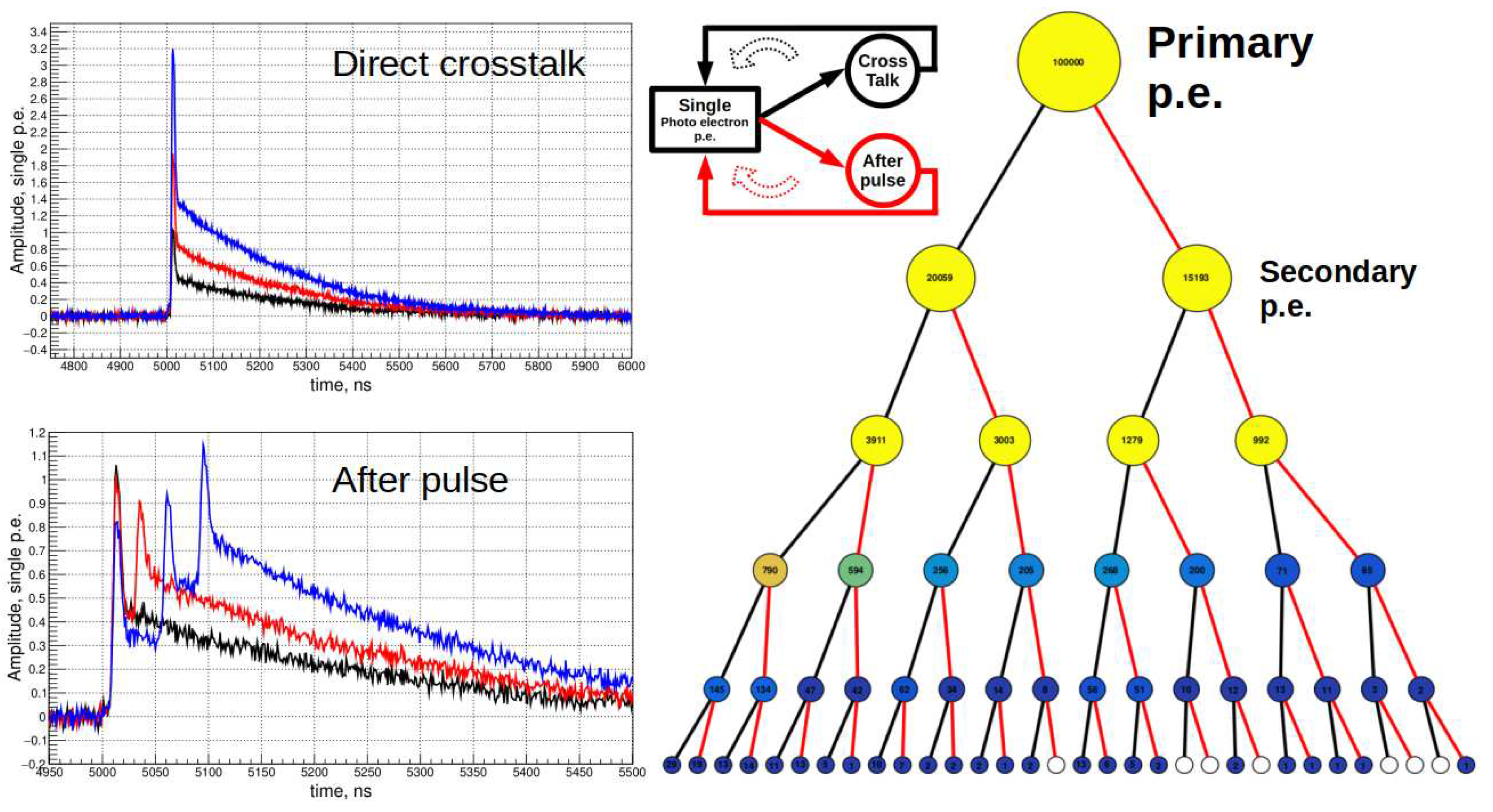
In this section, we briefly discuss the SiPM response simulation while an exhaustive description of the SiPM physics can be found here [10]. Our parametric simulation [17] takes as input waveform template of the first single p.e. response, amplitude vs. over-voltage, probability of the direct optical cross-talk (OCT), and after-pulse (AP) as a function of the SiPM over-voltage, after-pulse decay time, RMSE of the SiPM gain variation and RMSE of the electronic noise. The simulation is realized as a recursion of the physics processes: every time we generate the primary p.e. there is a probability to generate secondary p.e. via OCT or AP see Figure 2. The after-pulse process simulation takes into account a -cell recovery time. The process history avalanche tree of a single p.e. generation is shown in the right panel of Figure 2. One can notice that AP and OCT probability drops with the history depth for the AP branches. This is explained by the AP and OCT probability adjustment which is a function of its mother avalanche amplitude: when a -cell is not fully recharged it cannot generate a full avalanche and so the probability of AP/OCT is dropping. We assume a linear dependency between AP/OCT probability and amplitude of the avalanche1.
This simulation is a part of the full simulation chain of the Terzina telescope. It is used to estimate the trigger rates for the expected night glow background (NGB) and SiPM dark count rate (DCR) as a function of the electronic threshold. With this simulation we studied the effect of the different signal shapes on the rate see Figure 4 (right panel). We confirm our expectation: in the case of AC/DC coupling readout, by reducing the so-called slow component of the SiPM signal, one can significantly reduce the fake rate while keeping the same sensitivity to the signal.
Figure 2.
Left top panel: Example of the waveforms which includes only the OCT processes (the AP probability is set to 0). Left bottom panel: Example of the waveform which includes only AP processes (the OCT probability is set to 0). Right panel: The process history avalanche tree, the black line corresponds to OCT while the red line to AP.
4. SiPM Signal Waveform Characterisation
On Figure 3 (left panel) one can see the bias and readout schematics of SiPM. In the case of single photo operation, we are not able to see a signal with conventional oscilloscopes without an amplifier. We use short-duration light pulses from a 370 nm laser to flash all the -cells at the same time. As a result, we obtain ∼1 V signal with a shape roughly equal to a single -cells response. A SiPM operates at reverse bias voltage, however it can be powered with positive and negative voltages providing positive or negative output signals accordingly.
A SiPM signal tail can be fitted with an exponent as shown in Figure 3 (left panel) and its duration can be quantified as an exponent decay time (). This time is a function of the -cell capacitance hence its size.
We performed a set of measurements with three different configurations: by using LED (450 nm) and integration sphere, with a laser (370 nm) and an integration sphere, and with simply a laser. Figure 4 (left panel) summarises the obtained results. As expected the shortest decay time we measure with the last setup, where the integration sphere, which induced additional time spread, has been removed.
Figure 4.
Left: Measurements with a LED and Laser, with/without integration sphere, of the SiPM signal decay time as a function of a -cell size. Right: Rate at the fixed threshold as a function of a SiPM signal decay time.
Figure 4.
Left: Measurements with a LED and Laser, with/without integration sphere, of the SiPM signal decay time as a function of a -cell size. Right: Rate at the fixed threshold as a function of a SiPM signal decay time.
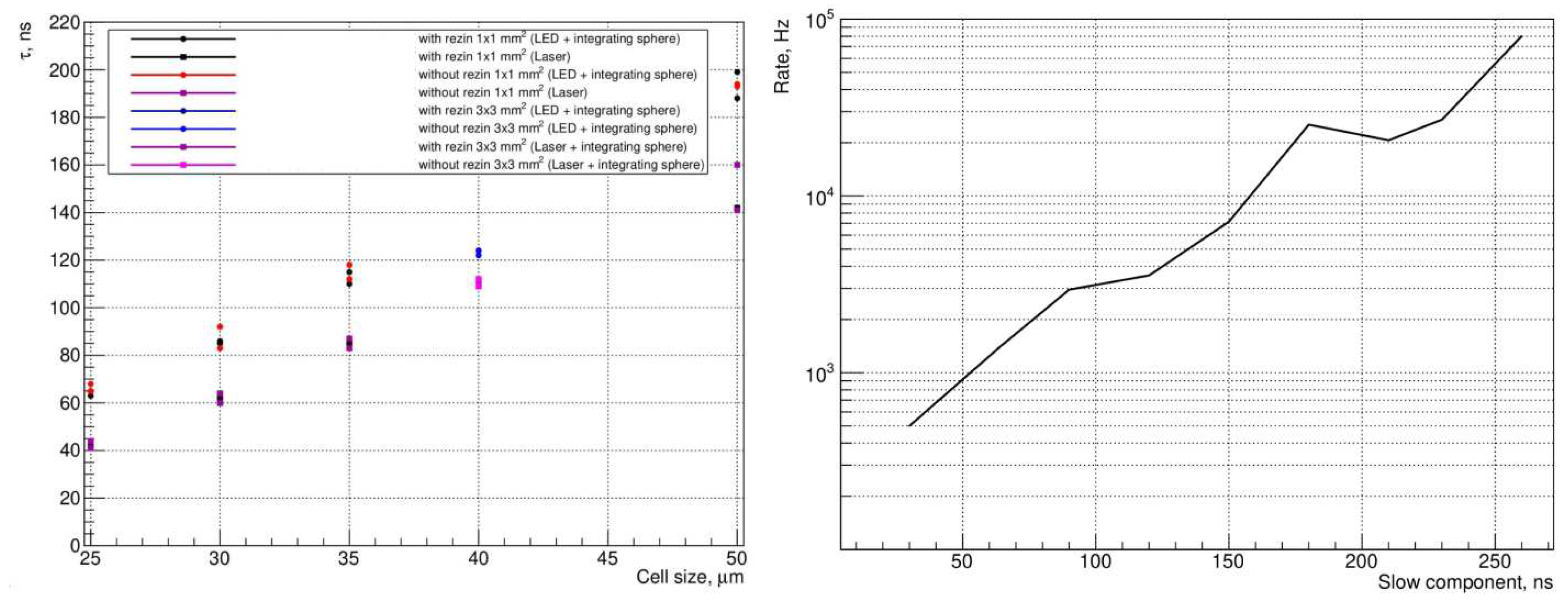
If we want to minimize only plus duration we have to choose SiPM with smaller -cell size. However, SiPMs with smaller -cell’s have smaller PDE due to a smaller fill factor. The final choice of the SiPM parameters will be based on full simulation where signal efficiency and background rate will be optimized.
5. Dose Estimation for Terzina Telescope
The trapped electrons and protons in the Van Hallen belts are responsible for the main radiation damage to the SiPMs and electronics. In this work, we do not consider the solar wind protons that can have a large impact on the total received dose.
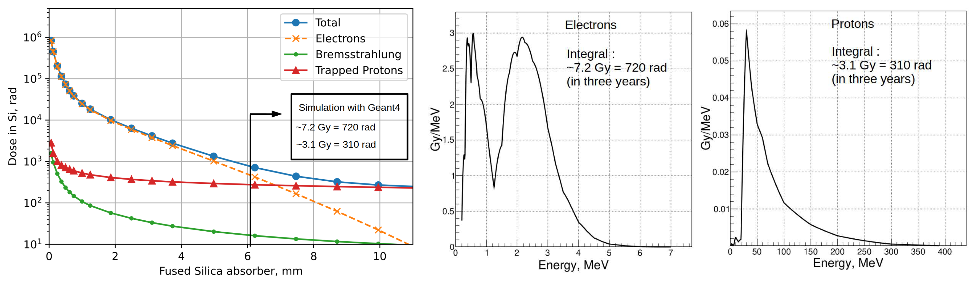
We use SPENVIS [11] machinery in two different ways to simulate the expected background signal on the camera. First, SPENVIS itself can estimate an accumulated dose assuming the oversimplified geometry. We choose geometry with two spheres one internal and one external. The external one is an absorber or can be considered as a shielding made of fused silica, the internal one, made of silicon, is a sensitive volume where we measure the dose. The dose in silicon with a variable layer of fused silica is shown in Figure 6. For unprotected surfaces on orbit, the radiation level is as high as rad Gy in 3 yr of exposure.
Moreover, SPENVIS provides us fluxes of the background particles for an orbit [18]. We injected the obtained SPENVIS electron and proton fluxes with an isotropic angular distribution as an input in our Geant4 [12,13] simulation of the telescope. In Figure 5 one can see the initial geometry of the Terzina telescope we consider. It consists of ∼12 mm of corrector lens made of fused silica (none crystalline quartz), primary and secondary mirrors made of aluminum with ∼2 mm thick wall, 2 mm of aluminum of the satellite walls. Figure 6 (right panel) shows the results of the simulation and its contribution as a function of particle energy. The estimated dose for three years of operation is 7.2 Gy for electrons and 3.1 Gy for protons. This estimation is done for the aluminum volume placed in the vicinity of the SiPM camera. With the same simulation, we estimate the Cherenkov background photon rate generated in the corrector lens: 181 Hz/mm produced by electrons and 0.16 Hz/mm produced by protons.
Doses obtained with Geant4-based simulation are in agreement with SPENVIS for ∼6 mm of fused silica protection.
Figure 5.
Left panel: Initial geometry of the Terzina telescope. Center: Example of the background electrons with ∼7 MeV energy producing Cherenkov light in the corrector lens and inducing dE/dx losses in the SiPM camera. Right panel: Zoom on the SiPM camera showing the aluminum volume where exactly we count the dose deposition.
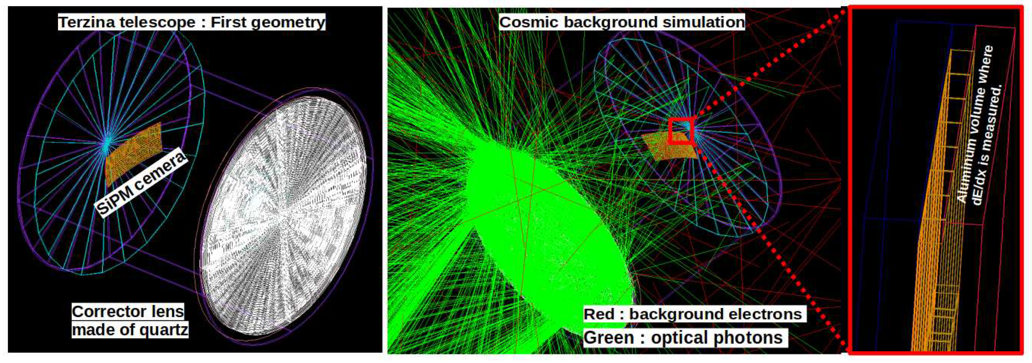
Figure 6.
Left panel: Dose in silicon obtained with SPENVIS for 3 years on Terzina’s orbit vs. thickness of fused silica shielding. Center, Right panel: Accumulated dose in the aluminum volume located in the vicinity of the camera and its readout electronics as a function of particle energy (for electrons and protons respectively). The total accumulated dose in 3 years in the aluminum plane is 7.2 Gy for electrons and 3.1 Gy for protons.
6. Irradiation of the SiPM with Protons
We performed a first proton irradiation test at IFJ PAN in Krakow [14] with a 50 MeV proton beam (Figure 7). The proton beam spot had a round shape with 35 mm diameter and planarity better than 5%. We tested SiPMs with different -cell sizes (25, 30, 35, 40, 50 m) and channel sizes (1 × 1 mm2 and 3 × 3 mm2) with/without entrance window.
After every new step of irradiation, we measured the IV curves to monitor an increase of a DCR (Figure 7). In the reverse bias mode, the absolute voltage range was between: [30, 50] V. In total, we performed 8 irradiation sessions. After each session the total received doses by the test samples are 1, 2, 3, 5, 7, 10, 20, 30 Gy. We observe an increase of the DCR with accumulated dose. Examples of a single p.e. signals before and after irradiation are shown in Figure 7 (right panel).
7. Background Created in a Window of a Photo Sensor
Background particles may create a Cherenkov light in any transparent medium (lens or surface of the mirror) in the telescope. Even if a source of optical photons background is located relatively far from light sensors still it can create additional undesired noise in the system. However, the background photons will be spread around sensitive area making it more easy to separate from the signal.
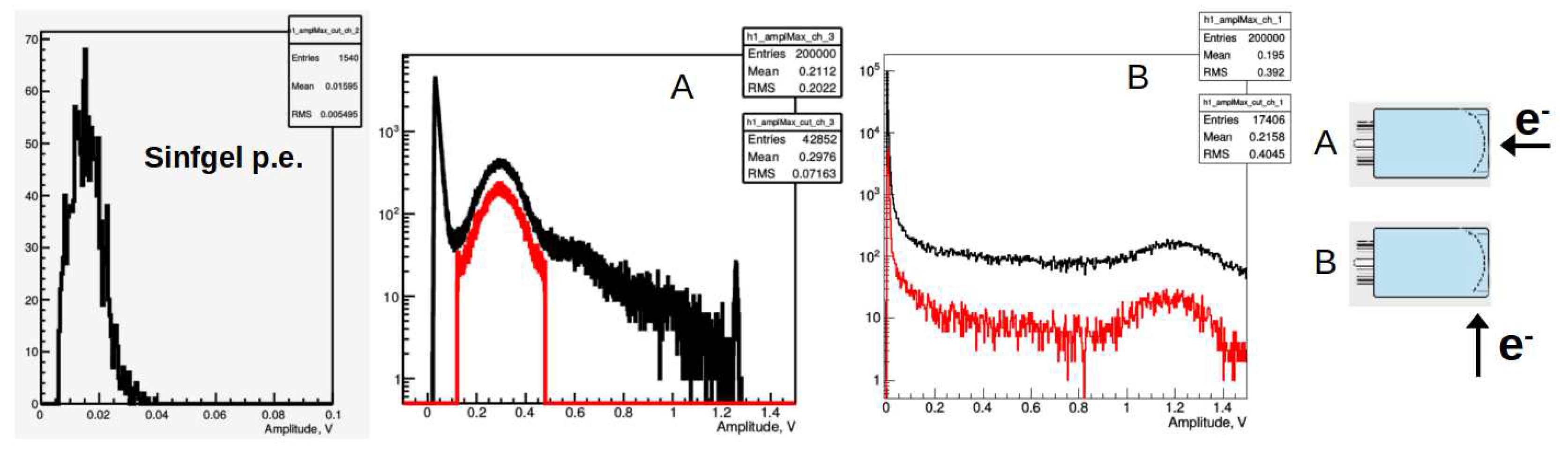
Usually, photo sensors contain a transparent window which is a radiator of Cherenkov light. Unavoidably PMTs are suffering from this source of background. We carried out the test with 5.6 GeV electrons provided by the DESY [15] accelerator facility. The experimental setup contained a PMT and plastic scintillator triggers installed after the PMT. We perform two tests: first (configuration A) - PMT was directly exposed to a perpendicular electron beam composed of individual electrons at 2 kHz rate and second (configuration B) - PMT was rotated by 90 degrees to the beam (see Figure 8).
Taking into account single p.e. amplitude (∼15 mV) we measured 19 p.e. and 75 p.e. created by Cherenkov light for two configurations respectively. The average window thickness of the PMT and its diameter is 3 mm and 25 mm which gives us 6 p.e./mm and 3 p.e/mm for two configurations. The second configuration has two times fewer photons because half of the Cherenkov photons from the cone are escaping the window.
This kind of background is suppressed in the case of SiPM sensors since one can have a very thin window or even be completely removed.
8. Conclusions
The usage of SiPM sensors in space applications will grow in the future. They are light, with low power consumption, high PDE, and good time and space resolution. However they are radiation and temperature sensitive, therefore a telescope design has to consider possible shields and thermostats.
Acknowledgments
NUSES is a joint project of the Gran Sasso Science Institute and Thales Alenia Space Italia, funded by the Italian Government (CIPE n. 20/2019 ), by the Italian Minister of Economic Development and the Abruzzo Region (MISE n. F/130087/00/X38), by the Italian Space Agency (ASI n. 15/2022) and by the Swiss National Foundation (SNF grant n. 178918). This project has received funding from the European Union’s Horizon Europe Research and Innovation programme under Grant Agreement No 101057511 (EURO-LABS).
Abbreviations
The following abbreviations are used in this manuscript:
| SiPM | Ailicon Photo-Multiplier |
| PMT | Photo-Multiplier tube |
| MA-PMT | Multy Anode Photo-Multiplier tube |
| NUSES | Neutrinos and Seismic Electromagnetic Signals |
| UHECR | Ultra High Energy Cosmic Rays |
| BoL | Beginning of Life |
| EoL | End of Life |
| LTAN | Local Time of Ascending Node |
| EAS | Extensive Air Showers |
| CR | Cosmic Rays |
| FPA | focal plane assembly |
| p.e. | photo electron |
| RMSE | Root mean square error |
| OCT | Optical Cross-Talk |
| AP | after-pulse |
| DCR | Dark count rate |
| FWHM | Full Width Half Maximum |
| PDE | Photon Detection Efficiency |
| NGB | Night Glow Background |
| NUV-HD-MT | Near Ultraviolet High Density Metal Trench SiPM. |
| 1 | The initial probability of the AP/OCT is given for fully recovered -cell. |
References
- I. De Mitri for the NUSES Collaboration, J. Phys.: Conf. Ser. 2429 (2023) 012007. [CrossRef]
- R. Aloisio for the NUSES Collaboration, POS 444 (2023) 391. 2023. [CrossRef]
- A. Di Giovanni and M. di Santo for the NUSES Collaboration, POS 414 (2022) 354, URL: https://pos.sissa.it/414/354.
- M. N. Mazziotta and R. Pillera, POS 444 (2023) 083. [CrossRef]
- M. F. Alonso, POS 444 (2023) 139. [CrossRef]
- L. Burmistrov for the NUSES Collaboration. arXiv:2304.11992. [CrossRef]
- A. V. Olinto et al. [The POEMMA Collaboration], “The POEMMA (Probe of Extreme Multi-Messenger Astrophysics) observatory,” JCAP 06 (2021), 007. arXiv:2012.07945.
- J. Krizmanic, et al. "POEMMA: Probe of extreme multi-messenger astrophysics." EPJ Web of Conferences. Vol. 210. EDP Sciences, 2019. [CrossRef]
- https://sd.fbk.eu/en.
- A. Gola et al. "NUV-Sensitive Silicon Photomultiplier Technologies Developed at Fondazione Bruno Kessler", Sensor 19 (2019) 308. [CrossRef]
- https://www.spenvis.oma.be/.
- S. Agostinelli et al., "GEANT4: A simulation toolkit", Nucl. Instrum. Meth. A506 (2003) 250–303. [CrossRef]
- http://geant4.web.cern.ch/geant4.
- J. Swakon et al. "Facility for proton radiotherapy of eye cancer at IFJ PAN in Krakow". [CrossRef]
- R. Diener et al. "The DESY II Test Beam Facility". [CrossRef]
- https://github.com/burmist-git/plume_PMT_sim_USBconv.
- https://gitlab.com/nuses-satellite-full-simulation/terzina_wfsim.
- https://github.com/burmist-git/spenvis.
- S. Merzi et al. "NUV-HD SiPMs with metal-filled trenches". [CrossRef]
Figure 1.
Left panel: Single p.e. response of a SiPM, the first peak are events when only one p.e. is detected, others, when the primary p.e. triggers other micro-cells, either via optical cross-talk or after-pulses or/and other physical phenomenon accruing in a SiPM. Right panel: Single p.e. response of a PMT. The simulation is shown in red for a single p.e. and blue for two p.e., while the black line corresponds to the measurements done with a pulsed LED (450 nm) signal. The majority of the tigers (LED pulses) contain no photons. Numbers of p.e. arriving at the anode, after an amplification dynodes stages, is shown on the x-axis.
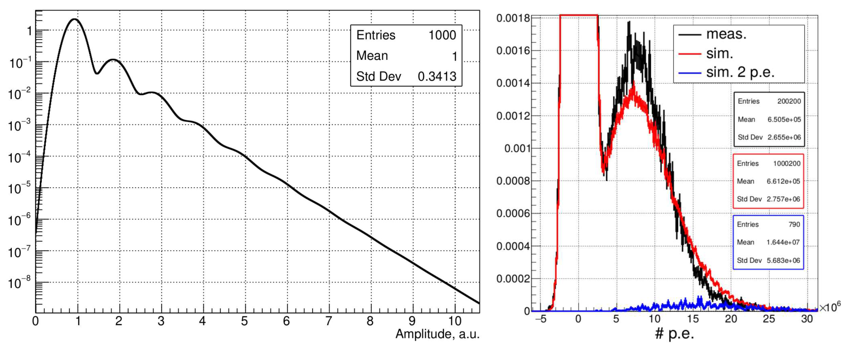
Figure 3.
Left: SiPM response to 370 nm laser with ∼25 ps pulse duration (FWHM) in saturation mode (all -cell produce an avalanche). The waveform was recorded with a 2 GHz oscilloscope. Right: Fit with an exponent of the SiPM signal tail. We measure 44 ns decay time for 25-m cell size.
Figure 3.
Left: SiPM response to 370 nm laser with ∼25 ps pulse duration (FWHM) in saturation mode (all -cell produce an avalanche). The waveform was recorded with a 2 GHz oscilloscope. Right: Fit with an exponent of the SiPM signal tail. We measure 44 ns decay time for 25-m cell size.

Figure 7.
Left panel: Photo of the SiPM samples installed in IFJ PAN proton beam facility. The light spot indicates the proton beam location. Center: The measured SiPM current as a function of bias voltage for different accumulated doses ( mm2, 25-m cell). Right panel: Waveform of SiPM signal recorded in dark conditions and corresponding to a single p.e. signals before (red) and after irradiation (black).
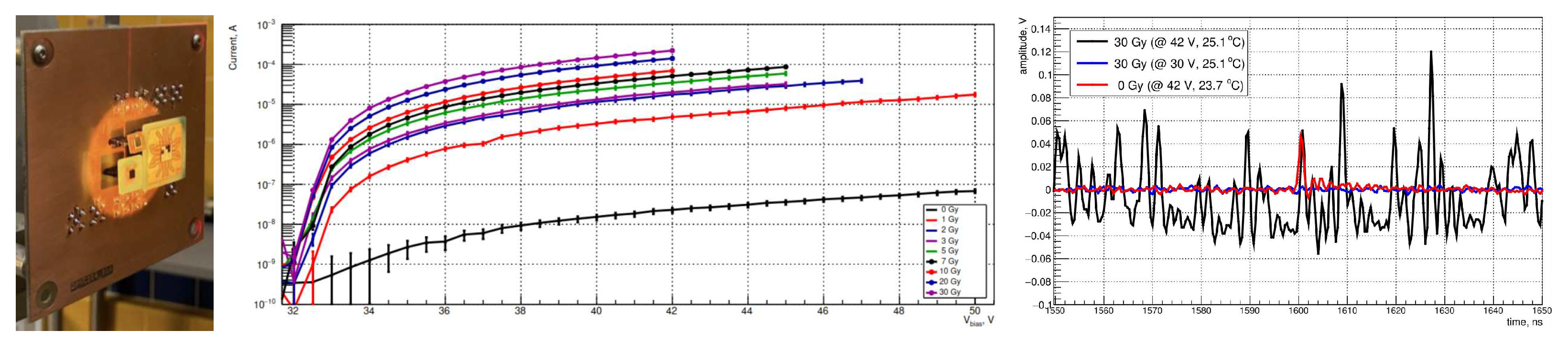
Figure 8.
Left panel: Single p.e. amplitude distribution of the PMT measured with laser. Center: Amplitude of the signal from the 5.6 GeV electron impinged perpendicularly to the PMT surface. The black curve corresponds to all the measured events while the red one requires a coincidence with a plastic scintillator restricting only nonscattered events. Right panel: Amplitude of the signal from the 5.6 GeV electron impinged parallel to the PMT surface.
Disclaimer/Publisher’s Note: The statements, opinions and data contained in all publications are solely those of the individual author(s) and contributor(s) and not of MDPI and/or the editor(s). MDPI and/or the editor(s) disclaim responsibility for any injury to people or property resulting from any ideas, methods, instructions or products referred to in the content. |
© 2023 by the authors. Licensee MDPI, Basel, Switzerland. This article is an open access article distributed under the terms and conditions of the Creative Commons Attribution (CC BY) license (http://creativecommons.org/licenses/by/4.0/).
Copyright: This open access article is published under a Creative Commons CC BY 4.0 license, which permit the free download, distribution, and reuse, provided that the author and preprint are cited in any reuse.


