Submitted:
16 October 2023
Posted:
16 October 2023
You are already at the latest version
Abstract
In this paper, we study the effect of parasitic channel on electrical characteristics and power consumptions of vertically stacked gate-all-around (GAA) silicon nanosheet (NS) MOSFETs of the bulk and silicon-on-insulator (SOI) substrates. Through deliberate control of the bottom parasitic channel coverage, we systematically assess its influence on DC, AC, and RF characteristics including power consumption. The observed findings highlight a significant differentiation among the bottom parasitic channels: GAA (i.e., control sample with 100% coverage), omega-shaped gate NS (70% and 80% coverages), and FinFET (60% coverage). Compared with the device with a 60% coverage channel, the device with a 100% coverage channel possesses 3520% and 8030% normalized leakage current improvement for both NFET and PFET under the bulk substrate, respectively. Compared with bulk-substrate devices, the SOI-substrate devices further significantly improve the leakage current. Due to enhanced off-state current leakages in the 100% covered bulk-substrate device, the static power demonstrates a notable improvement (about 98.1%), compared to 60% covered devices. Hence, the utilization of a 60% covered channel will result in a degradation of both device and circuit performance. The observation of GAA NS MOSFET indicates that an increase in the bottom parasitic channel coverage ratio leads to a positive impact on power consumption and leakage currents. The examination presented here is useful in the fabrication of stacked GAA NS MOSFETs.
Keywords:
gate-all-around
; nanosheet
; silicon-on-insulator
; vertically stacked
; parasitic channel
; short-channel effect
; current densities
; gate capacitances
; transconductance
; cut-off frequency
; 3dB frequency
; power consumption
; 3-D device simulation
1. Introduction
A key component of the advancement of integrated circuit design technology has been the miniaturization of transistors [1,2,3]. In recent years, transistor scaling has been exemplified by Moore’s Law, which has significantly increased the performance of devices [4,5]. However, in addition to the compelling advantages of cost reduction and performance enhancement, the continuous scaling of transistors has raised challenging issues concerning short-channel effects (SCE) and device reliability concerns [6,7,8]. Consequently, further transistor scaling has been hindered [9]. Conventional planar MOSFETs have evolved into multigate FETs to address these SCE challenges, including double-gate and three-dimensional (3-D) fin-field effect transistors [10,11] as well as gate-all-around (GAA) MOSFETs [12,13]. Notable examples of GAA structures are nanowire (NW) and nanosheet (NS) configurations [14,15]. Because of their robust control over SCEs, bulk, and Silicon-On-Insulator (SOI) FinFETs emerged as promising substitutes for planar MOSFETs during the transition to sub-22-nm technology around 2012 [16]. In spite of this, FinFETs encountered performance limitations as semiconductor technology advanced to nodes smaller than 5-nm [17,18,19]. They became susceptible to SCEs and reliability issues, compounded by fabrication challenges associated with further scaling. GAA NS MOSFETs have since emerged as compelling candidates for sub-5-nm nodes [17,20], offering both superior performance standards and desired capabilities [21,22].
In GAA NS MOSFETs, the gate surrounds the channel from all directions, thereby bolstering the gate’s electrostatic integrity over the channel [23]. This design innovation not only enables a reduction in supply voltages but also sustains gate drive capabilities, paving the way for high-performance applications in advanced technology nodes [24,25]. During the fabrication of GAA NS MOSFETs on Si bulk substrates, Si nanosheets are released through the wet etching of SiGe sacrificial layers [26,27,28]. Additionally, the high-k-metal-gate (HKMG) is deposited on the bulk, SOI substrates, and this results in the formation of the bottom parasitic channel [29]. Unlike the upper channels of stacked GAA NS MOSFETs, which are wrapped surrounded gates, the bottom parasitic channel is solely controlled by only the top gate (Fin shape) [30]. Consequently, this channel can function as a leakage path during the off-sate, impacting the overall performance of the GAA NS MOSFETs and circuit [22,31]. To address this concern, recent efforts have focused on various approaches related to suppressing the parasitic leakage in GAA devices, with a particular emphasis on the bottom dielectric isolation (BDI) [27], punchthrough stopper (PTS), buried oxide beneath the gate area [32]. This is because the substrate of GAA NS MOSFETs serves as the planer channel region. These techniques have been investigated to decrease off-state leakage current by blocking the source-to-drain leakage path [18,31]. Furthermore, Y. Choai et al. have reported that increasing the height of the bottom parasitic channel further decreases leakage current [31]. In a typical PTS structure, p-type substrates are used for NFETs and n-type substrates for PFETs and they are moderately doped to prevent punchthrough between the source, drain, and substrate. However, only the top vertically stacked channels of an NFET are utilized, and an aggressively high PTS doping process is employed to minimize the current flow through the NFET bottom channel [33,34]. Consequently, the PTS structure is susceptible to band-to-band tunneling current from drain to substrate junction. This phenomenon is associated with a negative or zero gate bias, causing a strongly doped p+/n+ junction to function as a reverse-biased tunneling p+/n+ diode. Moreover, in the case of SOI substrates, the insulator layer beneath the source/drain regions increases the thermal resistance to the heat sink path, which exacerbates the self-heating effect [33]. Despite these considerations, there has been a lack of systematic studies on the influence of parasitic channels and their coverage ratios in the GAA NS MOSFETs with bulk- and SOI-substrate devices on circuit performance and power consumption.
In this research, we investigate the impact of different bottom parasitic channel coverage ratios on the output and transfer characteristics, transient behavior, and power consumption of GAA Si NS MOSFETs with bulk and SOI substrates. We systematically examine how different coverage ratios of bottom parasitic channels: specifically, 60%, 70%, 80%, and control sample (i.e., 100%), affect the DC, AC, and RF characteristics of the devices. To comprehensively analyze the influence of the bottom parasitic channel coverage ratios on the characteristics of GAA devices, we employ intensive 3-D device simulations. Our primary findings reveal a substantial reduction in leakage current as the bottom parasitic channel coverage ratio increases, holding true for both bulk and SOI substrates.
The rest of this paper is structured as follows. Section II provides a concise presentation of the simulated device structure, highlighting variations in the bottom parasitic channel coverage ratio. In Section III, we delve into an in-depth examination of the outcomes, encompassing DC, AC, and RF characteristics, as well as power consumption, all of which are influenced by the presence of bottom parasitic leakage channels and control samples. Finally, in Section IV, we draw our study to a conclusion.
2. 3-D Device Simulation
In Figure 1a, we present a transmission electron microscope (TEM) image of fabricated GAA NS MOSFETs [26]. Figure 1b shows the simulated 3-D device which is constructed based on Figure 1c of the fabricated device. The design of a 16-nm gate length GAA Si NS device with dimensions of 25-nm width and 5-nm height is accomplished through the 3-D device simulation. To prevent leakage current from the source to the drain in the substrate, the substrate is doped with high concentrations (1019 cm-3) of boron (NFETs) or arsenic (PFETs). Figure 1d–g illustrate 2-D cross-sectional views (cut along the cut line-C1 of Figure 1b) along the channel under the different coverage ratios of bottom parasitic leakage channels, specifically for the bulk-substrate devices. It’s worth noting that similar considerations for bottom parasitic channel coverages are applied to GAA Si NS MOSFETs with SOI substrates. The adopted physical dimensions, doping concentrations of the channel, source, drain, and source/drain extensions, as well as the utilized metal work function, effective oxide thickness, achieved characteristics, and SCEs of the 60%-covered channel device, are listed in Table 1. To ensure the physical accuracy of our vertically stacked GAA Si NS MOSFETs, we conducted calibration of our device simulation against measurement data [26], a process we have previously detailed in our prior work [12]. In this simulation, we utilized a calibrated mobility model, in particular, we intensively employed 3-D quantum mechanically corrected device simulations to evaluate device characteristics [35]. For validation purposes, we examined the conduction band energy and electron density along the channel during on and off states by numerically solving the 3-D density gradient equation along with drift-diffusion (DG+DD) and nonequilibrium Green’s functions (NEGF) models [36,37,38,39]. Not shown here, but by adjusting the electron effective mass, the simulation results of the DG+DD model are in good agreement with those of the NEGF model [40]. In our device simulation, we have properly incorporated doping dependence, high-field saturation, and impurity scattering mobility models into our device simulation [41,42].
3. Results and Discussion
- i).
- Impact of Parasitic Channel on Transfer and Output Characteristics
To gain deeper insights into the impact of different bottom parasitic channel coverage ratios on GAA Si NS MOSFET, we conducted 3-D TCAD simulations using Sentaurus TCAD tools [43]. Additionally, we conducted a comparative analysis of leakage currents among the bulk- and SOI-substrate devices. Figure 2a,b depict the simulated ID-VG curves for both NFET and PFET, considering the different bottom parasitic channel coverage ratios under the linear and saturation drain bias conditions. Analysis of these ID-VG curves reveals a pronouncedly higher leakage current for the 60% coverage bottom parasitic channel compared to the other coverage ratios. Overall, when GAA Si NS MOSFETs operate under linear drain bias conditions with different bottom parasitic channel coverage ratios, they exhibit enhanced gate control and reduced drain-induced barrier lowering (DIBL) effect. These factors collectively contribute to a lower leakage current, as depicted in Figure 2a. In contrast, saturation drain bias exhibits a more substantial variation in leakage current with different coverage of the bottom parasitic channel, as shown in Figure 2b. Furthermore, our study extends to calculating the normalized leakage current, expressed as ((I leakage_60% - I leakage_control sample) / Ileakage_60%) × 100%). Figure 2c,d illustrate the off-state leakage current of NFETs and PFETs with different coverage ratios of parasitic channels under linear and saturation drain bias conditions. Remarkably, in; linear and saturation drain bias conditions, as opposed to the 60% coverage channel, the normalized leakage for both NFET and PFET demonstrates substantial enhancements of 194%, 453% (linear drain bias), and 3520%, 8030% (saturation drain bias), respectively, in the case of the 100% coverage channel. It is noteworthy that as the bottom channel functions similarly to a planar MOSFET, the increased coverage ratio of the bottom parasitic channel further improves the leakage current, primarily attributed to enhanced channel confinement and reduced floating body effect. Figure 3a–d portray simulated 2-D cross-sectional of off-state current densities of the investigated devices with different coverage ratios of bottom parasitic channels. These results clearly indicate that the 60% coverage of the bottom parasitic channel exhibits a significantly higher current density in the bulk- and SOI-substrate devices, establishing it as the primary source of substantial leakage in the device. Furthermore, it is observable that as the coverage ratio increases (from 60% to 100%) for the bottom parasitic channel, the current density correspondingly decreases. Notably, the mitigation of parasitic channel leakage is significantly achieved through 80% coverage, characterized by an omega shape bottom parasitic channel, facilitated by vertically stacked NS channel release via wet etching. However, achieving 100% channel coverage release for the bottom channel becomes unfeasible, making beyond 80% coverage a viable option. Similar to the bulk-substrate devices, the SOI-substrate devices are analyzed, with simulated ID-VG curves presented in Figure 4a,b. Results indicate that the SOI-substrate devices exhibit enhanced leakage currents attributed to the insulating BOX layer, which isolates the device from the substrate. This isolation effectively suppresses floating body effect and reduces junction leakage from source to drain. The normalized leakage for NFET and PFET in SOI substrates is found to be less than 165%, as demonstrated in Figure 4c,d. Furthermore, Figure 5a–d depict off-state current densities of SOI-substrate devices under different coverage ratios of bottom parasitic channels. Due to strong isolation from the substrate, the current distribution is almost uniform across all coverage ratios. Consequently, the leakage current of SOI-substrate devices with different coverage ratios of bottom parasitic channels exhibits significant improvement.
In Figure 6a,b, we present a comparative analysis of ID-VD characteristics among bulk- and SOI-substrate devices, considering different coverage ratios of bottom parasitic channels under different gate voltages. Notably, the ID of the 60% coverage ratio of the channel is consistently lower than that of the other coverage ratios across each gate bias condition. Moreover, we conducted calculations to determine the normalized improvement in ID for NFETs and PFETs, revealing substantial enhancements of 8.5% under each gate bias condition in the case of the 100% covered channel. Furthermore, we extended our analysis to simulate the transconductance (gm), a fundamental parameter with significant implications in radio frequency (RF) design as it directly influences gain and cut-off frequency. Figure 7a,b illustrate the gm-VG relationship for different coverage ratios of bottom parasitic channels in bulk- and SOI-substrate devices. It’s noteworthy that gm exhibits an increasing trend with an escalation in the different coverage ratios of the bottom parasitic channels. Remarkably, in the case of 100% coverage, a notably larger value of gm is observed when compared to the other coverage ratios.
- ii).
- Impact of Parasitic Channel on AC, RF, and Transient Characteristics
A major AC characteristic to consider is parasitic capacitance, specifically the total gate capacitance (CG) determined directly from AC curves measured under strong inversion conditions. In Figure 8a,b, we present a comparative analysis of CG-VG characteristics among the bulk- and SOI-substrate devices, considering different coverage ratios of bottom parasitic channels while operating at a frequency of 1 GHz and a drain voltage of 0.05 volts. Our analysis clearly identifies that an increased coverage ratio of the bottom parasitic channel leads to a corresponding increase in CG. This phenomenon is attributed to the expansion of the bottom parasitic channel coverage ratio, which in turn increases the channel surface area in contact with the gate. This expanded surface area significantly contributes to the enlargement of the gate capacitance, as the gate capacitance is directly proportional to the area of overlap between the gate and the channel.
The inset in Figure 9a illustrates a common-source amplifier circuit designed for high-frequency (RF) applications. In this circuit, a sinusoidal input wave with an amplitude of 0.05 volts is applied, and the circuit operates within the range of VG = 0.4 V and VD = 0.5 V. The voltage gain curves in decibels (dB) versus the input signal frequency, considering bulk and SOI substrates under the different coverage ratios of the bottom parasitic channel, are presented in Figure 9a and Figure 9b, respectively. Remarkably, the samples with 100% coverage, whether on bulk or SOI substrates, exhibit notably higher voltage gain, cut-off frequency (fT), and 3-dB frequency (f3dB), as highlighted in Figure 9c,d. Notably, the 100% covered device (indicated by the red line) achieves a voltage gain of 18.6 dB. We calculate this voltage gain at a frequency of 107 Hz, and estimate fT using the unitary voltage gain, and determine f3dB using the 3-dB point voltage gain, as defined by
We observe a substantial variation in voltage gain as we transition from 60% to 100% coverage ratios of the bottom parasitic channel, particularly at low frequencies. As the signal frequency increases, we note a reduction in the extent of voltage gain variation among the different coverage ratios of the bottom parasitic channels. It’s important to highlight that a voltage gain of unity is achieved at the cut-off frequency, which defines fT as
In the given equation, gm represents the transconductance, and CG represents the gate capacitance. For the device featuring 100% coverage of the bottom parasitic channel with a bulk-substrate device, the voltage gain, f3dB, and fT are measured at 18.6 dB, 37.2 GHz, and 374 GHz, respectively. Similarly, for the SOI-substrate device with 100% coverage of the parasitic channel, the voltage gain, f3dB, and fT are recorded as 18.5 dB, 57.5 GHz, and 525.3 GHz, respectively. These fT values are influenced by the variations in gm and CG under the respective coverage ratio conditions of the bottom parasitic channels.
Figure 10a,b provide a comprehensive overview of the transient response observed in the GAA Si NS MOSFET inverter circuit and show input and output behaviors over time under varying coverage conditions of the bottom parasitic channels. The inverter transient analysis encompasses two primary conditions: i) NFET turned on while PFET is off, and ii) PFET turned on while NFET is off, as illustrated in the zoom-in plots presented in Figure 10c,d. From these plots, we extract important parameters such as falling time (tf), rising time (tr), high-to-low delay time (tHL), and low-to-high delay time (tLH) for the input and output signals, as depicted in Figure 10c,d. Notably, the scenario with a 60% coverage ratio of the bottom parasitic channel exhibits pronounced variations, primarily due to the presence of parasitic leakage in the bottom channel, leading to significant power fluctuations. It’s essential to highlight that tHL is directly proportional to CG and inversely proportional to the Ion of NFET, while tLH follows a similar relationship but is associated with PFET. Figure 10e provides a comprehensive listing of estimated timing values for different coverage ratios of the bottom parasitic channels, demonstrating a clear trend where increased bottom parasitic channel coverage leads to decreased timings. During the high-to-low signal transition of the output signal, the delay time is initially governed by the signal transition’s starting points and subsequently controlled by the on/off-state of NFET in the inverter. Consequently, the threshold voltage of NFET significantly influences tHL. Similarly, tLH is notably impacted by the threshold voltage of PFET. Analogous to the investigation into the transient response of CMOS inverter with bulk substrates, we extended our study to examine the transient characteristics of CMOS inverter with SOI substrate under the different coverage ratios of the bottom parasitic channels, as depicted in Figure 11. Our findings reveal that SOI-substrate devices, benefiting from substrate oxide isolation, exhibit reduced leakage. Interestingly, the timings of these SOI-substrate devices remain relatively unaffected by the varying coverage ratios of the bottom parasitic channels. Furthermore, we delve into the assessment of the total power (Ptotal), which encompasses dynamic power (Pdyn), short-circuit power (PSC), and static power (Pstat) for different coverage ratios of the bottom parasitic channels. These results shed valuable light on the substantial impact of bottom parasitic channels on GAA Si NS CMOS inverter performance, providing critical insights for device optimization and enhancing power efficiency.
The Ptotal is derived by summing the Pstat, PSC, and Pdyn. The definitions of these power components are as follows:
where the Ileakage is the leakage current that flowing between the power rails during at static operation, Ileakage is defined as follows,
Pstat will be consumed as long as the VDD is opened, regardless of the switching activity between the input and output.
where denotes the clock rate. While ISC refers to the shot-circuit current, ISC is achieved when both the NFET and PFET devices are concurrently activated, establishing a direct current path between the power rails. T represents the switching period.
Pdyn depends on the load capacitance, represented as, sum of the CG of both NFET and PFET at on-state condition,
Figure 12a,b present a detailed analysis of the estimated power consumption components, including Pstat, Pdyn, Psc, and Ptotal, under the different coverage ratios of the bottom parasitic channels for bulk- and SOI-substrate devices. The findings consistently reveal a reduction in all power consumption components as the coverage ratio of the parasitic channel increases. Of particular significance is the observation that Pstat, which exhibits notable normalized values of 98.1% and 50% for both bulk and SOI substrates, respectively, in the case of 100% coverage of the bottom parasitic channels. This outcome can be attributed to the strong dependence of Pstat on the leakage current, which is significantly influenced by the coverage ratio of the bottom parasitic channel.
4. Conclusions
In summary, our study extensively investigates the electrical characteristics, RF performance, transient behavior, and power consumption while varying the coverage of the bottom parasitic channel in GAA NS devices under the bulk and SOI substrates. We have found that the increase of the bottom channel coverage ratio results in an improvement of leakage current. Remarkably, the SOI-substrate devices have demonstrated a substantial reduction in leakage current, compared to bulk-substrate devices. Furthermore, our investigation has highlighted those devices featuring 80% and 100% coverage ratio of the bottom parasitic channel exhibiting noteworthy improvement in the off-state leakage and static power consumption. This suggests that, from a manufacturing perspective, achieving 80% coverage ratio of the bottom parasitic channel offers a practical approach to minimize parasitic channel leakage. However, it remains a challenge to establish a 100% coverage ratio of the bottom GAA channel, representing an open problem in current research.
Author Contributions
Conceptualization, S. R. Kola and Y. Li; methodology, S. R. Kola and Y. Li; software, S. R. Kola and Y. Li; validation, S. R. Kola and Y. Li; formal analysis, S. R. Kola and Y. Li; investigation, S. R. Kola and Y. Li; resources, Y. Li; data curation, S. R. Kola; writing—original draft preparation, S. R. Kola and Y. Li; writing—review and editing, S. R. Kola and Y. Li; visualization, S. R. Kola and Y. Li; supervision, Y. Li; project administration, Y. Li; funding acquisition, Y. Li. All authors have read and agreed to the published version of the manuscript.
Funding
This work was supported in part by the National Science and Technology Council (NSTC), Taiwan, under Grant NSTC 112-2221-E-A49-171, and Grant NSTC 112-2218-E-006-009-MBK; and in part by the ‘‘2022 Qualcomm Taiwan Research Program, National Yang Ming Chiao Tung University (NYCU),’’ under Grant NAT-487835 SOW.
Institutional Review Board Statement
Not applicable.
Informed Consent Statement
Not applicable.
Data Availability Statement
Not applicable.
Conflicts of Interest
The authors declare no conflict of interest.
References
- Huang, C.Y.; Dewey, G.; Mannebach, E.; Phan, A.; Morrow, P.; Rachmady, W.; Tung, I.C.; Thomas, N.; Alaan, U.; Paul, R.; et al. 3-D Self-Aligned Stacked NMOS-on-PMOS Nanoribbon Transistors for Continued Moore’s Law Scaling. in Tech. Dig. - Int. Electron Devices Meet. IEDM 2020, 425–428. [CrossRef]
- Moroz, V.; Lin, X.W.; Asenov, P.; Sherlekar, D.; Choi, M.; Sponton, L.; Melvin, L.S.; Lee, J.; Cheng, B.; Nannipieri, A.; et al. DTCO Launches Moore’s Law over the Feature Scaling Wall. in Tech. Dig. - Int. Electron Devices Meet. IEDM 2020, 913–916. [CrossRef]
- Chau, R. Process and Packaging Innovations for Moore’s Law Continuation and Beyond. in Tech. Dig. - Int. Electron Devices Meet. IEDM 2019, 1–6. [CrossRef]
- Han, G.; Hao, Y. Design Technology Co-Optimization towards Sub-3 Nm Technology Nodes. J. Semicond. 2021, 42, 2–4. [CrossRef]
- Mukesh, S.; Zhang, J. A Review of the Gate-All-Around Nanosheet FET Process Opportunities. Electron. 2022, 11. [CrossRef]
- Kola, S.R.; Li, Y.; Chuang, M.H.; Endo, K.; Samukawa, S. Statistical Analysis of Intrinsic High-Frequency Characteristic Fluctuation of Emerging Silicon Gate-All-Around Nanosheet (NS) MOSFETs at Sub-3-Nm Nodes. in 7th IEEE Electron Devices Technol. Manuf. Conf., EDTM 2023 2023, 1–3. [CrossRef]
- Kola, S.R.; Li, Y.; Chen, C.; Chuang, M. Statistical 3D Device Simulation of Full Fluctuations of Gate-All-Around Silicon Nanosheet MOSFETs at Sub-3-Nm Technology Nodes. in 2022 Int. Symp. VLSI Technol. Syst. Appl. VLSI-TSA 2022 2022, 2021–2022. [CrossRef]
- Kola, S.R.; Li, Y.; Chen, C.; Chuang, M. A Unified Statistical Analysis of Comprehensive Fluctuations of Gate-All-Around Silicon Nanosheet MOSFETs Induced by RDF , ITF , and WKF Simultaneously. in Int. Symp. Qual. Electron. Des. 2022, 1–6. [CrossRef]
- Mocuta, A.; Weckx, P.; Demuynck, S.; Radisic, D.; Oniki, Y.; Ryckaert, J. Enabling CMOS Scaling towards 3nm and Beyond. in Dig. Tech. Pap. - Symp. VLSI Technol. 2018, 147–148. [CrossRef]
- Kola, S.R.; Chuang, M.; Li, Y. Characteristics Fluctuation of Sub-3-Nm Bulk FinFET Devices Induced by Random Interface Traps. in 2023 IEEE 23rd Int. Conf. Nanotechnol. 2023, 917–922. [CrossRef]
- Kola, S.R.; Li, Y.; Thoti, N. Random Telegraph Noise in Gate-All-around Silicon Nanowire MOSFETs Induced by a Single Charge Trap or Random Interface Traps. J. Comput. Electron. 2020, 19, 253–262. [CrossRef]
- Sung, W.L.; Li, Y. Characteristics of Stacked Gate-All-Around Si Nanosheet MOSFETs with Metal Sidewall Source/Drain and Their Impacts on CMOS Circuit Properties. IEEE Trans. Electron Devices 2021, 68, 3124–3128. [CrossRef]
- Lee, S.; Jeong, J.; Yoon, J.S.; Lee, S.; Lee, J.; Lim, J.; Baek, R.H. Sensitivity of Inner Spacer Thickness Variations for Sub-3-Nm Node Silicon Nanosheet Field-Effect Transistors. Nanomaterials 2022. [CrossRef]
- Sreenivasulu, V.B.; Kumari, N.A.; Lokesh, V.; Ajayan, J.; Uma, M.; Vijayvargiya, V. Design of Resistive Load Inverter and Common Source Amplifier Circuits Using Symmetric and Asymmetric Nanowire FETs. J. Electron. Mater. 2023, 134, 1–13. [CrossRef]
- Kola, S.R.; Li, Y.; Thoti, N. Characteristics of Gate-All-Around Silicon Nanowire and Nanosheet MOSFETs with Various Spacers. in Int. Conf. Simul. Semicond. Process. Devices, SISPAD 2020, 79–82.
- Li, Y.; Hwang, C.H.; Han, M.H. Simulation of Characteristic Variation in 16 Nm Gate FinFET Devices Due to Intrinsic Parameter Fluctuations. Nanotechnology 2010, 21. [CrossRef]
- Vashishtha, V.; Clark, L.T. Comparing Bulk-Si FinFET and Gate-All-around FETs for the 5 Nm Technology Node. Microelectronics J. 2021, 107, 104942. [CrossRef]
- Seon, Y.; Chang, J.; Yoo, C.; Jeon, J. Device and Circuit Exploration of Multi-Nanosheet Transistor for Sub-3 Nm Technology Node. Electronics 2021, 10, 1–14. [CrossRef]
- Sun, C.J.; Wu, C.H.; Yao, Y.J.; Lin, S.W.; Yan, S.C.; Lin, Y.W.; Wu, Y.C. Threshold Voltage Adjustment by Varying Ge Content in SiGe P-Channel for Single Metal Shared Gate Complementary FET (CFET). Nanomaterials 2022, 12. [CrossRef]
- Yang, J.; Huang, Z.; Wang, D.; Liu, T.; Sun, X.; Qian, L.; Pan, Z.; Xu, S.; Wang, C.; Wu, C.; et al. A Novel Scheme for Full Bottom Dielectric Isolation in Stacked Si Nanosheet Gate-All-Around Transistors. Micromachines 2023, 14, 1107. [CrossRef]
- Li, Y.; Chou, H.; Lee, J. Nanowire FinFETs. IEEE Trans. Nanotechnol. 2005, 4, 510–516.
- Gu, J.; Zhang, Q.; Wu, Z.; Luo, Y.; Cao, L.; Cai, Y.; Yao, J.; Zhang, Z.; Xu, G.; Yin, H.; et al. Narrow Sub-Fin Technique for Suppressing Parasitic-Channel Effect in Stacked Nanosheet Transistors. IEEE J. Electron Devices Soc. 2022, 10, 35–39. [CrossRef]
- Li, Y.; Hwang, C.H. The Effect of the Geometry Aspect Ratio on the Silicon Ellipse-Shaped Surroundinggate Field-Effect Transistor and Circuit. Semicond. Sci. Technol. 2009, 24, 095018. [CrossRef]
- Sreenivasulu, V. B.; Nelam, A. K.; Kola, S.R.; Sing, J.; Li, Y. Exploring the Performance of 3-D Nanosheet FET in Inversion and Junctionless Modes : Device and Circuit-Level Analysis and Comparison. IEEE Access 2023, 11, 90421–90429. [CrossRef]
- Kola, S.R.; Li, Y.; Chuang, M. Intrinsic Parameter Fluctuation and Process Variation Effect of Vertically Stacked Silicon Nanosheet Complementary Field-Effect Transistors. in Int. Symp. Qual. Electron. Des. 2023, 1–8.
- Loubet, N.; Hook, T.; Montanini, P.; Yeung, C.; Kanakasabapathy, S.; Guillorn, M.; Yamashita, T.; Zhang, J.; Miao, X. Stacked Nanosheet Gate-All-Around Transistor to Enable Scaling Beyond FinFET T230 T231. in VLSI Technol. 2017 2017, 230–231.
- Zhang, J.; Pancharatnam, S.; Adams, C.; Wu, H.; Zhou, H.; Shen, T.; Xie, R.; Sankarapandian, M.; Wang, J.; Watanabe, K.; et al. Full Bottom Dielectric Isolation to Enable Stacked Nanosheet Transistor for Low Power and High Performance Applications. in Tech. Dig. - Int. Electron Devices Meet. IEDM 2019, 250–253. [CrossRef]
- Zhang, Q.; Gu, J.; Xu, R.; Cao, L.; Li, J.; Wu, Z.; Wang, G.; Yao, J.; Zhang, Z.; Xiang, J.; et al. Optimization of Structure and Electrical Characteristics for Four-layer Vertically-stacked Horizontal Gate-all-around Si Nanosheets Devices. Nanomaterials 2021, 11, 1–15. [CrossRef]
- Zhang, J.; Ando, T.; Yeung, C.W.; Wang, M.; Kwon, O.; Galatage, R.; Chao, R.; Loubet, N.; Moon, B.K.; Bao, R.; et al. High-k Metal Gate Fundamental Learning and Multi-VT Options for Stacked Nanosheet Gate-All-around Transistor. in Tech. Dig. - Int. Electron Devices Meet. IEDM 2018, 537–540. [CrossRef]
- Vardhan, P.H.; Ganguly, S.; Ganguly, U.; Gaa, A.N. Threshold Voltage Variability in Nanosheet GAA Transistors. IEEE Trans. Electron Devices 2019, 66, 4433–4438.
- Choi, Y.; Lee, K.; Yeon Kim, K.; Kim, S.; Lee, J.; Lee, R.; Kim, H.M.; Suh Song, Y.; Kim, S.; Lee, J.H.; et al. Simulation of the Effect of Parasitic Channel Height on Characteristics of Stacked Gate-All-around Nanosheet FET. Solid. State. Electron. 2020, 164, 107686. [CrossRef]
- Yoo, S.; Kim, S.Y. Leakage Optimization of the Buried Oxide Substrate of Nanosheet Field-Effect Transistors. IEEE Trans. Electron Devices 2022, 69, 4109–4114. [CrossRef]
- Jegadheesan, V.; Sivasankaran, K.; Konar, A. Optimized Substrate for Improved Performance of Stacked Nanosheet Field-Effect Transistor. IEEE Trans. Electron Devices 2020, 67, 4079–4084. [CrossRef]
- Mertens, H.; Ritzenthaler, R.; Hikavyy, A.; Kim, M.S.; Tao, Z.; Wostyn, K.; Chew, S.A.; De Keersgieter, A.; Mannaert, G.; Rosseel, E.; et al. Gate-All-Around MOSFETs Based on Vertically Stacked Horizontal Si Nanowires in a Replacement Metal Gate Process on Bulk Si Substrates. in Dig. Tech. Pap. - Symp. VLSI Technol. 2016, 1–2. [CrossRef]
- Dasgupta, A.; Parihar, S.S.; Member, G.S. BSIM Compact Model of Quantum Confinement in Advanced Nanosheet FETs. IEEE Trans. Electron Devices 2020, 67, 730–737.
- Seoane, N.; Martinez, A.; Brown, A.R.; Barker, J.R.; Asenov, A. Current Variability in Si Nanowire MOSFETs Due to Random Dopants in the Source/Drain Regions: A Fully 3-D NEGF Simulation Study. IEEE Trans. Electron Devices 2009, 56, 1388–1395. [CrossRef]
- Carrillo-Nunez, H.; Dimitrova, N.; Asenov, A.; Georgiev, V. Machine Learning Approach for Predicting the Effect of Statistical Variability in Si Junctionless Nanowire Transistors. IEEE Electron Device Lett. 2019, 40, 1366–1369. [CrossRef]
- Wang, W.; Covi, E.; Lin, Y.H.; Ambrosi, E.; Ielmini, D. Modeling of Switching Speed and Retention Time in Volatile Resistive Switching Memory by Ionic Drift and Diffusion. in Tech. Dig. - Int. Electron Devices Meet. IEDM 2019, 763–766. [CrossRef]
- Li, Y.; Cheng, H.W. Random Interface-Traps-Induced Electrical Characteristic Fluctuation in 16-Nm-Gate High-κ/Metal Gate Complementary Metal-Oxide-Semiconductor Device and Inverter Circuit. Jpn. J. Appl. Phys. 2012, 51, 04DC08. [CrossRef]
- Li, Y.; Chang, H.T.; Lai, C.N.; Chao, P.J.; Chen, C.Y. Process Variation Effect, Metal-Gate Work-Function Fluctuation and Random Dopant Fluctuation of 10-Nm Gate-All-around Silicon Nanowire MOSFET Devices. Tech. Dig. - Int. Electron Devices Meet. IEDM 2015, 887–890. [CrossRef]
- Ko, H.; Kang, M.; Jeon, J.; Shin, H. Modeling of Nanoplate Parasitic Extension Resistance and Its Associated Dependency on Spacer Materials. IEEE Trans. Electron Devices 2019, 66, 2527–2531. [CrossRef]
- Bhuwalka, K.K.; Wu, H.; Zhao, W.; Rzepa, G.; Baumgartner, O.; Benistant, F.; Chen, Y.; Liu, C. Optimization and Benchmarking FinFETs and GAA Nanosheet Architectures at 3-Nm Technology Node: Impact of Unique Boosters. IEEE Trans. Electron Devices 2022, 69, 4088–4094. [CrossRef]
- Sentaurus Device User Guide, Version O-2018.03, Synopsys, Mountain View, CA, USA, 2018.
Figure 1.
(a) Extraction of nanosheet width (WNS), nanosheet thickness (TNS), inter-channel separation (TSP) using the transmission electron microscope (TEM) image of vertically stacked GAA NS structure [26]. (b) A 3-D bird’s view of the simulated GAA Si NS MOSFET. (c) TEM image of one of the GAA NS MOSFET showing the variation in WNS, TNS, and TSP [26]. (d) 2-D view of 60% coverage ratio of bottom GAA channel (i.e., FinFET type channel). (e)-(f) 70% and 80% coverage ratios of bottom channel (i.e., omega shape GAA channels). (g) The control sample (100%) covered the bottom channel.
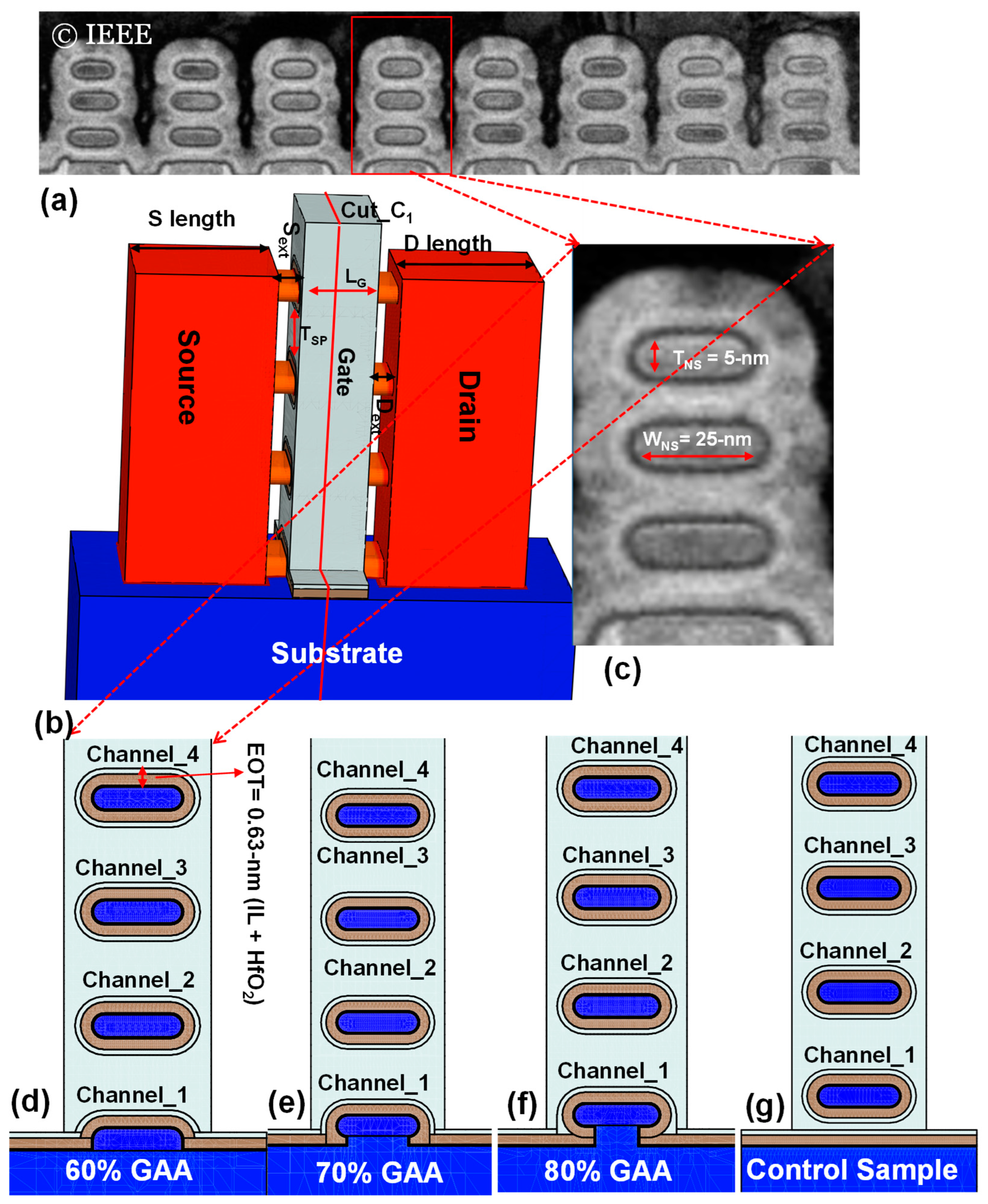
Figure 2.
Simulated ID-VG characteristics are presented for bulk NFETs and PFETs under (a) linear and (b) saturation drain bias conditions, with varying coverage ratios of the bottom parasitic leakage channel in the vertically stacked GAA NS device with bulk substrate. The leakage current of NFETs and PFETs are estimated for different coverage ratios of parasitic channels under (c) linear and (d) saturation drain bias conditions, respectively.
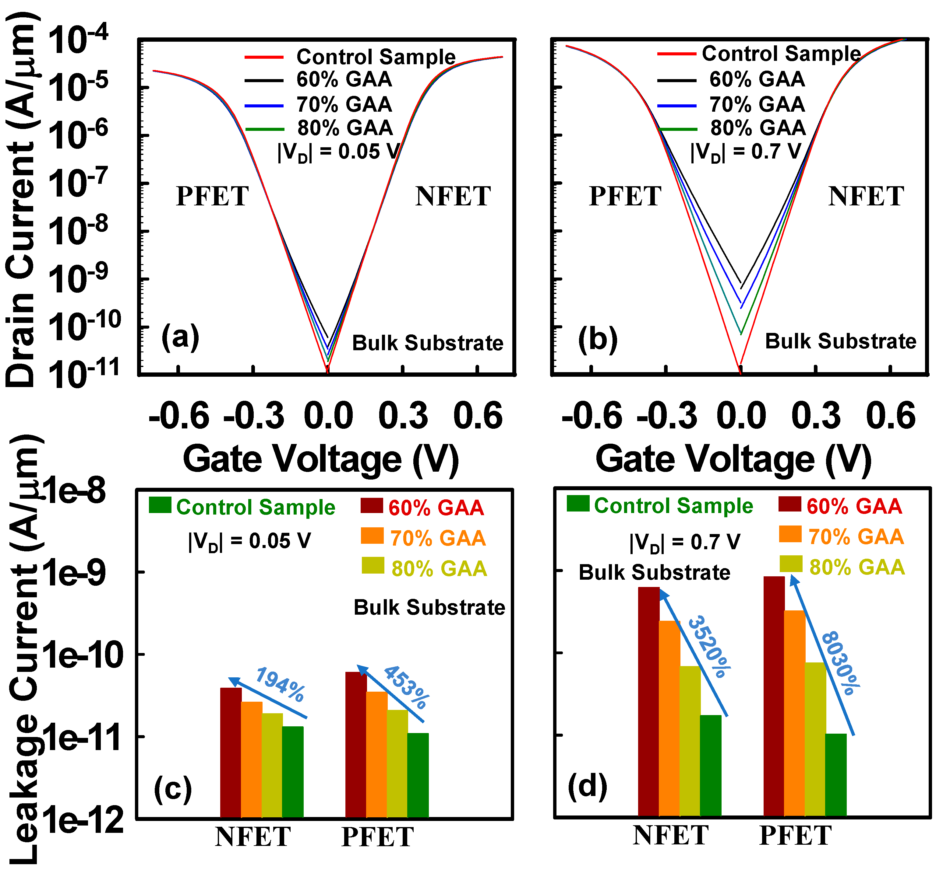
Figure 3.
For the device with bulk substrates, 2-D cross-sectional views of the off-state current density (VD = 0.7 V and VG = 0 V) distribution of NFETs are shown for the different bottom parasitic channel coverage ratios: (a) 60%, (b) 70%, (c) 80%, and (d) control sample (i.e., 100%), respectively.
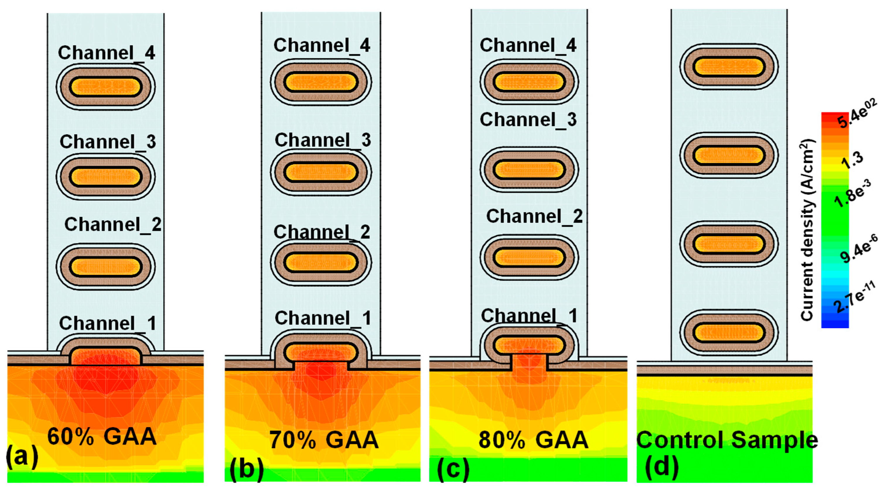
Figure 4.
Simulated ID-VG characteristics are presented for NFETs and PFETs under (a) linear and (b) saturation drain bias conditions, with varying coverage ratios of the bottom parasitic leakage channel in the vertically stacked GAA NS devices with SOI substrate. The leakage currents of NFETs and PFETs are estimated for different coverage ratios of parasitic channels under (c) linear and (d) saturation drain bias conditions.
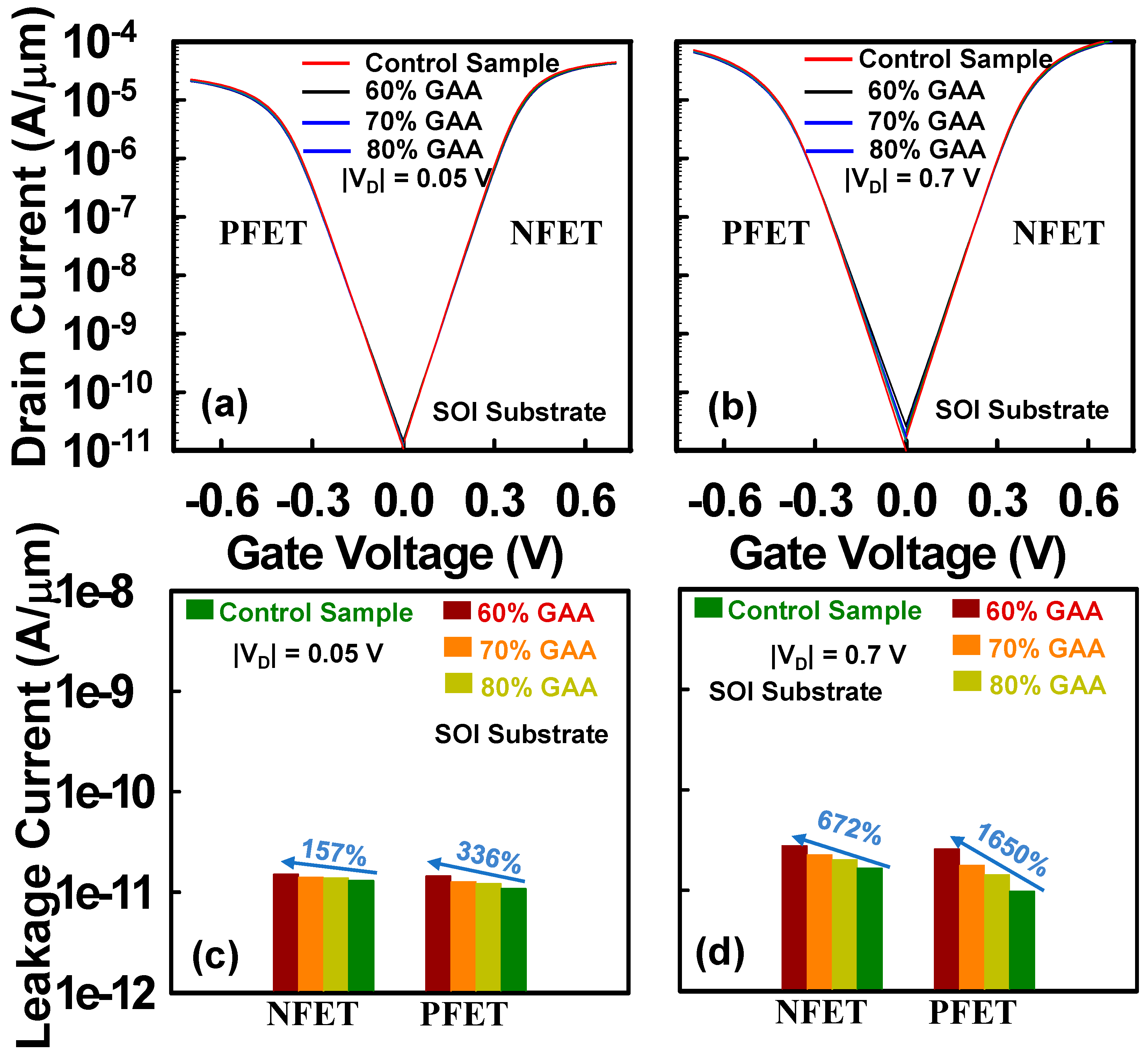
Figure 5.
For the device with SOI substrates, 2-D cross-sectional views of the off-state (VD = 0.7 V and VG = 0 V) current density distribution of NFETs are shown for the different bottom parasitic channel coverage ratios: (a) 60%, (b) 70%, (c) 80%, and (d) control (i.e., 100%), respectively.
Figure 5.
For the device with SOI substrates, 2-D cross-sectional views of the off-state (VD = 0.7 V and VG = 0 V) current density distribution of NFETs are shown for the different bottom parasitic channel coverage ratios: (a) 60%, (b) 70%, (c) 80%, and (d) control (i.e., 100%), respectively.

Figure 6.
The simulated ID-VD characteristics of NFETs and PFETs under the different coverage ratios of bottom parasitic channels: (a) bulk- and (b) SOI-substrate devices.
Figure 6.
The simulated ID-VD characteristics of NFETs and PFETs under the different coverage ratios of bottom parasitic channels: (a) bulk- and (b) SOI-substrate devices.
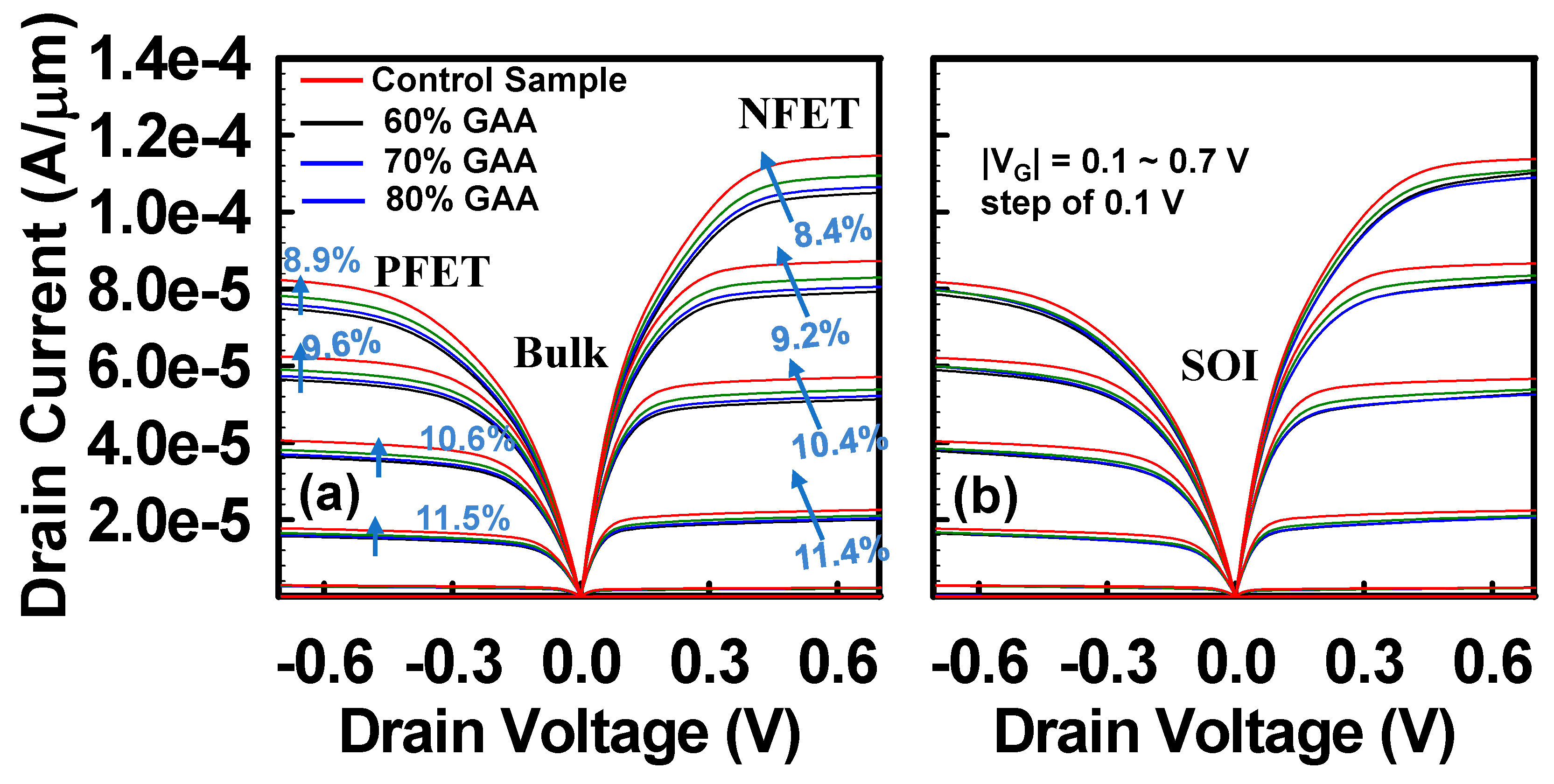
Figure 7.
The transconductance versus gate voltage of the different coverage ratios of bottom parasitic channels under the drain biasing of 0.7 V: (a) bulk and (b). SOI substrates.
Figure 7.
The transconductance versus gate voltage of the different coverage ratios of bottom parasitic channels under the drain biasing of 0.7 V: (a) bulk and (b). SOI substrates.
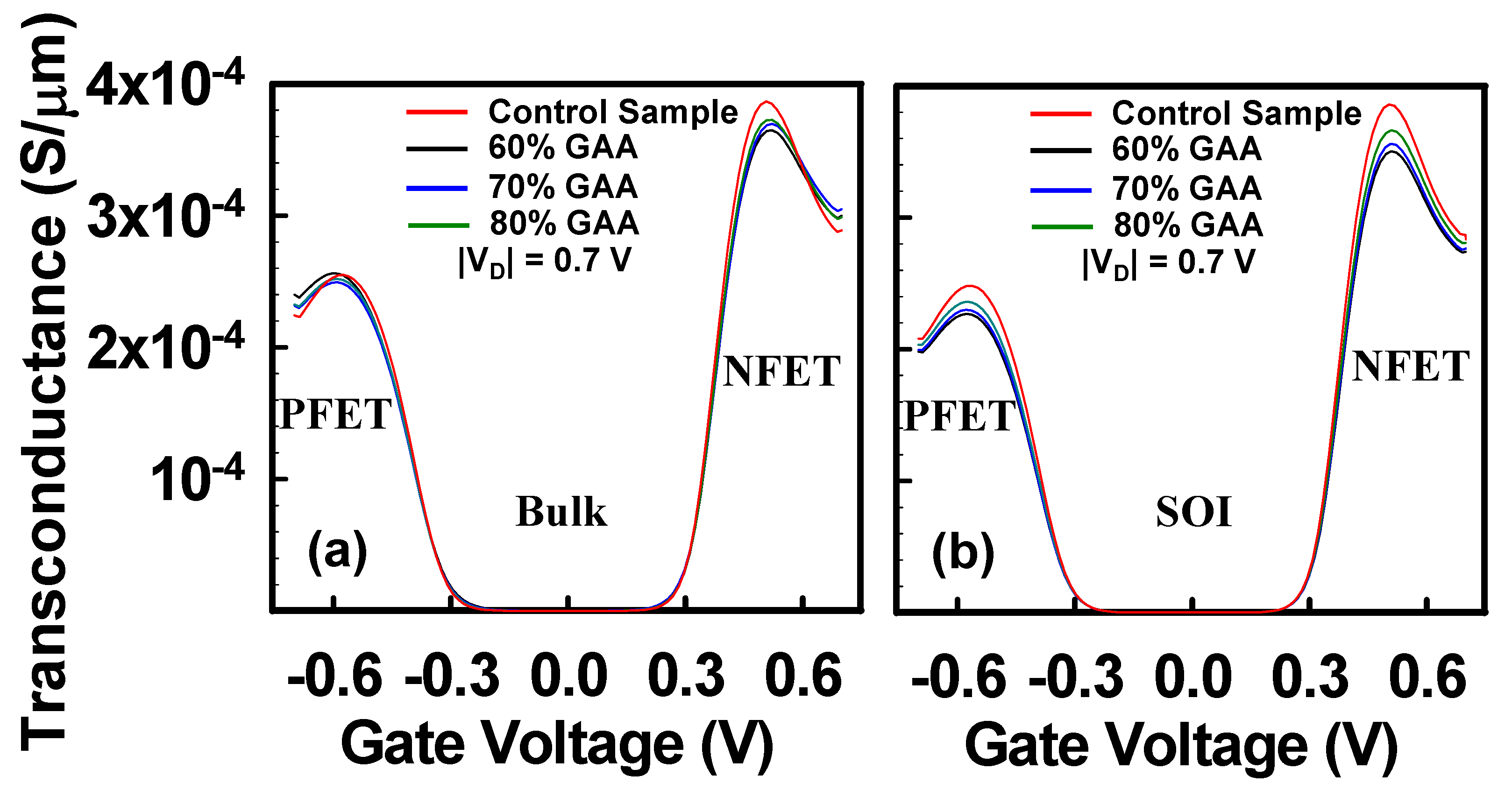
Figure 8.
The CG-VG characteristics among the different coverage ratios of bottom parasitic channels: (a) bulk and (b) SOI substrates.
Figure 8.
The CG-VG characteristics among the different coverage ratios of bottom parasitic channels: (a) bulk and (b) SOI substrates.
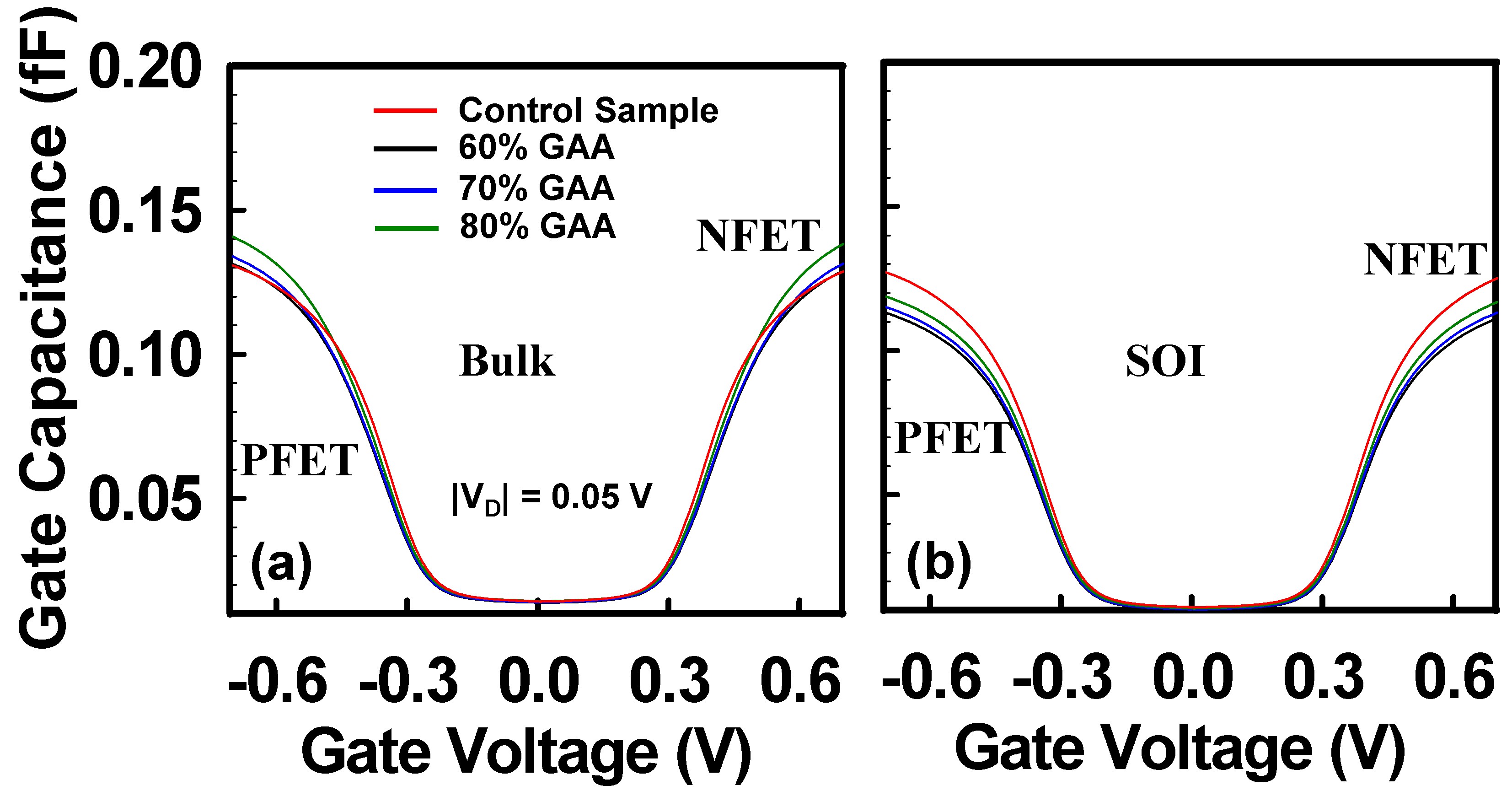
Figure 9.
The voltage gain versus frequency curves for different coverage ratios of bottom parasitic channels, the inset figure is the utilized common-source amplifier circuit for radio frequency (RF) simulations, where the value of R1 is 50 K, R2 is 50 K, and C is 10-6 F: (a) bulk and (b) SOI substrates. (c) The calculated 3-dB frequencies among different coverage ratios of bottom parasitic channels with bulk- and SOI-substrate devices. (d) The calculated cut-off frequency comparison between bulk- and SOI-substrate devices under the different coverage ratios of bottom parasitic channels.
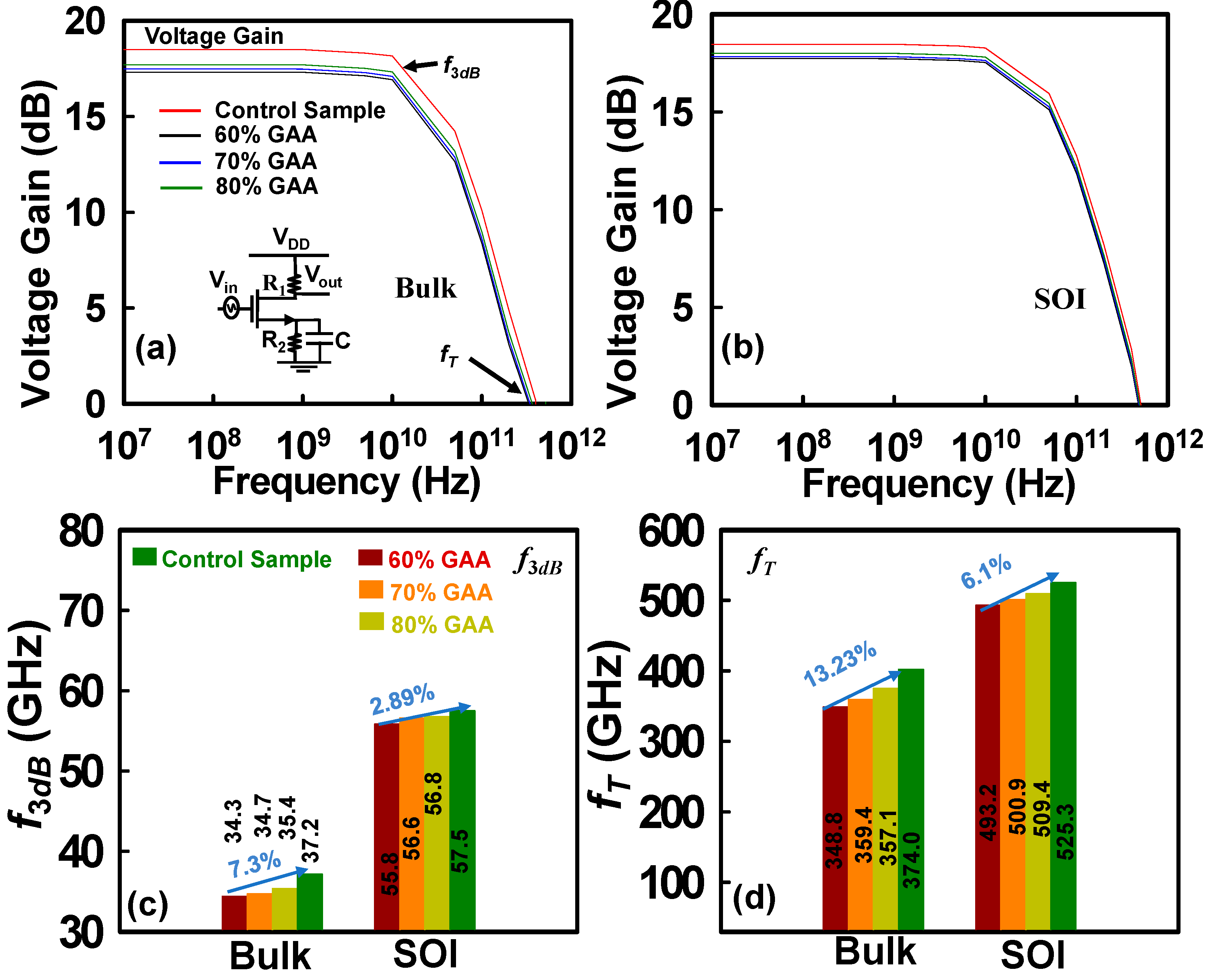
Figure 10.
(a)-(b) Input and output signals of the bulk-substrate CMOS inverter samples of different coverage ratios of bottom parasitic channels. Zoom-in plots of (c) high-to-low (tHL), rise time (tr) and (d) low-to-high (tLH), fall time (tf) timings under the two operations (NFET on and PFET off, NFET off and PFET on) conditions, respectively. (e) The comparison of timings of the different coverage ratios of bottom parasitic channels.
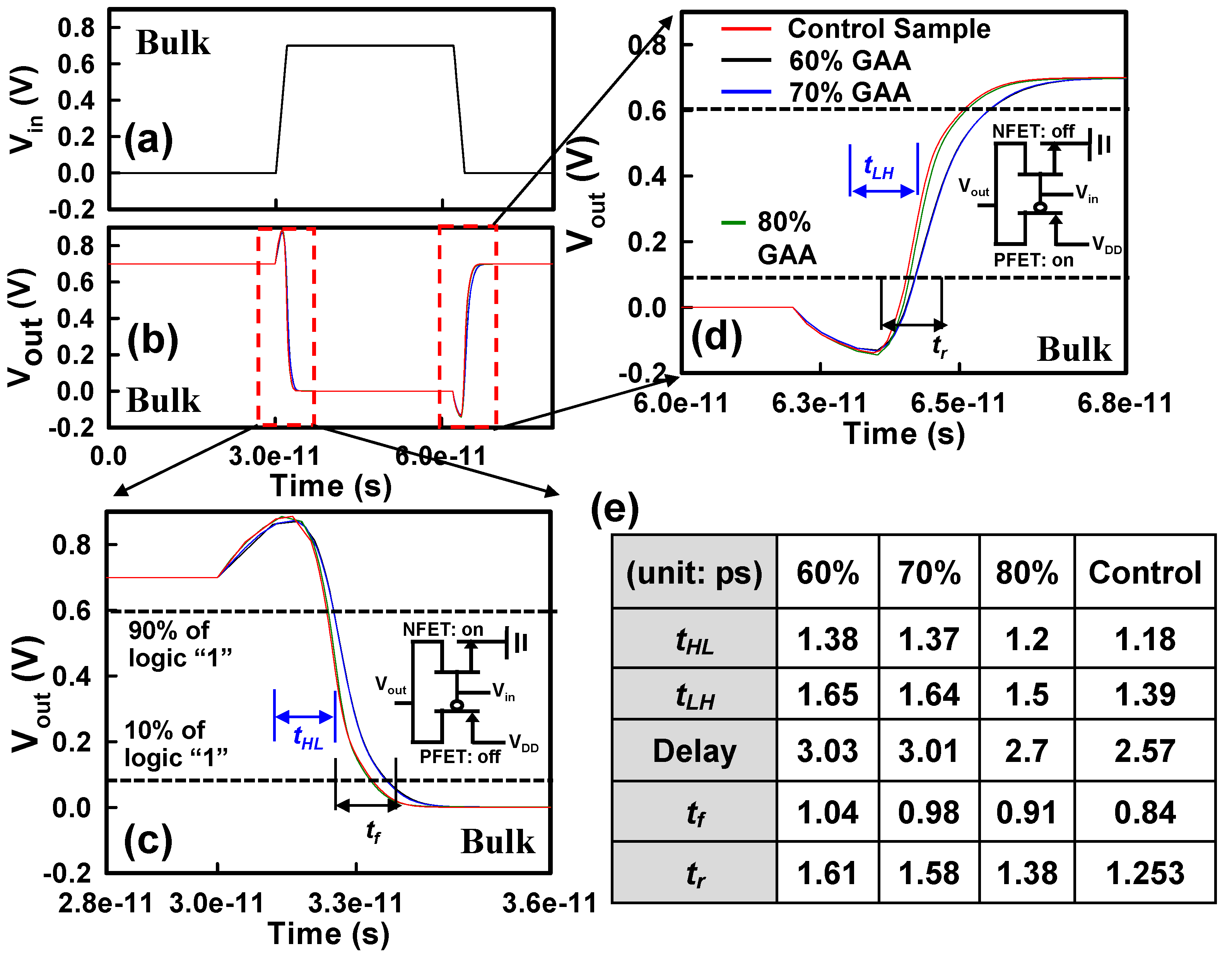
Figure 11.
(a)-(b) Input and output signals of the SOI-structure CMOS inverter samples of different coverage ratios of bottom parasitic channels. Zoom-in plots of (c) tHL, tr and (d) tLH, tf timings under the two operations (NFET on and PFET off, NFET off and PFET on) conditions, respectively. (e) The comparison of timings of the different coverage ratios of bottom parasitic channels.
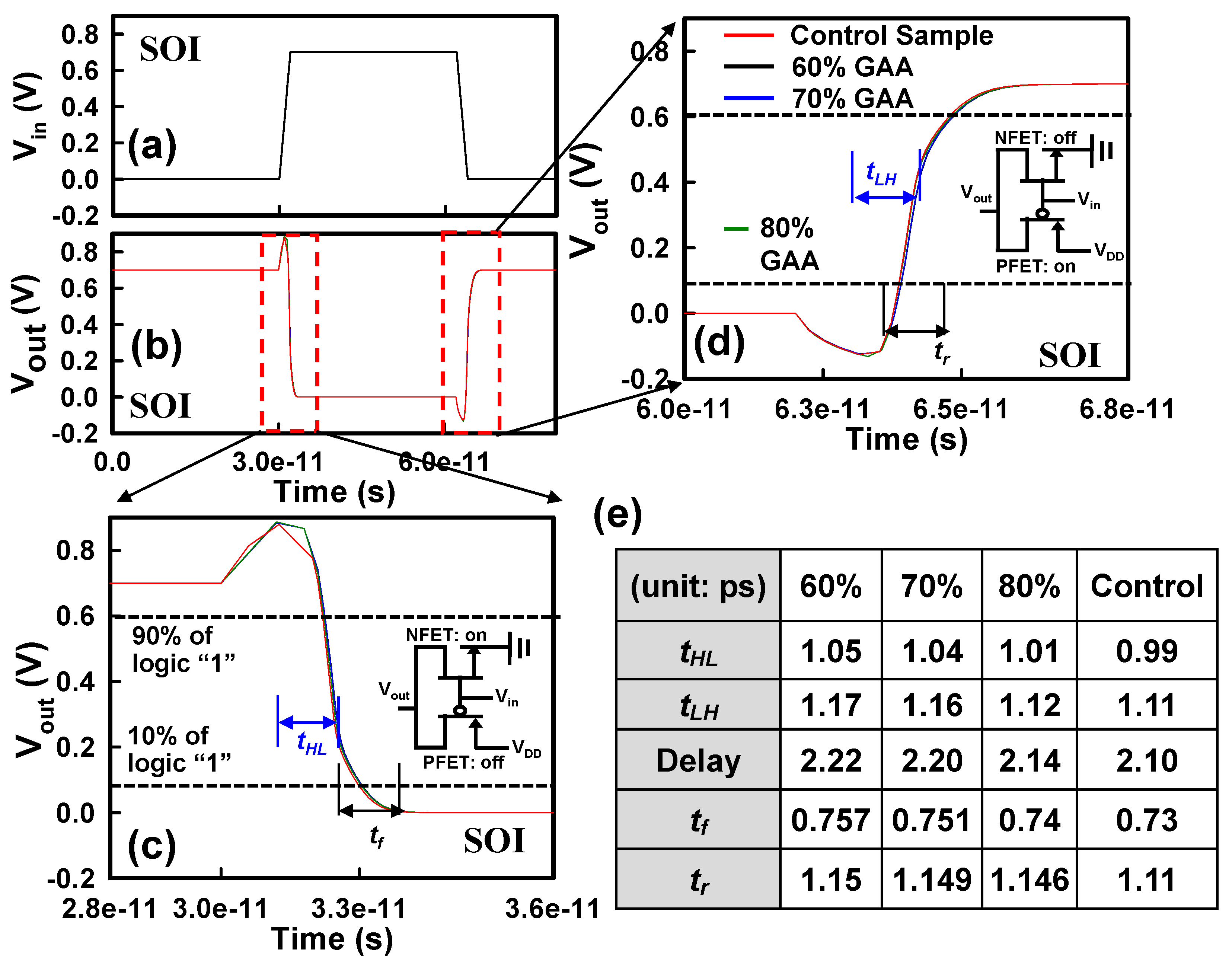
Figure 12.
The calculated static power, short-circuit power, dynamic power, and total power of GAA NS Si CMOS devices for different coverage ratios of bottom parasitic channels: (a) bulk- and (b) SOI-substrate devices.
Figure 12.
The calculated static power, short-circuit power, dynamic power, and total power of GAA NS Si CMOS devices for different coverage ratios of bottom parasitic channels: (a) bulk- and (b) SOI-substrate devices.


Table 1.
List of the adopted parameters of 60% coverage sample of GAA NS device and the achieved DC/AC/RF characteristics.
Table 1.
List of the adopted parameters of 60% coverage sample of GAA NS device and the achieved DC/AC/RF characteristics.
| Device parameter | Value |
| Channel length (nm) (LG) | 16 |
| Channel doping (cm-3) | 1 x 10¹⁵ |
| S/D extension (nm) | 5 |
| S/D length | 12 |
| Effective oxide thickness (nm) (EOT) | 0.63 |
| Nanosheet thickness (nm) (TNS) | 5 |
| Nanosheet width (nm) (WNS) | 25 |
| Work function (eV) | 4.45, 4.82 |
| S/D doping (cm-3) | 1 x 10²⁰ |
| S/D extension doping (cm-3) | 4.8 x 10¹⁸ |
| The achieved characteristics of the 60% GAA device and intrinsic RF parameters of a common source amplifier | |
| Absolute value of Threshold voltage (Vth) (mV) 250 | |
| Off-state current (Ioff) (A/mm) | 6.3 x 10⁻¹⁰ |
| On-state current (Ion) (A/mm) | 6.43 x 10⁻⁶ |
| Gate capacitance (CG) (fF) | 0.13 |
| Voltage gain (dB) | 17.3 |
| 3-dB frequency (f3dB) (GHz) | 34.5 |
| Cut-off frequency (fT) (GHz) | 348 |
Disclaimer/Publisher’s Note: The statements, opinions and data contained in all publications are solely those of the individual author(s) and contributor(s) and not of MDPI and/or the editor(s). MDPI and/or the editor(s) disclaim responsibility for any injury to people or property resulting from any ideas, methods, instructions or products referred to in the content. |
© 2023 by the authors. Licensee MDPI, Basel, Switzerland. This article is an open access article distributed under the terms and conditions of the Creative Commons Attribution (CC BY) license (http://creativecommons.org/licenses/by/4.0/).
Copyright: This open access article is published under a Creative Commons CC BY 4.0 license, which permit the free download, distribution, and reuse, provided that the author and preprint are cited in any reuse.


