
Submitted:
31 August 2023
Posted:
04 September 2023
You are already at the latest version
Abstract
The crystallization conditions from the solution play an important role in determining the mor-phology, phase composition, and photovoltaic properties of perovskite films. Post-processing of the obtained films can have a crucial role in increasing the grain size of perovskite and enhancing its crystallinity. It has been shown that the formation of crystal nuclei can be utilized to accelerate crystallization. In this case, crystallization occurs through the growth of seed crystals created in the solution, enabling the formation of relatively large crystals.
For the deposition of CH3NH3PbI3 hybrid halide perovskite films from a solution of the perovskite in dimethylformamide the spin coating echnique was employed. Pre-crystallization was achieved by heating films at a temperature of 100 or 110 °C. The dissolution process involved adding a drop of dimethylformamide onto the substrate surface and allowing it to partially dis-solve the perovskite for 30-40 seconds. Subsequently, residual solvent was removed through spin coating. The recrystallization process was carried out by heating films at the temperature range of 80 to 130 °C.
The morphological analysis of the perovskite film surfaces after recrystallization at tem-peratures ranging from 80 to 130 °C was performed. The infrared transmission spectra of the obtained perovskite films were investigated, and their light absorption characteristics were studied through transmission spectra. The perovskite structure in the obtained films was con-firmed by the peaks observed in the X-ray diffraction patterns.
Keywords:
Hybrid halide perovskites
; crystallization
; grain structure
; crystal nucleation
; crystal growth
1. Introduction
One of the main methods for obtaining hybrid perovskite films with a crystalline structure is the growth of crystals by heating the solution[1,2,3,4,5,6,7]. The morphology of perovskitefilm crystals obtained by the solution method is determined by the composition of the solution, the type of solvent, the method, and the conditions of crystallization[8,9].This method allows producing perovskite films with a crystalline structure in a single stage. Its implementation is achieved by the crystallization of concentrated solution (1.0-1.4 M) of hybrid perovskites in aprotic solvents such as dimethyl sulfoxide(DMSO) and dimethylformamide (DMF)[
10]. At the same time, the production and crystallization of hybrid perovskites is a complex multi-stage process, involving the formation of intermediate phases, such as crystal solvates [10], and their subsequent decomposition. For example, dimethylformamide can form a crystal solvate type PbI2*DMF with lead iodide [11], or form crystal solvates MAPbI3*DMF [12]. The crystallization of MAPbI3 from DMF leads to the formation of an intermediate phase, indicated by the light-yellow color of the crystallization product [13]. The presence of crystal solvates in the solution leads to the formation of needle crystals during crystallization, which results in incomplete coverage of the substrate surface. This significantly complicates the task of obtaining a perfect perovskite crystal structure on the substrate.
Currently, various technological approaches have been proposed to improve the morphology of perovskite films[9,14,15,16,17,18,19,20]. Their application during the crystallization of perovskite solutions can induce rapid nucleation processes. It has been established that the addition of anti-solvent makes it possible to obtain uniform perovskite films with a high degree of crystallinity from DMSO and DMF/DMSO solutions [9,17,18].For instance, one such approach is the deposition of the solution at an elevated temperature onto a preheated substrate. Another approach that can be utilized for this purpose is the anti-solvent method. In this case, immediately after obtaining the perovskite film from the solution, it is further treated with a solvent. As a result, a thin liquid layer consisting of a mixture of solvents forms on the film's surface, which promotes rapid nucleation of the crystal solvate phase [17,19]. Annealing the film at a temperature of 100-150 °C leads to the decomposition of the crystal solvate, followed by uniform crystallization of the perovskite [17,19].
The aforementioned information demonstrates that the crystallization conditions from the solution play a crucial role in determining the morphology, phase composition, and photoelectric properties of perovskite films. Therefore, a significant research direction in the field of hybrid perovskites is the search for conditions and processing regimes that enable the production of perovskite films with large grain sizes [9,21]. This is particularly relevant for obtaining perovskite films with a high degree of crystallinity [9,17,18,22].For instance, it has been shown in [9] that annealing the films in solvent vapors leads to an increase in grain size. However, the post-treatment regimes that can improve the crystal structure of perovskite films are still poorly understood at present.
2. Materials and Methods
The spin-coating method was used to deposit hybrid halide perovskite films onto substrates using a 30% solution of perovskite in dimethylformamide (DMF). In the case of the solution-based method, the choice of solvent for the organic and inorganic components determines characteristics such as morphology, crystallization process, thickness, and homogeneity of the perovskite films. Therefore, the physical parameters of the solvent significantly influence the formation of perovskite films.Table 1 presents the main physical parameters of the DMF solvent [9].
Slides made of regular silicate glass (25.4×76.2 mm²) were used as substrates, from which samples measuring 2.0×2.0 mm² were cut. The glass substrates with a layer of FTO (fluorine-doped tin oxide)were washed with water containing a surfactant. To remove grease contamination from the glass, they were treated with isopropyl alcohol heated to 60°C, followed by rinsing with distilled water and air-drying at 70°C. Prior to applying the perovskite film, the glass substrates were additionally treated with acetone dried with calcium chloride.
The overall scheme of the process for obtaining and crystallizing the hybrid halide perovskite film with the CH3NH3PbI3 compositionis presented in Figure 1. Excess perovskite solution was removed during substrate rotation.
After the pre-treatment operation, we proceeded to the deposition of the perovskite solution onto the substrate. To do this, a threefold mass excess of lead iodide powder dissolved in DMF was added to the solution containing methylammonium iodide(molar ratioMAI/PbI2=1:1). Prior to the deposition, the glass substrates were placed on a preheated centrifuge table at 90°C, and then a drop of concentrated solution of methylammoniumtriiodide lead (MAPbI3) in DMF was applied to the center of the glass sample. A centrifuge model SPIN-1200T (MIDASSYSTEM, Korea) was used for film deposition. Heating and annealing of the samples were performed using an ND-1A laboratory hotplate (Japan). During the experiments, nitrogen gas was supplied to the centrifuge box, and the centrifuge table was rotated at a speed of 600 revolutions per minute for 1 minute in a nitrogen atmosphere.
The crystallization process was carried out by annealingat temperatures of 80, 90, 100, 110, 120, and 130°C for 20 minutes in a nitrogen atmosphere. In the next step, a drop of DMF was added to the substrate and left for 30-40 seconds for partial dissolution of the perovskite layer. After that, the sample was placed on the centrifuge table and rotated at a speed of 600 revolutions per minute for 20 seconds. The obtained samples were then annealed at temperatures of 100 and 110°C.
The surface morphology of the MAPbI3films after crystallization was examined using an optical microscope "POLAM-R-312" (LOMO, Russia) with a video camera at a magnification of 500 times. The crystallization process of the CH3NH3PbI3 perovskite material was accompanied by the formation of a granular film structure with a color change from yellow to dark grayish-yellow.
X-ray phase analysis of the obtained perovskite film was performed using a high-resolution "UltimaIV" Rigaku X-ray diffractometer (Japan) with a CuKα line source. The operating parameters of the X-ray source were set at an accelerating voltage of 40 kV and a tube current of 30 mA. The measurement parameters were as follows: angle interval 2θ = 5–60°, scanning speed 5.0°/min.
The transmittance spectra of the perovskite films were measured using a PE-5400UV spectrophotometer with a spectral slit width of 4.0 nm.
Planar perovskite cells with the FTO/NiOx/CH3NH3PbI3/TiO2/Al structure, protected on both sides by glass, were applied for solar cell fabrication (Fig. 2). TiOx electron transport layer was formed by anodization of thin Ti layer on aluminum. NiOx hole transport layer was deposited by vacuum sputtering.
The photocurrent curves were collected in air with a Keithley 2400 source meter under simulated irradiation (100 mW/cm2) generated by a solar simulator.
3. Resultsand Discussion
One way to accelerate crystallization can be the preliminary formation of crystal nuclei. In this case, crystallization occurs through the growth of nucleated crystals in the solution, allowing for the formation of relatively large crystals.
Several studies have shown that the optimal annealing temperature for perovskite crystallization from a solution, resulting in a highly crystalline film, is about 110°C [8,11,23,24]. However, there is no available data in the literature regarding the optimal annealing temperature for re-crystallization (secondary crystallization) from a perovskite solution. Therefore, conducting experimental investigations to determine the optimal annealing temperature in the range of 80-150°C is of great interest. The obtained results of crystallization can contribute to an increase in the perovskite grain size and an increase in the crystallinity of the formed film.
Figure 3 shows the initial surface morphology of the perovskite film after crystallization from a perovskite solution with an annealing temperature of 110°C (pre-crystallization). As can be seen from Figure 3, after the initial annealing, the surface of the perovskite film exhibits the formation of individual crystal nuclei, which subsequently grow in size. The crystal grains have a round shape and are randomly distributed throughout the surface of the perovskite film. As a result, the film surface is not entirely covered with crystals.
Figure 4 presents the morphology images of the perovskitefilms (pre-annealed at 110°C) after partial dissolutionof perovskite surface in DMF and subsequent re-crystallization in the temperature range of 80 to 110°C. As evident from the obtained results, the re-crystallization process is accompanied by the growth of a large number of crystals.
To explain the influence of the annealing temperature on the perovskite solution, it is important to note that crystallization is accompanied by two main simultaneous processes: the formation of crystal nuclei and crystal growth.
The formation of crystal nuclei occurs through spontaneous crystallization. As seen in Figure 4, the annealing at 80 and 90 °C induces the formation of randomly shaped crystals. It can be assumed that an increase in annealing temperature leads to an increase in the crystal growth rate. If this rate is higher than the nucleation rate, it results in larger grain sizes. This is well illustrated in Figure 4 for samples annealed at 80 and 90 °C. On the other hand, during recrystallization with an annealing temperature of 110 °C, the formation of crystals with a uniform distribution over the entire film surface is observed. This indicates equilibrium between the processes of crystal growth and nucleation in the film, where the growth rate and nucleation rate are equal. Increasing the annealing temperature above 130 °C disrupts this equilibrium, resulting in a higher nucleation rate than the growth rate (Figure 5).
This should lead to the formation of a large number of nuclei and, consequently, the formation of small crystals. As seen in Figure 4, as the annealing temperature increases from 130 °C to 150 °C, the grain size significantly decreases, and the number of crystals increases. Table 2 presents the results of grain size determination for different annealing temperatures based on the data presented in Figure 4 and Figure 5.
Thus, the temperature of 110 °C, at which the growth rate of crystals and the nucleation rate are balanced in the formed perovskitefilm, is optimal for the crystallization of the perovskite solution. Annealing at this temperature makes it possible to form a granular structure in the perovskite film with the largest grain size and close-packed crystals over the entire surface of the film.
Figure 6 shows the results of the investigation of freshly prepared perovskite films using infrared (IR) spectroscopy. The IR spectrum of the obtained films indicates the presence of N-H and C-H bonds, confirming the presence of perovskite compounds. The most intense doublet peak in the perovskite film spectrum, with absorption maxima at 3132 and 3179 cm-1, can be attributed to the symmetric and asymmetric vibrations of N-H bonds, which are associated with NH3+. The characteristic vibrations of C-H bonds are also observed, with absorption frequencies at 2921 and 2951 cm-1 for symmetric and asymmetric vibrations, respectively.
The light absorption characteristics of the samples were investigated using transmission spectra. Figure 7 shows that the sample with a crystallization temperature of 110 °C exhibits better absorption in the visible range (400-700 nm) compared to the sample obtained at 130 °C. This result may be attributed to the improved crystallinity of the perovskite film in the sample with a crystallization temperature of 110 °C.
XRD characterization has been performed to identify the phases present in the synthesized films. The X-ray diffraction pattern of the CH3NH3PbI3 perovskite film after crystallization at T = 110 °C are shown in Figure 8. The peaks in the X-ray diffraction pattern (2θ: 14.12 (110), 28.41 (220) and 43.19 (330))indicate the formation of tetragonal perovskite structure of CH3NH3PbI3.
Investigation of the photoelectric properties of planar perovskite cells with the FTO/NiOx/CH3NH3PbI3/TiO2/Al structure, protected on both sides by glass, revealed that for the perovskite films obtained after re-crystallization, a current of approximately 20 mA/cm2 was generated at a voltage of 716 mV under an artificial light intensity of 100 mW/cm2. The photocurrent values for these samples were 15-20% higher compared to perovskite films obtained through conventional crystallization.
4. Conclusions
It has been shown that the conditions of crystallization from solution play a crucial role in determining the morphology and photoelectric properties of perovskite films.
To accelerate the crystallization process, the pre-formation of crystal nuclei has been proposed. In this approach, crystallization occurs through the growth of nuclei created in the solution, allowing the formation of relatively large crystals. It has been demonstrated that post-treatment of the obtained perovskite films through recrystallization can improve the crystal structure.
It is hypothesized that during the crystallization of perovskite film from the solution, two competing processes occur simultaneously: the formation of crystal nuclei and crystal growth which determine the morphology and crystal sizes of the formed films.It should be noted that the formation of nuclei occurs through spontaneous crystallization.In the case where the crystal growth rate exceeds the nucleation rate, the formation of randomly shaped crystals is observed (recrystallization with annealing temperature of 90 °C). When the rates of these two processes are equal, uniform distribution of crystals across the film surface takes place (recrystallization with annealing temperature of 110 °C). In the case of imbalance, with nucleation rate exceeding the crystal growth rate, the formation of small crystals occurs (recrystallization with annealing temperature of 130-150 °C). Thus, the temperature of 110 °C, at which the crystal growth and nucleation rates in the perovskite solution are balanced, is optimal for the recrystallization of the CH3NH3PbI3perovskite films.
Investigation of the photoelectric properties of planar perovskite cells with the structure FTO/NiOx/CH3NH3PbI3/TiO2/Al, protected on both sides by glass, has shown that the photocurrent values for perovskite films obtained through recrystallization were 15-20%higher than those of perovskite films obtained through conventional crystallization methods.
Author Contributions
Conceptualization, I. Vrublevsky; methodology, I. Vrublevsky, A. Aleshin and A. Tuchkovsky; software, N. Lushpa and A. Maksimov; validation, E. Muratova, V. Moshnikovand I. Vrublevsky; formal analysis, I. Vrublevsky and A. Tuchkovsky; investigation, N. Lushpa, G. Nenashev and A. Maksimov; resources, N. Lushpa and E. Muratova; data curation, E. Muratova; writing—original draft preparation I. Vrublevsky; writing—review and editing, E. Muratova; visualization, N. Lushpa; supervision, E. Muratova; project administration, V. Moshnikov; funding acquisition, V. Moshnikov All authors have read and agreed to the published version of the manuscript.
Funding
This research was funded by Belarusian Republican Foundation for Fundamental Research grant number F23RNF-160.
Acknowledgments
The study was supported by the Russian Science Foundation grant No. 23-42-10029, https://rscf.ru/en/project/23-42-10029/
Conflicts of Interest
The authors declare no conflict of interest.
References
- Saidaminov, M.I.; Abdelhady, A.L.; Murali, B.; Alarousu, E.; Burlakov, V.M.; Peng, W.; Dursun, I.; Wang, L.; He, Y.; MacUlan, G.; et al. High-Quality Bulk Hybrid Perovskite Single Crystals within Minutes by Inverse Temperature Crystallization. Nat. Commun.2015, 6, 7856. [CrossRef]
- Hamill, J.C.; Schwartz, J.; Loo, Y.L. Influence of Solvent Coordination on Hybrid Organic-Inorganic Perovskite Formation. ACS Energy Lett.2018, 3, 92–97. [CrossRef]
- Baikie, T.; Fang, Y.; Kadro, J.M.; Schreyer, M.; Wei, F.; Mhaisalkar, S.G.; Graetzel, M.; White, T.J. Synthesis and Crystal Chemistry of the Hybrid Perovskite (CH 3NH3)PbI3 for Solid-State Sensitised Solar Cell Applications. J. Mater. Chem. A2013, 1, 5628–5641. [CrossRef]
- Dunlap-Shohl, W.; Zhou, Y.; Padture, N.; Mitzi, D. Synthetic Approaches for Halide Perovskite Thin Films. Chem. Rev.2019, 119, 3193–3295.
- Stoumpos, C.C.; Malliakas, C.D.; Kanatzidis, M.G. Semiconducting Tin and Lead Iodide Perovskites with Organic Cations: Phase Transitions, High Mobilities, and near-Infrared Photoluminescent Properties. Inorg. Chem.2013, 52, 9019–9038. [CrossRef]
- Mitzi, D.B. Synthesis, Structure, and Properties of Organic-Inorganic Perovskites and Related Materials. In Progress in Inorganic Chemistry; 2007; Vol. 48, pp. 1–121.
- Aleksandrova, M.; Tomov, R.; Vrublevsky, I. Study of Lead-Free Perovskite Solar Cells at Elevated Temperatures and UV Irradiation. In Proceedings of the 2022 31st International Scientific Conference Electronics, ET 2022 - Proceedings; 2022; pp. 1–6.
- Jeon, N.J.; Noh, J.H.; Kim, Y.C.; Yang, W.S.; Ryu, S.; Seok, S. Il Solvent Engineering for High-Performance Inorganic-Organic Hybrid Perovskite Solar Cells. Nat. Mater.2014, 13, 897–903. [CrossRef]
- Cai, B.; Zhang, W.H.; Qiu, J. Solvent Engineering of Spin-Coating Solutions for Planar-Structured High-Efficiency Perovskite Solar Cells. Cuihua Xuebao/Chinese J. Catal.2015, 36, 1183–1190. [CrossRef]
- Gratia, P.; Zimmermann, I.; Schouwink, P.; Yum, J.H.; Audinot, J.N.; Sivula, K.; Wirtz, T.; Nazeeruddin, M.K. The Many Faces of Mixed Ion Perovskites: Unraveling and Understanding the Crystallization Process. ACS Energy Lett.2017, 2, 2686–2683. [CrossRef]
- Cao, J.; Jing, X.; Yan, J.; Hu, C.; Chen, R.; Yin, J.; Li, J.; Zheng, N. Identifying the Molecular Structures of Intermediates for Optimizing the Fabrication of High-Quality Perovskite Films. J. Am. Chem. Soc.2016, 138, 9919–9926. [CrossRef]
- Mitzi, D.B.; Liang, K. Synthesis, Resistivity, and Thermal Properties of the Cubic Perovskite NH2CH=NH2SnI3and Related Systems. J. Solid State Chem.1997, 134, 376–381.
- Mao, W.; Zheng, J.; Zhang, Y.; Chesman, A.S.R.; Ou, Q.; Hicks, J.; Li, F.; Wang, Z.; Graystone, B.; Bell, T.D.M.; et al. Controlled Growth of Monocrystalline Organo-Lead Halide Perovskite and Its Application in Photonic Devices. Angew. Chemie - Int. Ed.2017, 56, 12660–12665. [CrossRef]
- Nie, W.; Tsai, H.; Asadpour, R.; Blancon, J.C.; Neukirch, A.J.; Gupta, G.; Crochet, J.J.; Chhowalla, M.; Tretiak, S.; Alam, M.A.; et al. High-Efficiency Solution-Processed Perovskite Solar Cells with Millimeter-Scale Grains. Science (80-. ).2015, 347, 522–525. [CrossRef]
- Chen, Y.; He, M.; Peng, J.; Sun, Y.; Liang, Z. Structure and Growth Control of Organic–Inorganic Halide Perovskites for Optoelectronics: From Polycrystalline Films to Single Crystals. Adv. Sci.2016, 3, 1500392. [CrossRef]
- Li, X.; Bi, D.; Yi, C.; Décoppet, J.D.; Luo, J.; Zakeeruddin, S.M.; Hagfeldt, A.; Grätzel, M. A Vacuum Flash-Assisted Solution Process for High-Efficiency Large-Area Perovskite Solar Cells. Science (80-. ).2016, 353, 58–62. [CrossRef]
- Park, N.G. Methodologies for High Efficiency Perovskite Solar Cells. Nano Converg. 2016, 3.
- Liu, J.; Gao, C.; He, X.; Ye, Q.; Ouyang, L.; Zhuang, D.; Liao, C.; Mei, J.; Lau, W. Improved Crystallization of Perovskite Films by Optimized Solvent Annealing for High Efficiency Solar Cell. ACS Appl. Mater. Interfaces2015, 7, 24008–24015. [CrossRef]
- You, P.; Li, G.; Tang, G.; Cao, J.; Yan, F. Ultrafast Laser-Annealing of Perovskite Films for Efficient Perovskite Solar Cells. Energy Environ. Sci.2020, 13, 1187–1196. [CrossRef]
- Lee, J.W.; Kim, H.S.; Park, N.G. Lewis Acid-Base Adduct Approach for High Efficiency Perovskite Solar Cells. Acc. Chem. Res.2016, 49, 311–319. [CrossRef]
- Petrov, A.A.; Tarasov, A.B. Methylammonium Polyiodides in Perovskite Photovoltaics: From Fundamentals to Applications. Front. Chem. 2020, 8, 418.
- Saliba, M.; Matsui, T.; Seo, J.Y.; Domanski, K.; Correa-Baena, J.P.; Nazeeruddin, M.K.; Zakeeruddin, S.M.; Tress, W.; Abate, A.; Hagfeldt, A.; et al. Cesium-Containing Triple Cation Perovskite Solar Cells: Improved Stability, Reproducibility and High Efficiency. Energy Environ. Sci.2016, 9, 1989–1997. [CrossRef]
- Tutantsev, A.S.; Udalova, N.N.; Fateev, S.A.; Petrov, A.A.; Petrov, A.A.; Chengyuan, W.; Maksimov, E.G.; Goodilin, E.A.; Goodilin, E.A.; Tarasov, A.B.; et al. New Pigeonholing Approach for Selection of Solvents Relevant to Lead Halide Perovskite Processing. J. Phys. Chem. C2020, 124, 11117–11123. [CrossRef]
- Rong, Y.; Venkatesan, S.; Guo, R.; Wang, Y.; Bao, J.; Li, W.; Fan, Z.; Yao, Y. Critical Kinetic Control of Non-Stoichiometric Intermediate Phase Transformation for Efficient Perovskite Solar Cells. Nanoscale2016, 8, 12892–12899. [CrossRef]
Figure 1.
The overall scheme of the process for obtaining and crystallizing a film of CH3NH3PbI3 hybrid halide perovskite.
Figure 1.
The overall scheme of the process for obtaining and crystallizing a film of CH3NH3PbI3 hybrid halide perovskite.
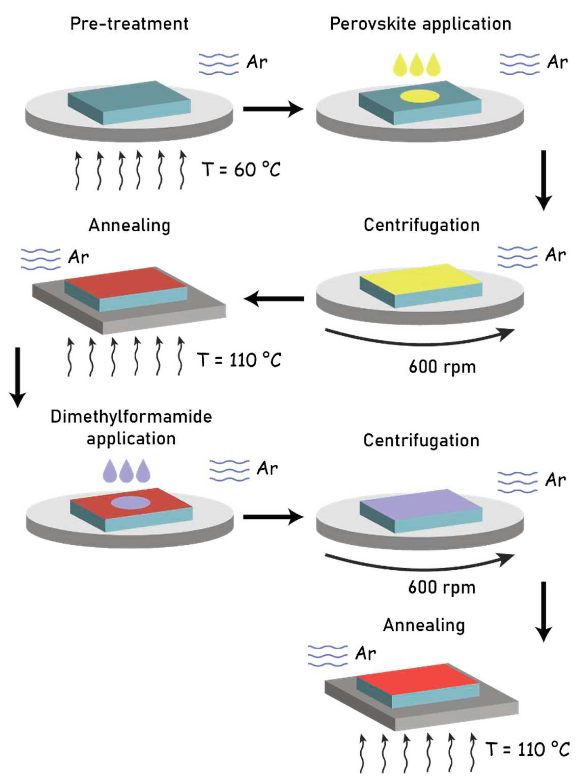
Figure 2.
Schematicmultilayer structure of planar perovskite solar cell.
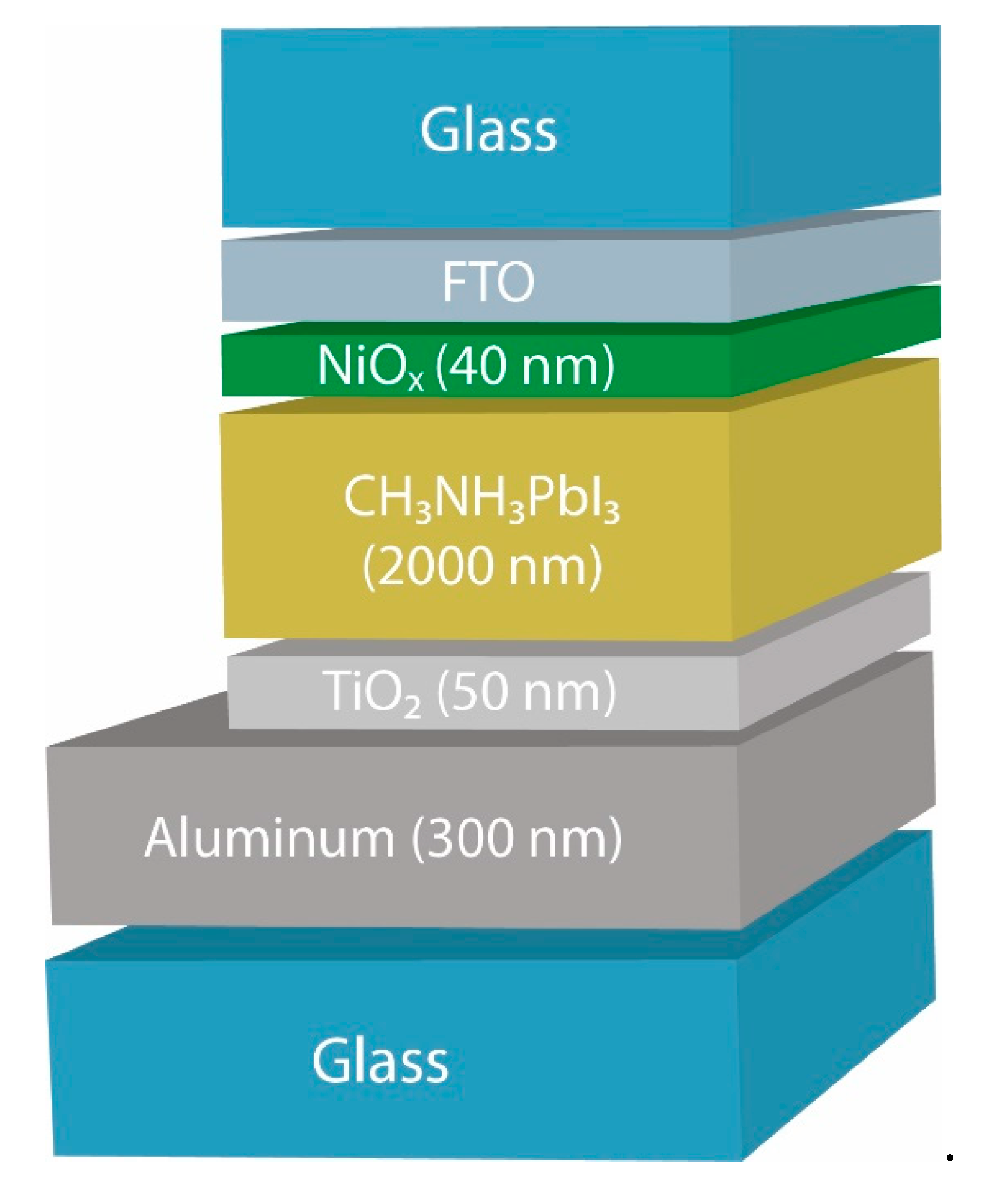
Figure 3.
Initial morphology of the surface of the perovskite film after crystallization from a perovskite solution with annealing temperature of 110°C (pre-crystallization).
Figure 3.
Initial morphology of the surface of the perovskite film after crystallization from a perovskite solution with annealing temperature of 110°C (pre-crystallization).
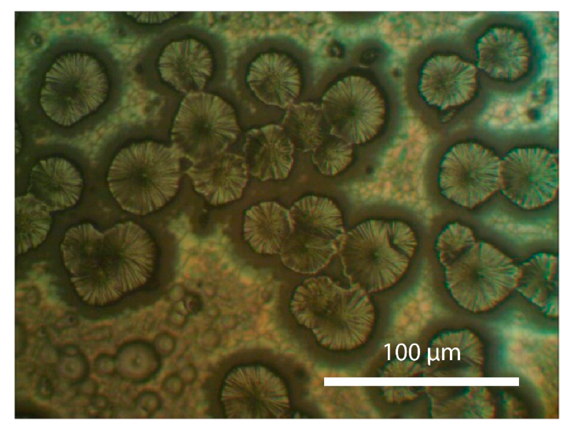
Figure 4.
Morphology of perovskite films (pre-annealing at 110 °C) afterpartial dissolutionof the perovskite surface in dimethylformamide and subsequent recrystallization in the temperature range of 80 to 110 °C. a - at 80 °C, b - at 90 °C, c - at 100 °C, d - at 110 °C.
Figure 4.
Morphology of perovskite films (pre-annealing at 110 °C) afterpartial dissolutionof the perovskite surface in dimethylformamide and subsequent recrystallization in the temperature range of 80 to 110 °C. a - at 80 °C, b - at 90 °C, c - at 100 °C, d - at 110 °C.
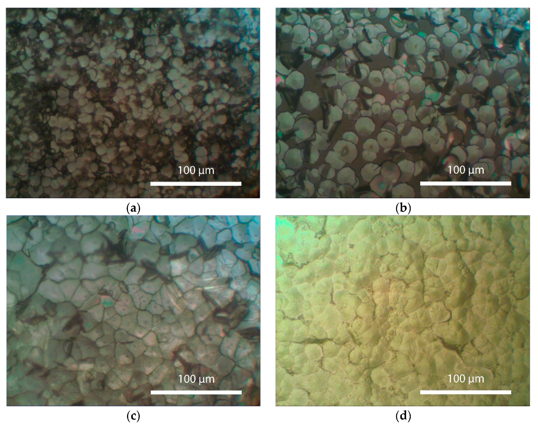
Figure 5.
Morphology of perovskite films (pre-annealing at 110 °C) after partial dissolutionof the perovskitesurface in dimethylformamide and subsequent recrystallization in the temperature range of 120 to 150 °C. a - at 120 °C, b - at 130 °C, c - at 140 °C, d - at 150 °C.
Figure 5.
Morphology of perovskite films (pre-annealing at 110 °C) after partial dissolutionof the perovskitesurface in dimethylformamide and subsequent recrystallization in the temperature range of 120 to 150 °C. a - at 120 °C, b - at 130 °C, c - at 140 °C, d - at 150 °C.
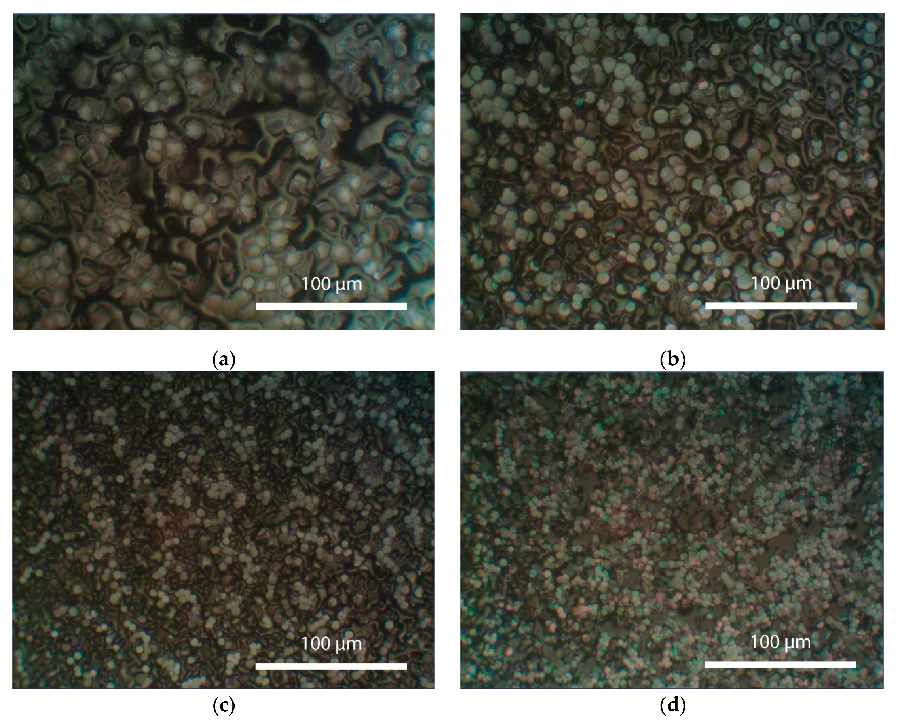
Figure 6.
IR transmittance spectra of the CH3NH3PbI3 perovskite films after crystallization at an annealing temperature of 110 °C and 130 °C.
Figure 6.
IR transmittance spectra of the CH3NH3PbI3 perovskite films after crystallization at an annealing temperature of 110 °C and 130 °C.
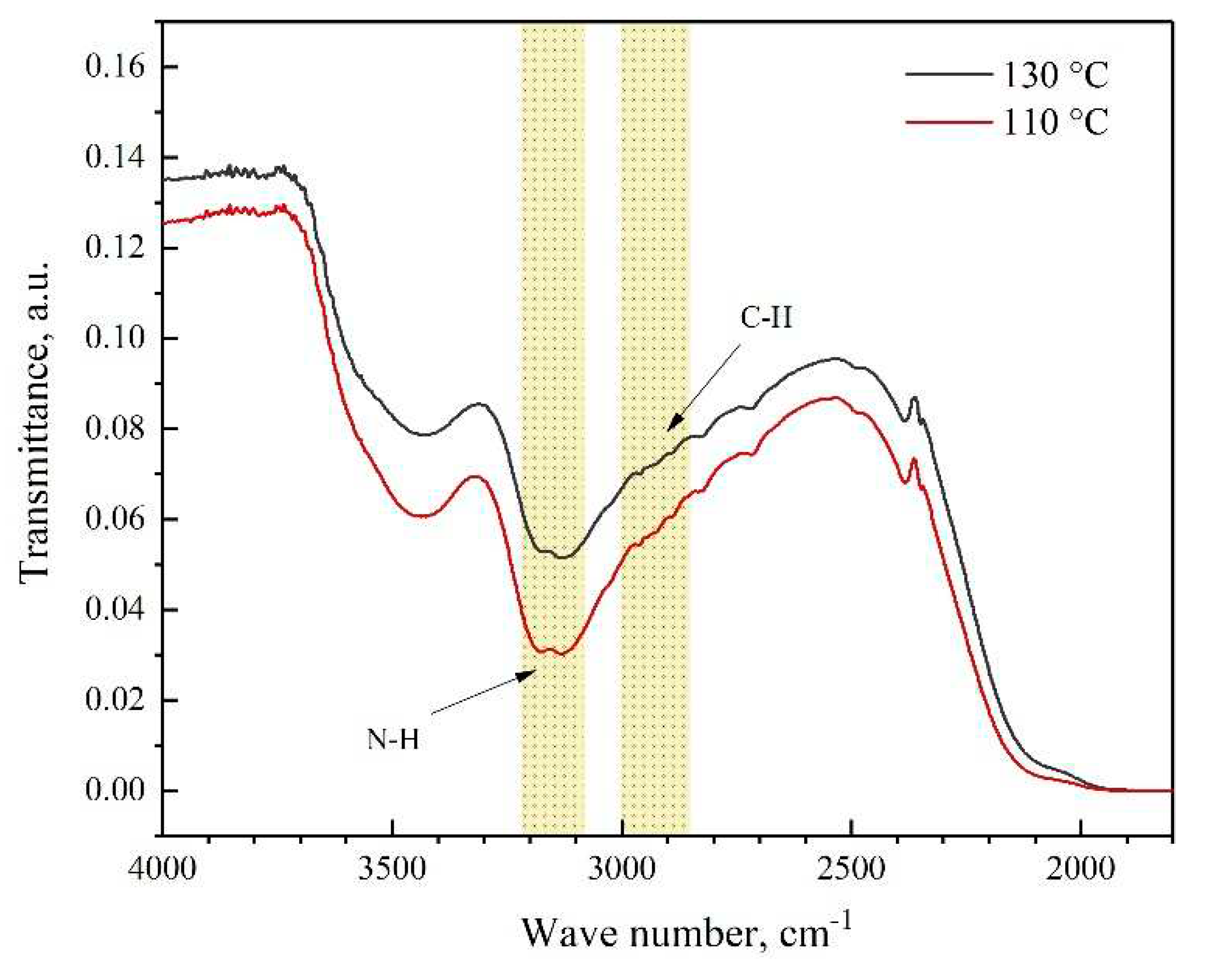
Figure 7.
Transmittance spectra in the visible region of the CH3NH3PbI3perovskite films after crystallization at annealing temperatures of 110 °C and 130 °C.
Figure 7.
Transmittance spectra in the visible region of the CH3NH3PbI3perovskite films after crystallization at annealing temperatures of 110 °C and 130 °C.
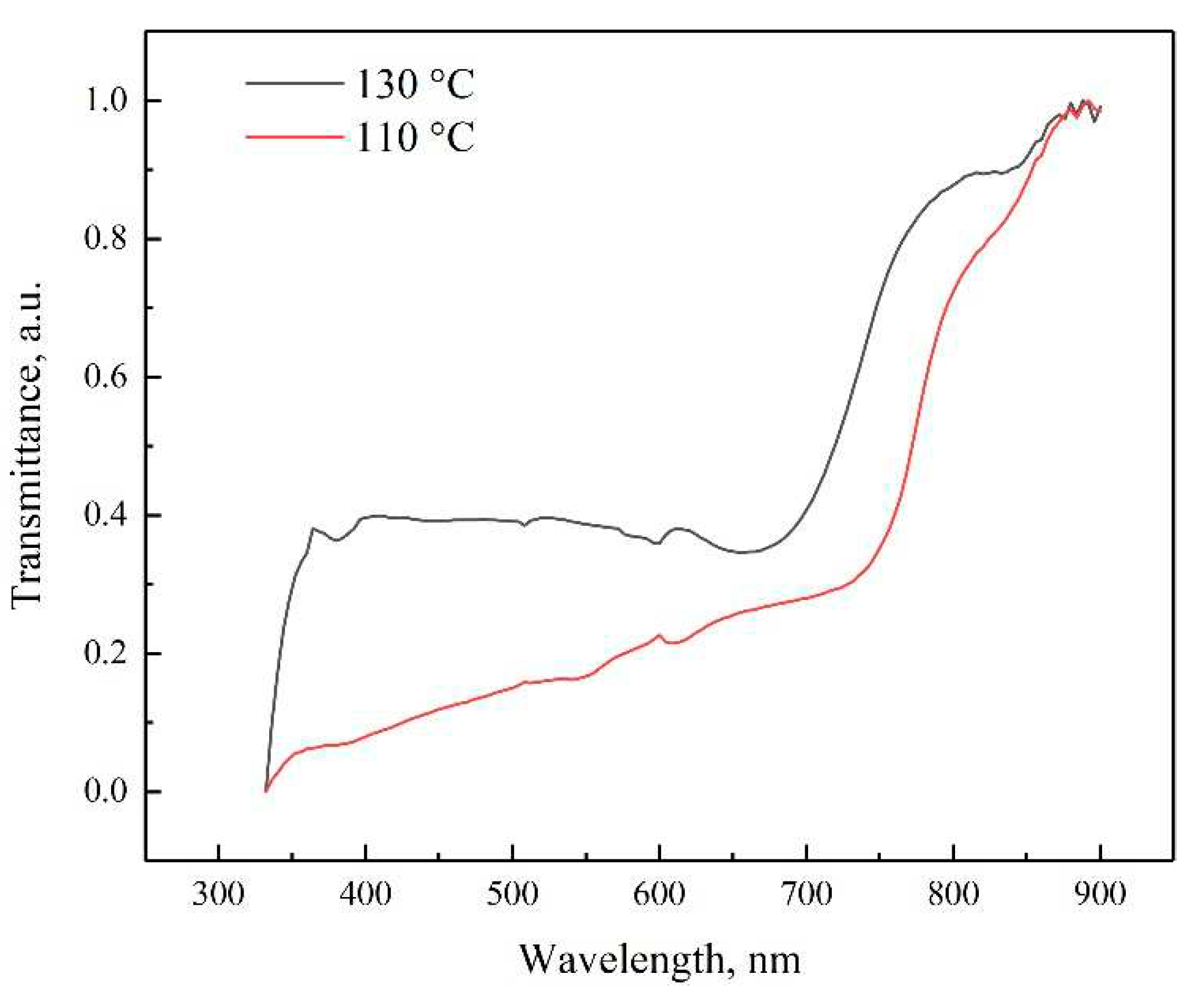
Figure 8.
X-ray diffraction pattern of the CH3NH3PbI3 perovskite film after crystallization at T = 110 °C.
Figure 8.
X-ray diffraction pattern of the CH3NH3PbI3 perovskite film after crystallization at T = 110 °C.
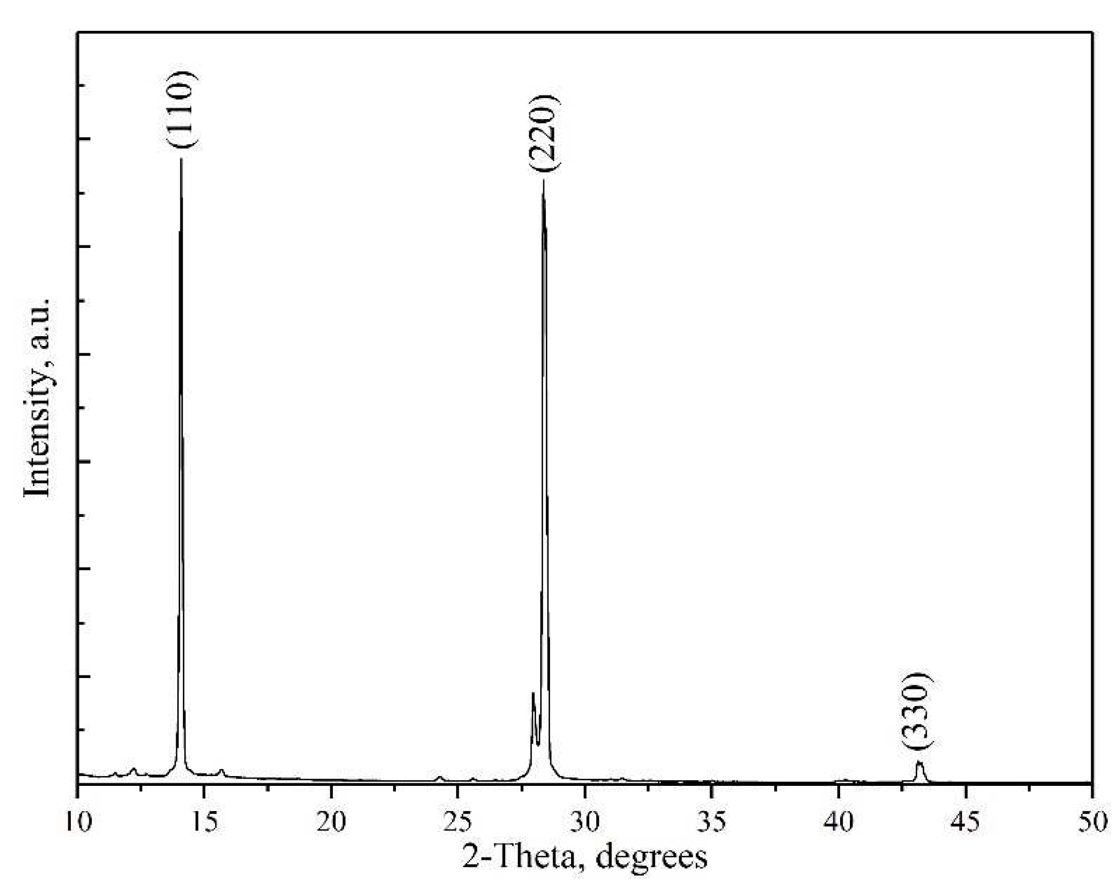

Table 1.
Main physical parameters of the DMF solvent [9].
Table 1.
Main physical parameters of the DMF solvent [9].
| Solvent | Boiling Point, °C | Vapor Pressure, mmHg (20 °C) | Density, g/mL (25 °C) | Viscosity, mPa‧s (25 °C) |
|---|---|---|---|---|
| DMF | 153 | 2.70 | 0.9445 | 0.8 |
Table 2.
Average grain sizes of perovskite film crystals after recrystallization for different annealing temperatures.
Table 2.
Average grain sizes of perovskite film crystals after recrystallization for different annealing temperatures.
| Annealing Temperature, °C | Average Grain Diameter, μm |
|---|---|
| 80 | 12.7 |
| 90 | 20 |
| 100 | 31.5 |
| 110 | 32.0 |
| 120 | 14.5 |
| 130 | 9.9 |
| 140 | 5.0 |
| 150 | 4.8 |
Disclaimer/Publisher’s Note: The statements, opinions and data contained in all publications are solely those of the individual author(s) and contributor(s) and not of MDPI and/or the editor(s). MDPI and/or the editor(s) disclaim responsibility for any injury to people or property resulting from any ideas, methods, instructions or products referred to in the content. |
© 2023 by the authors. Licensee MDPI, Basel, Switzerland. This article is an open access article distributed under the terms and conditions of the Creative Commons Attribution (CC BY) license (http://creativecommons.org/licenses/by/4.0/).
Copyright: This open access article is published under a Creative Commons CC BY 4.0 license, which permit the free download, distribution, and reuse, provided that the author and preprint are cited in any reuse.


