Submitted:
02 August 2023
Posted:
03 August 2023
Read the latest preprint version here
Abstract
Vertical III-V semiconductor nanowires have shown promising absorption of light for solar cell and photodetector applications. The absorption properties can be tuned through the choice of III-V materials and geometry of the nanowires. Here, we review recent progress in the design of the absorption properties of both individual nanowires and nanowire arrays. Future directions for the research field are proposed.
Keywords:
III-V semiconductor
; nanowire
; absorption
; solar cell
; photodetector
1. Introduction
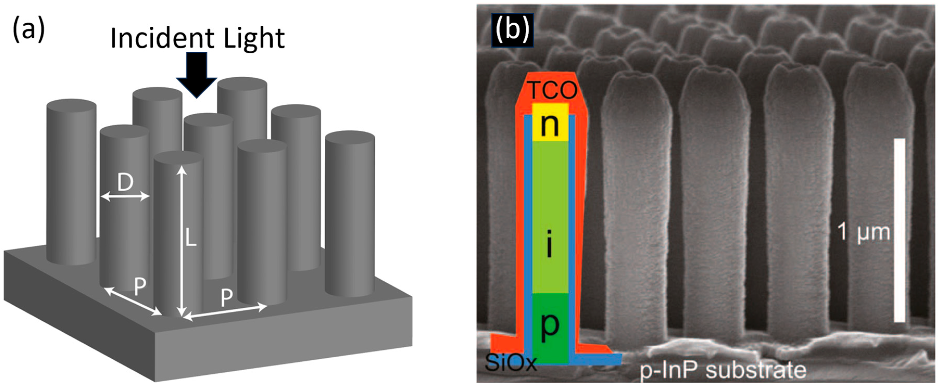
III-V semiconductors (III-Vs) allow for large tuneability for absorption-based applications through the choice of III-Vs used [1]. In the form of nanowires (see Figure 1), the optical response, including the absorption of light, can be further tuned through geometry design [2]. This combination of materials and geometry tuning make III-V nanowires highly interesting for solar cells and photodetectors [3,4,5,6,7,8].
Figure 1.
(a) Schematic of a nanowire array with nanowires of diameter and length in a square array of period . (b) Scanning electron microscopy image of an lnP nanowire array solar cell with n, i, and p indicating the regions of the lnP diode; and TCO indicates the transparent conductive oxide used for the top side electrical contacting. Reproduced with permission from Wallentin et al. Science 339, 1057 (2013). Copyright 2013 the American Association for the Advancement of Science.
In this review, we focus on non-nitride III-Vs, such as InP, GaP, GaAs, InAs, and InSb; and their ternary and quaternary compounds, such as InGaAsP and InAsSb [1]. Nitride III-Vs, such as GaN and InGaN have found large interest for light-emitting diode (LED) applications [9], but less than the non-nitride III-Vs for light-absorption applications, especially in nanowire applications.
Here, the focus is on light spanning approximately 200 nm to 15 μm in wavelength, that is, from ultraviolet (UV) to long-wavelength infrared (IR), including the visible wavelength range of approximately 400 to 700 nm.
This Review is organized as follows. In Section 2, we discuss the functioning of solar cells and photodetectors, introducing absorption of light as one of the core properties in them, in Section 3, a summary of III-Vs is given, in Section 4, we discuss III-V nanowires and their fabrication, in Section 5, we review how absorption in vertical III-V nanowires can be controlled, including examples of realized solar cells and photodetectors, and finally in Section 6, we discuss future directions for research.
2. Solar cells and photodetectors
Solar cells contribute currently to more than 2% of the global electricity production, with an annual 40% growth rate [10]. Photodetectors on the other hand are central for a myriad of applications, including high-speed communication technology, imaging, and optical biosensing [11]. Therefore, further progress in either solar cells or photodetectors could have a large impact on our society.
In both solar cells and photodetectors, incident photons are absorbed and converted to an external electrical current [12]. Therefore, the absorption of incident light is a central aspect for the functioning of such optoelectronic devices.
For efficient extraction of photogenerated charge-carriers, the electrical design needs to be carefully optimized. However, this Review focuses on the absorption of light, and we kindly refer the readers to other works for the electrical design of solar cells and photodetectors [12,13,14,15,16,17]. We wish however to mention that in solar cells, the photogenerated carriers must be extracted with a simultaneous voltage bias created by the solar cell itself, in order to give rise to a net electrical power output from the solar cell [12,13]. In contrast, in photodetectors, we can allow to use external power to drive the photodetector, which for example allows to reverse-bias a photodetector diode for more efficient charge extraction, including avalanche photomultiplication to enhance the output electrical (current) signal [12].
2.1. Bandgap of semiconductors for absorption applications
One of the core defining characteristics of a semiconductor is its bandgap [1,12]. The bandgap is the energy separation between the conduction band and the valence band. Absorption of above bandgap light gives rise to a photogenerated excess electron to the conduction band and an excess hole to the valence band, which can be extracted for electrical output signal [12].
For absorption applications, the bandgap is central in the sense that the absorption strength in the semiconductor rapidly drops for energies below the bandgap energy. The bandgap energy of the semiconductor corresponds to a photon wavelength through the relation where is the speed of light in vacuum and is the reduced Planck constant. When expressing the bandgap energy in units of eV and the photon wavelength in units of nm, the relation can be written conveniently as: . Thus, for example in InP with a bandgap of 1.34 eV, the bandgap wavelength is nm, and we expect absorption for photon wavelengths shorter than 925 nm. Thus, by choosing the semiconductor material and hence the bandgap, we can affect the onset wavelength for absorption.
2.2. Absorption of light for solar cells and photodetectors
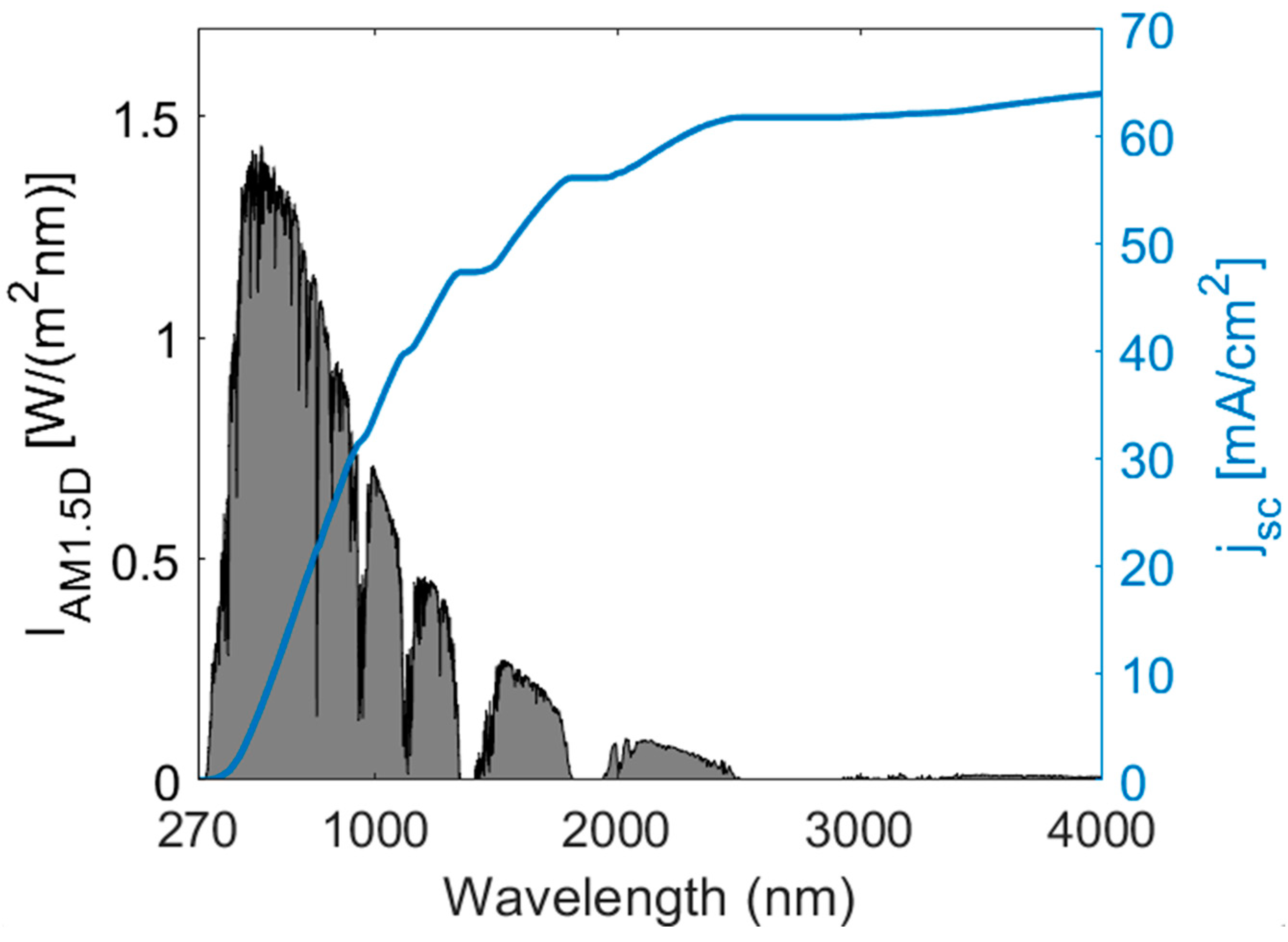
For solar cells, the incident sun-light spectrum on earth spans approximately from 270 to 4000 nm in wavelength [see Figure 2]. With a lower , we can absorb a larger fraction of the incident photons. The short-circuit current can be calculated as where is the elementary charge, is the incident solar spectrum, and is the absorptance, that is, the fraction of incident light that is absorbed (here, it is assumed that each absorbed photon gives rise to one charge carrier to the external current) [16]. See Figure 2 for an example of the maximum obtainable for the case of the IAM1.5D solar spectrum.
Figure 2.
The direct and circumsolar 900 W/m2 IAM1.5D spectrum (grey patched area) is shown with values on the left axis [18]. Here, also the corresponding maximum short-circuit current as a function of bandgap wavelength (blue line) is shown with values on the right axis, under the assumption that all incident above bandgap photons are absorbed, that is, that for .
However, the bandgap energy also limits the voltage at which a solar cell can operate, as detailed by Shockley and Quiesser in 1961 through a detailed balance analysis [19]. Therefore, there is an optimum in the range of ≈1-1.5 eV for optimizing the electrical power output, and hence efficiency, of a solar cell based on a single semiconductor material. The current efficiency record of such a single-junction solar cell is at 29.1%, set by a III-V cell [20], based on GaAs with a bandgap of 1.42 eV (however, due to the high manufacturing cost of GaAs solar cells, the solar cell market is dominated by Si solar cells with record efficiency at 26.8% [20]).
To absorb a larger fraction of the incident photons, without sacrificing output voltage, a multi-junction solar cell approach is useful [13]. In this configuration, the solar cell consists of a stack of sub-cells, with the highest bandgap for the sub-cell at the top and decreasing bandgap down into the stack. In this way, each sub-cell absorbs the photons incident on it at a high efficiency, transmitting lower energy photons to the next sub-cell. With this approach, an efficiency of 47.6% has been reached for a III-V based solar cell, specifically for (GaInP/GaInAs; GaInAsP/GaInAs) 4-junction solar cell under concentrated sunlight [20]. This approach with a multi-junction solar cell has also been investigated for nanowires [21].
For photodetector applications, the incident spectrum is not as fixed as for solar cells. Depending on the application, a photodetector might receive a narrow-band or a broad-band incident spectrum. In this Review, we aim to cover both cases by looking at the overall absorption-tuning in nanowires.
3. Bandgap and refractive index of III-Vs
3.1. Bandgap
We list in Table 1 the bandgap of some of the binary III-Vs common for absorption applications with nanowires. As can be seen, their span a wavelength range from 550 nm to 3500 nm, with a continuous tuning if using their ternary or quaternary compounds. With AlGaP or AlGaAs, we could reach nm [1], but the strong oxidation of Al has somewhat limited this research direction for nanowires. InAsSb is an interesting option for even >10 μm photodetection since the ternary shows at a suitable composition a lower bandgap, with μm, than InAs (3.5 μm) or InSb (7.3 μm) [1,22].

Table 1.
Bandgap, , from Ref. [1] at a temperature of 300 K for selected III-V semiconductors. We show here also the corresponding bandgap wavelength, .
Table 1.
Bandgap, , from Ref. [1] at a temperature of 300 K for selected III-V semiconductors. We show here also the corresponding bandgap wavelength, .
| III-V | Bandgap (eV) | Bandgap wavelength (nm) |
|---|---|---|
| GaP | 2.271 | 546 |
| GaAs | 1.42 | 873 |
| InP | 1.34 | 925 |
| InAs | 0.35 | 3540 |
1GaP shows an indirect bandgap with the direct transitions starting at 2.77 eV [1] , corresponding to 448 nm in photon wavelength.
3.1. Refractive index
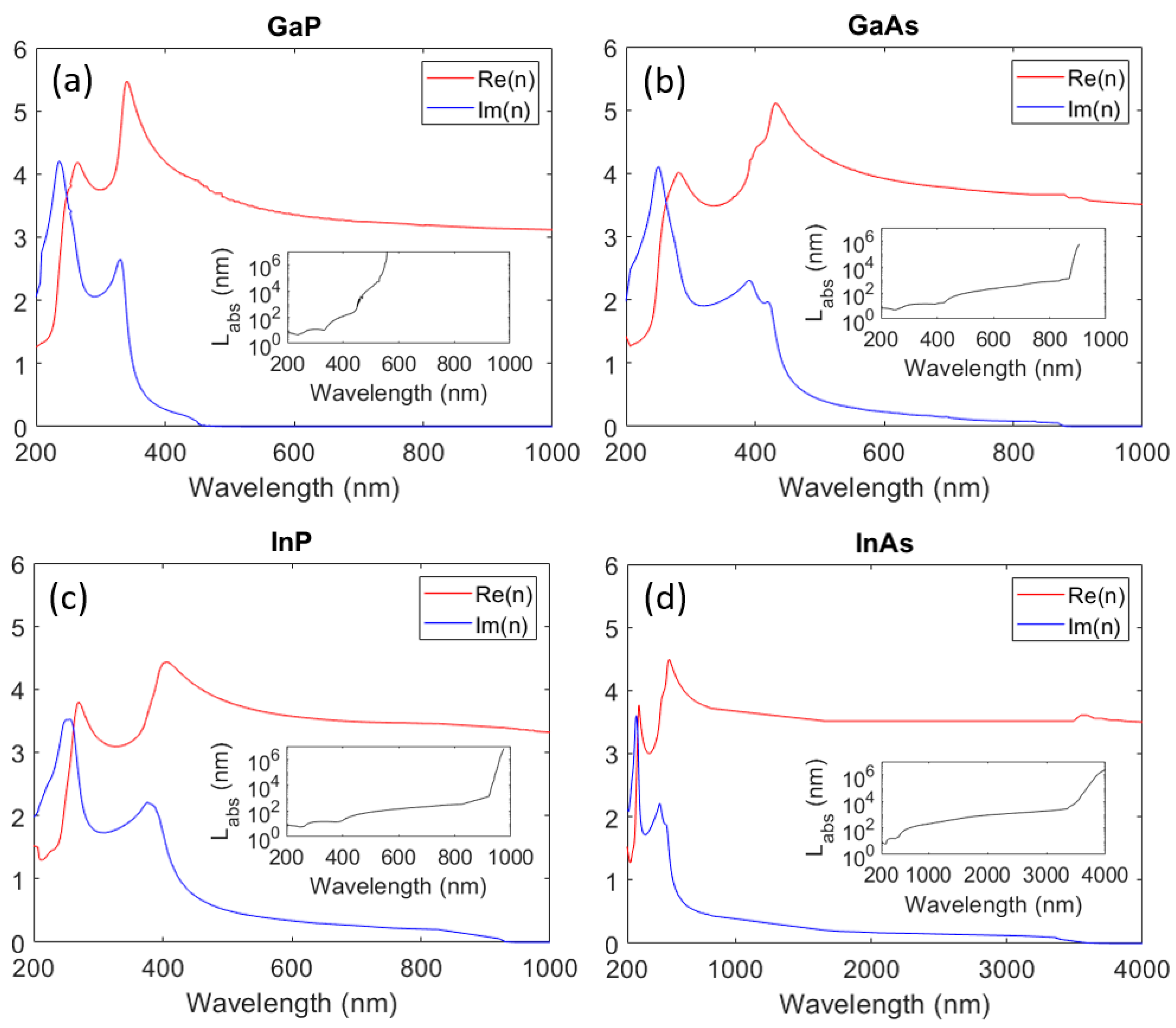
The optical response of materials is described by their wavelength-dependent and complex-valued refractive index . This applies for the linear, local, non-magnetic, and time-harmonic response, and together with the Maxwell equations, it describes theoretically the diffraction of light by structured materials, such as thin films and nanowires [23]. For absorption, , and as an alternative, we can study the absorption length . corresponds to the thickness in bulk semiconductor over which the intensity of propagating light decays to due to absorption.
Out of the III-Vs in Table 1, GaP has an indirect bandgap, which leads to weak absorption from nm to nm where much stronger, direct optical transitions set in. This is seen as a low value for Im(n) for nm, with a rapid increase at nm (Figure 3). For the other III-Vs in Table 1, we find a direct bandgap, and the absorption starts strong directly at , as evident by the relatively high Im(n) values there. There is minor absorption also in the Urbach tail at due to phonon-assisted absorption, but the strength of this absorption drops rapidly with increasing . See Figure 3 for the corresponding for the III-Vs.
For the III-Vs in Table 1, Re(n) is on the order of 3.5 (Figure 3), as compared to 1 for air and 1.5 for typical oxides and polymers. This comparatively high Re(n), and especially its contrast to the surrounding material, gives rise to strong diffraction and potential for resonant absorption in nanowires [24].
For studying the absorption in nanowires, theoretical modelling can be an efficient approach since it allows a fast and cost-efficient way to vary geometrical and material parameters [23]. Specifically, the linear Maxwell equations with the use of is an appealing model since then, the only input is the material choice and geometry for the nanowire system [23]. For nanowire arrays, modelled optical response has been so accurate that we can by comparing modelled and measured spectra extract geometrical parameters such as nanowire diameter and length from fabricated nanowire arrays to an accuracy comparable to that from a scanning electron microscope [25]. Thus, we believe that modelled results are highly accurate for describing the optical response of nanowire arrays.
Figure 3.
Refractive index of the III-V semiconductors GaP, GaAs, InP, and InAs, with tabulated data from Refs. [26,27,28,29], respectively. The insets show the corresponding absorption length on a logarithmic scale. We show here InAs with an extended wavelength range due to its lower bandgap, see Table 1.
4. III-V nanowires
As discussed above, III-Vs show large tuneability in their optical properties. With III-Vs in nanowire form, we (1) have the prospect of more affordable fabrication [5,30,31,32], (2) gain access to materials combinations otherwise limited by lattice mismatch [33,34], and (3) enable fine tuning of optical response due to geometry-induced diffraction effects [24].
Nanowires can be fabricated in two main modes: top-down or bottom-up [35]. Properties (1) and (2) above apply for bottom-up fabricated nanowires while property 3 applies also for top-down fabricated nanowires. In top-down fabrication, a planar bulk sample is selectively etched to leave nanowires. In bottom-up fabrication, nanowires are synthesized directly into the nanowire form, for example through metal-organic vapor-phase epitaxy (MOVPE) or molecular beam epitaxy (MBE). For both top-down and bottom-up fabrication, the nanowire diameter and length, and possible array pattern, can be controlled to a high degree [35].
When the nanowire diameter is large enough, it is motivated to use the bulk value for n(λ) for the nanowire material. For sufficiently small diameter, quantization effects set in, leading to a diameter-dependent shift in the bandgap energy [36]. A rough guide for when quantization effects set in is the exciton Bohr radius [37], which is given in Ref. [37] as 6 nm for GaP, 15 nm for GaAs, 13 nm for InP, and 57 nm in InAs at a temperature of 300 K. In case of quantum-well based nanowire photodetectors [38], due to the quantization in the quantum well, additional considerations for the optical transitions are needed [39]. In the continuation of this Review, we assume for simplicity that the diameter and axial extent of the absorbing III-V regions are large enough, such that quantization effects can be ignored when studying the optical response.
5. Tuning of absorption in vertical III-V nanowires
We focus on the case where the absorption in the nanowires is central, that is, we assume that the nanowires contain the electrically active region from which the separation of photogenerated charge-carriers occur in solar cells and photodetectors.
With a III-V nanowire array transferred to a transparent polymer [40,41], it is possible to directly measure the absorption in the nanowires, for example in an integrating sphere (in contrast to the case of nanowires grown in a native substrate where absorption also in the substrate contributes [42]). Such measurements have shown that nanowires can absorb efficiently the light that would pass between them in a ray-optics description [40,41]. Furthermore, the reflectance was on the order of a few percentage or less, as compared to a typical reflectance on the order of 30% for a planar III-V sample [40,41].
Thus, vertical nanowires can capture light from the surrounding, as also detailed in an early modelling work on Si nanowire arrays [43]. That work focused on small-diameter nanowires. Afterwards, the research field became more and more interested in larger-diameter nanowires where strong diffraction of light can enhance the absorption, for example by 200-fold per volume absorbing material in a III-V nanowire array [24].
Note that Si shows nm, but due to the indirect bandgap of Si, Si is rather weakly absorbing in a broad wavelength range [44]. Therefore, results from absorbing Si nanowire arrays are not necessarily directly transferable to direct bandgap III-V nanowires. However, where suitable, we will give reference to related Si nanowire absorption studies below.
5.1. Basic nanowire array
The basic nanowire array we consider is periodic and defined by the nanowire diameter , nanowire length , and array period [see Figure 1(a) for a schematic]. The absorption is typically not strongly dependent on the type of array, with rather similar absorption found for a square and a hexagonal array, as long as the same nanowire density is used for both arrays [16,45]. In the most basic configuration, the nanowires are on a native substrate of the same material as the nanowires and surrounded by air above and between. In principle, additional processing layers can have noticeable effect on the optical response [16,46], but this basic array functions as a good starting point for more complicated device layouts.
The basic nanowire array has received considerable theoretical interest, and it has been shown that with appropriate geometry choice, the nanowires can absorb incident light very efficiently [2,47,48,49,50,51,52].
5.1.1. Insertion reflection loss
For the above basic nanowire array, a limiting factor for the absorption of light is the insertion reflection loss [2,48]. This reflection occurs at the top of the nanowire array and depends on and , but not on . Typically, this reflection loss decreases with decreasing ratio, especially if considering averaging over a broadband response, such as the above-bandgap part of the solar spectrum that could be absorbed by the semiconductor [2,48].
To couple in as much light as possible into the nanowire array for possible absorption, we would like to decrease the ratio. Indeed, with sparse nanowire arrays, it is possible to reach very good broadband incoupling of light [53]. However, with decreasing ratio, the amount of absorbing semiconductor material in the nanowire array decreases. Therefore, it is not surprising that the optimum ratio for absorption is dependent on . A larger allows for a smaller ratio for optimized absorption of sunlight [2].
5.1.2. Diameter dependent absorption
The diameter of the nanowires has a strong impact on the optical response. When , we are in the geometrical optics regime where light can be described as rays. In this case, for normally incident light, the fraction of light that can be absorbed by the nanowires is limited by the area coverage of the nanowires, that is, the (area) density of nanowires multiplied by the cross-sectional area of a nanowire [24]. At the other extreme, when , we can use an electrostatic description for light. This description reveals a considerably weaker absorption, of normally incident light, in small-diameter nanowires due to electrostatic screening, as compared to a planar semiconductor layer [24] (see Figure 4).
Figure 4.
Modelled absorptance of normally incident light in InP nanowires on InP susbtrate, that is, the same system as studied in Ref. [2], recalculated for this Review in the same way as in Ref. [2] to allow this replotting. (a) L = 2000 nm and P = 680 nm. For this L, P = 680 nm and D = 441 nm gives, a peak of mA/cm2, which occurs when the HE12 absorption peak is placed to the vicinity of the bangdap wavelength. This P and D is the optimum choice if using this HE12 for this L. (b) L = 2000 nm and P = 340 nm. For this L, P = 340 nm and D = 184 nm gives, for any value of D and P, the maximum absorption corresponding to mA/cm2. These values are calculated for the AM1.5D spectrum (see Figure 2) for which the maximum values for InP with eV is 31.1 mA/cm2, which occurs when all above bandgap light is absorbed (see inset in Figure 2). The horizontal scaling in (a) and (b) is set equal to allow easier comparison. Here, to guide the eye, we indicate the absorption peak due to the HE11 and HE12 waveguide modes (dashed lines). The region of low absorptance for small D/λ to the left of the dashed line indicating the HE11 peak originates from the electrostatic screening [24]. For InP, nm, and for , the absorption drops rapidly to negligible values.
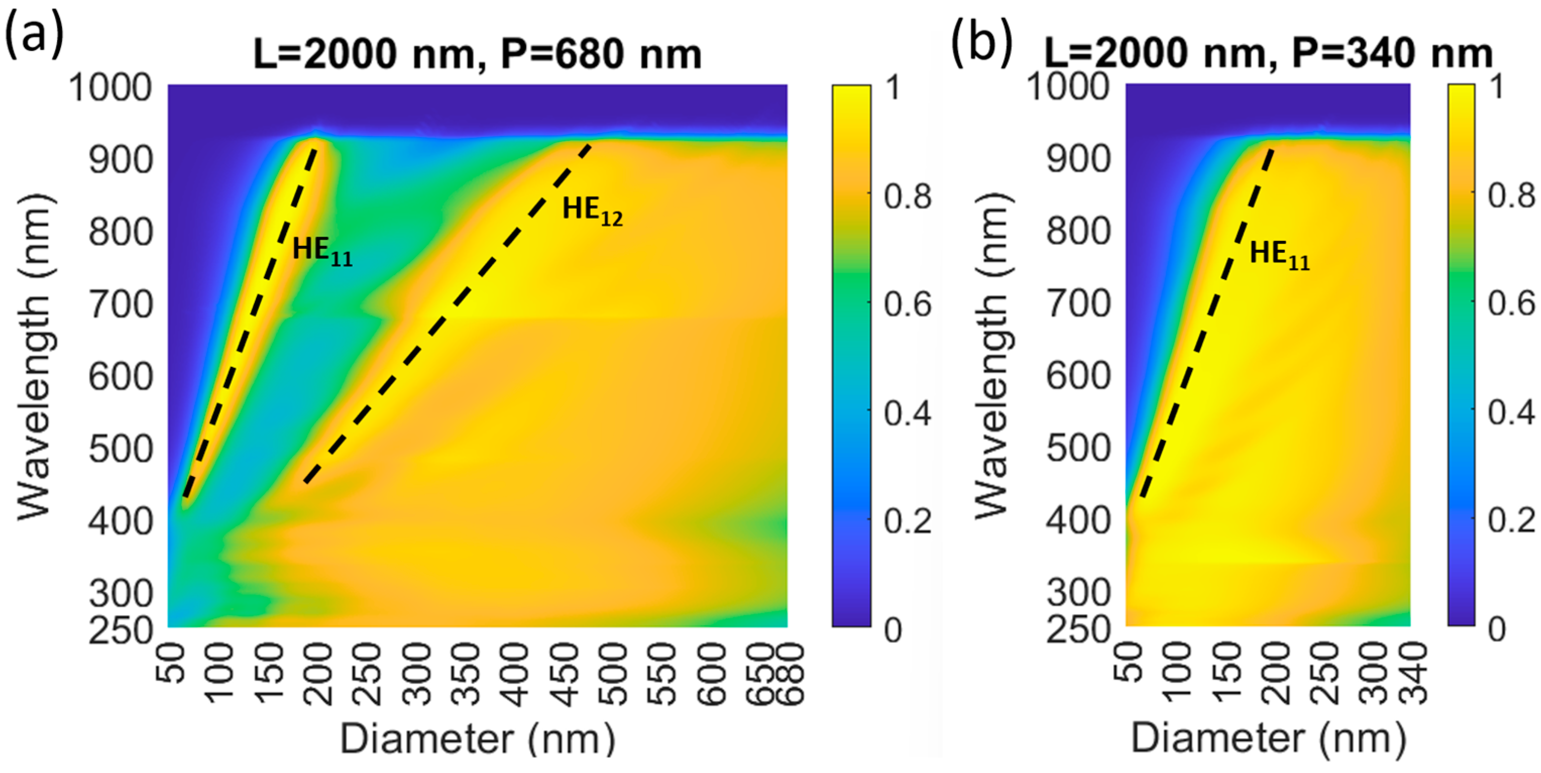
In the intermediate regime where , the nanowires function optically as waveguides, with accompanying electromagnetic waveguide modes [54]. These waveguide modes depend on the nanowire diameter , but not on array period (unless considering a very dense array where nanowire-to-nanowire coupling could affect the dispersion of the waveguide modes [55]).
In our experience, the waveguide modes show up distinctively in the optical response at least when . For shorter nanowires, a description based on elongated Mie scatterers might be more suitable [56].
For normally incident light, we find strongest response from the HE1m modes [2,48,57]. Each HE1m mode gives rise to a distinct absorption peak whose wavelength position can be tuned by the nanowire diameter [2,46,54], as measured initially for the HE11 mode in Si nanowire arrays [58].
The absorption peak due to an HE1m mode originates from two factors. First, with increasing , the waveguide mode becomes more and more bound to the nanowire, which leads to stronger absorption of the light that has coupled into the mode [22,59]. Second, with increasing , since the waveguide mode becomes more and more bound to the nanowire, it has less and less overlap with the incident plane wave and less light couples into the mode [22,59]. Therefore, due to these opposite dependencies on , for an intermediate value for , we find an absorption peak [22,59].
We note that the waveguide-mode dispersion can be scaled with wavelength, taking into account the variation in Re(n) between semiconductors. Thus, it is not surprising that the HE11 mode can be uses to give rise to an absorption peak also for longer wavelength, such as at λ > 3 μm by scaling the diameter to D > 500 nm in InAsSb nanowires [22].
For the broadband absorption of sunlight, it has been found optimal to place the absorption peak due to a HE1m mode in the vicinity of the bandgap wavelength (see Figure 4). In this way, we enhance there the absorption, which is otherwise weak due to the low Im(n) for wavelengths just below the bandgap wavelength. For strongest absorption, it appears that the HE11 mode is the most beneficial to use. Therefore, we find a rather constant optimum for varying nanowire length, while increases with increasing , which in turn decreases the ratio and insertion reflection loss as discussed above. Conveniently, if we have found the optimum for nanowires of one III-V semiconductor, such as in Ref. [2] for InP nanowires, it is possible to estimate the optimum for other III-V semiconductors. Thanks to the scalability of the Maxwell equations, to find the optimum diameter for a different III-V semiconductor, we need to scale with and the bandgap refractive index values: [2]. Here, new and old refer to the two different semiconductor materials and m to the optimization based on HE1m.
An additional avenue to tune to optical response is to use a dielectric shell on top of the nanowire to increase the effective diameter of the nanowire [60]. Such an approach can be effective for example if is too small to reach a desired wavelength with the HE11 absorption peak. This approach does typically however not lead to as strong absorption as when simply increasing the diameter of the absorbing nanowire itself [60].
5.1.4. Photonic-crystal modes in nanowire arrays
The periodic nanowire array has an enumerable set of discrete optical modes [2,46]. In other words, the nanowire array corresponds to a two-dimensional photonic crystal consisting of cylinders [61]. The electromagnetic field, which describes the light inside the nanowire array, can be described fully in terms of these photonic crystal modes. The photonic crystal modes are excited at the top and bottom interface of the nanowire array [2].
Thus, when analyzing theoretically the absorption of light in nanowire arrays, it can be powerful to look at the excitation and absorption of the varying photonic crystal modes present, see for example Appendix C in Ref. [2]. For example in the Fourier modal method (FMM) for solving the Maxwell equations for the scattering of light, that modal information is readily available [23,62].
Compared to conventional photonic crystal research, there are however some noticeable differences. First, we consider nanowires for absorption applications, in which case each photonic crystal mode exhibits some degree of absorption, in contrast to typical photonic crystal research with non-absorbing dielectric materials. Second, we consider excitation by external light, where light at normal angle, that is, parallel to the nanowire axis, corresponds to the Γ point for the photonic crystal. The Γ point for a two-dimensional photonic crystal is typically not of highest interest since due to the continuous translational invariance along the nanowire axis, no photonic bandgap opens up in that direction, since at least one mode is propagating [61] (the HE11 mode is the mode that always stays propagating in the Γ point in the corresponding conventional photonic crystal). Therefore, results from conventional photonic crystal research can have limited applicability for the absorbing nanowire arrays, and dedicated studies about the modal properties in absorbing nanowire arrays are warranted.
5.1.4. Absorption in single nanowire vs nanowire array
The HE1m waveguide modes show up in both single nanowires and nanowire arrays, while the photonic crystal modes are exclusive for the nanowire array. For a single nanowire, a continuum of unbound radiation modes shows up instead [59]. Thus, also single nanowires show the HE1m -based absorption peaks, which are tunable by the nanowire diameter [59]. Therefore, a single nanowire shows optical response strongly set by the HE1m modes. Similarly as for the nanowire array, (1) the excitation of the HE1m mode can be analyzed based on the overlap of the mode with the incident plane-wave, corresponding to the excitation at the tip of the nanowire, and (2) the absorption along the nanowire axis follows from the imaginary part of the propagation constant of the mode [59].
For long enough nanowires, it is possible to see how the radiation modes couple into the nanowire, leading to additional absorption. Thus, this coupling leads to continued absorption, even after the contribution from the much stronger HE1m-absorption has reached a negligible level [59]. Thus, in theory, thanks to incoupling from the radiation modes, a single nanowire shows an unbound absorption cross-section with increasing nanowire length [59]. In contrast, a nanowire in a nanowire array shows a limited absorption cross-section due to competition with neighboring nanowires for absorption of the incident photons [59].
5.1.3. Dependence on the incidence angle
For both solar cells and photodetectors, to maximize the projected area of the device to the incident light, normally incident light is optimum. However, for example in fixed-installed solar cells, due to the shifting sun position in the sky over the day, varying incidence angles occur. It has been shown that strongly absorbing III-V nanowire arrays remain strongly absorbing to large incidence angles of approximately 60° [48,63]. However, when considering a single nanowire in detail, it is seen that the optical response becomes incidence angle dependent—at normal incidence, the response is dominated by the HE1m waveguide modes, but with increasing incidence angle, a Mie-type optical response, which is polarization dependent, is found [64].
5.2. Tapered nanowires
Since the insertion reflection loss in the basic nanowire array decreases with decreasing ratio, it is natural to ask if there is a benefit to use tapered nanowires with increasing diameter further down the nanowire [65]. Indeed, it has been shown that the absorption in such III-V nanocones can surpass the absorption in corresponding untapered nanowires [66,67,68]. The tapered geometry also broadens the -dependent absorption peaks [67,68] by offering a continuum of -values through the length of the nanowire [69], which is of interest for broadband absorption applications, such as solar cells and broadband photodetectors.
5.3. Aperiodic arrays
As discussed above, the HE1m absorption peak is diameter dependent. In order to boost absorption in a broader wavelength range, one approach is to use an aperiodic nanowire array where the diameter varies between the nanowires [70,71], as also proposed for Si nanowires [72,73]. For such aperiodic nanowire arrays, a possible challenge is the formation of the desired pn-junction if fabricated in a bottom-up manner, since the growth and doping conditions might vary nanowire to nanowire.
5.4. Tandem nanowire-on-silicon solar cells
There is prospect of a low-cost nanowire top cell on top of a high-efficiency Si bottom cell to boost the overall efficiency of the solar cell. Since the bandgap of III-Vs can be fine-tuned by the choice of ternary, such as GaInP, it is possible to find a nanowire top-cell material with optimized bandgap to be placed on top of a silicon bottom cell. To enable simultaneous strong absorption of above bandgap photons in the nanowire top cell and efficient transmission of below bandgap photons to the bottom cell, careful optics considerations are needed [74], especially if a lower refractive-index spacer is used between the cells [46]. For efficient design, both optical and electrical modelling is needed [17,75].
5.5. Effect of imperfections in nanowire arrays
In large-area nanowire arrays, varying types of imperfections, including missing nanowires and electrical contacting issues of some nanowires are possible [76]. Characterization of such effects becomes then important [76]. In optics simulations, we have seen that neighboring nanowires can efficiently compensate in absorption for a missing nanowire [77]. Thus, missing nanowires appear as a smaller issue than the lack of electrical contacting of a nanowire [77]. In general, the electrical and optical characterization of individual nanowires in processed nanowire arrays is of interest [78].
5.6. Bragg reflectors in nanowires
III-V nanowires offer novel ways to create periodic refractive variation [79], as needed for example for Bragg reflectors, that is, dielectric reflectors [80]. In nanowires, it is possible to periodically vary the nanowire diameter in the axial direction [81], an avenue not available in conventional thin-film stacks for Bragg reflectors. We envision the use of Bragg reflectors in nanowires for enhanced absorption of sunlight [82] as well as for wavelength selective and enhanced photodetection.
5.7 Examples of realized III-V nanowires solar cells and photodetectors
Research into vertical III-V nanowire solar cells and photodetectors is an active field with multiple studies, e.g. Refs. [22,83,84,85,86,87,88,89,90,91,92,93,94,95,96,97,98,99,100,101]. Below, we comment on some of them and their connection to the absorption of light.
In 2013, a 13.8% efficient bottom-up fabricated InP nanowire array solar cell with 1 mm size and 4 million nanowires was realized [86]. The efficiency relied to a large degree on the optimization of the nanowire diameter and pn-junction configuration to enhance charge extration and [86]. Later, through modelling, it was shown that in such axial pn-junctions, a limiting effect is the extraction of charge carriers from the doped segment closest to the electrical top-side contact [102].
Also in 2013, a solar cell based on a single vertical GaAs nanowire with a short-circuit current density of 180 mA cm–2 was demonstrated [87]. This was obtained by normalizing the short-circuit current in the nanowire to the cross-sectional area of the nanowire, and it is approximately 6 times higher than the maximum value in a conventional GaAs bulk solar cell [20]. Thus, that study clearly shows the excellent possibility for nanowires to capture light from their surroundings.
In 2016, a 15.3% efficient bottom-up fabricated GaAs nanowire array solar cell was reported [93]. For this study, a nanoprobe-contacting scheme inside a scanning electron microscope was used. This electrical contacting allowed electron beam induced current-measurements, which reveal the spatial variation of charge carrier collection. Also in 2016, with such a nanoprobe contacting and characterization for the development, a 15.0% efficient bottom-up fabricated InP nanowire array solar cell was reported [96].
In 2016, a 17.8% efficient top-down fabricated InP nanowire array was shown [94], which currently stands as the record efficiency for III-V nanowire array solar cells. In the initial planar growth, excellent control over the profile for the pn-junction is achieved, leading to high open-circuit voltage and fill-factor. In that study, indium-tin-oxide particles functioned as Mie scatterers to enhance the absorption of light in the top-down etched nanowires.
In 2019, an InP nanowire array photodetector for single photon detection with peak efficiency above 90%, without the need of cryogenic cooling, was demonstrated [98]. The excellent optical performance was partly thanks to a tapered design of the nanowires. Two years later, in 2021, a self-powered InP nanowire array photodetector for single photon detection at room temperature was demonstrated [99].
6. Future directions
Below, we list some future directions that we find of particular interest for solar cells and photodetectors where nanowires could benefit from their unique properties.
For nanowire solar cells, an ongoing and future direction is the epitaxial fabrication of a multi-junction cell into the nanowires themselves, as already demonstrated with GaInP/InP/InAsP triple-junction photovoltaic nanowires [21]. This approach benefits from the freedom in combining materials in the nanowire, despite lattice mismatch. Furthermore, nanowires have been shown to be radiation hard [103], giving the prospect of light-weight and efficient multi-junction nanowire solar cells for space applications. We note that for efficient absorption in the varying segments of such nanowires, some additional geometry design considerations arise compared to the single-junction case [104].
An another venue with the nanowires is enabled by embedding them into a flexible host, such as a polymer matrix [40,41]. This gives the prospect for mass-production of flexible solar cells, if the nanowires can be successfully contacted electrically and fabricated at a low enough cost. We envision here a flexible high-efficiency multi-junction nanowire solar cell for wearables.
Bulk non-nitride III-Vs show up in the zinc-blende crystal phase. Nanowires give however the option to synthesize also the wurtzite crystal phase [105]. The refractive index varies between these two phases to such a degree that it affects into which wavelength ranges the HE1m absorption peaks can be tuned with the geometry-choice for nanowires [106,107,108]. An interesting future venue could be to explore the possibilities for finte-tuning the absorption of light, as enabled by mixing these two phases in varying axial segments in nanowires.
Above, we have implicitly assumed thermalized carriers in the nanowires. However, in the photogeneration process, hot electrons and hot holes are created in the nanowires due to the excess energy of the absorbed, incident photon. An interesting ongoing and future avenue is the use of hot-carrier effects in nanowire-based solar cells and photodetectors [109]. There, the unique tailoring of the optical and electrical response in nanowires could bring forth benefits beyond planar hot-carrier systems [109].
Funding
This research received no external funding.
Data Availability Statement
No new data were created or analyzed in this study. Data sharing is not applicable to this article.
Conflicts of Interest
The authors declare no conflict of interest.
References
- Vurgaftman, I.; Meyer, J.R.; Ram-Mohan, L.R. Band Parameters for III–V Compound Semiconductors and Their Alloys. J. Appl. Phys. 2001, 89, 5815–5875. [Google Scholar] [CrossRef]
- Anttu, N.; Xu, H.Q. Efficient Light Management in Vertical Nanowire Arrays for Photovoltaics. Opt. Express 2013, 21, A558–A575. [Google Scholar] [CrossRef] [PubMed]
- Li, Z.; Tan, H.H.; Jagadish, C.; Fu, L. III–V Semiconductor Single Nanowire Solar Cells: A Review. Adv. Mater. Technol. 2018, 3, 1800005. [Google Scholar] [CrossRef]
- VJ, L.; Oh, J.; Nayak, A.P.; Katzenmeyer, A.M.; Gilchrist, K.H.; Grego, S.; Kobayashi, N.P.; Wang, S.-Y.; Talin, A.A.; Dhar, N.K.; et al. A Perspective on Nanowire Photodetectors: Current Status, Future Challenges, and Opportunities. IEEE J. Sel. Top. Quantum Electron. 2011, 17, 1002–1032. [Google Scholar] [CrossRef]
- Otnes, G.; Borgström, M.T. Towards High Efficiency Nanowire Solar Cells. Nano Today 2017, 12, 31–45. [Google Scholar] [CrossRef]
- LaPierre, R.R.; Robson, M.; Azizur-Rahman, K.M.; Kuyanov, P. A Review of III–V Nanowire Infrared Photodetectors and Sensors. J. Phys. Appl. Phys. 2017, 50, 123001. [Google Scholar] [CrossRef]
- LaPierre, R.R.; Chia, A.C.E.; Gibson, S.J.; Haapamaki, C.M.; Boulanger, J.; Yee, R.; Kuyanov, P.; Zhang, J.; Tajik, N.; Jewell, N.; et al. III–V Nanowire Photovoltaics: Review of Design for High Efficiency. Phys. Status Solidi RRL – Rapid Res. Lett. 2013, 7, 815–830. [Google Scholar] [CrossRef]
- Nanowires for Energy: A Review | Applied Physics Reviews | AIP Publishing. Available online: https://pubs.aip.org/aip/apr/article-abstract/5/4/041305/124236/Nanowires-for-energy-A-review?redirectedFrom=fulltext (accessed on 11 July 2023).
- Mukai, T. Recent Progress in Group-III Nitride Light-Emitting Diodes. IEEE J. Sel. Top. Quantum Electron. 2002, 8, 264–270. [Google Scholar] [CrossRef]
- REN21. 2022. Renewables 2022 Global Status Report. (Paris: REN21 Secretariat). ISBN 978-3-948393-04-5.
- Downs, C.; Vandervelde, T.E. Progress in Infrared Photodetectors Since 2000. Sensors 2013, 13, 5054–5098. [Google Scholar] [CrossRef] [PubMed]
- Sze, S.M.; Li, Y.; Ng, K.K. Physics of Semiconductor Devices; John Wiley & Sons, 2021; ISBN 978-1-119-61800-3. [Google Scholar]
- Nelson, J. PHYSICS OF SOLAR CELLS, THE; 1st edition.; ICP: London: River Edge, NJ, 2003; ISBN 978-1-86094-349-2. [Google Scholar]
- Alhalaili, B.; Peksu, E.; Mcphillips, L.N.; Ombaba, M.M.; Islam, M.S.; Karaagac, H. 4 - Nanowires for Photodetection. In Photodetectors (Second Edition); Woodhead Publishing Series in Electronic and Optical Materials; Nabet, B., Ed.; Woodhead Publishing, 2023; pp. 139–197. ISBN 978-0-08-102795-0. [Google Scholar]
- Trojnar, A.H.; Valdivia, C.E.; LaPierre, R.R.; Hinzer, K.; Krich, J.J. Optimizations of GaAs Nanowire Solar Cells. IEEE J. Photovolt. 2016, 6, 1494–1501. [Google Scholar] [CrossRef]
- Anttu, N. Physics and Design for 20% and 25% Efficiency Nanowire Array Solar Cells. Nanotechnology 2018, 30, 074002. [Google Scholar] [CrossRef] [PubMed]
- Maryasin, V.; Bucci, D.; Rafhay, Q.; Panicco, F.; Michallon, J.; Kaminski-Cachopo, A. Technological Guidelines for the Design of Tandem III-V Nanowire on Si Solar Cells from Opto-Electrical Simulations. Sol. Energy Mater. Sol. Cells 2017, 172, 314–323. [Google Scholar] [CrossRef]
- ASTM G173-03(2020), Standard Tables for Reference Solar Spectral Irradiances: Direct Normal and Hemispherical on 37° Tilted Surface, ASTM International, West Conshohocken, PA, 2020.
- Shockley, W.; Queisser, H.J. Detailed Balance Limit of Efficiency of P-n Junction Solar Cells. J. Appl. Phys. 1961, 32, 510–519. [Google Scholar] [CrossRef]
- Green, M.A.; Dunlop, E.D.; Yoshita, M.; Kopidakis, N.; Bothe, K.; Siefer, G.; Hao, X. Solar Cell Efficiency Tables (Version 62). Prog. Photovolt. Res. Appl. 2023, 31, 651–663. [Google Scholar] [CrossRef]
- Hrachowina, L.; Chen, Y.; Barrigón, E.; Wallenberg, R.; Borgström, M.T. Realization of Axially Defined GaInP/InP/InAsP Triple-Junction Photovoltaic Nanowires for High-Performance Solar Cells. Mater. Today Energy 2022, 27, 101050. [Google Scholar] [CrossRef]
- Svensson, J.; Anttu, N.; Vainorius, N.; Borg, B.M.; Wernersson, L.-E. Diameter-Dependent Photocurrent in InAsSb Nanowire Infrared Photodetectors. Nano Lett. 2013, 13, 1380–1385. [Google Scholar] [CrossRef] [PubMed]
- Anttu, N.; Mäntynen, H.; Sorokina, A.; Turunen, J.; Sadi, T.; Lipsanen, H. Applied Electromagnetic Optics Simulations for Nanophotonics. J. Appl. Phys. 2021, 129, 131102. [Google Scholar] [CrossRef]
- Anttu, N. Geometrical Optics, Electrostatics, and Nanophotonic Resonances in Absorbing Nanowire Arrays. Opt. Lett. 2013, 38, 730–732. [Google Scholar] [CrossRef]
- Anttu, N.; Heurlin, M.; Borgström, M.T.; Pistol, M.-E.; Xu, H.Q.; Samuelson, L. Optical Far-Field Method with Subwavelength Accuracy for the Determination of Nanostructure Dimensions in Large-Area Samples. Nano Lett. 2013, 13, 2662–2667. [Google Scholar] [CrossRef] [PubMed]
- Borghesi, A.; Guizzetti, G. Gallium Phosphide (GaP). In Handbook of Optical Constants of Solids; Palik, E.D., Ed.; Academic Press: Boston, 1985; pp. 445–464. ISBN 978-0-08-054721-3. [Google Scholar]
- Palik, E.D. Gallium Arsenide (GaAs). In Handbook of Optical Constants of Solids; Palik, E.D., Ed.; Academic Press: Boston, 1985; pp. 429–443. ISBN 978-0-08-054721-3. [Google Scholar]
- Glembocki, O.J.; Piller, H. Indium Phosphide (InP). In Handbook of Optical Constants of Solids; Palik, E.D., Ed.; Academic Press: Burlington, 1997; pp. 503–516. ISBN 978-0-12-544415-6. [Google Scholar]
- Pauk, E.D.; Holm, R.T. Indium Arsenide (InAs). In Handbook of Optical Constants of Solids; Palik, E.D., Ed.; Academic Press: Burlington, 1997; pp. 479–489. ISBN 978-0-12-544415-6. [Google Scholar]
- Raj, V.; Haggren, T.; Wong, W.W.; Tan, H.H.; Jagadish, C. Topical Review: Pathways toward Cost-Effective Single-Junction III–V Solar Cells. J. Phys. Appl. Phys. 2021, 55, 143002. [Google Scholar] [CrossRef]
- Zhang, Y.; Liu, H. Nanowires for High-Efficiency, Low-Cost Solar Photovoltaics. Crystals 2019, 9, 87. [Google Scholar] [CrossRef]
- Barrigón, E.; Hultin, O.; Lindgren, D.; Yadegari, F.; Magnusson, M.H.; Samuelson, L.; Johansson, L.I.M.; Björk, M.T. GaAs Nanowire Pn-Junctions Produced by Low-Cost and High-Throughput Aerotaxy. Nano Lett. 2018, 18, 1088–1092. [Google Scholar] [CrossRef] [PubMed]
- Chuang, L.C.; Moewe, M.; Chase, C.; Kobayashi, N.P.; Chang-Hasnain, C.; Crankshaw, S. Critical Diameter for III-V Nanowires Grown on Lattice-Mismatched Substrates. Appl. Phys. Lett. 2007, 90, 043115. [Google Scholar] [CrossRef]
- Caroff, P.; Messing, M.E.; Borg, B.M.; Dick, K.A.; Deppert, K.; Wernersson, L.-E. InSb Heterostructure Nanowires: MOVPE Growth under Extreme Lattice Mismatch. Nanotechnology 2009, 20, 495606. [Google Scholar] [CrossRef]
- Barrigón, E.; Heurlin, M.; Bi, Z.; Monemar, B.; Samuelson, L. Synthesis and Applications of III–V Nanowires. Chem. Rev. 2019, 119, 9170–9220. [Google Scholar] [CrossRef] [PubMed]
- Loitsch, B.; Rudolph, D.; Morkötter, S.; Döblinger, M.; Grimaldi, G.; Hanschke, L.; Matich, S.; Parzinger, E.; Wurstbauer, U.; Abstreiter, G.; et al. Tunable Quantum Confinement in Ultrathin, Optically Active Semiconductor Nanowires Via Reverse-Reaction Growth. Adv. Mater. 2015, 27, 2195–2202. [Google Scholar] [CrossRef]
- Shokhovets, S.; Gobsch, G.; Ambacher, O. Excitonic Contribution to the Optical Absorption in Zinc-Blende III-V Semiconductors. Phys. Rev. B 2006, 74, 155209. [Google Scholar] [CrossRef]
- Erhard, N.; Zenger, S.; Morkötter, S.; Rudolph, D.; Weiss, M.; Krenner, H.J.; Karl, H.; Abstreiter, G.; Finley, J.J.; Koblmüller, G.; et al. Ultrafast Photodetection in the Quantum Wells of Single AlGaAs/GaAs-Based Nanowires. Nano Lett. 2015, 15, 6869–6874. [Google Scholar] [CrossRef]
- Warburton, R.J.; Gauer, C.; Wixforth, A.; Kotthaus, J.P.; Brar, B.; Kroemer, H. Intersubband Resonances in InAs/AlSb Quantum Wells: Selection Rules, Matrix Elements, and the Depolarization Field. Phys. Rev. B 1996, 53, 7903–7910. [Google Scholar] [CrossRef]
- Anttu, N.; Abrand, A.; Asoli, D.; Heurlin, M.; Åberg, I.; Samuelson, L.; Borgström, M. Absorption of Light in InP Nanowire Arrays. Nano Res. 2014, 7, 816–823. [Google Scholar] [CrossRef]
- Hu, S.; Chi, C.-Y.; T. Fountaine, K.; Yao, M.; A. Atwater, H.; Daniel Dapkus, P.; S. Lewis, N.; Zhou, C. Optical, Electrical, and Solar Energy-Conversion Properties of Gallium Arsenide Nanowire -Array Photoanodes. Energy Environ. Sci. 2013, 6, 1879–1890. [Google Scholar] [CrossRef]
- Anttu, N.; Iqbal, A.; Heurlin, M.; Samuelson, L.; Borgström, M.T.; Pistol, M.-E.; Yartsev, A. Reflection Measurements to Reveal the Absorption in Nanowire Arrays. Opt. Lett. 2013, 38, 1449–1451. [Google Scholar] [CrossRef] [PubMed]
- Hu, L.; Chen, G. Analysis of Optical Absorption in Silicon Nanowire Arrays for Photovoltaic Applications. Nano Lett. 2007, 7, 3249–3252. [Google Scholar] [CrossRef]
- Green, M.A. Self-Consistent Optical Parameters of Intrinsic Silicon at 300K Including Temperature Coefficients. Sol. Energy Mater. Sol. Cells 2008, 92, 1305–1310. [Google Scholar] [CrossRef]
- Mariani, G.; Zhou, Z.; Scofield, A.; Huffaker, D.L. Direct-Bandgap Epitaxial Core–Multishell Nanopillar Photovoltaics Featuring Subwavelength Optical Concentrators. Nano Lett. 2013, 13, 1632–1637. [Google Scholar] [CrossRef]
- Dagytė, V.; Anttu, N. Modal Analysis of Resonant and Non-Resonant Optical Response in Semiconductor Nanowire Arrays. Nanotechnology 2018, 30, 025710. [Google Scholar] [CrossRef] [PubMed]
- Kupec, J.; Witzigmann, B. Dispersion, Wave Propagation and Efficiency Analysis of Nanowire Solar Cells. Opt. Express 2009, 17, 10399–10410. [Google Scholar] [CrossRef] [PubMed]
- Anttu, N.; Xu, H.Q. Coupling of Light into Nanowire Arrays and Subsequent Absorption. J. Nanosci. Nanotechnol. 2010, 10, 7183–7187. [Google Scholar] [CrossRef] [PubMed]
- Guo, H.; Wen, L.; Li, X.; Zhao, Z.; Wang, Y. Analysis of Optical Absorption in GaAs Nanowire Arrays. Nanoscale Res. Lett. 2011, 6, 617. [Google Scholar] [CrossRef] [PubMed]
- Wen, L.; Zhao, Z.; Li, X.; Shen, Y.; Guo, H.; Wang, Y. Theoretical Analysis and Modeling of Light Trapping in High Efficicency GaAs Nanowire Array Solar Cells. Appl. Phys. Lett. 2011, 99, 143116. [Google Scholar] [CrossRef]
- Hu, Y.; LaPierre, R.R.; Li, M.; Chen, K.; He, J.-J. Optical Characteristics of GaAs Nanowire Solar Cells. J. Appl. Phys. 2012, 112, 104311. [Google Scholar] [CrossRef]
- Huang, N.; Lin, C.; Povinelli, M.L. Broadband Absorption of Semiconductor Nanowire Arrays for Photovoltaic Applications. J. Opt. 2012, 14, 024004. [Google Scholar] [CrossRef]
- Fountaine, K.T.; Cheng, W.-H.; Bukowsky, C.R.; Atwater, H.A. Near-Unity Unselective Absorption in Sparse InP Nanowire Arrays. ACS Photonics 2016, 3, 1826–1832. [Google Scholar] [CrossRef]
- Snyder, A.W.; Love, J.D. Optical Waveguide Theory; Springer US: Boston, MA, 1984; ISBN 978-0-412-24250-2. [Google Scholar]
- Mäntynen, H.; Anttu, N.; Lipsanen, H. Nanowire Oligomer Waveguide Modes towards Reduced Lasing Threshold. Materials 2020, 13, 5510. [Google Scholar] [CrossRef] [PubMed]
- Traviss, D.J.; Schmidt, M.K.; Aizpurua, J.; Muskens, O.L. Antenna Resonances in Low Aspect Ratio Semiconductor Nanowires. Opt. Express 2015, 23, 22771–22787. [Google Scholar] [CrossRef]
- Wang, B.; Leu, P.W. Tunable and Selective Resonant Absorption in Vertical Nanowires. Opt. Lett. 2012, 37, 3756–3758. [Google Scholar] [CrossRef] [PubMed]
- Seo, K.; Wober, M.; Steinvurzel, P.; Schonbrun, E.; Dan, Y.; Ellenbogen, T.; Crozier, K.B. Multicolored Vertical Silicon Nanowires. Nano Lett. 2011, 11, 1851–1856. [Google Scholar] [CrossRef]
- Anttu, N. Absorption of Light in a Single Vertical Nanowire and a Nanowire Array. Nanotechnology 2019, 30, 104004. [Google Scholar] [CrossRef] [PubMed]
- Anttu, N.; Namazi, K.L.; Wu, P.M.; Yang, P.; Xu, H.; Xu, H.Q.; Håkanson, U. Drastically Increased Absorption in Vertical Semiconductor Nanowire Arrays: A Non-Absorbing Dielectric Shell Makes the Difference. Nano Res. 2012, 5, 863–874. [Google Scholar] [CrossRef]
- Photonic Crystals: Molding the Flow of Light. Available online: http://ab-initio.mit.edu/book/ (accessed on 16 June 2020).
- Anttu, N.; Mäntynen, H.; Sadi, T.; Matikainen, A.; Turunen, J.; Lipsanen, H. Comparison of Absorption Simulation in Semiconductor Nanowire and Nanocone Arrays with the Fourier Modal Method, the Finite Element Method, and the Finite-Difference Time-Domain Method. Nano Express 2020, 1, 030034. [Google Scholar] [CrossRef]
- Ghahfarokhi, O.M.; Anttu, N.; Samuelson, L.; Åberg, I. Performance of GaAs Nanowire Array Solar Cells for Varying Incidence Angles. IEEE J. Photovolt. 2016, 6, 1502–1508. [Google Scholar] [CrossRef]
- Abujetas, D.R.; Paniagua-Domínguez, R.; Sánchez-Gil, J.A. Unraveling the Janus Role of Mie Resonances and Leaky/Guided Modes in Semiconductor Nanowire Absorption for Enhanced Light Harvesting. ACS Photonics 2015, 2, 921–929. [Google Scholar] [CrossRef]
- Fan, Z.; Kapadia, R.; Leu, P.W.; Zhang, X.; Chueh, Y.-L.; Takei, K.; Yu, K.; Jamshidi, A.; Rathore, A.A.; Ruebusch, D.J.; et al. Ordered Arrays of Dual-Diameter Nanopillars for Maximized Optical Absorption. Nano Lett. 2010, 10, 3823–3827. [Google Scholar] [CrossRef]
- Diedenhofen, S.L.; Janssen, O.T.A.; Grzela, G.; Bakkers, E.P.A.M.; Gómez Rivas, J. Strong Geometrical Dependence of the Absorption of Light in Arrays of Semiconductor Nanowires. ACS Nano 2011, 5, 2316–2323. [Google Scholar] [CrossRef] [PubMed]
- Wang, B.; Stevens, E.; Leu, P.W. Strong Broadband Absorption in GaAs Nanocone and Nanowire Arrays for Solar Cells. Opt. Express 2014, 22, A386–A395. [Google Scholar] [CrossRef] [PubMed]
- Wilson, D.P.; LaPierre, R.R. Simulation of Optical Absorption in Conical Nanowires. Opt. Express 2021, 29, 9544–9552. [Google Scholar] [CrossRef] [PubMed]
- Tekcan, B.; van Kasteren, B.; Grayli, S.V.; Shen, D.; Tam, M.C.; Ban, D.; Wasilewski, Z.; Tsen, A.W.; Reimer, M.E. Semiconductor Nanowire Metamaterial for Broadband Near-Unity Absorption. Sci. Rep. 2022, 12, 9663. [Google Scholar] [CrossRef]
- Wu, D.; Tang, X.; Wang, K.; Li, X. An Analytic Approach for Optimal Geometrical Design of GaAs Nanowires for Maximal Light Harvesting in Photovoltaic Cells. Sci. Rep. 2017, 7, 46504. [Google Scholar] [CrossRef] [PubMed]
- Yan, X.; Gong, L.; Ai, L.; Wei, W.; Zhang, X.; Ren, X. Enhanced Photovoltaic Performance of Nanowire Array Solar Cells with Multiple Diameters. Opt. Express 2018, 26, A974–A983. [Google Scholar] [CrossRef] [PubMed]
- Lin, C.; Povinelli, M.L. Optimal Design of Aperiodic, Vertical Silicon Nanowire Structures for Photovoltaics. Opt. Express 2011, 19, A1148–A1154. [Google Scholar] [CrossRef] [PubMed]
- Sturmberg, B.C.P.; Dossou, K.B.; Botten, L.C.; Asatryan, A.A.; Poulton, C.G.; McPhedran, R.C.; Sterke, C.M. de Absorption Enhancing Proximity Effects in Aperiodic Nanowire Arrays. Opt. Express 2013, 21, A964–A969. [Google Scholar] [CrossRef]
- Chen, Y.; Höhn, O.; Tucher, N.; Pistol, M.-E.; Anttu, N. Optical Analysis of a III-V-Nanowire-Array-on-Si Dual Junction Solar Cell. Opt. Express 2017, 25, A665–A679. [Google Scholar] [CrossRef] [PubMed]
- Benali, A.; Michallon, J.; Regreny, P.; Drouard, E.; Rojo, P.; Chauvin, N.; Bucci, D.; Fave, A.; Kaminski-Cachopo, A.; Gendry, M. Optical Simulation of Multijunction Solar Cells Based on III-V Nanowires on Silicon. Energy Procedia 2014, 60, 109–115. [Google Scholar] [CrossRef]
- Alcer, D.; Hrachowina, L.; Hessman, D.; Borgström, M.T. Processing and Characterization of Large Area InP Nanowire Photovoltaic Devices. Nanotechnology 2023, 34, 295402. [Google Scholar] [CrossRef]
- Anttu, N. Absorption of Light in Finite Semiconductor Nanowire Arrays and the Effect of Missing Nanowires. Symmetry 2021, 13, 1654. [Google Scholar] [CrossRef]
- Li, Z.; Li, L.; Wang, F.; Xu, L.; Gao, Q.; Alabadla, A.; Peng, K.; Vora, K.; T. Hattori, H.; Hoe Tan, H.; et al. Investigation of Light–Matter Interaction in Single Vertical Nanowires in Ordered Nanowire Arrays. Nanoscale 2022, 14, 3527–3536. [Google Scholar] [CrossRef] [PubMed]
- Grain, N.; Kim, S. Insight into Refractive Index Modulation as Route to Enhanced Light Coupling in Semiconductor Nanowires. Opt. Lett. 2023, 48, 227–230. [Google Scholar] [CrossRef] [PubMed]
- A, S.B.E. Fundamentals of Photonics, 2nd Ed.; W, 2012.
- Wilson, D.P.; LaPierre, R.R. Corrugated Nanowires as Distributed Bragg Reflectors. Nano Express 2022, 3, 035005. [Google Scholar] [CrossRef]
- Aghaeipour, M.; Pettersson, H. Enhanced Broadband Absorption in Nanowire Arrays with Integrated Bragg Reflectors. Nanophotonics 2018, 7, 819–825. [Google Scholar] [CrossRef]
- Czaban, J.A.; Thompson, D.A.; LaPierre, R.R. GaAs Core−Shell Nanowires for Photovoltaic Applications. Nano Lett. 2009, 9, 148–154. [Google Scholar] [CrossRef] [PubMed]
- Colombo, C.; Heiβ, M.; Grätzel, M.; Fontcuberta i Morral, A. Gallium Arsenide P-i-n Radial Structures for Photovoltaic Applications. Appl. Phys. Lett. 2009, 94, 173108. [Google Scholar] [CrossRef]
- Goto, H.; Nosaki, K.; Tomioka, K.; Hara, S.; Hiruma, K.; Motohisa, J.; Fukui, T. Growth of Core–Shell InP Nanowires for Photovoltaic Application by Selective-Area Metal Organic Vapor Phase Epitaxy. Appl. Phys. Express 2009, 2, 035004. [Google Scholar] [CrossRef]
- Wallentin, J.; Anttu, N.; Asoli, D.; Huffman, M.; Åberg, I.; Magnusson, M.H.; Siefer, G.; Fuss-Kailuweit, P.; Dimroth, F.; Witzigmann, B.; et al. InP Nanowire Array Solar Cells Achieving 13.8% Efficiency by Exceeding the Ray Optics Limit. Science 2013, 339, 1057–1060. [Google Scholar] [CrossRef]
- Krogstrup, P.; Jørgensen, H.I.; Heiss, M.; Demichel, O.; Holm, J.V.; Aagesen, M.; Nygard, J.; Fontcuberta i Morral, A. Single-Nanowire Solar Cells beyond the Shockley–Queisser Limit. Nat. Photonics 2013, 7, 306–310. [Google Scholar] [CrossRef]
- Mariani, G.; Scofield, A.C.; Hung, C.-H.; Huffaker, D.L. GaAs Nanopillar-Array Solar Cells Employing in Situ Surface Passivation. Nat. Commun. 2013, 4, 1497. [Google Scholar] [CrossRef] [PubMed]
- Yao, M.; Huang, N.; Cong, S.; Chi, C.-Y.; Seyedi, M.A.; Lin, Y.-T.; Cao, Y.; Povinelli, M.L.; Dapkus, P.D.; Zhou, C. GaAs Nanowire Array Solar Cells with Axial p–i–n Junctions. Nano Lett. 2014, 14, 3293–3303. [Google Scholar] [CrossRef]
- Cui, Y.; Wang, J.; Plissard, S.R.; Cavalli, A.; Vu, T.T.T.; van Veldhoven, R.P.J.; Gao, L.; Trainor, M.; Verheijen, M.A.; Haverkort, J.E.M.; et al. Efficiency Enhancement of InP Nanowire Solar Cells by Surface Cleaning. Nano Lett. 2013, 13, 4113–4117. [Google Scholar] [CrossRef] [PubMed]
- Yao, M.; Cong, S.; Arab, S.; Huang, N.; Povinelli, M.L.; Cronin, S.B.; Dapkus, P.D.; Zhou, C. Tandem Solar Cells Using GaAs Nanowires on Si: Design, Fabrication, and Observation of Voltage Addition. Nano Lett. 2015, 15, 7217–7224. [Google Scholar] [CrossRef] [PubMed]
- Ko, W.S.; Tran, T.-T.D.; Bhattacharya, I.; Ng, K.W.; Sun, H.; Chang-Hasnain, C. Illumination Angle Insensitive Single Indium Phosphide Tapered Nanopillar Solar Cell. Nano Lett. 2015, 15, 4961–4967. [Google Scholar] [CrossRef] [PubMed]
- Åberg, I.; Vescovi, G.; Asoli, D.; Naseem, U.; Gilboy, J.P.; Sundvall, C.; Dahlgren, A.; Svensson, K.E.; Anttu, N.; Björk, M.T.; et al. A GaAs Nanowire Array Solar Cell With 15.3% Efficiency at 1 Sun. IEEE J. Photovolt. 2016, 6, 185–190. [Google Scholar] [CrossRef]
- van Dam, D.; van Hoof, N.J.J.; Cui, Y.; van Veldhoven, P.J.; Bakkers, E.P.A.M.; Gómez Rivas, J.; Haverkort, J.E.M. High-Efficiency Nanowire Solar Cells with Omnidirectionally Enhanced Absorption Due to Self-Aligned Indium–Tin–Oxide Mie Scatterers. ACS Nano 2016, 10, 11414–11419. [Google Scholar] [CrossRef] [PubMed]
- Sanatinia, R.; Berrier, A.; Dhaka, V.; Perros, A.P.; Huhtio, T.; Lipsanen, H.; Anand, S. Wafer-Scale Self-Organized InP Nanopillars with Controlled Orientation for Photovoltaic Devices. Nanotechnology 2015, 26, 415304. [Google Scholar] [CrossRef] [PubMed]
- Otnes, G.; Barrigón, E.; Sundvall, C.; Svensson, K.E.; Heurlin, M.; Siefer, G.; Samuelson, L.; Åberg, I.; Borgström, M.T. Understanding InP Nanowire Array Solar Cell Performance by Nanoprobe-Enabled Single Nanowire Measurements. Nano Lett. 2018, 18, 3038–3046. [Google Scholar] [CrossRef]
- Mukherjee, A.; Ren, D.; Vullum, P.-E.; Huh, J.; Fimland, B.-O.; Weman, H. GaAs/AlGaAs Nanowire Array Solar Cell Grown on Si with Ultrahigh Power-per-Weight Ratio. ACS Photonics 2021, 8, 2355–2366. [Google Scholar] [CrossRef]
- Gibson, S.J.; van Kasteren, B.; Tekcan, B.; Cui, Y.; van Dam, D.; Haverkort, J.E.M.; Bakkers, E.P.A.M.; Reimer, M.E. Tapered InP Nanowire Arrays for Efficient Broadband High-Speed Single-Photon Detection. Nat. Nanotechnol. 2019, 14, 473–479. [Google Scholar] [CrossRef] [PubMed]
- Zhu, Y.; Raj, V.; Li, Z.; Tan, H.H.; Jagadish, C.; Fu, L. Self-Powered InP Nanowire Photodetector for Single-Photon Level Detection at Room Temperature. Adv. Mater. 2021, 33, 2105729. [Google Scholar] [CrossRef] [PubMed]
- Li, Z.; Azimi, Z.; Li, Z.; Yu, Y.; Huang, L.; Jin, W.; Tan, H.H.; Jagadish, C.; Wong-Leung, J.; Fu, L. InAs Nanowire Arrays for Room-Temperature Ultra-Broadband Infrared Photodetection. Nanoscale 2023, 15, 10033–10041. [Google Scholar] [CrossRef] [PubMed]
- Mukherjee, A.; Ren, D.; Mosberg, A.B.; Vullum, P.-E.; van Helvoort, A.T.J.; Fimland, B.-O.; Weman, H. Origin of Leakage Currents and Nanowire-to-Nanowire Inhomogeneity in Radial p–i–n Junction GaAs Nanowire Array Solar Cells on Si. ACS Appl. Nano Mater. 2023. [Google Scholar] [CrossRef]
- Chen, Y.; Kivisaari, P.; Pistol, M.-E.; Anttu, N. Optimization of the Short-Circuit Current in an InP Nanowire Array Solar Cell through Opto-Electronic Modeling. Nanotechnology 2016, 27, 435404. [Google Scholar] [CrossRef] [PubMed]
- Espinet-Gonzalez, P.; Barrigón, E.; Otnes, G.; Vescovi, G.; Mann, C.; France, R.M.; Welch, A.J.; Hunt, M.S.; Walker, D.; Kelzenberg, M.D.; et al. Radiation Tolerant Nanowire Array Solar Cells. ACS Nano 2019, 13, 12860–12869. [Google Scholar] [CrossRef] [PubMed]
- Chen, Y.; Pistol, M.-E.; Anttu, N. Design for Strong Absorption in a Nanowire Array Tandem Solar Cell. Sci. Rep. 2016, 6, 32349. [Google Scholar] [CrossRef] [PubMed]
- Caroff, P.; Bolinsson, J.; Johansson, J. Crystal Phases in III–V Nanowires: From Random Toward Engineered Polytypism. IEEE J. Sel. Top. Quantum Electron. 2011, 17, 829–846. [Google Scholar] [CrossRef]
- Anttu, N.; Lehmann, S.; Storm, K.; Dick, K.A.; Samuelson, L.; Wu, P.M.; Pistol, M.-E. Crystal Phase-Dependent Nanophotonic Resonances in InAs Nanowire Arrays. Nano Lett. 2014, 14, 5650–5655. [Google Scholar] [CrossRef] [PubMed]
- Aghaeipour, M.; Anttu, N.; Nylund, G.; Samuelson, L.; Lehmann, S.; Pistol, M.-E. Tunable Absorption Resonances in the Ultraviolet for InP Nanowire Arrays. Opt. Express 2014, 22, 29204–29212. [Google Scholar] [CrossRef] [PubMed]
- Aghaeipour, M.; Anttu, N.; Nylund, G.; Berg, A.; Lehmann, S.; Pistol, M.-E. Optical Response of Wurtzite and Zinc Blende GaP Nanowire Arrays. Opt. Express 2015, 23, 30177–30187. [Google Scholar] [CrossRef] [PubMed]
- Fast, J.; Aeberhard, U.; Bremner, S.P.; Linke, H. Hot-Carrier Optoelectronic Devices Based on Semiconductor Nanowires. Appl. Phys. Rev. 2021, 8, 021309. [Google Scholar] [CrossRef]
Disclaimer/Publisher’s Note: The statements, opinions and data contained in all publications are solely those of the individual author(s) and contributor(s) and not of MDPI and/or the editor(s). MDPI and/or the editor(s) disclaim responsibility for any injury to people or property resulting from any ideas, methods, instructions or products referred to in the content. |
© 2023 by the authors. Licensee MDPI, Basel, Switzerland. This article is an open access article distributed under the terms and conditions of the Creative Commons Attribution (CC BY) license (http://creativecommons.org/licenses/by/4.0/).
Copyright: This open access article is published under a Creative Commons CC BY 4.0 license, which permit the free download, distribution, and reuse, provided that the author and preprint are cited in any reuse.


