
Submitted:
21 July 2023
Posted:
21 July 2023
You are already at the latest version
Abstract
The study of photonic crystals has emerged as an attractive area of research in nanoscience in the last years. In this work we study the properties of a two-dimensional photonic crystal composed of dielectric rods. The unit cell of the system is composed of six rods organized on the sites of a C6 triangular lattice. We induce a topological phase by introducing an angular perturbation ϕ in the pristine system. The topology of the system is then determined by using the so-called k.p perturbed model. Our results show that the system presents a topological and a trivial phases, depending on the sign of the angular perturbation ϕ. The topological character of the system is probed by evaluating the electromagnetic energy density and analyzing its distribution in the real space, in particular on the maximal Wyckoff points. We also find two edge modes at the interface between the trivial and topological photonic crystals, which present a pseudospin topological behavior. By applying the Bulk-Edge correspondence, we study the pseudospin edge modes and conclude that they are robust against defects, disorder and reflection. Moreover, the localization of the edge modes leads to the confinement of light and the interface behaves as a waveguide for the propagation of electromagnetic waves. Finally, we show that the two edge modes present energy flux propagating in opposite directions, which is the photonic analogue of the quantum spin Hall effect.
Keywords:
Topological Photonic Crystal
; Edge States
; C6 symmetry group
; Electromagnetic density energy
1. Introduction
Photonic crystals (PCs) are systems whose electromagnetic features periodically modulate in the real space [1]. In particular, two-dimensional (2D) photonic crystals can present topological behavior by introducing a perturbation in the Hamiltonian of the system in order to obtain a non-zero Chern number [2,3]. 2D topological photonic crystals are currently in the scientific limelight not only for possessing tremendous technological potential but also for having opened several avenues of basic science exploration [4,5,6,7,8,9,10,11]. It is known that when the photonic crystal is in a nontrivial topological phase interesting phenomena can emerge. We can highlight photonic analogies of the quantum Hall effect [12,13], higher-order topological photonic crystals [14,15,16], and the quantum valley Hall effect [17,18,19,20].
It is known from the literature that phononic crystals in a triangular lattice, with point symmetry group, present a doubly degenerate Dirac cone at the point of the Brillouin zone. Moreover, the degenerate bands present and waves orbitals in the band structure of the transverse magnetic (TM) polarization [21,22]. However, if a perturbation is introduced in the crystal the double degenerescence is broken and a complete topological bandgap is opened in the band structure [23]. In addition, the edge-bulk correspondence guarantees that edge states will emerge inside the bandgap and they will be protected by the topology [24,25]. Then, the topological protection ensures that the edge states are localized and they are robust against defects, disorder and reflection [26,27].
In this work we investigate the propagation of electromagnetic waves, band structure and topological features of a two-dimensional topological photonic crystal composed of six dielectric cusped-oval-shaped (COS) rods. We induce a bandgap in the system by introducing a perturbation in the rods’ orientation angle, lifting the double degeneracy at the point of the Brillouin zone. In the following, we will show that two edge modes emerge in the induced bandgap. This paper is organized as follows. In Section 2 we introduce our system and explore its features. In Section 3 we introduce the perturbation and study the topological behavior associated with positive and negative perturbations. In Section 4 we study the emergence of edge states around the interface between the topological and trivial photonic crystals. The robustness of the edge states is addressed in Section 5. Finally, in Section 6 we give concluding remarks about this work.
2. The Photonic System
Consider a triangular lattice with six dielectric rods () per site surrounded by air. The unit cell is composed of dielectric COS rods, with , as we can see in Figure 1. The COS rods are built taking into account two cylindrical rods of radius , which are shifted by a distance . Then, we consider the intersection area between the shifted cylindrical rods. Finally, the COS rods are placed in their locations which are distant from the unit cell’s center (see Figure 1), in order to obtain a 2D system with symmetry point group.
Each individual COS rod in the unit cell can be rotated around its respective center by the orientation angle , as illustrated in Figure 1. The rods present an anisotropic angular orientation which can vary spatially. Therefore, we may expect that an angular perturbation will lead the system to undergoes topological phase transitions from trivial to nontrivial domain [28]. A perturbation is introduced in the orientation angle , so that we can write the orientation angle of the i-th COS rod as
Here, is the rod index, is the initial unperturbed angle and is the angular perturbation introduced in our system. We remark that, because of the symmetry, the perturbation has a period , which means that the and induce the same topological behavior in the system. Here we assume (see Figure 2(a)).
It is well known from the literature that triangular lattices with six “artificial atoms” have two 2D irreducible representations in the point symmetry group, which are associated with the symmetry of the triangular lattice [29]. As a consequence, a doubly degenerate Dirac cone appears at the Brillouin zone center [30]. The degenerate bands are pseudospin states which are related to () and () orbitals, corresponding to odd and even parity in the real space, respectively [21]. The pseudospin states can be written as [28]
and
Considering the unperturbed photonic crystal (), we calculate the band structure for the TM modes () using the COMSOL Multiphysics software [31] which is based on the finite element method (FEM). The band structure is shown in Figure 2(a). We can observe a doubly degenerate Dirac cone, at the point, between the second and fifth bands, which is a consequence of the symmetry group of the system.
In Figure 2(b) we plot the electric field along the z direction (), at the Dirac point, with . We found four states that are related to dipole and quadrupole modes. More specifically, and orbitals are dipole modes, while and orbitals are quadrupole modes. In the next section we introduce a nonzero perturbation in order to lift the doubly degenerescence and induce a complete photonic bandgap in the band structure.
3. Topological Phase Transition
In Section 2 we have found a doubly degenerate Dirac cone at the point, as well as, orbitals p-like and d-like which are associated to the degenerate bands. Let us now study the consequences of considering a nonzero perturbation in the rods’ orientation angle. In order to illustrate the effects of the angular perturbation, we evaluate vs for the second, third, fourth, and fifth bands, as we can see in Figure 3. We can observe that as increases from 0, the bandgap width monotonically increases reaching its maximum at and . On the contrary, as increases from and , the bandgap width monotonically decreases until the doubly degenerate Dirac cone is recovered at and . This is a consequence, as mentioned before, that the angular perturbation has a period .
We next illustrate the opening of the bandgap in the band structure for two values of , one positive and other negative. Figure 4 shows the band structure corresponding to and . The perturbation opens a gap between and , for the positive case, and between and , for the negative case, corresponding to a gap–midgap ratio [1] of and , respectively. One can observe that a complete bandgap is opened for both cases. Note that once the bandgap is opened, edge states can appear inside the gap as we will see later in this paper.
In order to study the topological behavior close to the point, we can write an effective Hamiltonian by using the . perturbed model from which we can obtain the Chern number [32,33,34]
Here B is the diagonal term of the effective Hamiltonian close to the point which is essentially negative. Also, , where and are the eigenmodes of orbit d and orbit p, respectively [35]. The eigenmode is related to the double degenerate dipole states of , while is related to the double degenerate quadrupole states of [32]. If then , hence and the photonic crystal is topologically trivial. However, if then , hence and the photonic crystal is in a topological phase. Therefore, the inversion of the bands between the degenerate modes at the point leads to the topological phase transition [36].
For this work we consider the inversion of the bands that occurs between and for the degenerate modes, as shown in Figure 5. We can observe that for the positive case the frequency of the dipole modes is lower than the frequency of the quadrupole modes, while for the negative case the frequency of the dipole modes is higher than the frequency of the quadrupole modes. Therefore, for we obtain , which corresponds to a trivial photonic crystal, and for the case we obtain , which corresponds to a topological photonic crystal.
We can obtain important information about the topological behavior of the photonic bands from the electromagnetic (EM) energy density distribution in the real space. The general idea is that the EM energy density has peaks that are shifted towards the maximal localized Wyckoff points (WP) at which the Wannier functions (WF) of the system are centered. This is a consequence of the relationship between the Wilson-loop (WL) operator and the maximally-localized WF. The spectrum of the WL operator is a useful method for characterizing the topological phases of physical systems. First, we write the WL operator as a path-ordered exponential of the Barry fase which is defined by [37]
Here is the path ordering operator, and is the Berry connection for . Second, it is known from the literature that there is a connection between the WL operator and the WF. The WF, which are defined as a Fourier transformation of the Bloch states, can be written as [38]
Here denotes the mixing matrix, which represents the mixing of the Bloch modes in the reciprocal space.
When we take into account the maximally-localized WF, the mixing matrix takes values to minimize the delocalization of the wave function according to the eigenvalue of the WL operator [39]. The sum of the phases of the operator’s eigenvalues provides a straight line in the Brillouin zone that corresponds to the expectation value of the projected position operator calculated over the maximally-localized WF [40]. For trivial systems, the WL spectrum does not present winds and the Chern number is zero. Moreover, the maximally-localized Wannier functions are exponentially localized in specific points of the real space. On the other hand, for topological systems the WL eigenvalues present winds and the maximally-localized WFs are not exponentially localized, but polynomially localized in the real space between consecutive unit cells [38]. Therefore, we can identify different topological phases by looking for the positions of the maxima of the WF in the real space.
As mentioned before, the peaks of the EM energy density are shifted towards the maximal localized WP at which the WF are centered. Therefore, the EM density energy can be a useful tool to probe the topological features of the system. We can obtain the EM energy density from the local density of states for a set of connected bands and considering the TM polarization as [38]
Here S is the area of the unit cell in the real space and is the electric field of the n-th band. It is possible to find the total EM energy density by summing all sets of bands, i.e., . Moreover, the total energy density is written in terms of the electromagnetic field WF, i.e., [41]:
Since the WFs are linked to the WL, Eq. 8 allows us to indirectly identify the topological behavior by calculating the EM density, and study its maximal localization in the real space, without directly evaluating the WL [38].
For the photonic crystal considered in this work, we evaluate the EM energy density distribution for the positive and negative perturbation cases ( and , respectively), as we can see in Figure 6. From Eq. 7 we can notice that the energy density depends on the permeability parameter , which assume the values and for the background and rods, respectively. The difference between these two values of permeability makes the intensity of the EM density in the rods much higher than in the background. Thus, evaluating this quantity in the entire unit cell does not result in trustful data for the EM density energy localization in the background. In order to circumvent this problem, we separately evaluate the energy density for the rods and for the background. For the latter case, we consider for the rods.
Since the topological behavior of a bandgap can be defined as the sum of the topological behavior of the bands below that bandgap [8], we can focus on the set of bands below the bandgap at the point (see Figure 4). Figure 6 shows the EM energy density distribution in the unit cell and the maximal WP. In particular, results in the literature show that topological phases tend to present the associated EM energy density around the WP in the edge of the unit cell [38]. From Figure 6(a) we conclude that the first band does not contribute to the topological features of the bandgap since it has a homogeneous energy distribution. Therefore, we can focus on the other bands below the bandgap, i.e., the second and third bands (see Figure 4(a)). As expected, we see that the maximal EM energy density in the rods is located in the regions around the WP at the edge of the unit cell. The same behavior is observed for the background, but with the maximum EM energy density located right on the WP. Therefore, we can infer that the negative perturbation leads our system to a nontrivial topological phase. On the other hand, in Figure 6(b) all the bands below the bandgap, i.e., the first, second and third bands (see Figure 4(b)) contribute to the topological features. We can observe that the maximum EM energy density is localized inside the rods but far from the maximal WP. Focusing on the background, we notice that the maximum is located between the rods, in the middle of the distance between the WP and the edge of the unit cell. Thus, for the positive case, the perturbation leads the system to a trivial topological phase.
Let us quantify the localization illustrated in Figure 6. In order to do so, we set two lines: (i) one along the direction and (ii) another along the direction . Next, we evaluate the EM energy density along those lines as shown in Figure 7. Figure 7(a) and (c) show the energy density along the and directions, respectively, for . On the other hand, Figure 7(b) and (d) show the energy density along the and directions, respectively, for .
Analyzing Figure 7, we observe that bands 2 and 3, for the negative case, have the maximal EM energy density at the WPs (red-solid line in Figure 7(a) and (c)), corresponding to polynomially localized WF. On the other hand, for the positive case, bands 1, 2, and 3 have the maximal EM energy density located in the region either between and WPs or between and WPs (red-solid line in Figure 7(b) and (d)), corresponding to exponentially localized WF. We can infer that the results about localization of the EM energy density reinforce our conclusion about the topological behavior for the negative perturbation case and the trivial behavior for the positive perturbation case. It is important to highlight that the results illustrated in Figure 7 are in complete agreement with the previous results obtained from the perturbed model, which we used to evaluate the Chern number.
4. Edge States
We have shown that the perturbation opens a complete bandgap at point and we can identify two different phases, the topological phase for and a trivial phase for . On the other hand, it is known from the literature that the edge-bulk correspondence guarantees that if we build a slab composed of two photonic crystals, with diferent topological invariants, i.e., Chern numbers, robust edge modes localized around the interface between the photonic crystals emerge inside the bandgap [34,42,43]. Those edge states are topologically protected and are robust against defects, disorder and allow transmission without any reflection, with no signifcant energetic loss [26,44,45]. Thus, in order to study the emergence of the edge states in our system, we built a supercell composed of 30 unit cells: 15 topological unit cells () and 15 trivial unit cells (). Next, we project the calculated band structure along the direction as we can see in Figure 8.
From Figure 8 it is easy to identify two edge modes inside the gap and we notice that they emerge close to the point of the Brillouin zone. Those modes travel in opposite directions, and the traveling direction is reversed if we make . In Figure 8(b) and Figure 8(c) we show the profile of , the phase of , and the Poynting vector for and , respectively. We used with . Both modes are well localized at the interface and, by comparing and , we see that the Poynting vectors have different directions, which is a confirmation of the pseudospin behavior of the edge states [18,46]. Moreover, focusing on the phase of the electric field , we can identify that the mode with presents a clockwise polarization, while the mode with presents an anticlockwise polarization, corresponding to a pseudospin-down and pseudospin-up, respectively. Therefore, the pseudospin-up is associated with the interface state with group velocity and energy flux from the left to the right, while the pseudospin-down is associated with the interface state with group velocity and energy flux from the right to the left [46]. In the next section, we study the robustness and localization of the edge modes in our photonic system.
5. Robustiness of the Edge States
The topological protection guarantees that the propagating modes, associated with the edge states, have good robustness against defects, disorder and reflection at the interfaces [47,48,49]. So, in order to verify the edge states robustness, we build a slab with a horizontal interface between topological () and trivial () photonic crystals, respectively. We set a source of light on the left and a detector on the right, as shown in Figure 9(a). Then, we calculate the normalized electric field defined as , shown in Figure 9(b), for . Next, we introduce small defects at the interface: (i) a small cavity removing a rod (Figure 9(c)), (ii) a bigger rod of size (Figure 9(e)), (iii) a Ag rod (the yellow one in Figure 9(g)), and (iv) a disorder at the interface changing one negative perturbed unit cell for one positive perturbed unit cell (Figure 9(i)). We also introduce extensive defects: (i) a Z interface (Figure 10(a)), and an (ii) Omega (interface Figure 10(c)). The Normalized Electric Field , corresponding to the defects mentioned above, is illustrated in Figure 9(b), Figure 9(d), Figure 9(f), Figure 9(h), Figure 9(j), Figure 10(b) and Figure 10(d), respectively. Besides the normalized electric field, the figures also show the Poynting vector (red arrows) around the defects, and around two points of the Z and Omega interfaces, as we can see in the zoom windows.
For the pristine interface case, as expected, the electric field and the Poynting vector are localized around the interface, while the energy flux is from the left to the right (see Figure 9(b)). Furthermore, comparing Figure 9(d) and Figure 9(b), we realize that there is no significant change in the electric field around the cavity’s position, and the Poynting vector is not captured by the cavity but just travels around it. Therefore, we can see in Figure 9(d) that the cavity created by removing a rod at the interface does not cause significant changes in the electrical field distribution and Poynting vector. Figure 9(f) corresponds to the bigger rod defect. Again, the presence of the defect does not cause changes in the edge mode, i.e., the electrical field distribution and Poynting vector are not affected. Despite the bigger rod, reflection does not occur and the energy flux is not affected by this defect at all. The electric field and the Poynting vector for the Ag rod defect are illustrated in Figure 9(h). We could expect major changes in this case because of the energy losses involved. However, as in the previous cases, light does not experience significant changes. In fact, the energy losses are much smaller than the transmittance, as we will see later. On the other hand, we can observe local changes in Figure 9(j). The disorder at the interface creates a different path for light. In this case the energy flux locally changes around the defect, but the global behavior does not change, i.e., the energy flux keeps flowing close to the interface and with no significant reflections. As the mode is localized around the interface, both the Poynting vector’s direction and electric field’s distribution deform to follow the new interface shape at the position of the defect. Thus, we realize that the electric field survives and remains localized around the interface despite any defect introduced in the interface. In addition, the Poynting vector just walks around the defect or ignores it, and the flux of energy remains unchanged. Much more impressive are the results for the extensive defects: the Z and Omega interfaces. For the Z interface case, the interface has two corners in which light faces two changes of direction that could cause reflections, but the Poynting vector and electric field just follow the interface’s contour and do not present any reflection in the corners (see Figure 10(b)). The Omega interface case is a more complex extensive defect. In fact, it has 6 corners which means that light faces six changes of direction! Despite the six corners, once again the Poynting vector and electric field follow the Omega interface’s contour and they do not present any reflection in the corners (see Figure 10(d)). Therefore, we can conclude that the edge states are robust against defects, disorders and reflection. This is guaranteed by the topological protection due to the Bulk-Edge correspondence. This behavior is agreement with previous works which studied edge modes in topological valley photonic crystals [50,51] and topological pseudospin photonic crystals [21,28,52,53].
In Figure 9 and Figure 10 is provided a very good qualitative piece of information on the topological protection and robustness of the edge modes. However, it is important to quantify the robustness of the edge modes. The quantitative information is provided by the calculation of the transmittance of light along the system. Thus, the calculated transmittance through the slabs schematized in Figure 9 and Figure 10 is plotted in Figure 11. We can observe in Figure 11 that transmittance changes very little when we introduce small defects like a cavity, a bigger rod, an Ag rod, and a disorder. In fact, the effect of the defects is indeed small, so that the transmittance remains around 1. It should be remarked that for the Ag rod defect we would expect some losses because of the metallic character of the defect. However, just minor changes occur in the transmittance which remains around 1. Let us discuss now the extensive defects. For the Z interface case we can observe a peak around 0.9, which is a 10% reduction in the transmittance in relation to the pristine interface. Despite this reduction in transmittance, the peak corresponding to the edge mode survives. A similar behavior is observed for the case of the Omega interface. Therefore, we can conclude that the transmittance peaks survive for the edge mode despite the small or extensive defects introduced in the interface. In short, our results show that the robustness of the interface mode is guaranteed against small and extensive defects in the interface, which means that light travels along the interface without changes in its energy flux, without reflection, and with minimal energy losses. Similar results were found in the literature with interface somehow modified: the peak can be reduced but the transmittance of light is at least , which means that most part of light can travel through the considered system without reflection or absorption [11,54].
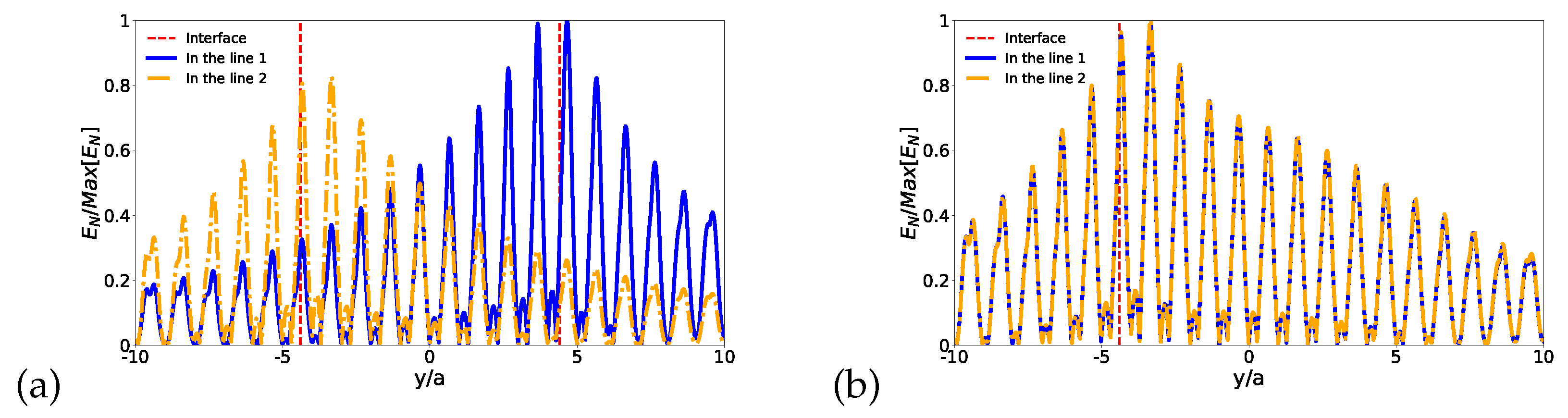
Before concluding, after studying the robustness of the edge modes, let us take look at the localization of the edge modes. In order to do so, we calculate point-by-point on a line perpendicular to the interface (the blue line in Figure 12 and Figure 13). Therefore in Figure 12 is shown the intensity of point-by-point along the line of the interface with no defect and with small defects: the interface with a cavity, the interface with a bigger rod, the interface with a disorder, and the interface with an Ag rod. The same is illustrated in Figure 13 for the extensive defects: the Z interface, and the Omega interface. We consider in all cases . From Figure 12(a)-Figure 12(e) we can infer that the electric field is localized around the interface, regardless of the small defect considered, i.e., the electric field is near zero in rods far from the interface for both cases: the topological and trivial photonic crystals. This corresponds to a topological insulator behavior of our system because it does not present fields in the bulk and the electric field is different from zero only around the interface [46,50,55]. For the special cases of extensive defects, i.e., the Z and Omega interfaces, we set two perpendicular lines: (i) one at the interface before the first change of orientation, and (ii) another at the interface after the second change of orientation (see Figure 13(a) and Figure 13(b)). As for the small defect cases, the interface modes are well localized. Notice that the normalized electric field rapidly goes to zero when the profile moves away from the interface for both, the Z and Omega interfaces. In short, in all defect cases considered here, the localization of the modes allows the confinement of the light, and the interface works as a waveguide for the propagation of electromagnetic waves. Finally, all those features described here make this system a good candidate for topological wave guides and open up an opportunity for phototransport applications.
6. Conclusions
In this work we have proposed a two-dimensional photonic crystal composed of dielectric cusped-oval-shaped rods (COS rods), in a triangular lattice with point symmetry group, with the unit cell composed of six COS rods. The band structure of the system was obtained through the software COMSOL Multiphysics, which is based on the finite element method (FEM). Our results show that, as we introduced an angular perturbation in the COS rods, a complete bandgap is opened in the band structure of the system. We have studied the topological phases of the system. It was found that for negative perturbations the photonic crystal is in a topological phase, while for positive perturbations the photonic crystal is in a trivial phase. The topological phase transition occurs for . We have also shown that the electromagnetic (EM) density energy distribution in the system can be used as a probe of the character of the band structure. This is because the EM density energy is proportional to the modulus square of the Wannier functions (WF) which are centered at the (maximal) localized Wyckoff positions (WP). Moreover, as a consequence of the perturbation, two edge states emerge inside the bandgap, which are localized around the interface and are topologically protected. Our results show that the edge modes are pseudospin modes traveling around the interface between the topological (negative perturbation) and trivial (positive perturbation) photonic crystals. They are topologically protected and robust against disorder and defects at the interface. For all defect cases considered in this work the transmittance is mildly affected. Therefore, the system studied is an excellent candidate for technological applications, once the flux of light can be controlled without any significant energetic loss or reflection. These features made the photonic crystal here proposed a good candidate to guide and confine light, with potential for phototransport applications.
Author Contributions
Conceptualization, D.B.-S., C.H.O.C., and C.G.B.; methodology, D.B.-S., C.H.O.C., and C.G.B.; software, D.B.-S., and C.H.O.C.; formal analyzis, D.B.-S., C.H.O.C., and C.G.B.; writing—original draft preparation, D.B.-S.; supervision, C.H.O.C., and C.G.B.; writing—review and editing, D.B.-S. and C.G.B. All authors have read and agreed to the published version of the manuscript.
Funding
This research was funded by Brazilian Research Agencies CNPq (Grant No. 309495/2021-0) and FUNCAP (Grant No. BP5-0197-00145.01.03/23). D.B.-S. acknowledges financial support from Brazilian Agency CAPES.
Data Availability Statement
The datasets generated during and/or analyzed during the current study are available from the corresponding author on reasonable request.
Acknowledgments
We thank G.M. Viswanathan for a critical reading of the manuscript.
Conflicts of Interest
The authors declare no conflict of interest.
References
- Joannopoulos, J.D.; Johnson, S.G.; Winn, J.N.; Meade, R.D. Photonic Crystals: Molding the Flow of Light, 2nd ed.; Princeton University Press: Princeton, NJ, USA, 2008; ISBN 978-0-691-12456-8. [Google Scholar]
- Yang, Z.; Lustig, E.; Lumer, Y.; Segev, M. Photonic Floquet topological insulators in a fractal lattice. Light Sci. Appl. 2020, 9, 128. [Google Scholar] [CrossRef] [PubMed]
- Xie, B.-Y.; Wang, H.-F.; Zhu, X.-Y.; Lu, M.-H.; Wang, Z.D.; Chen, Y.-F. Photonics meets topology. Opt. Express 2018, 26, 24531. [Google Scholar] [CrossRef] [PubMed]
- Raghu, S.; Haldane, F.D.M. Analogs of quantum-Hall-effect edge states in photonic crystals. Phys. Rev. A 2008, 78, 033834. [Google Scholar] [CrossRef]
- Liu, F.; Deng, H.-Y.; Wakabayashi, K. Topological photonic crystals with zero Berry curvature. Phys. Rev. B 2018, 97, 035442. [Google Scholar] [CrossRef]
- Dong, J.-W.; Chen, X.-D.; Zhu, H.; Wang, Y.; Zhang, X. Valley photonic crystals for control of spin and topology. Nat. Mater. 2017, 16, 298. [Google Scholar] [CrossRef] [PubMed]
- Xie, B.-Y.; Wang, H.-F.; Wang, H.-X.; Zhu, X.-Y.; Jiang, J.-H.; Lu, M.-H.; Chen, Y.-F. Second-order photonic topological insulator with corner states. Phys. Rev. B 2018, 98, 205147. [Google Scholar] [CrossRef]
- Wang, C.; Zhang, H.; Yuan, H.; Zhong, J.; Lu, C. Universal numerical calculation method for the Berry curvature and Chern numbers of typical topological photonic crystals. Front. Optoelectron. 2020, 13, 73. [Google Scholar] [CrossRef]
- Wang, Y.; Zhang, W.; Zhang, X. Tunable topological valley transport in two-dimensional photonic crystals. New J. Phys. 2019, 21, 093020. [Google Scholar] [CrossRef]
- Wu, S.; Jiang, B.; Liu, Y.; Jiang, J.-H. All-dielectric photonic crystal with unconventional higher-order topology. Photonics Res. 2021, 9, 668. [Google Scholar] [CrossRef]
- Wong, S.; Saba, M.; Hess, O.; Oh, S.S. Gapless unidirectional photonic transport using all-dielectric kagome lattices. Phys. Rev. Res. 2020, 2, 012011. [Google Scholar] [CrossRef]
- Mittal, S.; Orre, V.V.; Leykam, D.; Chong, Y.D.; Hafezi, M. Photonic Anomalous Quantum Hall Effect. Phys. Rev. Lett. 2019, 123, 043201. [Google Scholar] [CrossRef] [PubMed]
- Jahani, D.; Ghatar, A.; Abaspour, L.; Jahani, T. Photonic Hall effect. J. Appl. Phys. 2018, 124, 043104. [Google Scholar] [CrossRef]
- Xie, B.; Su, G.; Wang, H.-F.; Liu, F.; Hu, L.; Yu, S.-Y.; Zhan, P.; Lu, M.-H.; Wang, Z.; Chen, Y.-F. Higher-order quantum spin Hall effect in a photonic crystal. Nat. Commun. 2020, 11, 3768. [Google Scholar] [CrossRef] [PubMed]
- Chen, X.-D.; Deng, W.-M.; Shi, F.-L.; Zhao, F.-L.; Chen, M.; Dong, J.-W. Direct Observation of Corner States in Second-Order Topological Photonic Crystal Slabs. Phys. Rev. Lett. 2019, 122, 233902. [Google Scholar] [CrossRef] [PubMed]
- Zhang, L.; Yang, Y.; Lin, Z.-K.; Qin, P.; Chen, Q.; Gao, F.; Li, E.; Jiang, J.-H.; Zhang, B.; Chen, H. Higher-Order Topological States in Surface-Wave Photonic Crystals. Adv. Sci. 2020, 7, 1902724. [Google Scholar] [CrossRef] [PubMed]
- Wu, Y.; Hu, X.; Gong, Q. Reconfigurable topological states in valley photonic crystals. Phys. Rev. Materials 2018, 2, 122201. [Google Scholar] [CrossRef]
- Chen, M.L.N.; Jiang, L.J.; Lan, Z.; Sha, W.E.I. Coexistence of pseudospin- and valley-Hall-like edge states in a photonic crystal with C3v symmetry. Phys. Rev. Research 2020, 2, 043148. [Google Scholar] [CrossRef]
- Kim, M.; Kim, Y.; Rho, J. Spin-valley locked topological edge states in a staggered chiral photonic crystal. New J. Phys. 2020, 22, 113022. [Google Scholar] [CrossRef]
- Bleu, O.; Solnyshkov, D.D.; Malpuech, G. Quantum valley Hall effect and perfect valley filter based on photonic analogs of transitional metal dichalcogenides. Phys. Rev. B 2017, 95, 235431. [Google Scholar] [CrossRef]
- Wu, L.-H.; Hu, X. Scheme for achieving a topological photonic crystal by using dielectric material. Phys. Rev. Lett. 2015, 114, 223901. [Google Scholar] [CrossRef]
- Dai, H.; Liu, T.; Jiao, J.; Xia, B.; Yu, D. Double Dirac cone in two-dimensional phononic crystals beyond circular cells. J. Appl. Phys. 2017, 121, 135105. [Google Scholar] [CrossRef]
- Hajivandi, J.; Pakarzadeh, H.; Kurt, H. Intensity tuning of the edge states in the imperfect topological waveguides based on the photonic crystals with the C3 point group symmetry. Opt. Quantum Electron. 2021, 53, 102. [Google Scholar] [CrossRef]
- Khanikaev, A.B.; Shvets, G. Two-dimensional topological photonics. Nat. Photonics 2017, 11, 763. [Google Scholar] [CrossRef]
- Sauer, E.; Vasco, J.P.; Hughes, S. Theory of intrinsic propagation losses in topological edge states of planar photonic crystals. Phys. Rev. Res. 2020, 2, 043109. [Google Scholar] [CrossRef]
- Lu, L.; Joannopoulos, J.D.; Soljačić, M. Topological photonics. Nat. Photonics 2014, 8, 821. [Google Scholar] [CrossRef]
- Arregui, G.; Gomis-Bresco, J.; Sotomayor-Torres, C.M.; Garcia, P.D. Quantifying the robustness of topological slow light. Phys. Rev. Lett. 2021, 1. [Google Scholar] [CrossRef] [PubMed]
- Huang, H.; Huo, S.; Chen, J. Reconfigurable topological phases in two-dimensional dielectric photonic crystals. Crystals 2019, 9, 221. [Google Scholar] [CrossRef]
- Dresselhaus, M.S.; Dresselhaus, G.; Jorio, A. Group theory: application to the physics of condensed matter, 1st ed.; Springer-Verlag: Berlin, Germany, 2007; ISBN 978-3-540-32897-1. [Google Scholar]
- Yang, Y.; Xu, Y.F.; Xu, T.; Wang, H.-X.; Jiang, J.-H.; Hu, X.; Hang, Z.H. Visualization of a unidirectional electromagnetic waveguide using topological photonic crystals made of dielectric materials. Phys. Rev. Lett. 2018, 120, 217401. [Google Scholar] [CrossRef] [PubMed]
- COMSOL multiphysics. Available online: www.comsol.com/products/multiphysics/ (accessed on 6 June 2023).
- Fang, Y.; Wang, Z. Highly confined topological edge states from two simple triangular lattices with reversed materials. Opt. Commun. 2021, 479, 126451. [Google Scholar] [CrossRef]
- Deng, W.-M.; Chen, X.-D.; Zhao, F.-L.; Dong, J.-W. Transverse angular momentum in topological photonic crystals. J. Opt. 2018, 20, 014006. [Google Scholar] [CrossRef]
- Smirnova, D.; Leykam, D.; Chong, Y. , Kivshar, Y. Nonlinear topological photonics. Appl. Phys. Rev. 2020, 7, 021306. [Google Scholar] [CrossRef]
- Peng, Y.; Yan, B.; Xie, J.; Liu, E.; Li, H.; Ge, R.; Gao, F.; Liu, J. Variation of Topological Edge States of 2D Honeycomb Lattice Photonic Crystals. Phys. Status Solidi RRL 2020, 14, 2000202. [Google Scholar] [CrossRef]
- Li, Z.; Chan, H.-C.; Xiang, Y. Fragile topology based helical edge states in two-dimensional moon-shaped photonic crystals. Phys. Rev. B 2020, 102, 245149. [Google Scholar] [CrossRef]
- Alexandradinata, A.; Fang, C.; Gilbert, M.J.; Bernevig, B.A. Spin-Orbit-Free Topological Insulators without Time-Reversal Symmetry. Phys. Rev. Lett. 2014, 113, 116403. [Google Scholar] [CrossRef] [PubMed]
- de Paz, M.B.; Herrera, M.A.J.; Arroyo Huidobro, P.; Alaeian, H.; Vergniory, M.G.; Bradlyn, B.; Giedke, G.; García-Etxarri, A.; Bercioux, D. Energy density as a probe of band representations in photonic crystals. J. Phys.: Condens. Matter 2022, 34, 314002. [Google Scholar] [CrossRef]
- Marzari, N.; Mostofi, A.A.; Yates, J.R.; Souza, I.; Vanderbilt, D. Maximally localized Wannier functions: Theory and applications. Rev. Mod. Phys. 2012, 84, 1419. [Google Scholar] [CrossRef]
- Berry, M.V. Quantal phase factors accompanying adiabatic changes. Proc. R. Soc. Lond. A 1984, 392, 45. [Google Scholar] [CrossRef]
- Albert, J.P.; Jouanin, C.; Cassagne, D.; Monge, D. Photonic crystal modelling using a tight-binding Wannier function method. Opt. Quantum Electron. 2002, 34, 251. [Google Scholar] [CrossRef]
- Parappurath, N.; Alpeggiani, F.; Kuipers, L.; Verhagen, E. Direct observation of topological edge states in silicon photonic crystals: Spin, dispersion, and chiral routing. Sci. Adv. 2020, 6, eaaw4137. [Google Scholar] [CrossRef]
- Silveirinha, M.G. Bulk-edge correspondence for topological photonic continua. Phys. Rev. B. 2016, 94, 205105. [Google Scholar] [CrossRef]
- Ma, J.; Li, X.; Fang, Y. Embedded topological edge states from reversed two-dimensional photonic crystals. Physica E 2021, 127, 114517. [Google Scholar] [CrossRef]
- Yang, Y.; Yamagami, Y.; Yu, X.; Pitchappa, P.; Webber, J.; Zhang, B.; Fujita, M.; Nagatsuma, T.; Singh, R. Terahertz topological photonics for on-chip communication. Nat. Photonics 2020, 14, 446–10. [Google Scholar] [CrossRef]
- Ni, X.; Purtseladze, D.; Smirnova, D.A.; Slobozhanyuk, A.; Alù, A.; Khanikaev, A.B. Spin-and valley-polarized one-way Klein tunneling in photonic topological insulators. Sci. Adv. 2018, 4, eaap8802. [Google Scholar] [CrossRef]
- Arora, S.; Bauer, T.; Barczyk, R.; Verhagen, E.; Kuipers, L. Direct quantification of topological protection in symmetry-protected photonic edge states at telecom wavelengths. Light Sci. Appl. 2021, 10, 9. [Google Scholar] [CrossRef]
- Huang, H.; Huo, S.; Chen, J. Subwavelength elastic topological negative refraction in ternary locally resonant phononic crystals. Int. J. Mech. Sci. 2021, 198, 106391. [Google Scholar] [CrossRef]
- Chen, X.-D.; Shi, F.-L.; Liu, H.; Lu, J.-C.; Deng, W.-M.; Dai, J.-Y.; Cheng, Q.; Dong, J.-W. Tunable Electromagnetic Flow Control in Valley Photonic Crystal Waveguides. Phys. Rev. Applied 2018, 10, 044002. [Google Scholar] [CrossRef]
- Chen, X.-D.; Zhao, F.-L.; Chen, M.; Dong, J.-W. Valley-contrasting physics in all-dielectric photonic crystals: Orbital angular momentum and topological propagation. Phys. Rev. B 2017, 96, 020202. [Google Scholar] [CrossRef]
- He, X.-T.; Liang, E.-T.; Yuan, J.-J.; Qiu, H.-Y.; Chen, X.-D.; Zhao, F.-L.; Dong, J.-W. A silicon-on-insulator slab for topological valley transport. Nat. Commun. 2019, 10, 872. [Google Scholar] [CrossRef] [PubMed]
- Borges-Silva, D.; Costa, C.H.; Bezerra, C.G. Topological phase transition and robust pseudospin interface states induced by angular perturbation in 2D topological photonic crystals. Sci. Rep. 2023, 1. [Google Scholar] [CrossRef]
- Borges-Silva, D.; Costa, C.H.; Bezerra, C.G. Pseudospin topological behavior and topological edge states in a two-dimensional photonic crystal composed of Si rods in a triangular lattice. Phys. Rev. B 2023, 1. [Google Scholar] [CrossRef]
- Gong, Y.; Wong, S.; Bennett, A.J.; Huffaker, D.L.; Oh, S.S. Topological insulator laser using valley-Hall photonic crystals. ACS Photonics 2020, 7, 2089. [Google Scholar] [CrossRef]
- Mittal, S.; DeGottardi, W.; Hafezi, M. Topological photonic systems. Optics and Photonics News 2018, 29, 36. [Google Scholar] [CrossRef]
Figure 1.
Schematic illustration of the unit cell of the unperturbed PC composed of six COS Si rods surrounded by air. Here , is the distance from the center of the unit cell to the center of the rods, is the radius of the original cylindrical rods, and is the shift of the original rods.
Figure 1.
Schematic illustration of the unit cell of the unperturbed PC composed of six COS Si rods surrounded by air. Here , is the distance from the center of the unit cell to the center of the rods, is the radius of the original cylindrical rods, and is the shift of the original rods.
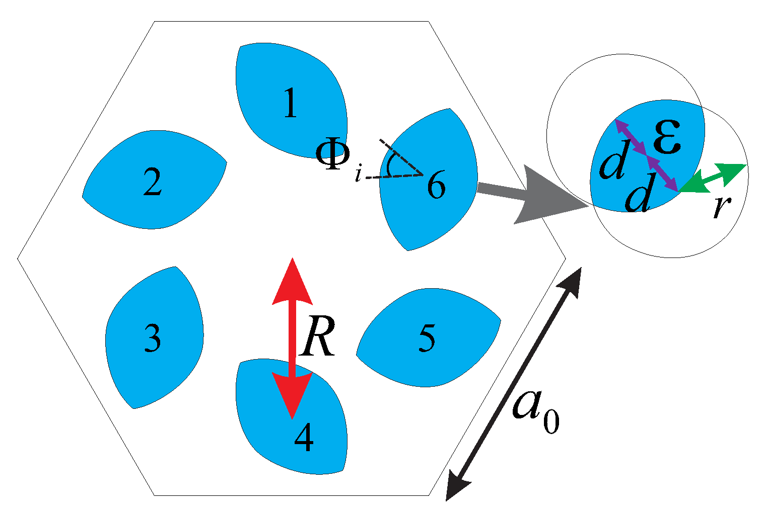
Figure 2.
Results for the unperturbed photonic crystal. (a) Band structure for the TM modes with , , , , , and . A doubly degenerate Dirac point is located at the point with . (b) Profile of at the Dirac point. We can see that the orbitals are dipole modes ( and ), and quadrupole modes ( and ).
Figure 2.
Results for the unperturbed photonic crystal. (a) Band structure for the TM modes with , , , , , and . A doubly degenerate Dirac point is located at the point with . (b) Profile of at the Dirac point. We can see that the orbitals are dipole modes ( and ), and quadrupole modes ( and ).
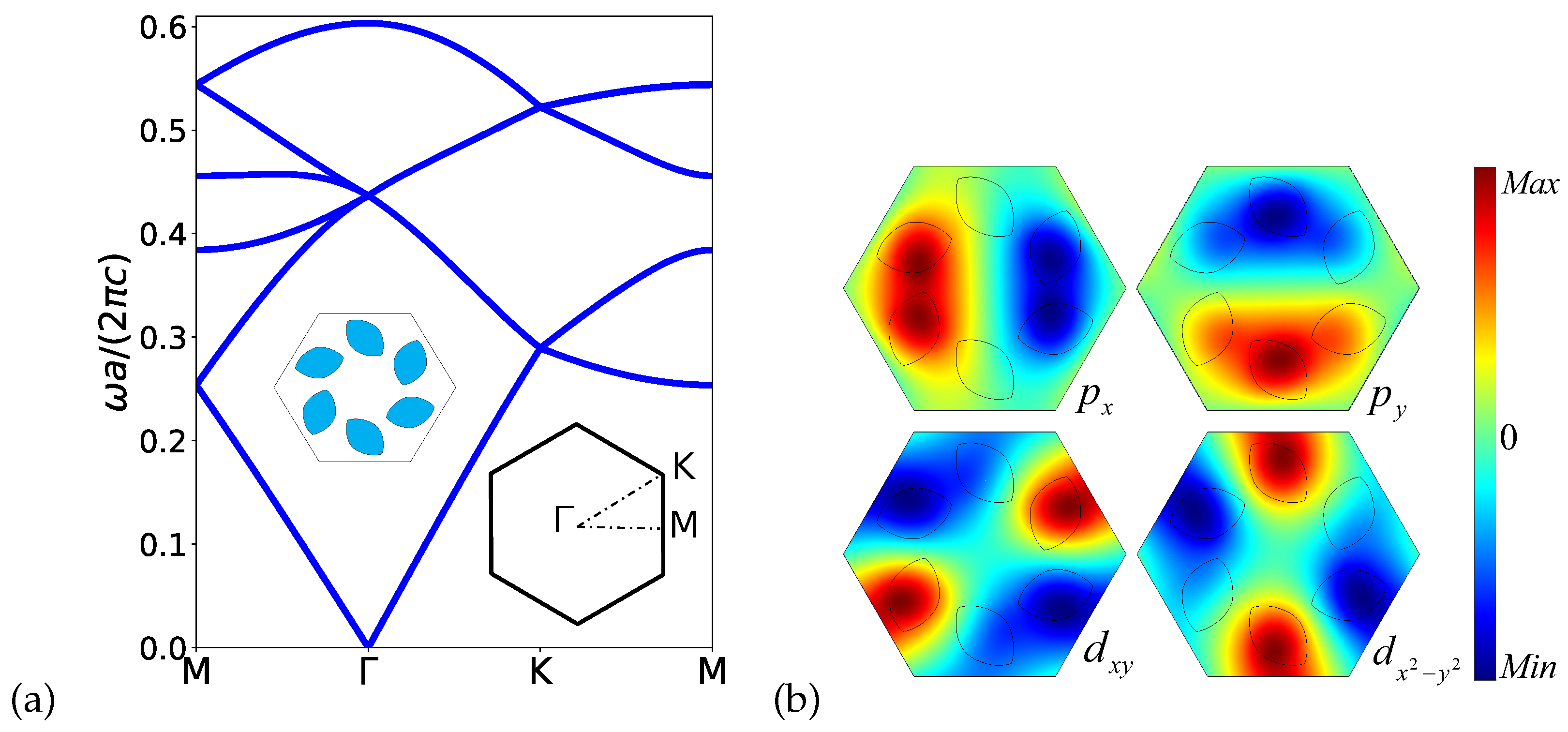
Figure 3.
Effect of the angular perturbation on the TM band structure at the point. It is possible to observe that the double degeneracy is lifted when we introduce a nonzero perturbation (see the main text).
Figure 3.
Effect of the angular perturbation on the TM band structure at the point. It is possible to observe that the double degeneracy is lifted when we introduce a nonzero perturbation (see the main text).
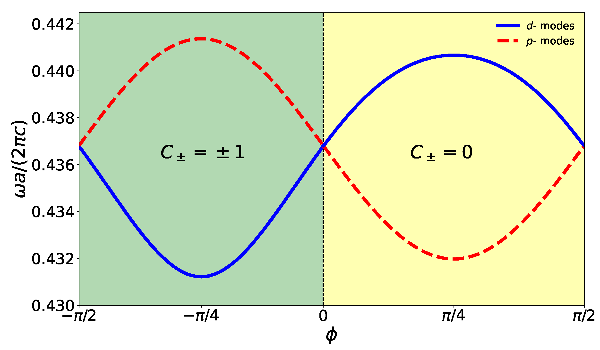
Figure 4.
Results for the perturbed photonic crystal. Band structure of the TM modes with , , , , and , for (a) the negative case () and (b) the positive case (), respectively. The bandgap is highlighted by the yellow area.
Figure 4.
Results for the perturbed photonic crystal. Band structure of the TM modes with , , , , and , for (a) the negative case () and (b) the positive case (), respectively. The bandgap is highlighted by the yellow area.
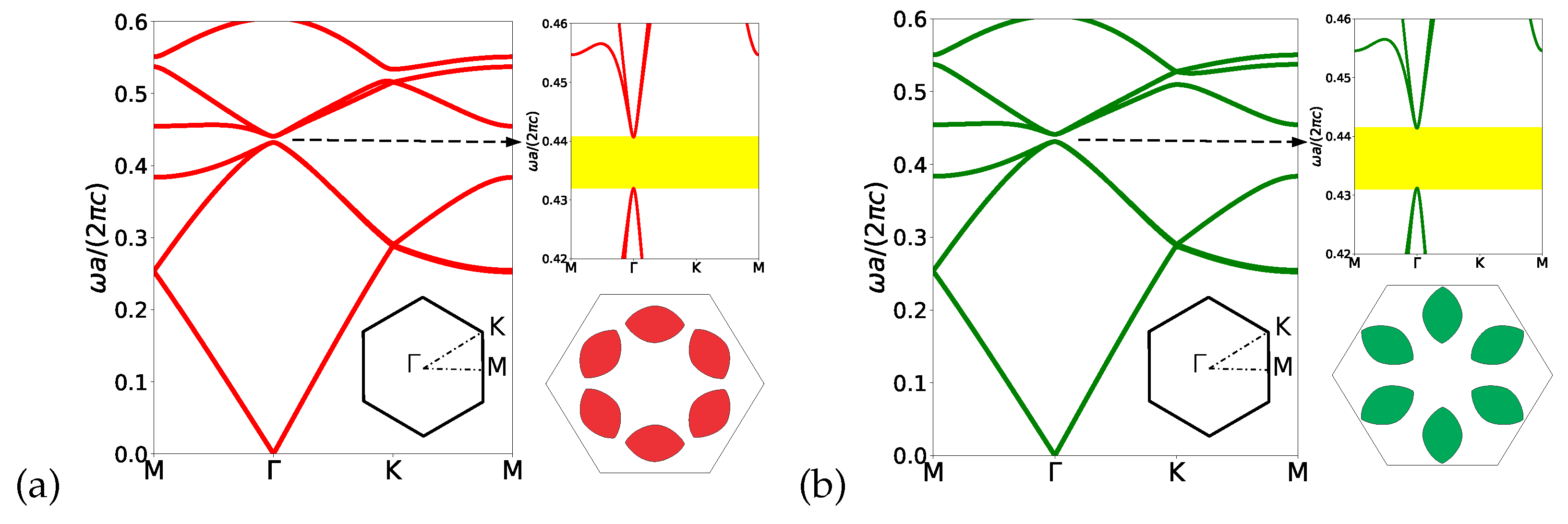
Figure 5.
Topological phase transition diagram. Profile of the electric field of the degenerate bands. There is an inversion of the bands between and . The left side represents the topological case, and the right side represents the trivial case. The topological phase transition occurs when .
Figure 5.
Topological phase transition diagram. Profile of the electric field of the degenerate bands. There is an inversion of the bands between and . The left side represents the topological case, and the right side represents the trivial case. The topological phase transition occurs when .
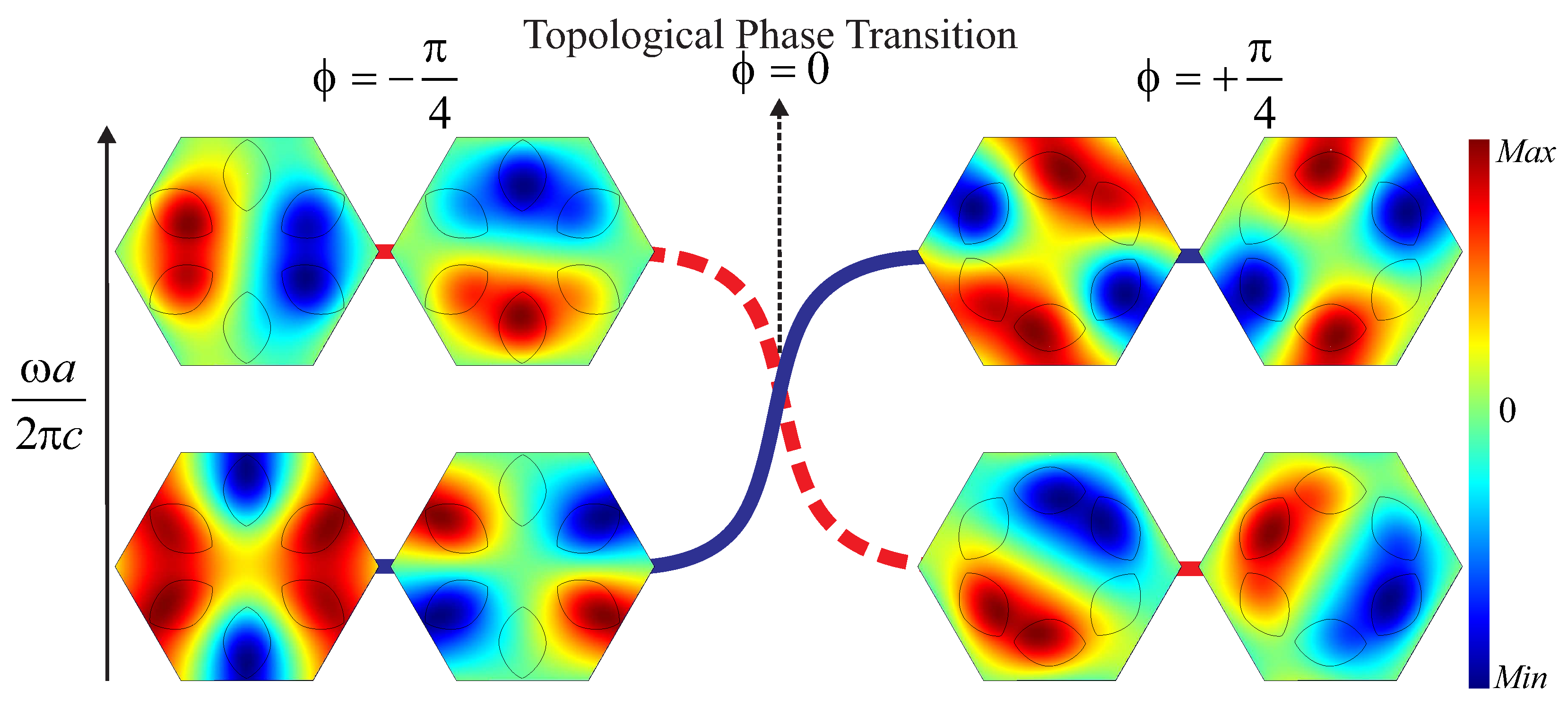
Figure 6.
Energy density distribution for TM modes with , , , , and for the (a) negative case (), and (b) positive case (). The positions of the maximal WP , and are also illustrated.
Figure 6.
Energy density distribution for TM modes with , , , , and for the (a) negative case (), and (b) positive case (). The positions of the maximal WP , and are also illustrated.
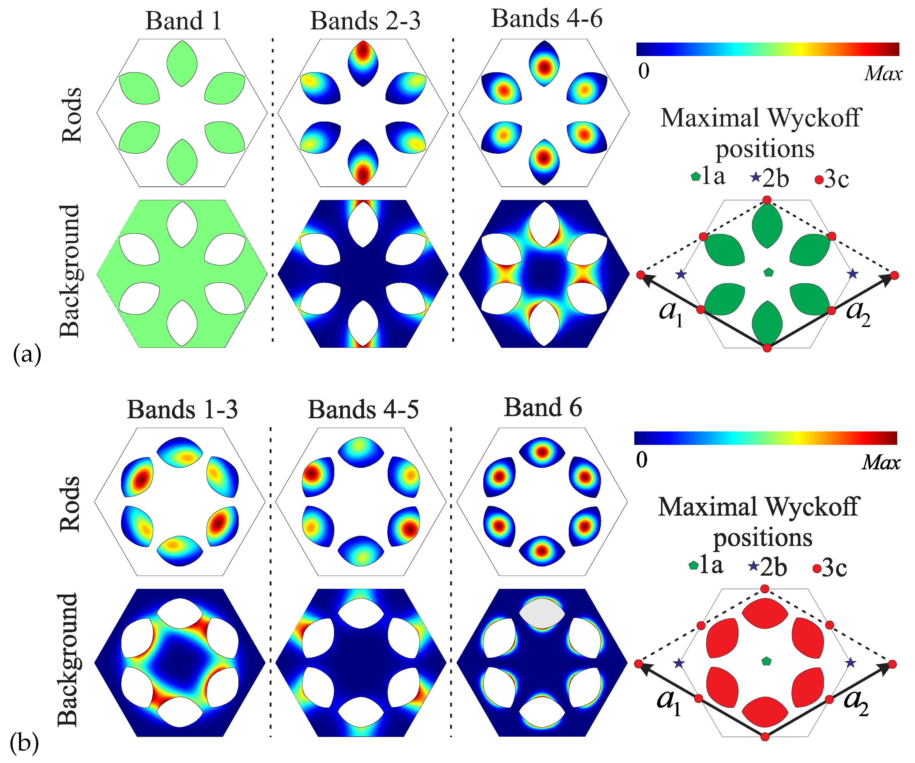
Figure 7.
for TM modes with , , , , and for (a) along the direction , (b) along the direction , (c) along the direction , (d) along the direction . The gray areas denote the rods.
Figure 7.
for TM modes with , , , , and for (a) along the direction , (b) along the direction , (c) along the direction , (d) along the direction . The gray areas denote the rods.
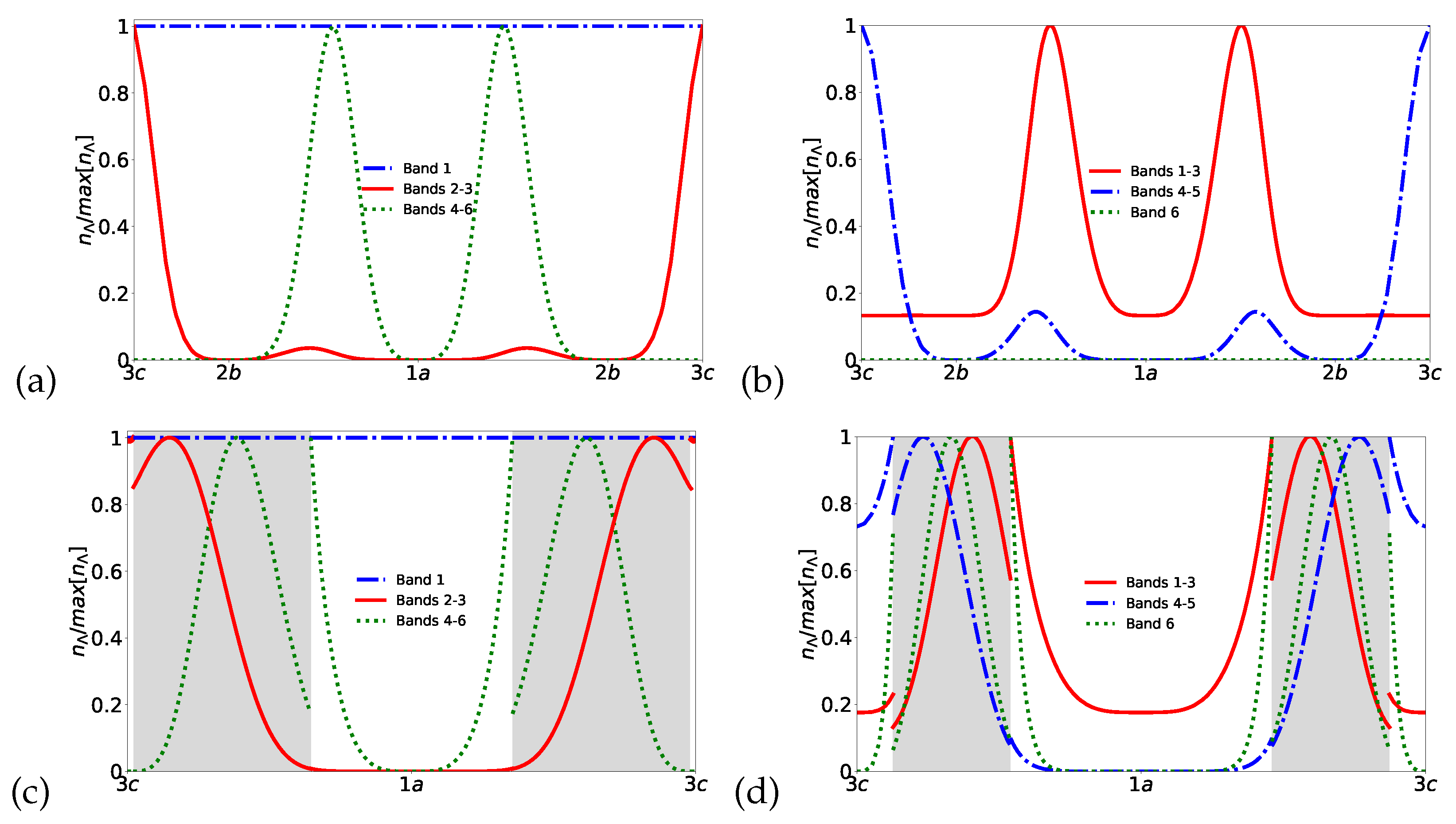
Figure 8.
(a) Projected band structure along the direction for TM modes of a supercell composed of 15 topological unit cells () and 15 expanded unit cells () making a horizontal interface. (b) - (c) , the phase of (the left panel), and the Poynting vector (the right panel) for (b) and for (c) at .
Figure 8.
(a) Projected band structure along the direction for TM modes of a supercell composed of 15 topological unit cells () and 15 expanded unit cells () making a horizontal interface. (b) - (c) , the phase of (the left panel), and the Poynting vector (the right panel) for (b) and for (c) at .
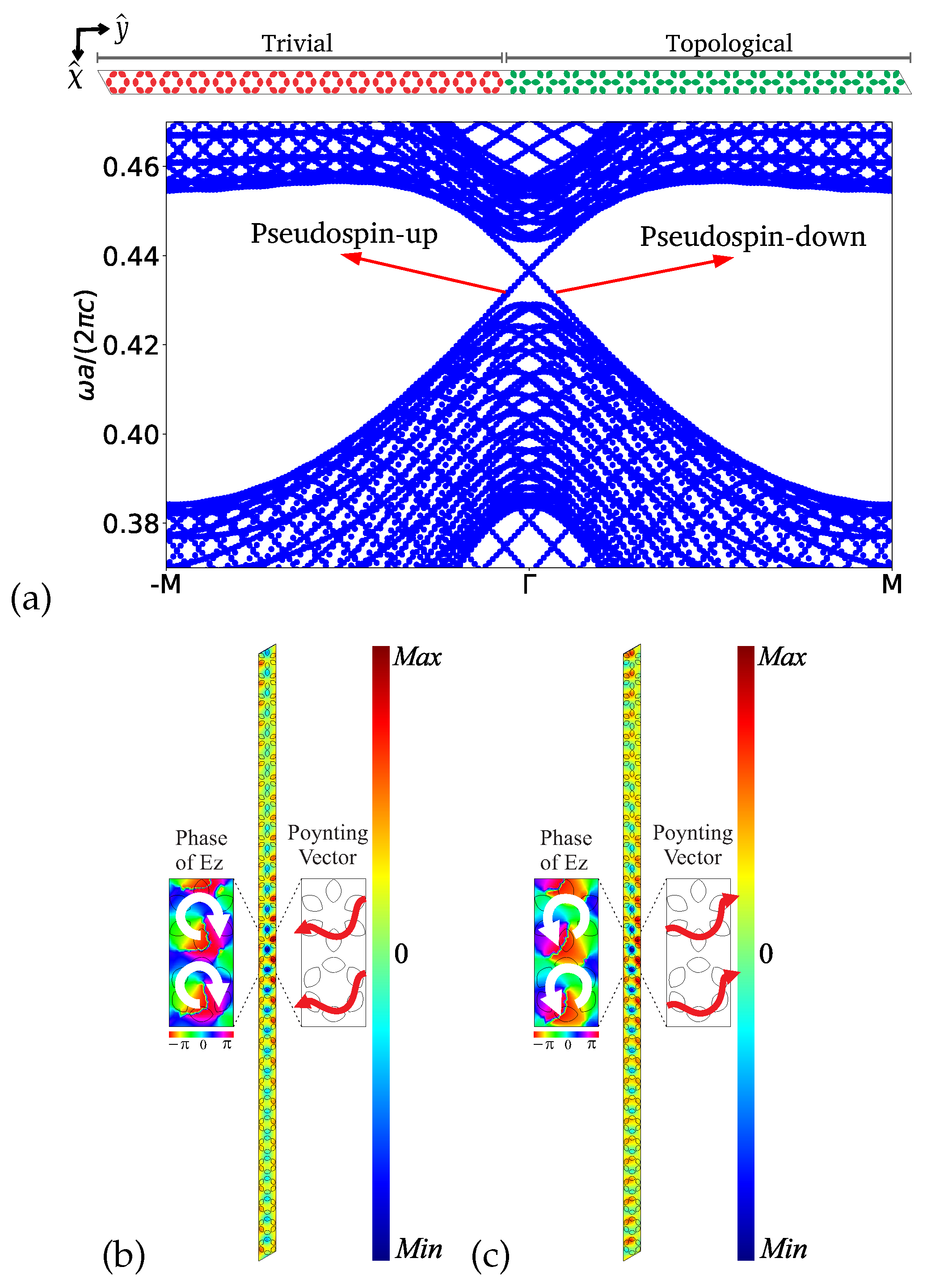
Figure 9.
Left panels: schematic illustration of the interface between topological and trivial photonic crystals, and , respectively. The source of light is on the left (purple arrow) and the detector of light is on the right (blue arrow). We build an (a) interface with no defect, (c) interface with a small cavity, (e) interface with a bigger rod (), (g) interface with an Ag rod (the yellow one), and (i) interface with a disorder. Right panels: distribution of the normalised electric field and Poynting vector (red arrows in the zoom area around the defects) for for the (b) interface with no defect, (d) interface with a small cavity, (f) interface with a bigger rod, (h) interface with an Ag, and (j) interface with a disorder.
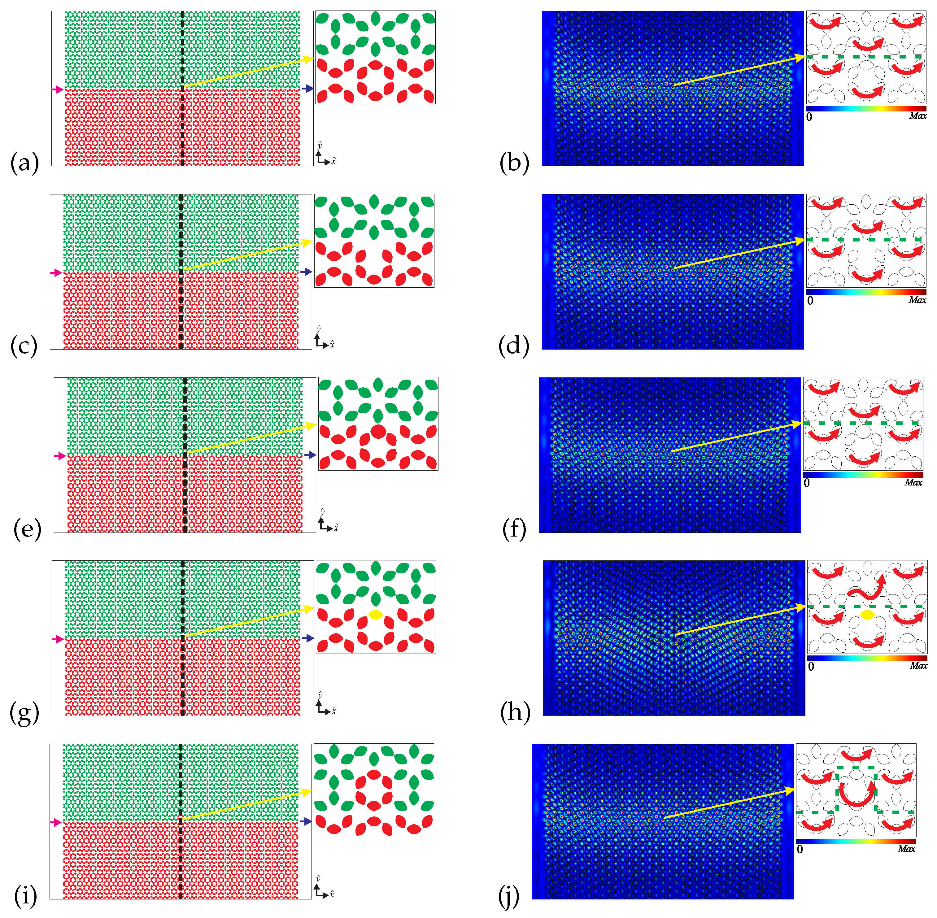
Figure 10.
Left panels: schematic illustration of the interface between topological and trivial photonic crystals, and respectively. The source of light is on the left (purple arrow) and the detector of light is on the right (blue arrow). We build a (a) Z interface and an (c) Omega interface. Right panels: distribution of the normalised electric field and Poynting vector (red arrows in the zoom area around the defects) to to the (b) Z interface, (d) Omega interface.
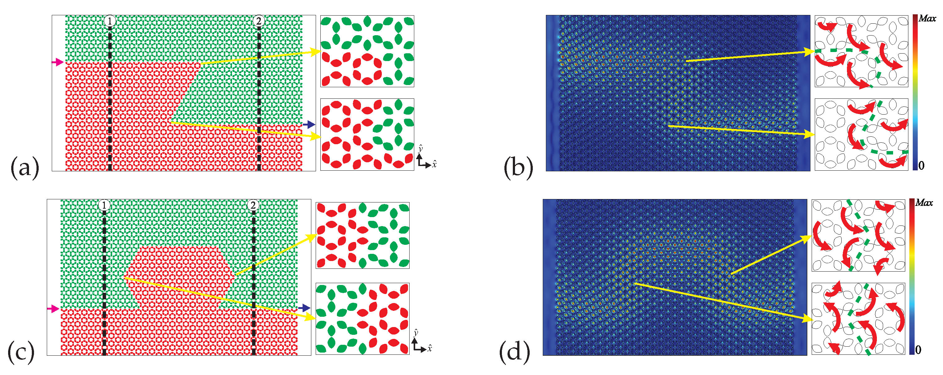
Figure 11.
Transmittance for the cases without defect, with a small cavity, with a bigger rod, with a disorder in the interface, with an Ag rod, with a Z interface, and an Omega interface. We can observe that the transmittance is around 1.0 even for the configurations with defects.
Figure 11.
Transmittance for the cases without defect, with a small cavity, with a bigger rod, with a disorder in the interface, with an Ag rod, with a Z interface, and an Omega interface. We can observe that the transmittance is around 1.0 even for the configurations with defects.
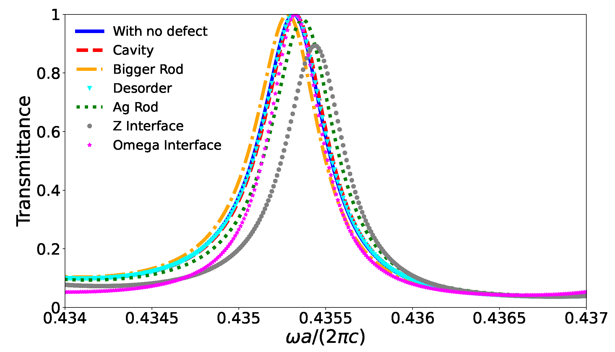
Figure 12.
Intensity of vs y () for (a) interface with no defect, (b) interface with a small cavity, (c) interface with a bigger rod, (d) interface with an Ag rod, and (e) interface with a disorder.
Figure 12.
Intensity of vs y () for (a) interface with no defect, (b) interface with a small cavity, (c) interface with a bigger rod, (d) interface with an Ag rod, and (e) interface with a disorder.
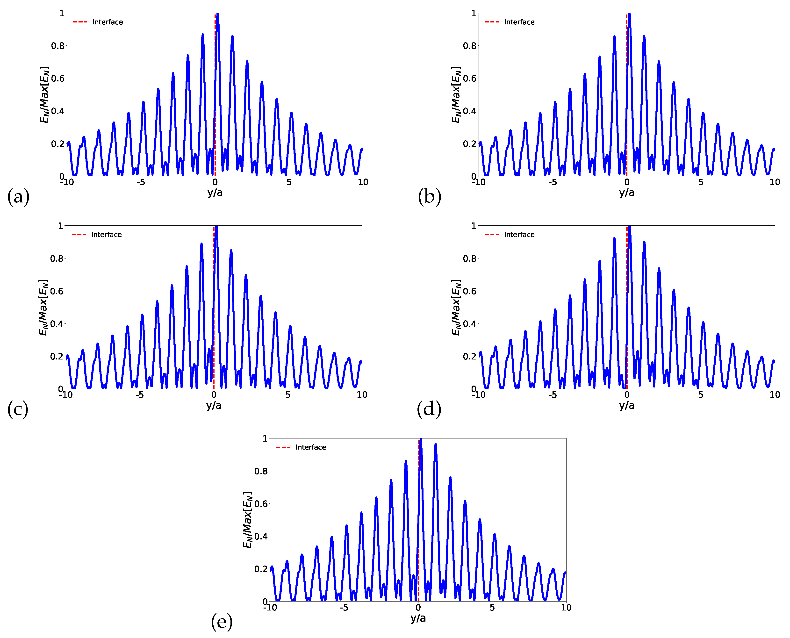
Figure 13.
Intensity of vs y () for the (a) Z interface, and (b) Omega interface.
Disclaimer/Publisher’s Note: The statements, opinions and data contained in all publications are solely those of the individual author(s) and contributor(s) and not of MDPI and/or the editor(s). MDPI and/or the editor(s) disclaim responsibility for any injury to people or property resulting from any ideas, methods, instructions or products referred to in the content. |
© 2023 by the authors. Licensee MDPI, Basel, Switzerland. This article is an open access article distributed under the terms and conditions of the Creative Commons Attribution (CC BY) license (http://creativecommons.org/licenses/by/4.0/).
Copyright: This open access article is published under a Creative Commons CC BY 4.0 license, which permit the free download, distribution, and reuse, provided that the author and preprint are cited in any reuse.


