
Submitted:
18 July 2023
Posted:
19 July 2023
You are already at the latest version
Abstract
This paper presents the design of a miniaturized polyimide-based antenna for Ultra-Wideband (UWB) communication. Miniaturization is achieved through the utilization of adhesive material with a high dielectric constant (high-Dk). The goal of this work is to investigate the impact of such material on the antenna performance and to optimize its design for UWB operation. The manufacturing of the antenna using the proposed structure was developed and the prototype of antenna for UWB high-band (6 - 9 GHz) is measured and analyzed. By leveraging the high Dk of the adhesive material, the simulation and measurement results showed that the proposed antenna with high Dk adhesive film can achieve the compact dimension with good performance in gain, and time domain characteristics. The results of this study show a potential of exhibiting a reduction in the size of the antenna and will contribute to the advancement of miniaturized UWB antenna technology.
Keywords:
UWB
; high-Dk adhesive
; monopole antenna
; thin film antenna
1. Introduction
Ultra-Wideband (UWB) technology has increasingly aroused a lot of interest in many applications of high-speed wireless communication and accurate localization [1,2]. With the characteristic of wide bandwidth, UWB systems have the advantages of improvement in multi-path fading immunity, enhancement in ranging resolution, great ability of objective penetration, and large tolerance to interference with other wireless systems [2].
In UWB system, antenna is one of the most essential elements as it is responsible for transmitting and receiving signals. In the antenna design process for the UWB system, miniaturization is a challenge due to the physical size constraints imposed by their applications. In [3,4,5], antennas with monopole structure and Vivaldi structure are suggested for UWB systems. However, they have no flexible capabilities. On the other hand, the interest in research on flexible electronics has increased in response to the commercial trends in compact, portable, lightweight, and flexibility [6]. Several approaches for flexible printed circuit (FPC) antennas have been reported.
In [7], a tapered slot antenna using a 200 m liquid crystal polymer (LCP) substrate is proposed. The design shows great radiation performance and excellent time-domain characteristics as very little distortion is introduced by the antenna. However, the bulky dimensions () are not suitable for modern electronics integration. In [8], an elliptical-shaped monopole UWB antenna printed on Kapton polyimide substrate is presented. It shows good radiation characteristics and impedance matching, with low degradation when under bending effects. However, the size of it () needs further miniaturized.
In [9], H. Bahrami et al. has designed flexible spiral-type dual-polarization antennas for neural recording systems by using a substrate of polyimide (PI) with a dielectric constant (Dk) of 3.5. In [10], a CPW-fed monopole with dimensions of for wearable application is suggested. Polyester with Dk = 3.2 is used as an antenna substrate, and polydimethylsiloxane (PDMS) with Dk = 2.3 - 2.8 is used as an artificial magnetic conductor (AMC). In [11], Hong et al. proposed a design of transparent and flexible antenna with ITO/Ag/ITO (IAI) multilayer for wearable glasses application. The PI film layer with Dk = 3.5 is chosen as the substrate. Phan et al. designed a microstrip monopole antenna "Sapin" covering the bandwidth from 2.2 - 10 GHz for wireless Local Area Network (WLAN) application [12]. The antenna dimension is and the substrate is E4D paper with Dk = 3.184. In [13], an inverted-F structure with a bow-tie shape is suggested for wearable applications with the substrate consisting of two-layer PI with Dk of 3.5. Of all these works, low-Dk film materials are often chosen as the antenna’s substrate because low-Dk material allows energy to be radiated out of the system, rather than being stored in the substrate, which results in increasing the bandwidth of resonance. However, to overcome the space limitation, one approach to miniaturization is to use a high-Dk substrate with the scarification of bandwidth.
Flexible Copper-Clad Laminate (FCCL) is usually used as the base material to create FPCs. FCCL consists layers of copper foil, PI film and bonding adhesive, providing the advantages such as high thermal stability and resistance to environmental factors [14]. Film material, however, usually has a low Dk. In the structure of a thin film antenna, the thickness of the bonding adhesive layer is comparable with the PI layer, therefore, its impact can be significant to the antenna’s performance. Current technologies are focusing on making low dielectric constant (low-Dk) and low dielectric dissipation (low-Df) adhesive bonding film for utilizing resonant bandwidth. To the best of the authors’ knowledge, none of the existing research has investigated the effect of the adhesive layer on the performance of the antenna. Hence, for the first time, the utilization of a high-Dk bonding adhesive in the design and construction of the antenna is explored. By investigating the overall performance, valuable insights can be acquired to study the efficiency and potential of using high-Dk adhesive for thin film antennas. Besides the physical size constraint, other parameters must also be considered in the designing process of UWB antennas such as wide bandwidth, stable pattern characteristics, and good time-domain performance [15].
In this paper, we propose a design of antenna for UWB using a new adhesive material with high-Dk and low-Df, showing that using such material could reduce the overall size of antenna while remaining the desired UWB characteristics. First, the antenna design for the high band of UWB (6 - 9 GHz) using high-Dk, low-Df bonding sheet adhesive will be designed and parametric studies of important parameters are presented in Section 2. Next, the antenna fabrication and experimental results including radiation pattern, reflection coefficient, and gain are simulated and measured in Section 3. In Section 4, the time domain analysis is presented. Discussion and comparison with other existing flexible antennas will be presented and the final conclusion is stated in Section 5.
2. Design of thin film UWB monopole antenna
2.1. Thin film layer stack up
The target operation frequency range of the proposed thin film UWB antenna is 6 - 9 GHz which is the UWB high-band for indoor UWB transmissions when no mitigation techniques are used [16]. Among a variety of UWB antenna structures, a bell shape monopole antenna was chosen as shown in Figure 1 since this structure is compatible with thin films, and offers broadband impedance matching and omnidirectional radiations [17,18,19]. The stack up of the thin film is also depicted in Figure 1. It consists of top and bottom copper layers deposited on PI layers. These a pair of copper/PI layer is bonded together by the middle adhesive layer which exhibits a high Dk property in this proposed design. The Dk and Df of the PI layer is 3.3 and 0.005, respectively, while the Dk and Df of the adhesive layer is 6 and 0.006. The thicknesses of copper, PI and adhesive layers are 12 m, 50 m and 50 m. The total thickness of the antenna combination is 174 m. It is worth noting that the thickness of one layer of copper and adhesive is the same while the Dk of adhesive layer is 1.8 times higher than PI. Thus, the high Dk property of the adhesive layer is supposed to promote thin film antenna miniaturization similar to previous reports on PCB antenna miniaturization using high Dk substrates [20,21,22].
2.2. Simulation results
Figure 1 shows the geometry of the proposed printed monopole antenna backed by a partial ground plane, where and are the width and length of the antenna, respectively. The dimension of the proposed antenna is . The ground of the antenna is designed based half elliptical shape with the vertex length of and is the aspect ratio of the ellipse, which is the ratio between the length of the major axis and the minor axis. The radiator patch is determined by the width of and the length of the patch is a combination of a straight line with a length of and a curve which is drawn by using the spline function. and are the length and width of the transmission line. A small rectangular with the width of is placed at the starting point of the feed line for soldering with a SubMiniature version A (SMA) connector. Table 1 shows the list of these parameters and their optimized value.
Figure 2 presents the simulation results of the of the antenna while changing some key parameters in the designing process. The refers to the reflection coefficient of the antenna and indicates the amount of power that is reflected back toward the source when an electromagnetic signal is transmitted through the antenna. To improve the impedance and radiation properties, a partial ground is designed. The effects of length are analyzed as in Figure 2a. As we can see, the smaller ground plane’s length will result in poor impedance matching results and with the longer ground plane’s length, the resonant frequency will shift to a lower frequency. It is worth noting that the increase in the ground plane’s length will result in a smaller gap between the antenna’s patch and the ground. With of 7.7 mm, this gap is so small that the bandwidth gets narrower. Only the ground length of 7.3 mm meets the required < -10 dB over an interested frequency bandwidth of 6 - 9 GHz. Hence, 7.3 mm is chosen as the value of .
Figure 2b shows how the length of the straight patch influences the magnitude of reflection coefficient over frequency. As can be seen, when the patch gets longer, resonant frequency tends to move towards the lower band. This can be explained that the longer patch length results in a longer electrical length and the propagation occurs in a longer wavelength, meaning the lower resonant frequency. Moreover, the > -10 dB around the mid-band of UWB is recorded in shorter patch length. On the other hand, with of 6.7 mm, a good < -10 dB is provided for our interested frequency band 6 - 9 GHz. For this reason, the appropriated value is chosen as 6.7 mm. To verify the theoretical results, the following section will address this with experiments.
3. Antenna fabrication and measurements
A photograph of the fabricated antenna with the front and back view is shown in Figure 3. For experimental measurement, our antenna requires connection to a Vector Network Analyzer (VNA) via a connector. The part number of the SMA connector used is Board Edge SMA SM06FS006 of Withwave company. Its operating frequency is from 10 MHz to 26.5 GHz with 50 matched. From Figure 4, we can notice some agreements of reflection coefficient between the simulation and measurement. Both the simulated and measured results have a bandwidth of more than 6 - 9 GHz for < - 10 dB, which is satisfied our target frequency band for the high band of UWB. The measurement impedance bandwidth is recorded from 5 - 10.8 GHz. The discrepancy in simulation and measurement results is from the widened ground effect due to the SMA connector, which is neglected in the simulation environment.
For the far-field gain experiment, the antenna measurement was done in an anechoic chamber. Figure 5 shows the picture of the fabricated antenna in the chamber while doing measurements. Figure 6 shows the comparison between simulation and measurement results in terms of normalized radiation patterns in the H-plane, which is the XY-plane ( = 90), and E-plane, which is the XZ-plane ( = 0) of the designed antenna operating at the frequency of 6 GHz and 7.5 GHz. Apparently, the omnidirectional radiation pattern in the E-plane (XZ-plane) and the form of figure-eight shape in the H-plane (XY-plane) are provided. It is worth noting that the measurement results do include the effect of cable and connector, which impacts results.
Figure 7 shows the peak gain of the fabricated antenna in simulation and experiment in XZ-plane ( = 0). The measured gain has a very similar trend to the simulated gain. However, it is lower than that in simulation, this can be explained by the loss of cable, connector and the chamber is not calibrated effectively. The average measured peak gain is about 2.1 dB over the frequency band, and the maximum peak gain of 2.8 dB is measured at 8 GHz, which is 3.6 dB in the simulation. The antenna gain is acceptable for an omnidirectional radiated antenna. The measurement results in the time domain of the proposed antenna will be discussed in the following section.
4. Time domain analysis
This section will analyze the pulse-shape preservation capabilities of the antenna. In the ideal case, the received UWB pulse should have the same shape as the transmitted pulse. Therefore, the antenna design process should consider this to minimize the distortion effects produced by the antenna itself and the environment.
To analyze the time domain performance, the common approach is to consider the antenna as a linear time-invariant (LTI) system described by its transfer function or transmission parameter [23,24,25]. The measurement with a VNA is set up inside an anechoic chamber. For setting up the time domain analysis, the two identical prototypes of proposed antenna are arranged at a distance of 100 mm. Figure 8 shows three distinct configurations for time domain measurement: side by side, face by face, and face by side. The time domain measurement setup is shown in Figure 9.
The system transfer functions of the antenna systems of two identical antennas will be presented and analyzed. In order to transmit pulses without any distortion, the system transfer function should be constant over the desired frequency. By plotting both magnitude and phase, we can quantify the pulse distortion effects based on their linearity characteristics. Figure 10 shows the measured magnitude and phase results of for three configurations. It can be observed that the magnitude is quite stable and the phase response is linear over the frequency range of 6 - 9 GHz, which signifies that the pulse shape is preserved without any out-of-phase components.
For analyzing the pulse shape preservation capability of the antennas, the Square-Root Raised Cosine Signal (SRRC) pulse is chosen as the input pulse for its bell-shaped energy distribution across frequency range [26]. The mathematical form of the SRRC pulse is shown in (1):
where is the roll-off factor for bandwidth control, t is the time, and = 1/, is the symbol rate.
Figure 11 shows the amplitude-modulated SRRC pulse and its power spectrum density corresponding with the UWB indoor spectrum mask. The roll-off factor and the symbol rate of the modulated SRRC pulse are 0.4 and 10 GHz, respectively. The center frequency of the input pulse is chosen as 7.5 GHz, with the bandwidth covering the high band of UWB 6 - 9 GHz.
Figure 12 represents the pulse shape comparison of the modulated SRRC input pulse and received pulses in three configurations. The received signals are calculated by multiplying the original input signal with the transfer function in the frequency domain and then applying an inverse Fourier transform to get them back to the time domain. The received signals in the three configurations are almost identical, showing the consistency of the pulse preservation capability of proposed antennas in the omnidirectional plane of antennas.
To further investigate the equivalence between the transmitted and received waveform, the fidelity factor can be calculated as (2):
where and are two signals to be compared. The fidelity factor is done by taking the cross-correlation between 2 normalized signals when they are overlapped [27,28]. A fidelity factor of 1 means that the transmitted pulse and the received pulse are identical, there is no distortion during transmission. Meanwhile, the fidelity factor equals 0 indicating that the two signals are completely different. Table 2 shows the fidelity factor of antennas of three configurations. The results show that the fidelity is greater than 0.85, validating that the proposed antenna does not distort the signal pulse significantly.
The group delay shows the time delay of specific frequency components when traveling through a device. If the signal only contains one frequency component, which is a perfect sine-wave, the whole signal would experience a stable group delay. The UWB antenna; however, consists of numerous frequency components. In order to avoid being delayed differently at different frequencies, a linear phase response is required. This means a stable group delay over frequency is mandatory in UWB systems to satisfy the ideal case of pulse reservation condition [29].
In simple terms, group delay is the rate of change of phase shift with respect to frequency. It delay can be expressed mathematically as the negative derivative of phase response with respect to frequency :
The measured group delay is presented in Figure 13. We can recognize a quite stable group delay in three configurations at desired frequency band. Hence, the proposed antenna has been determined to be suitable for UWB communications.
5. Conclusions
The proposed antenna is compared with other existing flexible antennas in Table 3. Both absolute size and electrical size are presented, showing that the proposed antenna has a relatively compact dimension with a very thin thickness and the proposed antenna can operate with the bandwidth to cover the UWB high band. The free space wavelength is chosen with respect to the lower frequency of the frequency band. The maximum gain is lower than some works due to the trade-off with a smaller size, but it is acceptable for such a monopole antenna with omnidirectional radiation patterns.
To summarize, in this paper, a miniaturized antenna thin film antenna using a new high-Dk adhesive material is designed and fabricated for UWB communication. The antenna features a compact dimension of with the thickness of 174 m and exhibits a wide impedance bandwidth covering from 5 - 10.8 GHz. The experimental results closely align with the simulations, demonstrating excellent agreement. Additionally, the proposed antenna demonstrates favorable time-domain performance. This work gains insights into achieving the thin film compact antennas by manipulating the adhesive layer’s characteristics.
Funding
This work was supported in part by Basic Science Research Program through NRF funded by the Ministry of Education (NRF-2019R1A6A1A03032119) and in part by the Technology development Program (S3238198) funded by the Ministry of SMEs and Startups (MSS, Korea).
Conflicts of Interest
The authors declare no conflict of interest.
References
- Elsanhoury, M.; Mäkelä, P.; Koljonen, J.; Välisuo, P.; Shamsuzzoha, A.; Mantere, T.; Elmusrati, M.; Kuusniemi, H. Precision Positioning for Smart Logistics Using Ultra-Wideband Technology-Based Indoor Navigation: A Review. IEEE Access 2022, 10, 44413–44445. [Google Scholar] [CrossRef]
- Zafari, F.; Gkelias, A.; Leung, K.K. A Survey of Indoor Localization Systems and Technologies. IEEE Communications Surveys & Tutorials 2019, 21, 2568–2599. [Google Scholar] [CrossRef]
- Jeon Gwang-Hun, Dzagbletey Philip Ayiku, C. J.Y. A Cross-Joint Vivaldi Antenna Pair for Dual-Pol and Broadband Testing Capabilities. J. Electromagn. Eng. Sci 2021, 21, 201–209. [Google Scholar] [CrossRef]
- Mekki Kawther, Necibi Omrane, L. S.G.A. A UHF/UWB Monopole Antenna Design Process Integrated in an RFID Reader Board. J. Electromagn. Eng. Sci 2022, 22, 479–487. [Google Scholar] [CrossRef]
- Bala Susmita, Reddy P. Soni, M.R.S.P.P.S.S. Printed Monopole Antenna with Tree-Like Radiating Patch and Flower Vase-Shaped Modified Ground Plane Useful for Wideband Applications. J. Electromagn. Eng. Sci 2022, 22, 256–264. [Google Scholar] [CrossRef]
- Haider, R. Khaleel and Hussain M. Al-Rizzo and Daniel G. Rucker. Compact polyimide-based antennas for flexible displays. J. Display Technol. 2012, 8, 91–97. [Google Scholar]
- Nikolaou, S.; Ponchak, G.; Papapolymerou, J.; Tentzeris, M. Conformal double exponentially tapered slot antenna (DETSA) on LCP for UWB applications. IEEE Trans. Antennas Propag. 2006, 54, 1663–1669. [Google Scholar] [CrossRef]
- HR, K.; HM, A.R.; Rucker DG, M.S. A compact polyimide-based UWB antenna for flexible electronics. IEEE Antennas Wirel Propag Lett. 2012, 11, 564–567. [Google Scholar] [CrossRef]
- Bahrami, H.; Mirbozorgi, S.A.; Ameli, R.; Rusch, L.A.; Gosselin, B. Flexible, polarizationdiverse UWB antennas for implantable neural recording systems. IEEE Trans. on Biom. Ckts and Sys. 2016, 10, 38–48. [Google Scholar] [CrossRef] [PubMed]
- F, W.; Arslan, T. A wearable ultra-wideband monopole antenna with flexible artificial magnetic conductor. 2016 Loughborough Antennas & Propagation Conference (LAPC).
- S. , H.; Kang, S.H.; Jung, C.W. Transparent and flexible antenna for wearable glasses applications. IEEE Transactions on Antennas and Propagation 2016, 64, 2797–2804. [Google Scholar] [CrossRef]
- P., P.H.; Vuong, T.P.; P. Benech, P.X.; Borel, P.; Delattre, A. P., P.H.; Vuong, T.P.; P. Benech, P.X.; Borel, P.; Delattre, A. Printed flexible wideband microstrip antenna for wireless applications. International Conference on Advanced Technologies for Communications (ATC).
- LJ, X.; H, W.; Y, C.; Y, B. A flexible UWB inverted-F antenna for wearable application. Microw Opt Technol Lett. 2017, 59, 2514–2518. [Google Scholar] [CrossRef]
- Hwang, S.M.; Lim, J.H.; Lee, C.M.; Park, E.C.; CHoi, J.H.; Joo, J.; Lee, H.J.; Jung, S.B. Fabrication of two-layer flexible copper clad laminate by electroless-Cu plating on surface modified polyimide. Transactions of Nonferrous Metals Society of China 2009, 19, 970–974. [Google Scholar] [CrossRef]
- P. , P.H.; Vuong, T.P.; Benech, P.; Xavier, P.; Borel, P.; Delattre, A. On the dispersive properties of the conical spiral antenna and its use for pulsed radiation. IEEE Transactions on Antennas and Propagation 2003, 51, 1426–1433. [Google Scholar] [CrossRef]
- Niemelä, V.; Haapola, J.; Hämäläinen, M.; Iinatti, J. An Ultra Wideband Survey: Global Regulations and Impulse Radio Research Based on Standards. IEEE Communications Surveys & Tutorials 2017, 19, 874–890. [Google Scholar] [CrossRef]
- Allen, B.; Dohler, M.; Okon, E.; Malik, W.; Brown, A.; Edwards, D. Ultra-wideband : antennas and propagation for communications, radar and imaging; John Wiley & Sons, Ltd, 2007.
- Matin, M. Ultra Wideband Communications; IntechOpen: Rijeka, 2011. [Google Scholar]
- G. M., G.T.; M.A., P.S., H, J.A. Ultra Wideband Antennas: Design, Methodologies, Eds.; CRC Press: Boca Raton, 2016. [Google Scholar]
- Hoorfar, A.; Perrotta, A. An experimental study of microstrip antennas on very high permittivity ceramic substrates and very small ground planes. IEEE Transactions on Antennas and Propagation 2001, 49, 838–840. [Google Scholar] [CrossRef]
- Ding, C.; Luk, K.M. Low-Profile Planar Dielectric Polarizer Using High-Dielectric-Constant Material and Anisotropic Antireflection Layers. IEEE Transactions on Antennas and Propagation 2021, 69, 8494–8502. [Google Scholar] [CrossRef]
- Lee, B.; Harackiewicz, F. Miniature microstrip antenna with a partially filled high-permittivity substrate. IEEE Transactions on Antennas and Propagation 2002, 50, 1160–1162. [Google Scholar]
- Zwierzchowski, S.; Jazayeri, P. Derivation and determination of the antenna transfer function for use in ultra-wideband communications analysis. Wireless Proc.
- Mohammadian, A.; Rajkotia, A.; Soliman, S. Characterization of UWB transmit-receive antenna system. IEEE Conference on Ultra Wideband Systems and Technologies, 2003, pp. 157–161.
- Chen, Z.N.; Wu, X.H.; Li, H.F.; Yang, N.; Chia, M. Considerations for source pulses and antennas in UWB radio systems. IEEE Transactions on Antennas and Propagation 2004, 52, 1739–1748. [Google Scholar] [CrossRef]
- Zhang, X.; Larson, L.E.; Asbeck, P.M. Design of Linear RF Outphasing Power Amplifiers; Norwood, MA: Artech House: London, 2003. [Google Scholar]
- Lamensdorf, D.; Susman, L. Baseband-pulse-antenna techniques. IEEE Antennas and Propagation Magazine 1994, 36, 20–30. [Google Scholar] [CrossRef]
- Quintero, G.; Zurcher, J.F.; Skrivervik, A.K. System Fidelity Factor: A New Method for Comparing UWB Antennas. IEEE Transactions on Antennas and Propagation 2011, 59, 2502–2512. [Google Scholar]
- Kwon, D.H. Effect of antenna gain and group delay variations on pulse-preserving capabilities of ultrawideband antennas. IEEE Transactions on Antennas and Propagation 2006, 54, 2208–2215. [Google Scholar] [CrossRef]
- Saha, T.K.; Goodbody, C.; Karacolak, T.; Sekhar, P.K. A compact monopole antenna for ultra-wideband applications. Microwave and Optical Technology Letters 2019, 61, 182–186. [Google Scholar] [CrossRef]
- Chahat, N.; Zhadobov, M.; Sauleau, R.; Ito, K. A Compact UWB Antenna for On-Body Applications. IEEE Transactions on Antennas and Propagation 2011, 59, 1123–1131. [Google Scholar] [CrossRef]
- Babu, B.A.; Madhav, B.; Vineel, B.; Chandini, G.; Amrutha, C.; Rao, M. Design and Analysis of a Circularly polarized flexible, compact and transparent antenna for Vehicular Communication Applications. Journal of Physics: Conference Series 2021, 1804, 012192. [Google Scholar] [CrossRef]
- Hossain, A.R.; Karacolak, T. CPW-Fed Compact Circularly Polarized Flexible Antenna for C Band Applications. 2023 United States National Committee of URSI National Radio Science Meeting (USNC-URSI NRSM), 2023, pp. 246–247.
- Venkateswara Rao, M.; Madhav, B.T.P.; Anilkumar, T.; Prudhvinadh, B. Circularly polarized flexible antenna on liquid crystal polymer substrate material with metamaterial loading. Microwave and Optical Technology Letters 2020, 62, 866–874. [Google Scholar] [CrossRef]
- Naser-Moghadasi, M.; Sadeghzadeh, R.A.; Sedghi, T.; Aribi, T.; Virdee, B.S. UWB CPW-Fed Fractal Patch Antenna With Band-Notched Function Employing Folded T-Shaped Element. IEEE Antennas and Wireless Propagation Letters 2013, 12, 504–507. [Google Scholar] [CrossRef]
- Kirtania, S.G.; Younes, B.A.; Hossain, A.R.; Karacolak, T.; Sekhar, P.K. CPW-Fed Flexible Ultra-Wideband Antenna for IoT Applications. Micromachines 2021, 12. [Google Scholar] [CrossRef]
- Fang, R.; Song, R.; Zhao, X.; Wang, Z.; Qian, W.; He, D. Compact and Low-Profile UWB Antenna Based on Graphene-Assembled Films for Wearable Applications. Sensors 2020, 20. [Google Scholar] [CrossRef]
Figure 1.
Geometry of the proposed thin film UWB monopole antenna.
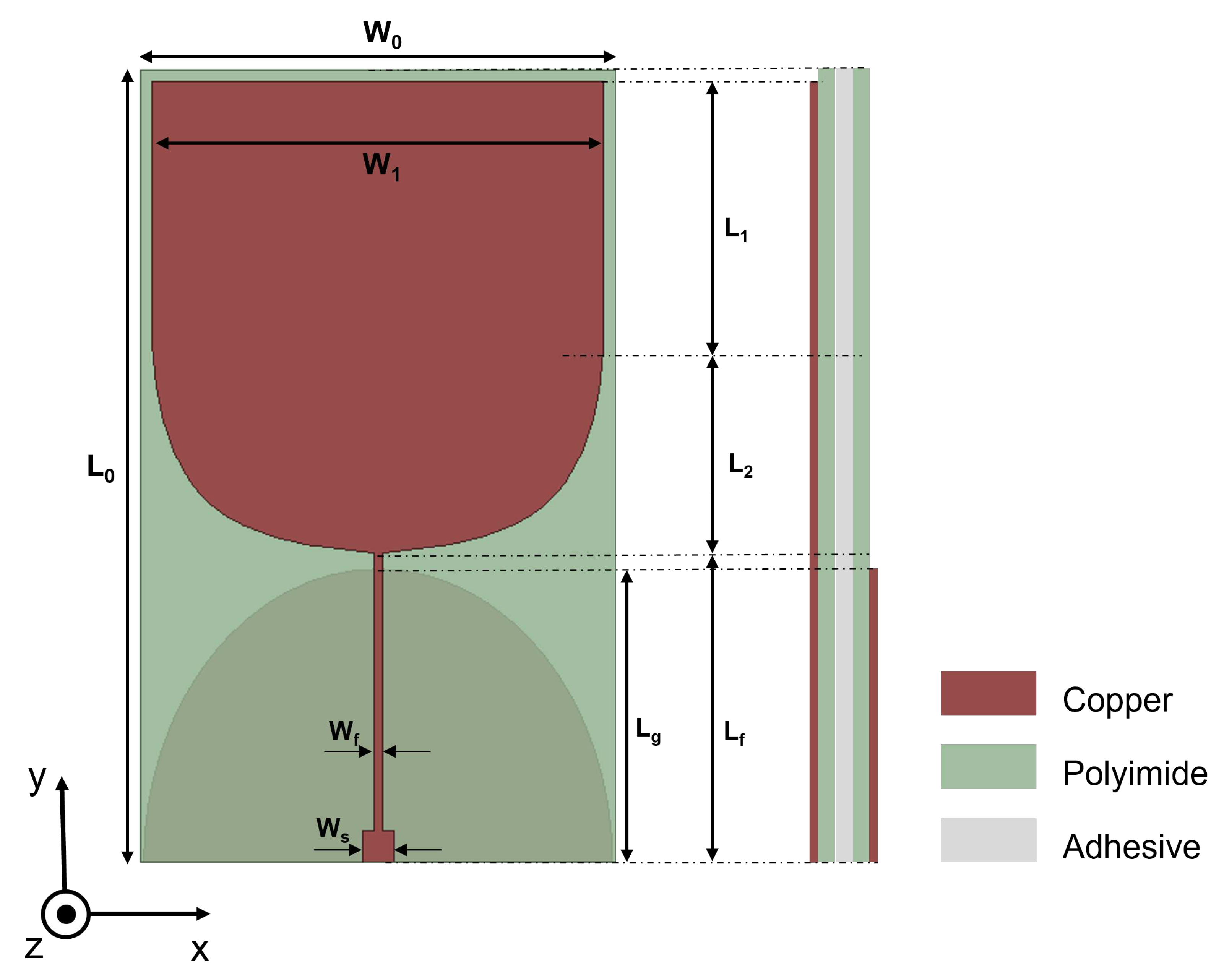
Figure 2.
Simulation results of versus frequency by varying (a), (b).
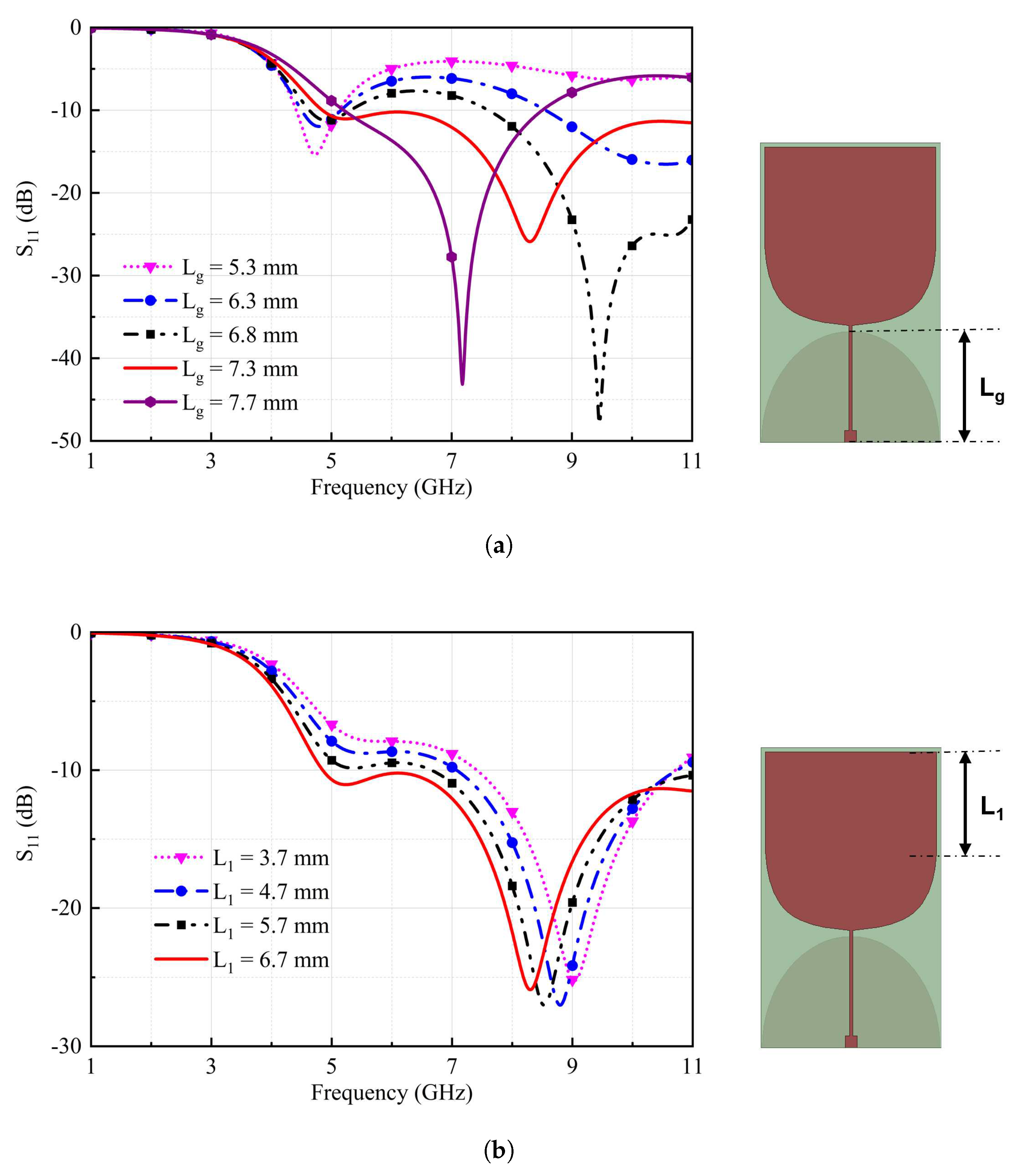
Figure 3.
Fabricated antenna prototype with an SMA connector (a) Front view, (b) Back view.
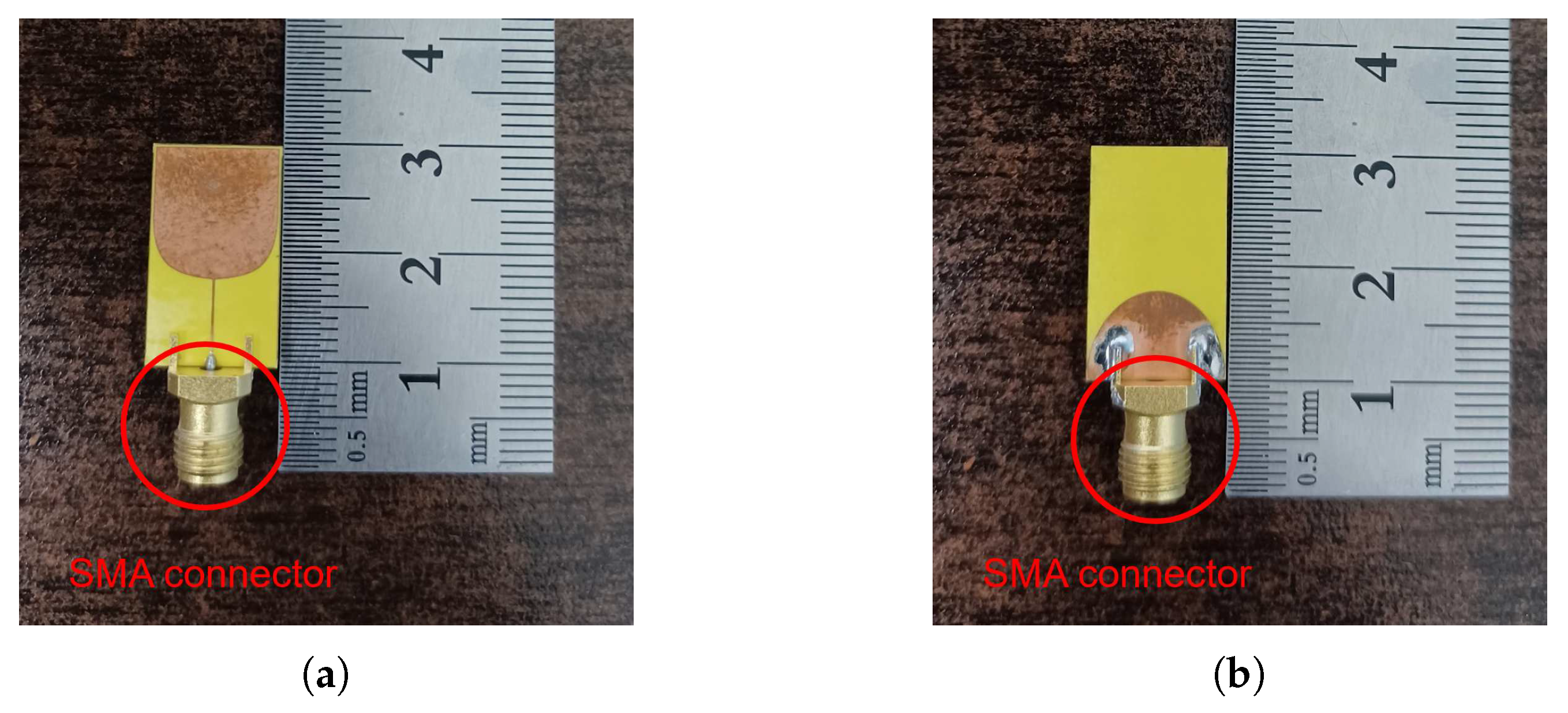
Figure 4.
Comparison of simulation and measurement results.
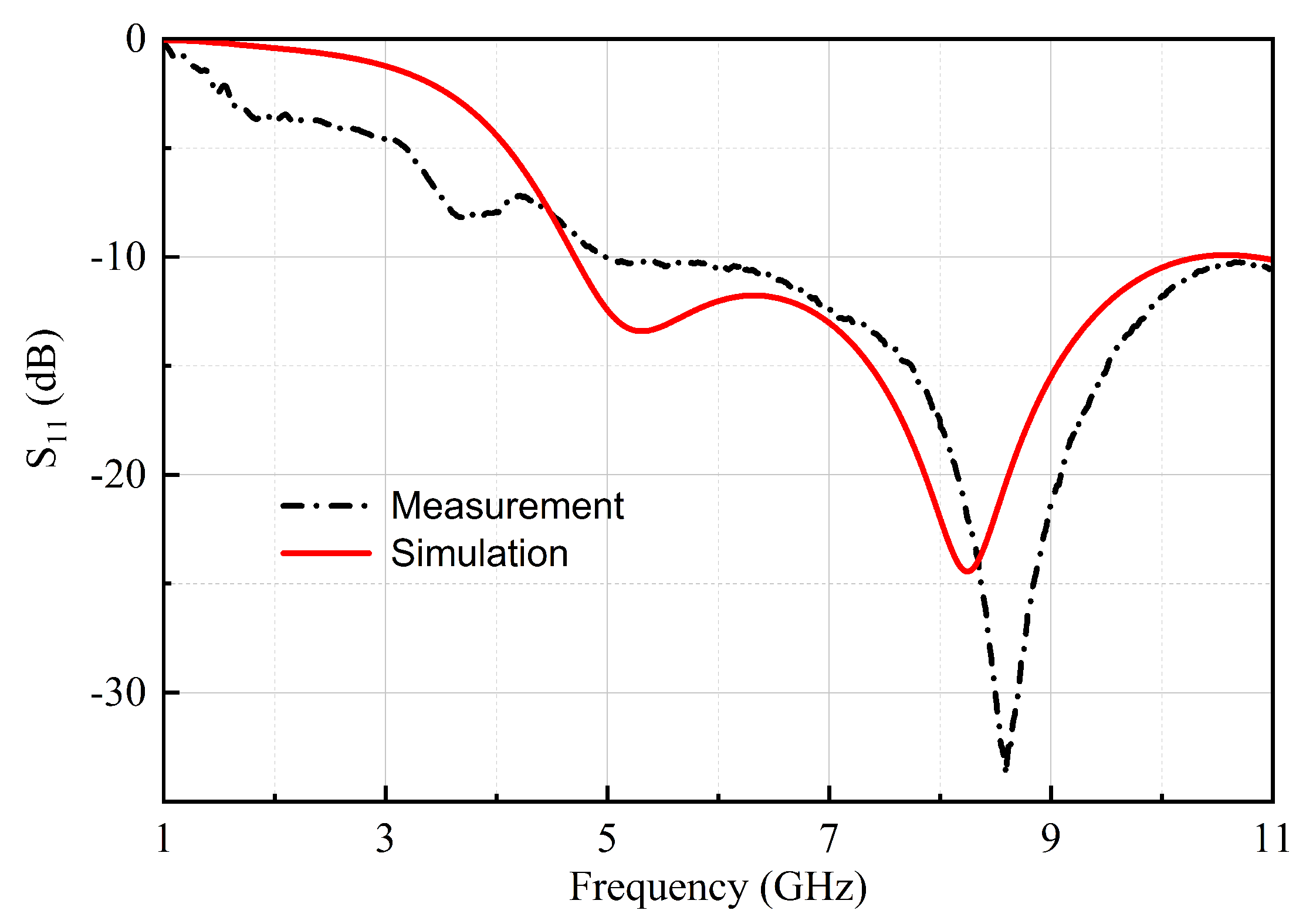
Figure 5.
The fabricated antenna located in anechoic chamber.
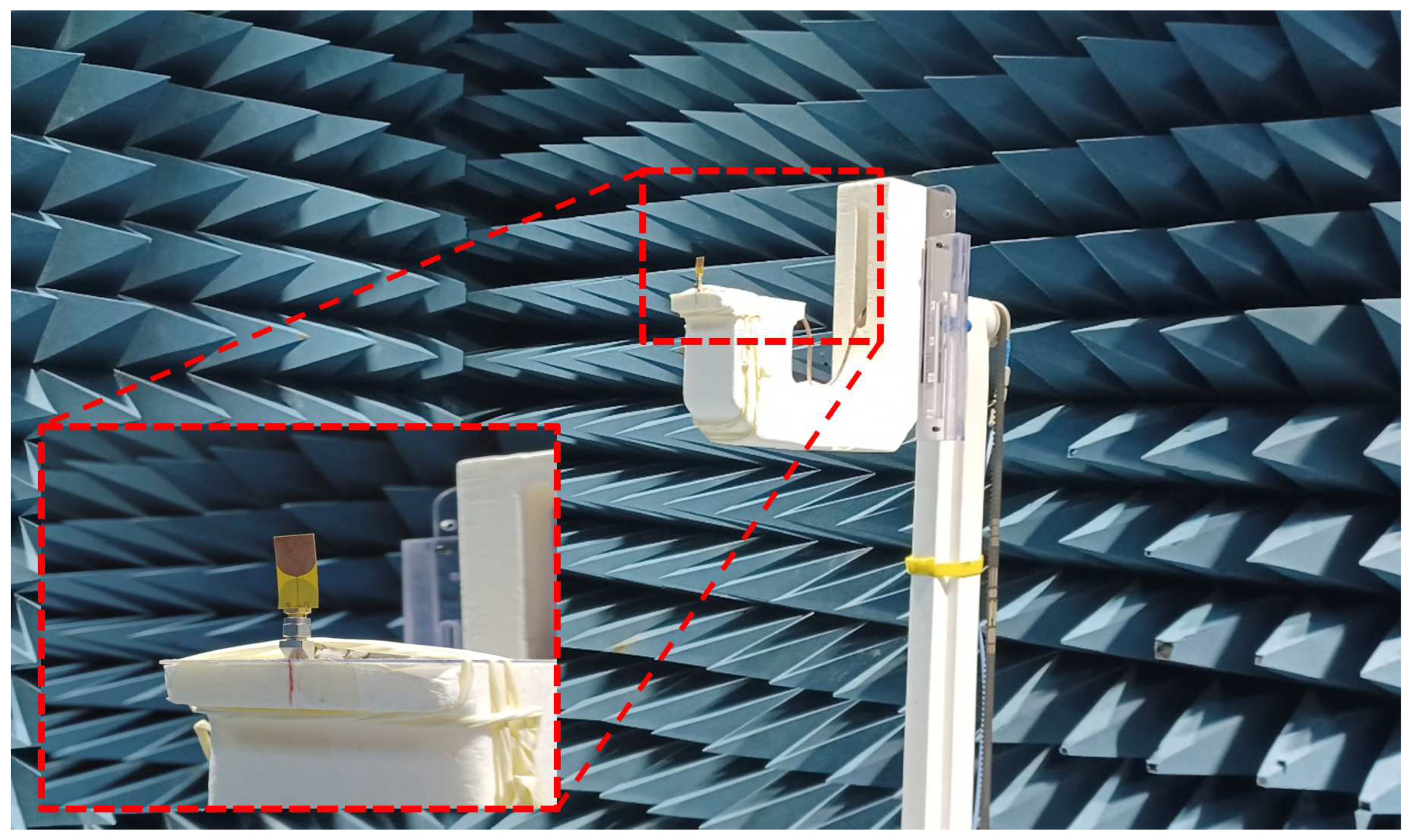
Figure 6.
Comparison of simulated and measured normalized radiation patterns at (a) 6 GHz, (b) 7.5 GHz.
Figure 6.
Comparison of simulated and measured normalized radiation patterns at (a) 6 GHz, (b) 7.5 GHz.
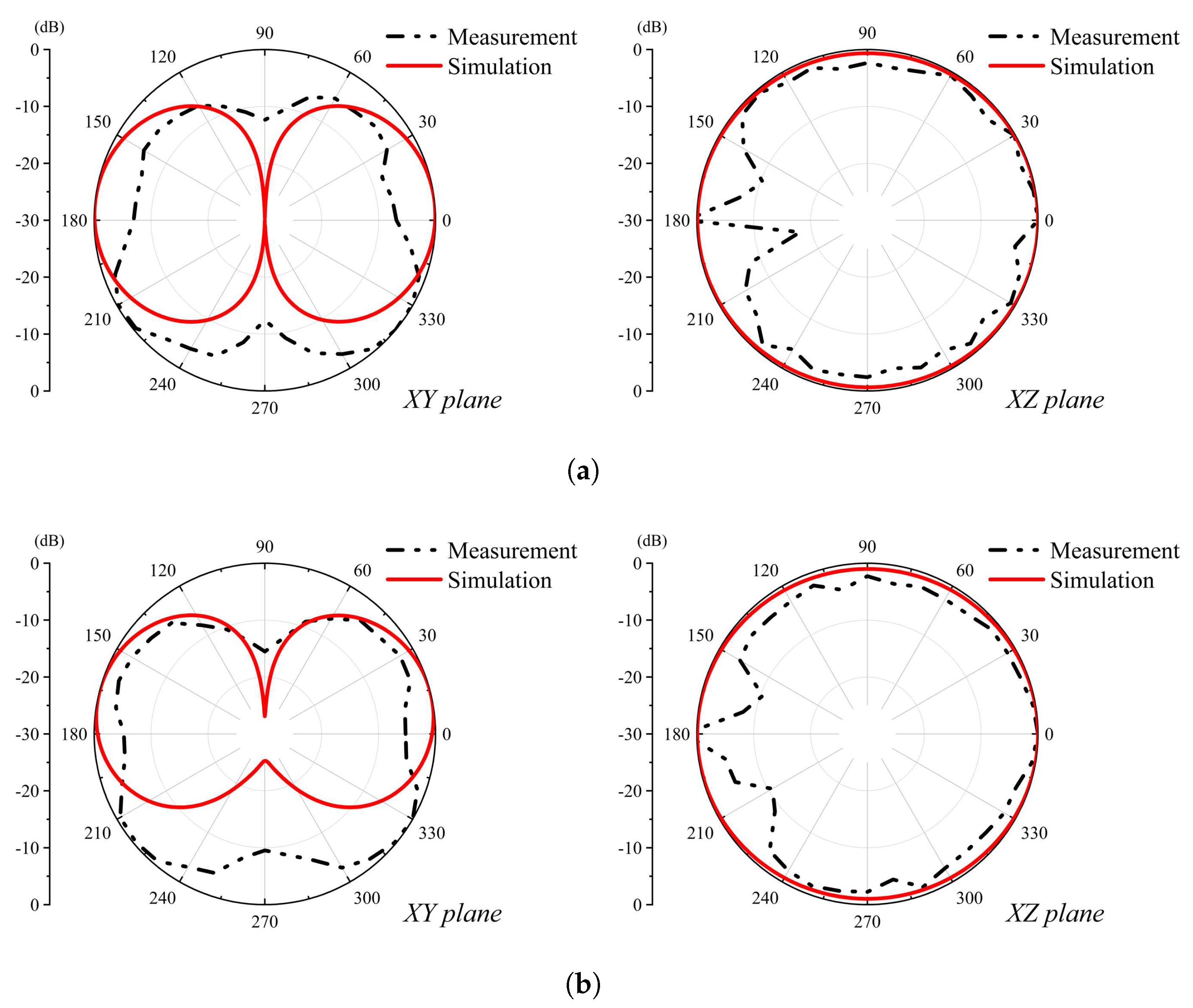
Figure 7.
Comparison of peak realized gain measurement and simulation at = 90.
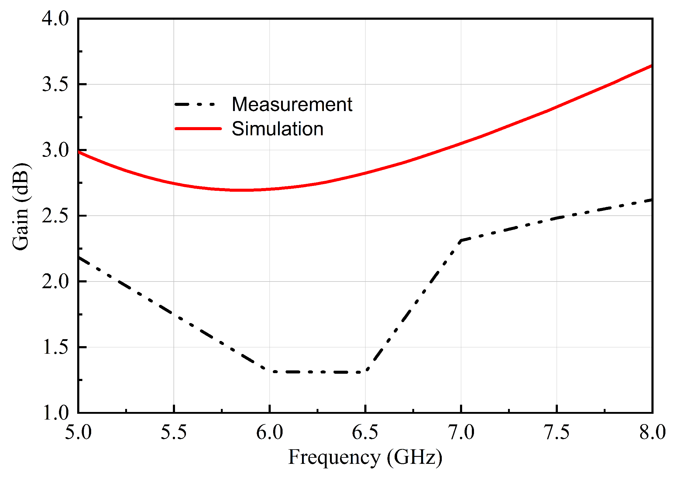
Figure 8.
Time domain measurement configurations (a) Face to face, (b) Face to side, (c) Side by side.
Figure 8.
Time domain measurement configurations (a) Face to face, (b) Face to side, (c) Side by side.
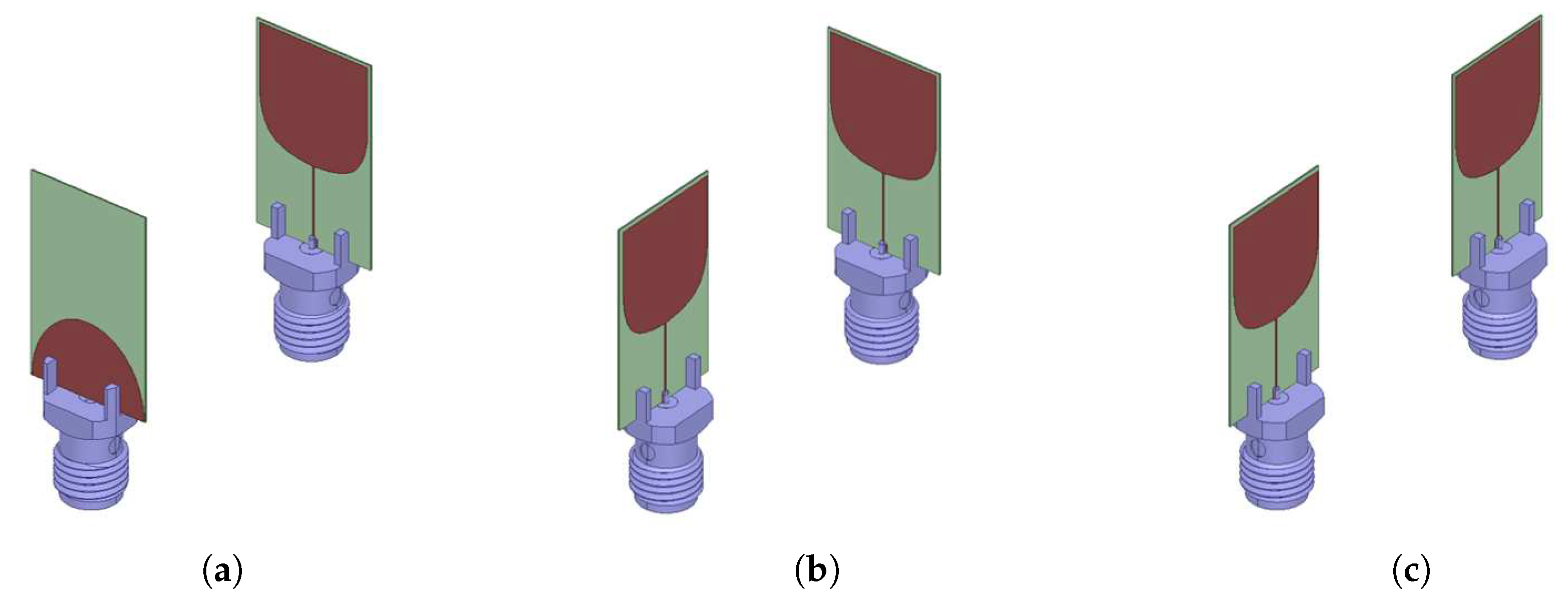
Figure 9.
Time domain measurement setup.
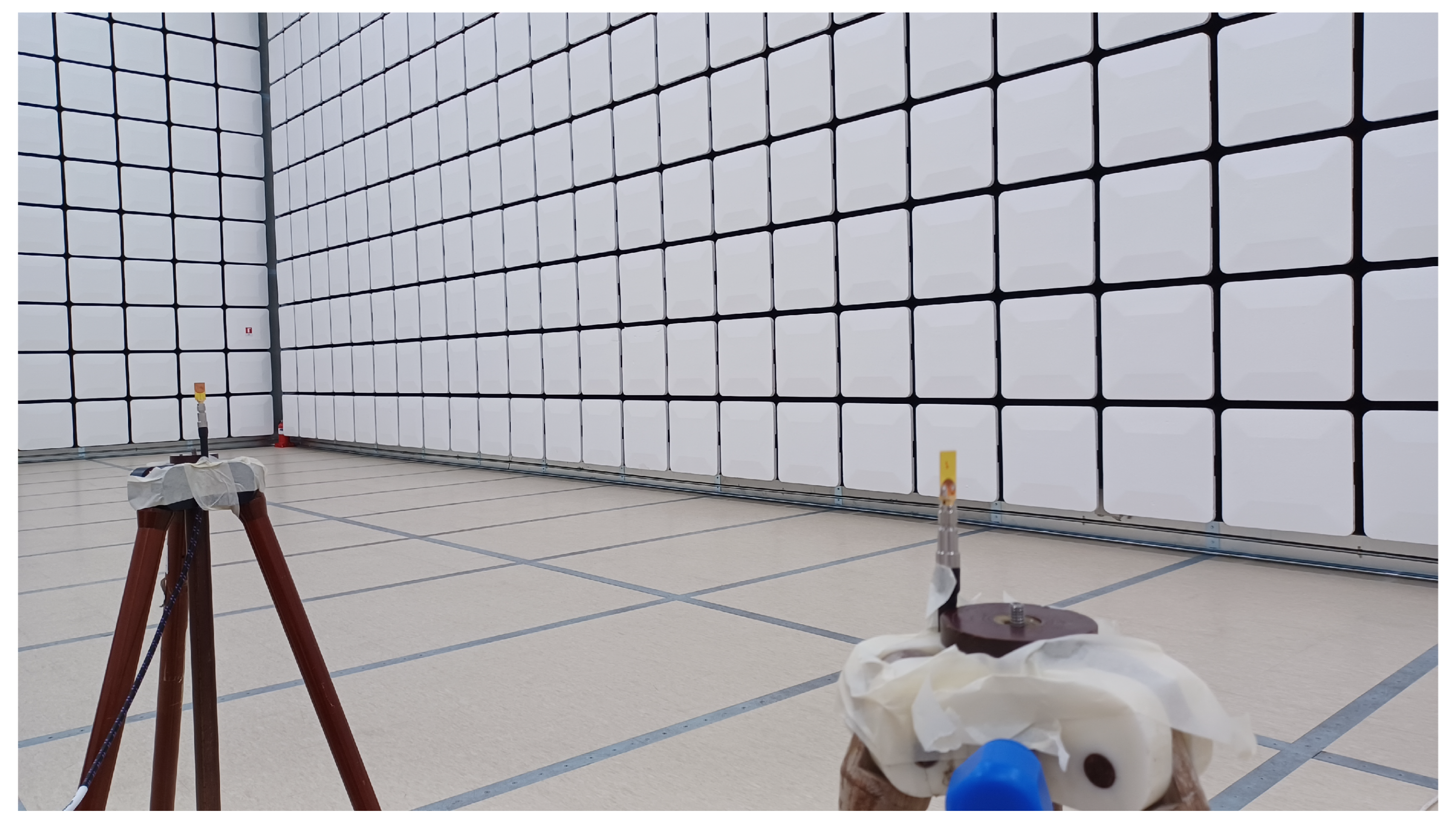
Figure 10.
Measured of three configurations.
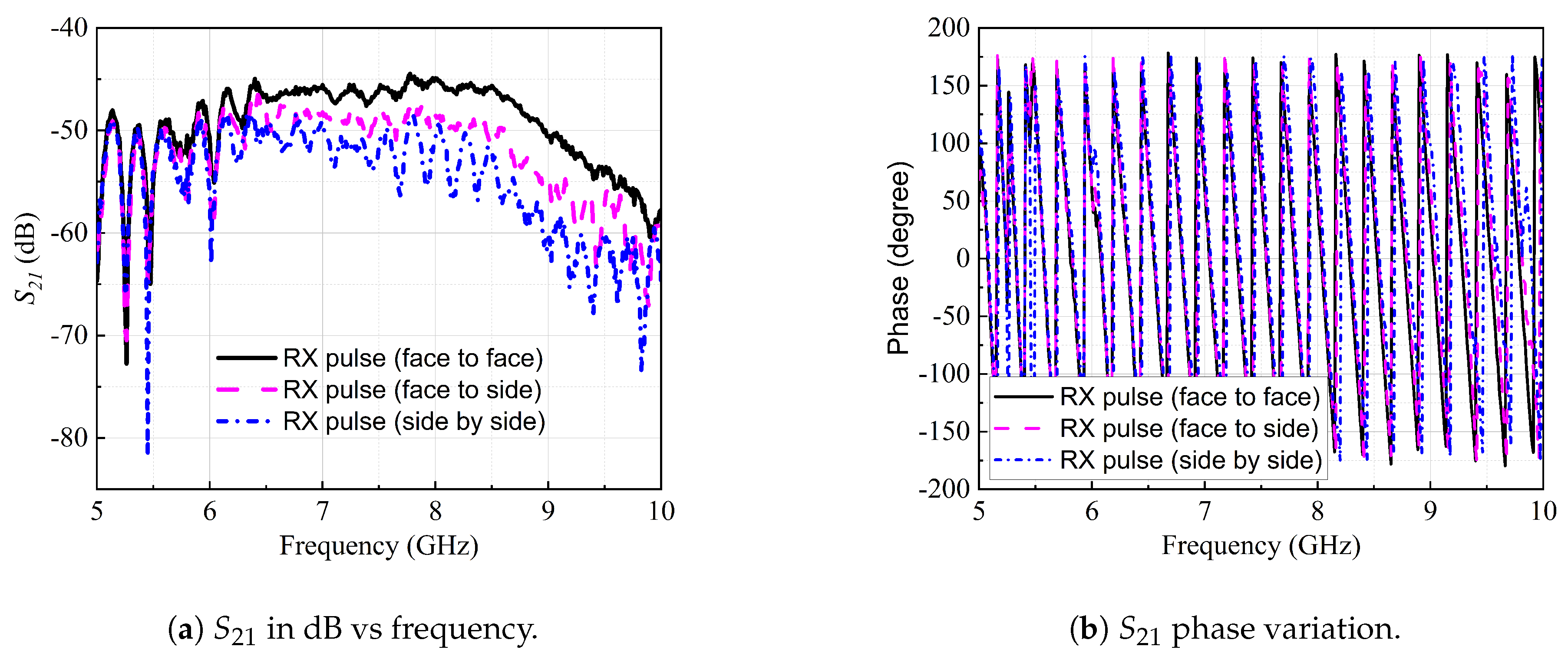
Figure 11.
Simulated input modulated SRRC pulse.
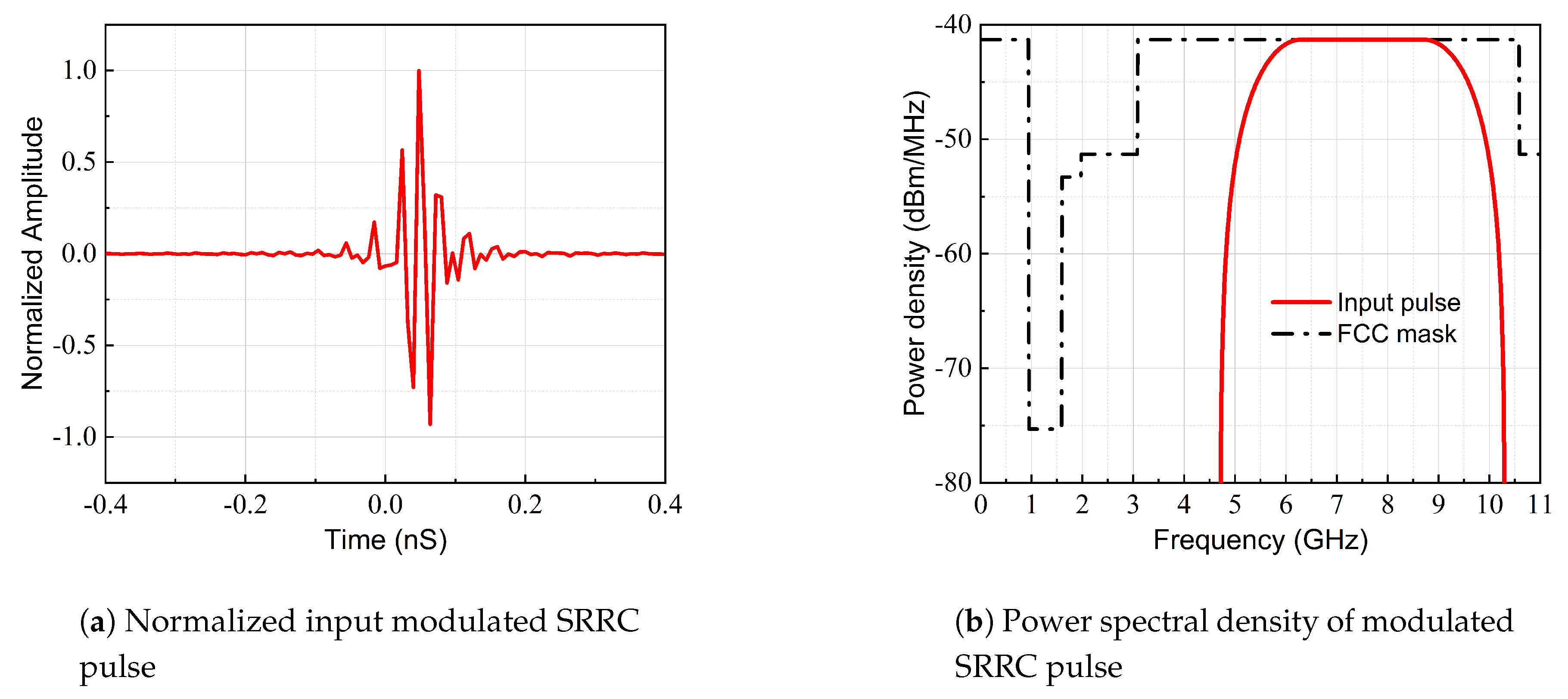
Figure 12.
Simulated normalized amplitude of input and received signal pulse.
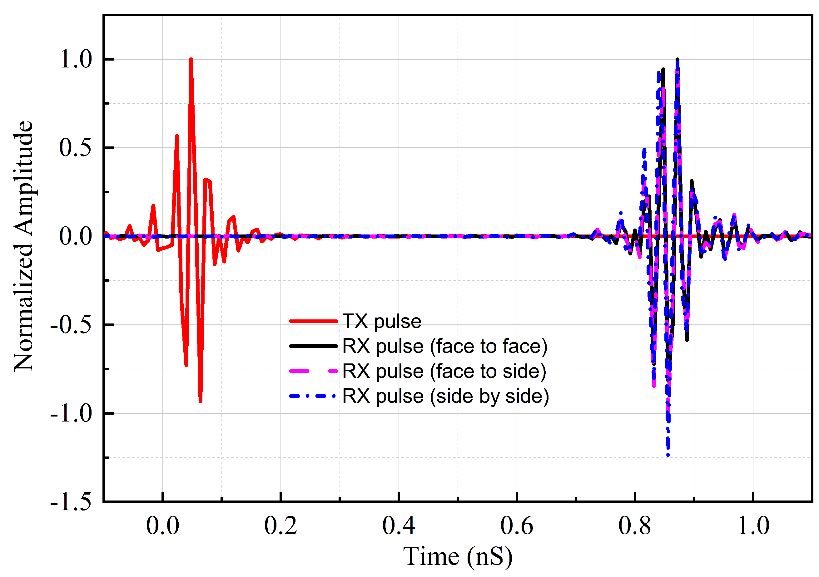
Figure 13.
Measured group delay of three configurations.
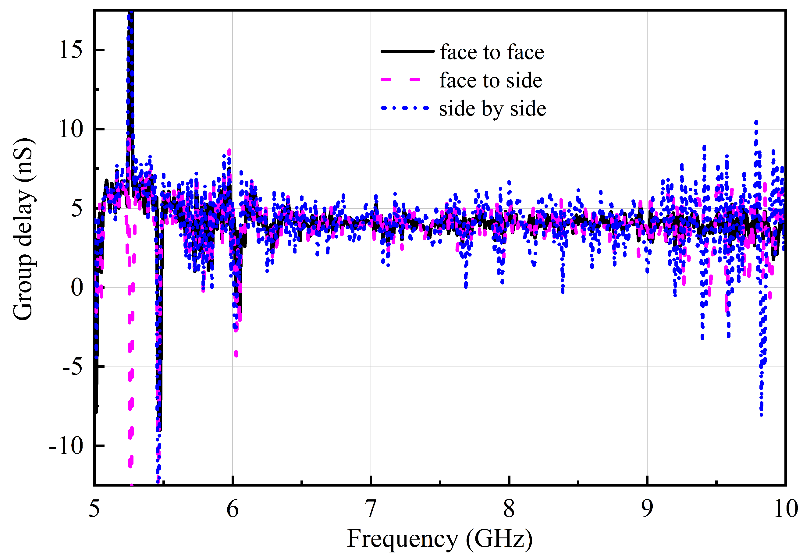

Table 1.
Optimized parameters of proposed high band antenna.
| Symbol | Value | Symbol | Value |
|---|---|---|---|
| 12.0 mm | 7.8 mm | ||
| 20.0 mm | 0.2 mm | ||
| 11.4 mm | 7.4 mm | ||
| 6.7 mm | 0.8 mm | ||
| 5.2 mm | 1.25 |
Table 2.
Fidelity factor of three configurations.
| Face to face | Face to side | Side by side | |
|---|---|---|---|
| Fidelity factor | 0.904 | 0.919 | 0.853 |
Table 3.
Comparison of various existing flexible antennas with the proposed antenna.
| Ref | Absolute size () | Electrical size () | Operating frequency (GHz) | Max gain (dB) |
|---|---|---|---|---|
| [30] | 5 - 14 | N/A | ||
| [31] | 3 - 11.2 | 1.5 | ||
| [32] | 5.2 - 6.86 | 2.94 | ||
| [33] | 3.8 – 4.5 | 3.1 | ||
| [34] | 5.5 – 7 | N/A | ||
| [35] | 2.94 - 11.17 | 3.6 | ||
| [36] | 3.04 - 10.7 | N/A | ||
| [37] | 4 - 8 | 4.1 | ||
| This work | 20 × 12 × 0.174 | 0.33 × 0.2 × 0.0025 | 5 - 10.8 | 2.9 |
Disclaimer/Publisher’s Note: The statements, opinions and data contained in all publications are solely those of the individual author(s) and contributor(s) and not of MDPI and/or the editor(s). MDPI and/or the editor(s) disclaim responsibility for any injury to people or property resulting from any ideas, methods, instructions or products referred to in the content. |
© 2020 by the authors. Licensee MDPI, Basel, Switzerland. This article is an open access article distributed under the terms and conditions of the Creative Commons Attribution (CC BY) license (https://creativecommons.org/licenses/by/4.0/).
Copyright: This open access article is published under a Creative Commons CC BY 4.0 license, which permit the free download, distribution, and reuse, provided that the author and preprint are cited in any reuse.


