
Submitted:
17 July 2023
Posted:
18 July 2023
You are already at the latest version
Abstract
The decreasing width, increasing aspect ratio RDL presents significant challenges to design for reliability (DFR) of advanced package. Therefore, this paper proposes a ML based RDL modeling and simulation method. In the method, RDL is divided into blocks and subdivided into pixels of metal percentage, and the RDL is digitalized as tensors. Then, an ANN-based surrogate model is built and trained by a subset of tensors to predict the equivalent material properties of each block. Lastly, all blocks are transformed into elements for simulations. For validation, line bending simulations were conducted on an RDL, with the reaction force as accuracy indicator. The results show that neglecting layout impact causes critical errors as substrate thins. By the method, the reaction force error is 2.81% and the layout impact can accurately be considered with 200×200 elements. For application, the TCT maximum temperature state simulation was conducted on a CPU chip. The simulation indicates that for advanced package the maximum stress more likely occurs in RDL rather than bumps, both RDL and bumps are critical impacted by layouts, and RDL stress is also impacted by vias/bumps. The proposed method precisely concerns layout impacts with little resources, presents an opportunity of efficiency improvement.
Keywords:
Redistribution layer
; layout impact
; machine learning
; thermo-mechanical simulation
; equivalent material properties
1. Introduction
Redistribution layer (RDL) is one of the most important components of the advanced packages like Chip on Wafer on Substrate (CoWoS) [1], Foveros [2], X-Cube [3], System on Integrated Chips (SoIC) [4,5], especially the multilayer RDL interposer based CoWoS-R [6], FO-PLP [7] and chiplet-based architectures [8,9]. To enable high-bandwidth signal processing between chiplets [10], several techniques such as dual damascene processing, semi-additive processing (SAP) and polymer damascene processing have been introduced. These techniques narrow the RDL trace width/pitch to as small as 2 microns [11,12] and even sub-micron [13]. To enhance the electricity transmission capacity, traces become thicker, with an aspect ratio of up to 4.2 [14], which is very different from traditional shell-like thin traces. Furthermore, wafer level integrations can stack up to 5 metal layers [1], with the area up to 1200mm2 [15], or even as extensive as 2500mm2 [1]. As a result, RDLs in advanced packages become extremely complex in shape and behavior, posing great challenges in accurately capturing its thermo-mechanical characteristics. Additionally, in advanced packages as substrate is extremely thinned to several microns or even sub-micron [16] which is similar to or even thinner than RDL, making the RDLs more prominent comparing to other package components [17,18]. For this reason, RDLs are playing crucial roles in package thermo-mechanical characteristics.
Integrated packages face severe thermo-mechanical risk due to the coefficient of thermal expansion (CTE) mismatch between materials, the accelerated thermal cycling test (TCT) [19] is an important approach for assessing their reliability. As a low-cost alternative of testing, finite element analysis (FEA) simulation under TCT conditions becomes a significant research area on design for reliability (DFR). Balancing between efficiency and accuracy of simulation is a critical issue in this field.
For traditional integrations, due to the thicker substrate and larger trace width/pitch, axisymmetric FEA model can meet the efficiency and accuracy requirements for DFR. By 2D axisymmetric model, Lee et al. [20], Che et al. [21], Machani et al. [22] simplified the RDLs into homogeneous rectangles and refined the outermost bump, then evaluated the fatigue life of the bump through transient simulation. By 3D axisymmetric model, Lee et al. [23], Che et al. [24] simplified the RDL into homogeneous films and refined the corner solder, thus assessed the reliability of stacked-chip packages. However, advanced packaging has different structural characteristics.
For advanced packages, RDL plays a more significant role in thermo-mechanical reliability. Therefore, more precise RDL modeling approaches are required for DFR of advanced packages. Dividing the RDL then employing material equivalization is a widely used strategy to improve the accuracy. In this strategy, division size and equivalization method are crucial for efficiency and accuracy. When efficiency is concerned, RDL will be divided into large size regions, and there are three typical material equivalization methods. The first method, employed by Wang et al. [25], involves calculating the isotropic materials based on the copper ratio within each region. The second method, used by McCaslin et al. [26], is determining the anisotropic equivalent material properties of regions consisting of simple shape traces through composite material mechanics. The third one, utilized by Valdevit et al. [27], is the morphology-based approach, where regions are categorized into 'lines', 'vias', or 'web' types, then specific mathematical models are developed to compute the material properties for each type of region. When accuracy is concerned, RDL will be divided into small size blocks, and there are also three typical material equivalization methods. The first method, employed by Lien et al. [28], involves calculating the isotropic equivalent material properties based on the metal percentage within each block. The second method, used by Lee et al. [29], focuses on calculating the anisotropic material properties and the equivalent reference temperature of blocks using composite material mechanics. The third one, introduced by Gibson [30], and Lee et al. [29], is a simulation-based approach that calculates the anisotropic equivalent material properties of blocks containing complex traces. To achieve higher accuracy, Yaddanapudi [31] divided the RDL into extremely small size pixels and directly defined each pixel as either metal or dielectric, a high-fidelity structural response of RDL was achieved by consuming large amount of solving resources. In general, existing work indicates that there is a trade-off between division sizes and the material equivalization method. The key to balancing efficiency and accurately lies in obtaining the anisotropic equivalent material properties quickly and accurately under larger division size.
Recently, machine learning (ML) has shown the capability of extracting interpretable models from scientific data automatically [32], and it has been increasingly employed in the material equivalization of composite materials in 3D and 2D structures. Regarding 3D, Dai et al. [33] used feature matrixes to digitally represent the lattices orientations of 3D structures, and then created a graph-Artificial Neural Network (ANN) to predict the structural performance. Regarding 2D, Liu et al. [34], Ye et al. [35] and Gong et al. [36] used high-resolution grayscale matrix to digitalize the planar strictures, then constructed convolutional neural networks (CNNs) to quickly predict the equivalent mechanical properties. Due to the accurate and fast predictive capabilities of models created based on ML, it has been introduced into the modeling and simulation of integrated package. For example, Selvanayagam et al. [37,38] partitioned an 8-RDLs interposer into 3×3 regions, then established surrogate models that link the copper ratio in each layer within each region to the warpage in TCT condition, then ultimately optimized the global package warpage.
In this work, we applied ML for material equivalization and developed a RDL modeling and simulation method for DFR of advanced packages. In this method, a RDL is divided into equal-size blocks. To describe the layout within each block, we further subdivided each block into pixels and represent each pixel using the metal percentage. Consequently, each block can be represented as a tensor composed of pixel metal percentages, and the entire RDL is digitalized as the collection of such block tensor. An ANN is constructed using either fully connected neural networks (FCNN) or convolutional neural networks (CNN), to model the relationship between the block tensor and the corresponding equivalent material properties. Subsequently, the ANN is trained by a small subset of tensors with the equivalent material properties obtained through finite element analysis (FEA) as labels, then the material surrogate model is constructed. Lastly, all blocks are transformed into FEA elements and assigned the material properties predicted by the model, then completing the modeling and simulations of the RDL.
To validate the efficiency and accuracy of the proposed method, line bending simulations were conducted for a 21.6×21.6mm² RDL. The detailed fine mesh model served as the benchmark, with the reaction force being regarded as the accuracy indicator. The results show that as the reduces of substrate thickness, the reaction force error of the traditional method that neglects layout impact increases sharply, indicating that critical layout impact must be considered in the simulation of advanced package. When the proposed method is used with a substrate thickness of 50μm, the reaction force error is 2.81% the layout impact can accurately be estimated utilizing only 200×200 elements, the number of elements is only 1/15 of the traditional approach.
As an application case, a simulation was introduced to investigate the thermo-mechanical response of a 2.5D integrated CPU chip at the maximum temperature state in TCT. The results indicate that for advanced packages the maximum stress more likely to occur in the RDL, which is different from the traditional integrations where the maximum stress occurs in the bumps. It also reveals that the stress of both the RDL and bumps are significantly impacted by the layout. Moreover, it is observed that the stress in RDL is particularly impacted by vias and bumps in adjacent layers.
The method precisely concerns these layout-related impacts with minimal resources and time, presents an opportunity to improve the efficiency of advanced package DFR.
2. Methods
The general workflow of the proposed modeling method is shown in Figure 1 and consists of the following steps:
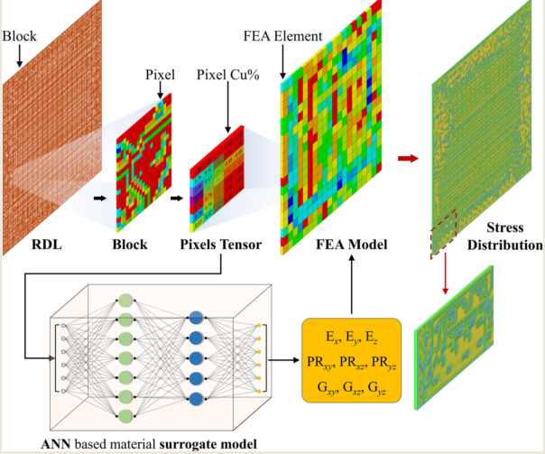
Step 1: Two-level RDL digitalization, this step is consisted by global and local discretization. In the global level, the package level RDL pattern is divided into equal-size RDL blocks containing a part of traces, and there are Qx blocks along the X direction and Qy along Y. To capture the layout feature within block, in the local level, each RDL block is divided into pixels with uniform size. The subdivision results in PQx pixels along the X direction and PQy pixels along Y, the pixel value is defined as the metal percentage within pixel region. Consequently, the RDL block can be represented by a PQx×PQy tensor, and the package-level RDL can be digital represented by Qx×Qy tensors.
Step 2: ANN Training dataset preparing, this step prepares the ANN training dataset by randomly selected a small subset of RDL blocks. The dataset consists of input tensors and labels representing the anisotropic equivalent material properties of each block obtained through 3D FEA simulations [16], including Young's modules, Poisson's ratios, shear modules, thermal conductivities and CTEs in all directions.
Step 3: ANN-based surrogate model establishing, this step establishes an ANN-based material surrogate model. The input data of the surrogate model is the RDL block tensor and the output data include all equivalent properties. The surrogate model employs ANN and is trained by the dataset prepared in Step 2. Once established, the ANN eliminates the need for repeating Steps 2 and 3, it would be highly advantageous for the repeated design iteration process.
Step 4: Equivalent properties predicting, all equivalent properties for all the RDL blocks generated in Step 1 are predicted by the surrogate model established in Steps 2, 3.
Step 5: Global FEA model building, all RDL blocks are transformed into 3D hexahedral solid elements to construct the global RDL FEA model and assigned the material properties predicted by Step 4. The model consists of Qx×Qy elements encompassing the entire RDL, and can also serve as a part of the package-level FEA model.
As the method implementation, a series of programs are established, including: the ANN implemented by Pytorch, the main framework developed in Python and the FEA simulator powered by ANSYS 18.2. The RDL blocks creating processes are implemented by C++. In addition, the C# developed program is used as the graphical post-processor.
2.1. ANN Architectures
Activation function, rectified linear unit (ReLU) is selected as the activation function, shown by (1), (2):
Loss Function, cross-entropy loss is selected as the loss function, shown by (3):
Where, n is the number of samples, yi represents the true value of the i-th sample, represents the predicted value of the i-th sample, wi represents the weight of the i-th sample. The loss for a batch prediction, shown by (4):
Where, batch is the number of predicting procedures for one predicting batch. For the j-th predicting procedure of the batch, yij represents the true value of the i-th sample, represents the predicted value of the i-th sample and wi represents the weight of the i-th sample.
Optimizer, the stochastic gradient descent (SGD) is adopted to optimize neural network, and momentum is considered during the optimization process. Learning rate and momentum parameters are adjusted to fine-tune the optimization process, as indicated in equations (5) and (6)
Where, t is the current iteration step number, relatively t–1 is the number of the previous step, lr represents the learning rate, g is the gradient, m means the momentum. vt, wt represents the velocity and weight in current iteration step respectively. vt-1, wt-1 represents the velocity and weight in the previous step respectively.
ANN networks, full-connected neural network (FCNN) and convolution neural network (CNN) are created. As shown in Figure 2, the FCNN includes an input layer, output layer and several hidden layers. The parameters of the input layer are represented by the vector shown by (7) and the size of the input vector shown by (8):
where, is the metal percentage of the p-th pixel, Qin is the vector size which is equal to the number of pixels of a single RDL block, PQx and PQy represent the number of RDL block’s pixels along the X and Y direction respectively. The output vector of the FCNN includes all 15 anisotropic equivalent material properties of the RDL block, shown by (9):
The hidden layer can be represented by vector as (10):
where, is the value of the i-th node, Qn is the number of nodes of the n-th hidden layer.
Shown as Figure 3, the CNN is consisted by convolution network and the full-connected network, the input parameters are the tensor with size of [PQx, PQy, 1], and the output vector is the same as (7). The convolution network contains convo lution layers and max pooling layers and the tensor is transf ormed through layers. The tensor size is [Cnx, Cny, Cnz] after the n-th convo lution layer, and [Pnx, Pny, Pnz] after the n-th max pooling layer. The output tensor of the convolution network can be compressed into the vector of size QLin.
where, Pnx, Pny, Pnz are the output tensor size in X, Y and Z directions respectively.
2.2. Training dataset augmentation
To augment the training dataset of blocks, the geometric symmetry and data transformations are employed. The initial block with anisotropic properties (Ex = Ex0, Ey = Ey0) is shown in Figure 4a, and it can be rotated by 90°, 180°, and 270°, as indicated in Figure 4b,d, respectively. When the angle of rotation is 90° or 270°, the anisotropic properties are transformed to Ex = Ey0, Ey = Ex0. The initial block and its rotated versions can also be flipped in the Y direction, as shown in Figure 4e–h, while keeping the same anisotropic properties. Eight unique blocks can be generated from the initial one, without requiring additional FEA solutions.
3. Result and discussions
3.1. Method validation
The two-layer model containing RDL and a silicon substrate is shown in Figure 5 is established for validation. The model consists of the substrate layer and the RDL (the M1 layer), the materials involved in the simulations are listed in Table 1, and all materials are assumed to be linear elastic. The substrate is made up of Si, its thickness (TB) is set as a variable parameter, with a range of values from 20μm to 500μm. The RDL is consisted by Cu and PI, the thickness (TR) is 10μm. The layout pattern of M1 layer is shown in Figure 6 and the domain direction of traces is the X direction.
The validation of the adaptability to the mechanical loads is based on the parallel trace bending load case (CaseP) and vertical trace bending load case (CaseV) shown in Figure 5. In the CaseP, nodes on X = 0 face are constrained in the X, Y and Z directions, nodes on the top line of X = Length face are set Z = -0.5 mm. In the CaseV, the constrain are set on Y = 0 face, and the displacement load are set on the top line of Y = Width face.
As the benchmark, a detailed RDL fine mesh model consisting of 640,365 nodes and 606,482 elements was established with a substrate thickness of 50μm. The solving process cost 176s. The stress distributions are depicted in Figure 7, stress concentrations can be observed at discontinue positions, indicating the critical impact from layout.
The sums of the Z-direction reaction forces of all nodes applied displacement loads in CaseP and CaseV are FRDP: -7.174E-03N and FRDV: -6.464E-03N, respectively. The reaction force errors serve as accuracy indicators, as shown in (12).
Where, ErrorP and ErrorV are reaction force errors for CaseP and CaseV respectively. FRP and FRV are reaction force to be evaluated for CaseP and CaseV, respectively.
For the proposed method, considering the efficiency and accuracy set the global mesh divisions: Qx = Qy = Q = 200, the local pixel division: PQx = PQy = PQ = 15 and built 40,000 RDL blocks. Qt blocks are randomly selected as the ANN training dataset, the default value of Qt is 1000, and the testing dataset contains all the 40,000 blocks. A FCNN with two hidden layers is employed for the ML based method. As depicted in Figure 2, the first hidden layer contains 400 nodes (H1 = 400), while the second one has 300 nodes (H2 = 300). Set the learning rate: lr = 0.02, the momentum: m = 0.5, the training epoch: q = 250. The training and testing processes are run using a GPU of NVidia RTX 3070Ti, the average predicting time of all blocks are 3.652 s, and the loss variation is shown by Figure 8.
The calculated material properties shown in Figure 9 indicate the ML-based method predicted material properties are very close to those obtained by the simulation-based method, which demonstrates the accuracy of the ANN-based surrogate model. Additionally, notable difference between Young’s modulus along the trace direction (Ex) and perpendicular (Ey). Moreover, reduction in Ey is obvious within the gap area between traces, indicating the critical impact of RDL layout on the mechanical behavior of RDL.
The stress distribution shown in Figure 10 is well consistent with the result of the detailed fine mesh model presented in Figure 7. Additionally, the reaction force errors for CaseP and CaseV are 1.72% and 2.81%, respectively, validating the precision of this method. Furthermore, the proposed approach only requires 200×200 FEA elements, whereas the detailed fine mesh model consists of 15 times more elements. This demonstrates that the approach contributes significant resource savings in simulation.
Furthermore, to verify the accuracy of thermo-mechanical simulations, parallel trace warpage case (CasePT) and vertical trace warpage case (CaseVT) are created as shown in Figure 11. Except to the 150 ℃ temperature, nodes on X = 0 and Y = 0 faces are constrained in the X, Y and Z directions in CasePT and CaseVT cases, respectively. Figure 12 and Figure 13 show the Z direction displacement and von Mises stress distributions of the cases, they present almost identical deformation and stress distributions to the detailed fine mesh model.
3.2. Key factors influence
The influence of the substrate thickness, global mesh division, training dataset size, and ANN architecture to the prediction process is investigated.
The influence of the substrate thickness.
Three simulation methods were performed, including the traditional layout neglecting block-based method, the simulation-based method and the proposed ML-based methods, on seven substrate thickness values: 20, 50, 100, 200, 300, 400, and 500μm. Figure 14 summarizes the reaction force errors of each case, demonstrating the fact that as the substrate thickness decreases, the impact of RDL layout becomes more and more critical, neglecting the layout features will result in substantial errors.
The influence of the global mesh division.
Another two global division values of 100 and 300 are conducted to investigate the influence of the global division. Figure 15 summarizes the reaction force errors of different cases, illustrating that larger global mesh divisions can improve solution accuracy, albeit at the cost of increased solving time and resource consumption.
Figure 16 depicts stress distributions at Q = 100 and Q = 300, the stress distribution shown in Figure 16a is similar to those shown in Figure 7 and Figure 10, indicating that the proposed method can accurately capture the layout impact shown in Figure 6 using only 100×100 elements. Moreover, larger Q values can capture more accurate pattern features but may not justify the increased time and resource consumption. Regarding the block-based method, as shown in Figure 17, obvious stress inhomogeneity only becomes captured until Q ≥ 600. Moreover, even when Q = 800, Figure 18 demonstrates that the accuracy cannot match the proposed method. However, simulation costs become exorbitant.
The influence of the training dataset size.
ANNs was established using ten different dataset sizes ranging from 500 to 5000. Figure 19 summarizes the loss and training time and indicates that increasing dataset size generally results in improved prediction accuracy, although the effect becomes negligible beyond 2000 data points. Furthermore, the proposed dataset augmentation algorithm can significantly enhance the prediction accuracy as shown in Figure 20.
The influence of the FCNN architectures
Three different types of FCNNs with two hidden layers and varying numbers of hidden nodes are established. The training and prediction losses are summarized in Figure 21a and show that increasing the number of hidden layer nodes results in improved prediction accuracy. However, the effect becomes less significant as the number of nodes increases. Additionally, Figure 21b illustrates the accuracy results obtained from the FCNNs with three hidden layers and varying numbers of nodes, showing that while additional layers can improve accuracy, their benefit is limited and requires more training time.
Application of the CNN architectures.
Figure 22 summarizes the losses and training time for “1 CNN + 1 FCNN”, “1 CNN + 2 FCNNs” and “2 CNNs + 2 FCNNs”. The results demonstrate that while CNNs have shorter training time, they exhibit significantly larger losses across all three architectures, indicating undesired defeaturing during convolution and pooling operations negatively impacts prediction accuracy.
3.3. Large area 2.5D integrated CPU chip thermo-mechanical simulation
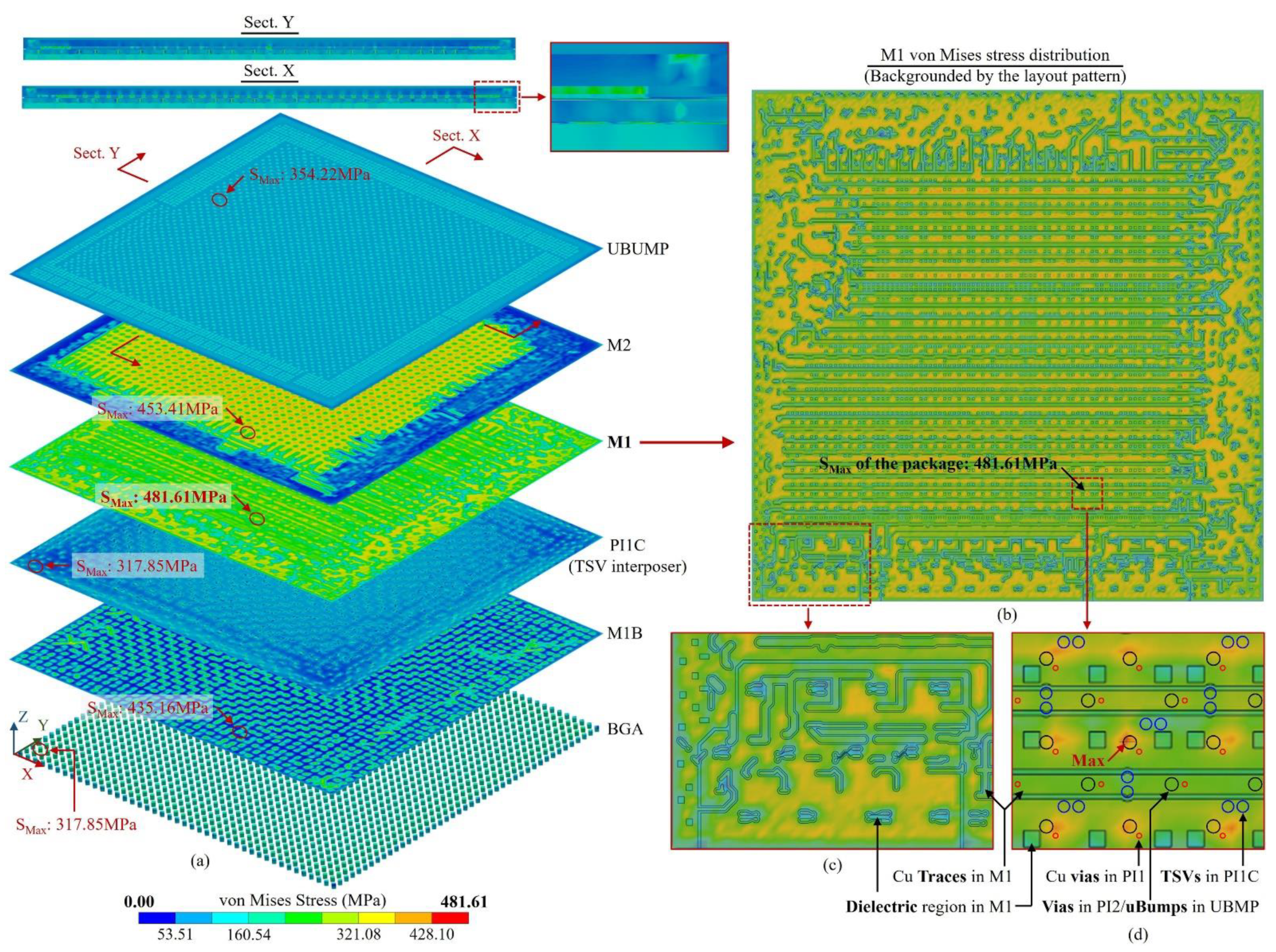
As an application, a 2.5D integrated CPU chip is constructed, as shown in Figure 23. All 3 RDLs are modeled by the proposed method, the division parameters are: Q = 200, PQ = 15. The training dataset size of Qt = 1000 is utilized without applying data augmentation. Predictions are made using FCNNs with two hidden layers consisting of 400 and 300 nodes, respectively. In the package-level FEA model, the maximum element size is 0.12mm, it contains 1,072,658 nodes and 625,648 elements.
To simulate the maximum temperature state of the TCT, a temperature load of 150℃ was applied and the bottom surface of the BGA was constrained in X, Y and Z directions, as shown in Figure 24. The results obtained under this condition is shown in Figure 25, indicating following information:
Firstly, it is found from Figure 25a that the maximum stress occurs in the M1 layer rather than bumps, this indicates that for 2.5D advanced packages, as the substrate thickness decreases and the trace width/pitch reduces, the thermo-mechanical risk of RDL becomes more significant. The conclusion for traditional integrations that the maximum risk always occurs at bumps is no longer accurate.
Secondly, Figure 25b,c demonstrate the fact that the stress distribution of RDL is critical impacted by layout, neglecting the layout impact would bring in critical errors. And the proposed method can accurately capture the impact.
Furthermore, it can also be found from Figure 25(a) that the location and magnitude of the maximum stress of bumps and TSVs are influenced by the layouts and surrounding structures, and it is different from the conventional understanding that the outermost bumps are the most vulnerable. Therefore, the impact of the vias and bumps layouts should also be considered in the simulation.
Finally, the detailed view of the maximum stress region of M1 layer in Figure 25d illustrates that the stress on RDL is not only influenced by the RDL layout but also critical impacted by the vias and bumps within adjacent layers.
4. Conclusions
This paper proposes a machine learning (ML) based RDL modeling and simulation method for DFR of 2.5D/3D advanced packages, taking the critical layout impact into consideration. In the method, RDL is divided into blocks and subdivided into pixels of metal percentage, such that the RDL can be digitalized as metal percentage tensors. Consequently, an ANN-based surrogate model is built and trained by a small subset of tensors to predict the equivalent material properties of each block. Lastly, all blocks are transformed into elements to build a FEA model for simulations. For the validation of accuracy, line bending simulations are conducted for a 21.6×21.6mm² RDL using the proposed method, where the reaction force is compared with a benchmark result obtained by detailed fine mesh simulation. The results show that through the proposed method, the reaction force error can be as low as 2.81% and the layout impact can be accurately considered with 200×200 elements, just 1/15 of the traditional approach. The results also show that if the layout impact is neglected, the reaction force error will increase sharply as the substrate thins. Therefore, the impact must be considered in advanced package simulation. As an application case, a simulation was introduced to investigate the thermo-mechanical response of a 2.5D integrated CPU chip at the maximum temperature state in TCT. The results indicate that for advanced packages the maximum stress more likely to occur in the RDL, which is different from the traditional integrations where the maximum stress occurs in the bumps. It also reveals that the stress of both the RDL and bumps are significantly impacted by the layout. Moreover, it is observed that the stress in RDL is particularly impacted by vias and bumps in adjacent layers. The proposed method precisely concerns layout impacts with little resource, presents an opportunity to improve the efficiency of advanced package DFR.
Author Contributions
Conceptualization, Xiaodong Wu. and Shenglin Ma.; methodology, Xiaodong Wu.; software, Xiaodong Wu.; validation, Xiaodong Wu., Zhizhen Wang.; investigation, Xiaodong Wu.; resources, Shenglin Ma.; writing—original draft preparation, Xiaodong Wu.; writing—review and editing, Xiaodong Wu., Shenglin Ma. and Zhizhen Wang., Xianglong Chu., Chunlei Li., Wei Wang., Yufeng Jin.; visualization, Xiaodong Wu.; project administration, Shenglin Ma. All authors have read and agreed to the published version of the manuscript.
Funding
This research received no external funding.
Conflicts of Interest
The authors declare no conflict of interest.
References
- Huang, P.K.; Lu, C.Y.; Wei, W.H.; Chiu, C.; Ting, K.C.; Hu, C.; Tsai, C.H.; Hou, S.Y.; Chiou, W.C.; Wang, C.T.; et al. Wafer Level System Integration of the Fifth Generation CoWoS®-S with High Performance Si Interposer at 2500 Mm2. In Proceedings of the 2021 IEEE 71st Electronic Components and Technology Conference (ECTC); IEEE, San Diego, CA, USA, June 2021; pp. 101–104. [Google Scholar]
- Ingerly, D.B.; Enamul, K.; Gomes, W.; Jones, D.; Kolluru, K.C.; Kandas, A.; Kim, G.-S.; Ma, H.; Pantuso, D.; Petersburg, C.F.; et al. Foveros: 3D Integration and the Use of Face-to-Face Chip Stacking for Logic Devices. In Proceedings of the 2019 IEEE International Electron Devices Meeting (IEDM); IEEE, San Francisco, CA, USA, December 2019; pp. 19.6.1–19.6.4. [Google Scholar]
- SAMSUNG, X-Cube technology. Available online: https://semiconductor.samsung.com/us/foundry/advanced-package/ (accessed on 28 June 2023).
- Yu, D.C.H.; Wang, C.-T.; Lin, C.-C.; Lu, C.-H.; Wu, G.; Huang, C.-Y.; Chen, W.-T.; Ku, T.; Yee, K.-C.; Tsai, C.-H. SoIC_H Technology for Heterogeneous System Integration. IEEE Trans. Electron Devices 2022, 69, 7167–7172. [Google Scholar] [CrossRef]
- TSMC-SoIC. Available online: https://3dfabric.tsmc.com/english/dedicatedFoundry/technology/SoIC.htm#SoIC_CoW (accessed on 28 June 2023).
- Lin, M.L.; Liu, M.S.; Chen, H.W.; Chen, S.M.; Yew, M.C.; Chen, C.S.; Jeng, S.-P. Organic Interposer CoWoS-R + (plus) Technology. In Proceedings of the 2022 IEEE 72nd Electronic Components and Technology Conference (ECTC); IEEE, San Diego, CA, USA, May 2022; pp. 1–6. [Google Scholar]
- Kim, H.; Co, S.E. Advanced Fan-Out Panel Level Package (FO-PLP) Development for High-End Mobile Application.
- Ahmad, M.; DeLaCruz, J.; Ramamurthy, A. Heterogeneous Integration of Chiplets: Cost and Yield Tradeoff Analysis. In Proceedings of the 2022 23rd International Conference on Thermal, Mechanical and Multi-Physics Simulation and Experiments in Microelectronics and Microsystems (EuroSimE); IEEE, St Julian, Malta, 25 April 2022; pp. 1–9. [Google Scholar]
- Suggs, D.; Subramony, M.; Bouvier, D. The AMD “Zen 2” Processor. IEEE Micro 2020, 40, 45–52. [Google Scholar] [CrossRef]
- High Bandwidth memory (HBM) DRAM. Available online: https://www.jedec.org/standards-documents/docs/jesd235a (accessed on 28 June 2023).
- Kudo, H.; Takano, T.; Tanaka, M.; Mawatari, H.; Kitayama, D.; Tai, T.; Tsunoda, T.; Kuramochi, S. Panel-Based Large-Scale RDL Interposer Fabricated Using 2-Μm-Pitch Semi-Additive Process for Chiplet-Based Integration. In Proceedings of the 2022 IEEE 72nd Electronic Components and Technology Conference (ECTC); IEEE, San Diego, CA, USA, May 2022; pp. 836–844. [Google Scholar]
- Choi, J.; Jin, J.; Kang, G.; Hwang, H.; Kim, B.; Yun, H.; Park, J.; Lee, C.; Kang, U.-B.; Lee, J. Novel Approach to Highly Robust Fine Pitch RDL Process. In Proceedings of the 2021 IEEE 71st Electronic Components and Technology Conference (ECTC); IEEE, San Diego, CA, USA, June 2021; pp. 2246–2251. [Google Scholar]
- Nimbalkar, P.; Bhaskar, P.; Blancher, C.; Kathaperumal, M.; Swaminathan, M.; Tummala, R. Novel Zero Side-Etch Process for <1μm Package Redistribution Layers. In Proceedings of the 2022 IEEE 72nd Electronic Components and Technology Conference (ECTC); IEEE, San Diego, CA, USA, May 2022; pp. 2168–2173. [Google Scholar]
- Takano, T.; Kudo, H.; Tanaka, M.; Akazawa, M. Submicron-Scale Cu RDL Pattering Based on Semi-Additive Process for Heterogeneous Integration. In Proceedings of the 2019 IEEE 69th Electronic Components and Technology Conference (ECTC); IEEE, Las Vegas, NV, USA, May 2019; pp. 94–100. [Google Scholar]
- Hou, S.Y.; Chen, W.C.; Hu, C.; Chiu, C.; Ting, K.C.; Lin, T.S.; Wei, W.H.; Chiou, W.C.; Lin, V.J.C.; Chang, V.C.Y.; et al. Wafer-Level Integration of an Advanced Logic-Memory System Through the Second-Generation CoWoS Technology. IEEE Trans. Electron Devices 2017, 64, 4071–4077. [Google Scholar] [CrossRef]
- Jourdain, A.; Schleicher, F.; De Vos, J.; Stucchi, M.; Chery, E.; Miller, A.; Beyer, G.; Van der Plas, G.; Walsby, E.; Roberts, K.; et al. Extreme Wafer Thinning and Nano-TSV Processing for 3D Heterogeneous Integration. In Proceedings of the 2020 IEEE 70th Electronic Components and Technology Conference (ECTC); IEEE, Orlando, FL, USA, June 2020; pp. 42–48. [Google Scholar]
- Serbulova, K.; Chen, S.-H.; Hellings, G.; Hiblot, G.; Veloso, A.; Jourdain, A.; De Boeck, J.; Groeseneken, G.; Horiguchi, N. Impact of Sub-Μm Wafer Thinning on Latch-up Risk in STCO Scaling Era. In Proceedings of the 2021 43rd Annual EOS/ESD Symposium (EOS/ESD); IEEE, Tucson, AZ, USA, 26 September 2021; pp. 1–6. [Google Scholar]
- Pham, V.-L.; Wang, H.; Xu, J.; Wang, J.; Park, S.; Singh, C. A Study of Substrate Models and Its Effect On Package Warpage Prediction. In Proceedings of the 2019 IEEE 69th Electronic Components and Technology Conference (ECTC); IEEE, Las Vegas, NV, USA, May 2019; pp. 1130–1139. [Google Scholar]
- Temperature Cycling, JEDEC Standard JESD22-A104C 2005.
- Lee, C.-C.; Lin, Y.-M.; Liu, H.-C.; Syu, J.-Y.; Huang, Y.-C.; Chang, T.-C. Reliability Evaluation of Ultra Thin 3D-IC Package under the Coupling Load Effects of the Manufacturing Process and Temperature Cycling Test. Microelectronic Engineering 2021, 244–246, 111572. [Google Scholar] [CrossRef]
- Che, F.X.; Lin, J.-K.; Au, K.Y.; Hsiao, H.-Y.; Zhang, X. Stress Analysis and Design Optimization for Low-k Chip With Cu Pillar Interconnection. IEEE Trans. Compon., Packag. Manufact. Technol. 2015, 5, 1273–1283. [Google Scholar] [CrossRef]
- Machani, K.V.; Kuechenmeister, F.; Breuer, D.; Klewer, C.; Cho, J.K.; Young-Fisher, K. Chip Package Interaction (CPI) Risk Assessment of 22FDX ® Wafer Level Chip Scale Package (WLCSP) Using 2D Finite Element Analysis Modeling. In Proceedings of the 2020 IEEE 70th Electronic Components and Technology Conference (ECTC); IEEE, Orlando, FL, USA, June 2020; pp. 1100–1105. [Google Scholar]
- Lee, C.-C.; Kao, K.-S.; Liu, H.-C.; Hsieh, C.-P.; Chang, T.-C. Micro Solder Joint Reliability and Warpage Investigations of Extremely Thin Double-Layered Stacked-Chip Packaging. Journal of Electronic Packaging 2022, 144, 011001. [Google Scholar] [CrossRef]
- Che, F.X.; Pang, J.H.L. Fatigue Reliability Analysis of Sn–Ag–Cu Solder Joints Subject to Thermal Cycling. IEEE Trans. Device Mater. Relib. 2013, 13, 36–49. [Google Scholar] [CrossRef]
- Wang, M.; Wells, B. Substrate Trace Modeling for Package Warpage Simulation. In Proceedings of the 2016 IEEE 66th Electronic Components and Technology Conference (ECTC); IEEE, Las Vegas, NV, USA, May 2016; pp. 516–523. [Google Scholar]
- McCaslin, L.O.; Yoon, S.; Kim, H.; Sitaraman, S.K. Methodology for Modeling Substrate Warpage Using Copper Trace Pattern Implementation. IEEE Trans. Adv. Packag. 2009, 32, 740–745. [Google Scholar] [CrossRef]
- Valdevit, L.; Khanna, V.; Sharma, A.; Sri-Jayantha, S.; Questad, D.; Sikka, K. Organic Substrates for Flip-Chip Design: A Thermo-Mechanical Model That Accounts for Heterogeneity and Anisotropy. Microelectronics Reliability 2008, 48, 245–260. [Google Scholar] [CrossRef]
- Lien, C.-Y.; Chuang, Y.-C.; Yao, Y.; Charn, E.; Chen, E. Block-Based Finite Element Modeling, Simulation, and Optimization of the Warpage of Embedded Trace Substrate. In Proceedings of the 2018 IEEE 20th Electronics Packaging Technology Conference (EPTC); IEEE, Singapore, December 2018; pp. 802–806. [Google Scholar]
- Lee, C.-C.; Wang, C.-W.; Chen, C.-Y. Comparison of Mechanical Modeling to Warpage Estimation of RDL-First Fan-Out Panel-Level Packaging. IEEE Trans. Compon., Packag. Manufact. Technol. 2022, 12, 1100–1108. [Google Scholar] [CrossRef]
- Gibson, R.F.; Ganapathy, V.; Jardine, A.K.S.; Tsang, A.H.C.; Thulukkanam, K.; Karnopp, D. Principles of Composite Material Mechanics, 4th ed.; 2017. [Google Scholar]
- Yaddanapudi, V.K.; Krishnaswamy, S.; Rath, R.; Gandhi, R. Validation of New Approach of Modelling Traces by Mapping Mechanical Properties for a Printed Circuit Board Mechanical Analysis. In Proceedings of the 2015 IEEE 17th Electronics Packaging and Technology Conference (EPTC); IEEE, Singapore, December 2015; pp. 1–6. [Google Scholar]
- Lee, K.; Nam, S.; Ji, H.; Choi, J.; Jin, J.-E.; Kim, Y.; Na, J.; Ryu, M.-Y.; Cho, Y.-H.; Lee, H.; et al. Multiple Machine Learning Approach to Characterize Two-Dimensional Nanoelectronic Devices via Featurization of Charge Fluctuation. npj 2D Mater Appl 2021, 5, 4. [Google Scholar] [CrossRef]
- Dai, M.; Demirel, M.F.; Liang, Y.; Hu, J.-M. Graph Neural Networks for an Accurate and Interpretable Prediction of the Properties of Polycrystalline Materials. npj Comput Mater 2021, 7, 103. [Google Scholar] [CrossRef]
- Liu, Q.; Gao, Y.; Xu, B. Transferable, Deep-Learning-Driven Fast Prediction and Design of Thermal Transport in Mechanically Stretched Graphene Flakes. ACS Nano 2021, 15, 16597–16606. [Google Scholar] [CrossRef] [PubMed]
- Ye, S.; Huang, W.-Z.; Li, M.; Feng, X.-Q. Deep Learning Method for Determining the Surface Elastic Moduli of Microstructured Solids. Extreme Mechanics Letters 2021, 44, 101226. [Google Scholar] [CrossRef]
- Gong, Z.; Xu, Z.; Hu, J.; Yan, B.; Ding, X.; Sun, J.; Zhang, P.; Deng, J. Thermal Conductivity Prediction of UO2-BeO Composite Fuels and Related Decisive Features Discovery via Convolutional Neural Network. Acta Materialia 2022, 240, 118352. [Google Scholar] [CrossRef]
- Selvanayagam, C.; Duong, P.L.T.; Raghavan, N. AI-Assisted Package Design for Improved Warpage Control of Ultra-Thin Packages. In Proceedings of the 2020 21st International Conference on Thermal, Mechanical and Multi-Physics Simulation and Experiments in Microelectronics and Microsystems (EuroSimE); IEEE, Cracow, Poland, July 2020; pp. 1–7. [Google Scholar]
- Selvanayagam, C.; Duong, P.L.T.; Wilkerson, B.; Raghavan, N. Global Optimization of Surface Warpage for Inverse Design of Ultra-Thin Electronic Packages Using Tensor Train Decomposition. IEEE Access 2022, 10, 48589–48602. [Google Scholar] [CrossRef]
- Silicon-Si. Available online: https://www.matweb.com/search/DataSheet.aspx?MatGUID=7d1b56e9e0c54ac5bb9cd433a0991e27&ckck=1 (accessed on 28 April 2023).
- Material: Copper – PVD or Electroplated. Available online: https://www.mit.edu/~6.777/matprops/copper.htm (accessed on 28 April 2023).
- McKeen, L.W. Film Properties of Plastics and Elastomers, 4th ed.; Elsevier, 2017; ISBN 978-0-12-813292-0. [Google Scholar]
Figure 1.
Workflow of the proposed ML-based RDL modeling method.
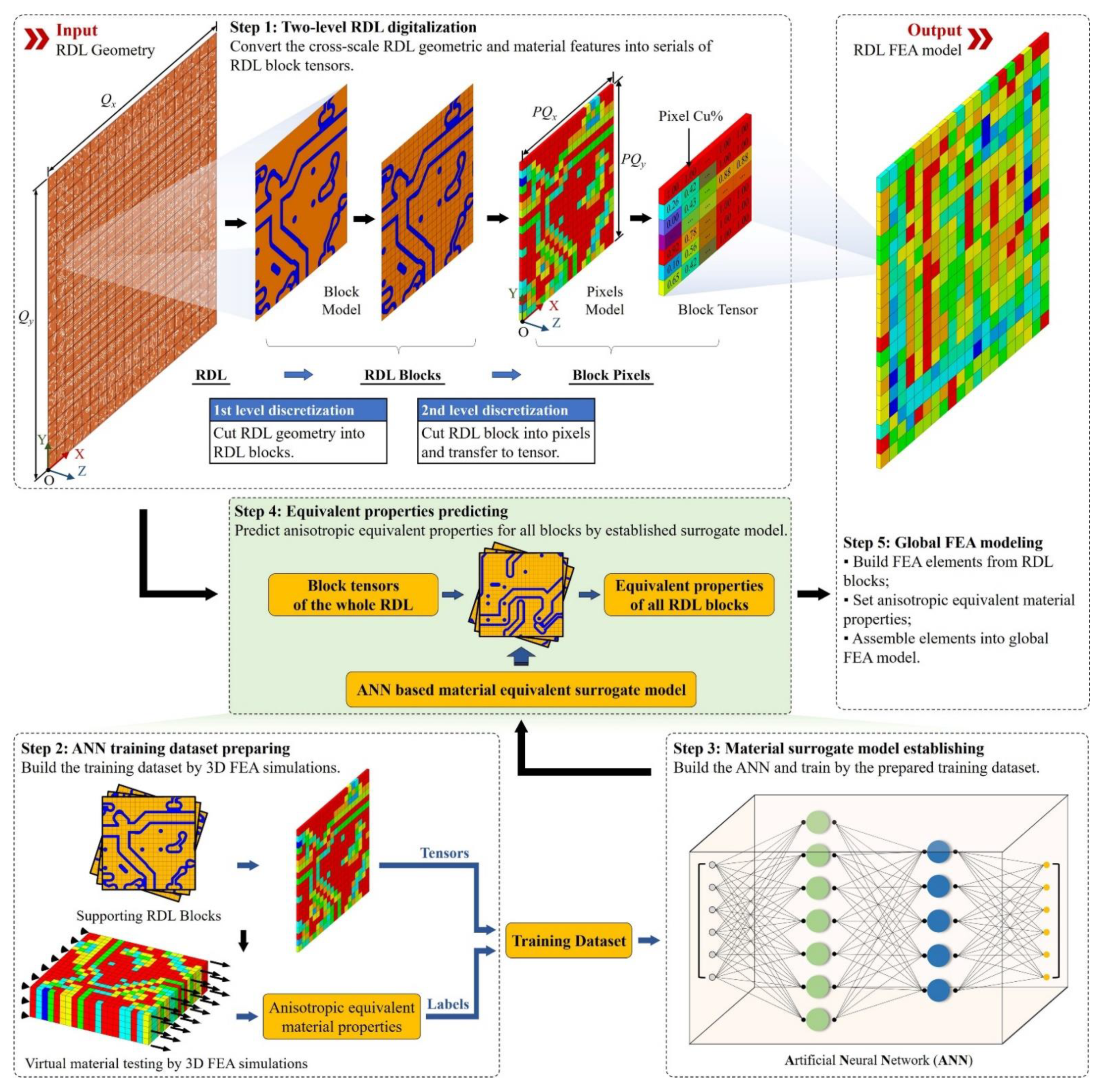
Figure 2.
Full-connected neural network (FCNN) architecture of the proposed method.
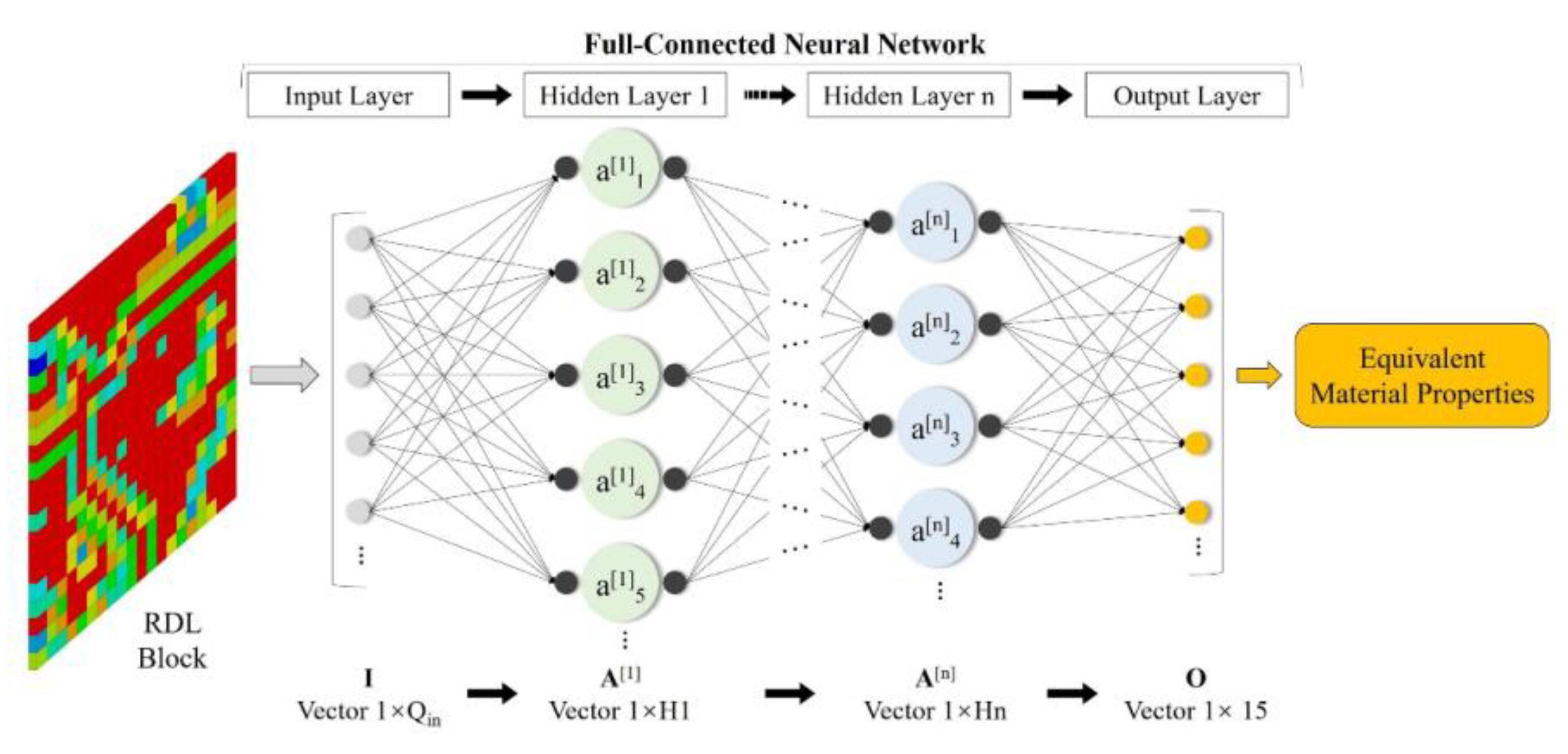
Figure 3.
Convolution neural network (CNN) architecture of the proposed method.
Figure 4.
RDL block augmentation. (a) Initial block, (b) Rotating of 90°, (c) Rotating of 180°, (d) Rotating of 270°, (e) Initial block and flipped in Y, (f) Rotating of 90° and flipping in Y, (g) Rotating of 180° and flipping in Y, (h) Rotating of 270° and flipping in Y.
Figure 4.
RDL block augmentation. (a) Initial block, (b) Rotating of 90°, (c) Rotating of 180°, (d) Rotating of 270°, (e) Initial block and flipped in Y, (f) Rotating of 90° and flipping in Y, (g) Rotating of 180° and flipping in Y, (h) Rotating of 270° and flipping in Y.
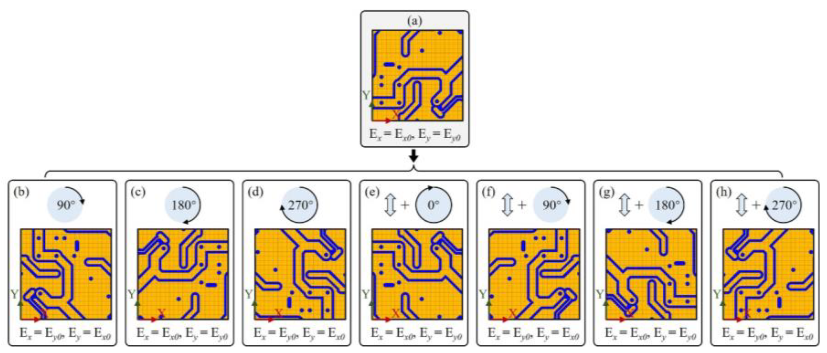
Figure 5.
Model and load cases of the two-layered model bending simulations. (a) Parallel trace bending load case (Case P), (b) Vertical trace bending load case (Case V).
Figure 5.
Model and load cases of the two-layered model bending simulations. (a) Parallel trace bending load case (Case P), (b) Vertical trace bending load case (Case V).
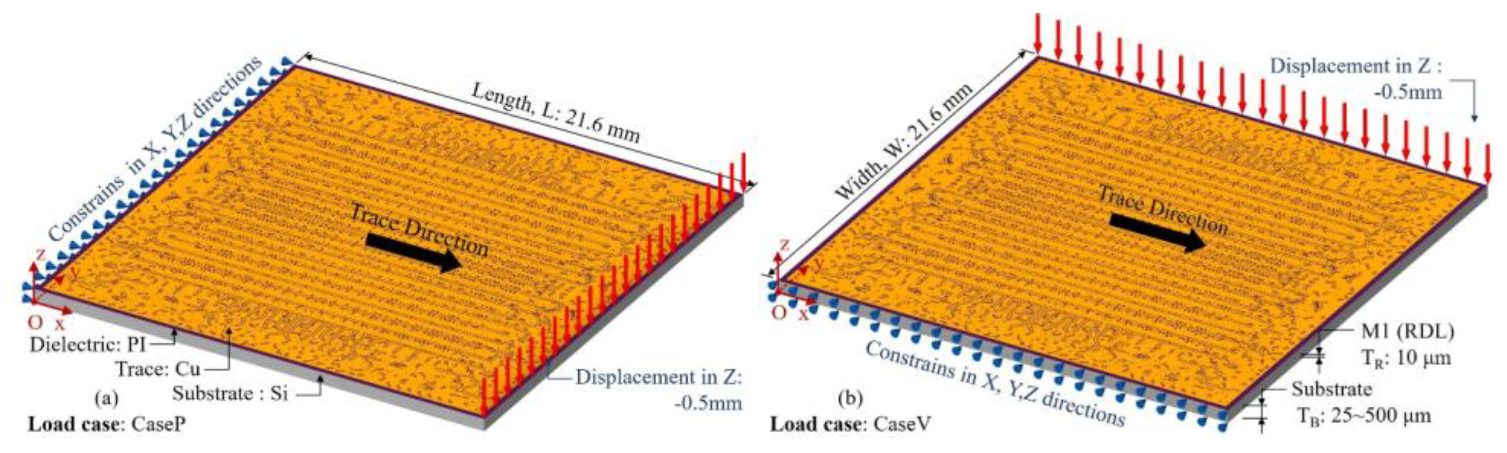
Figure 6.
Layout pattern of M1.
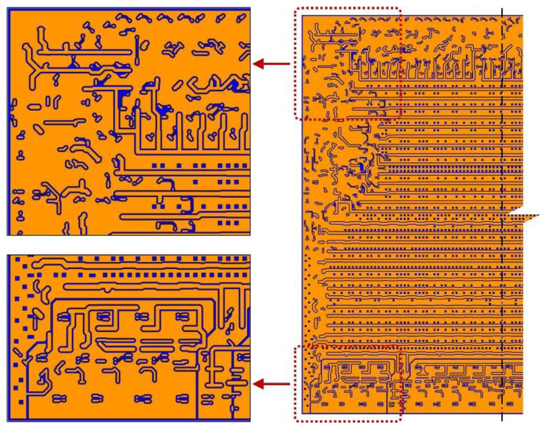
Figure 7.
Von Mises stress distribution of the detailed fine mesh model (The substrate thickness, TB = 50μm). (a) CaseP, (b) CaseV.
Figure 7.
Von Mises stress distribution of the detailed fine mesh model (The substrate thickness, TB = 50μm). (a) CaseP, (b) CaseV.
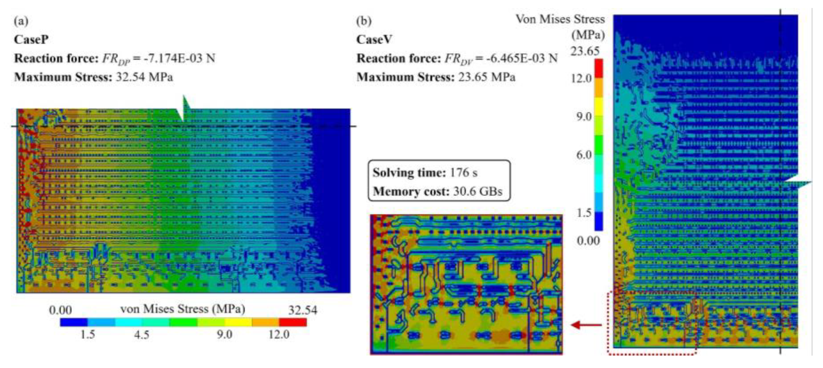
Figure 8.
The loss variation during ANN training and testing procedure.
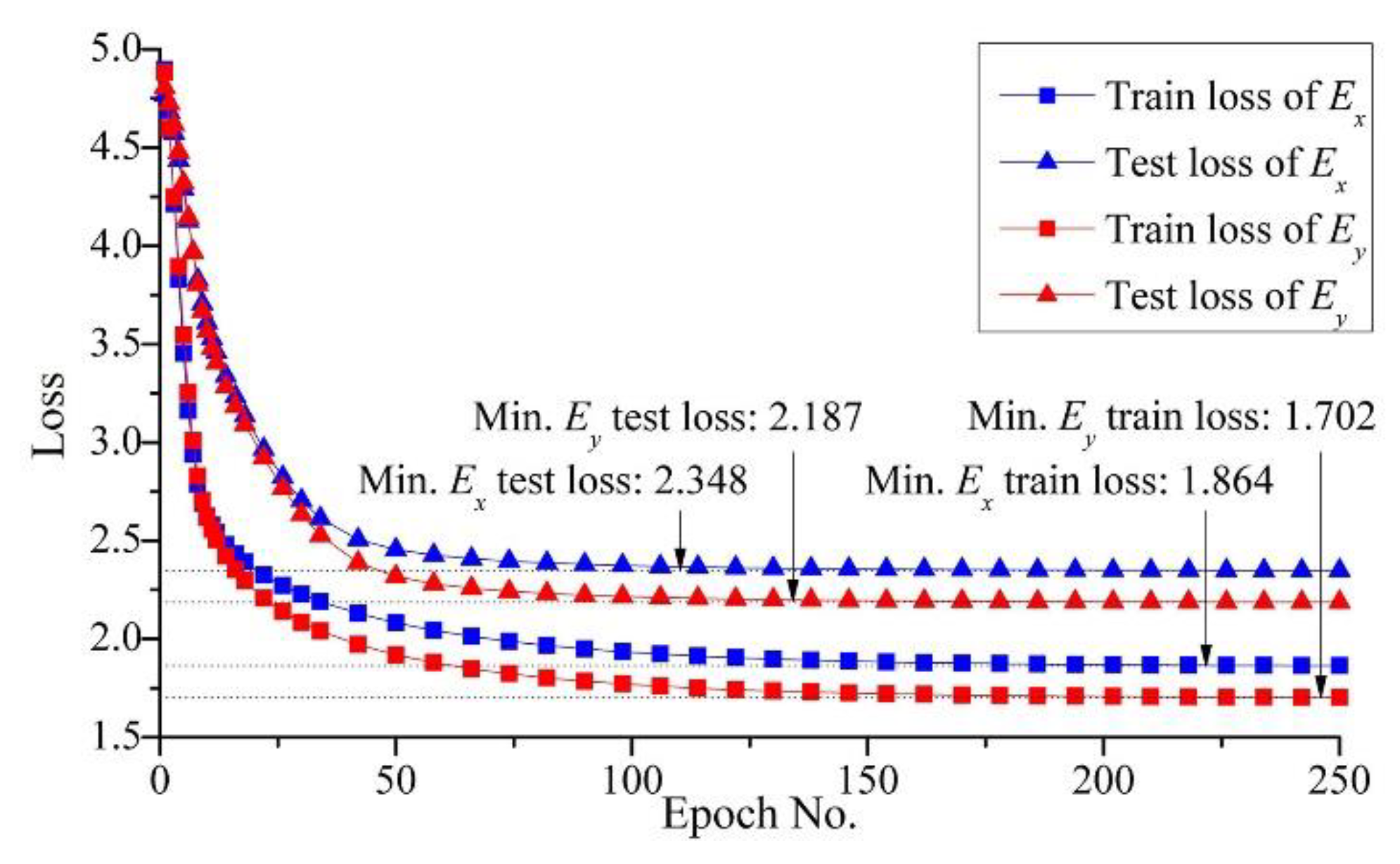
Figure 9.
The anisotropic material of the RDL calculated by simulation-based and ML-based methods.
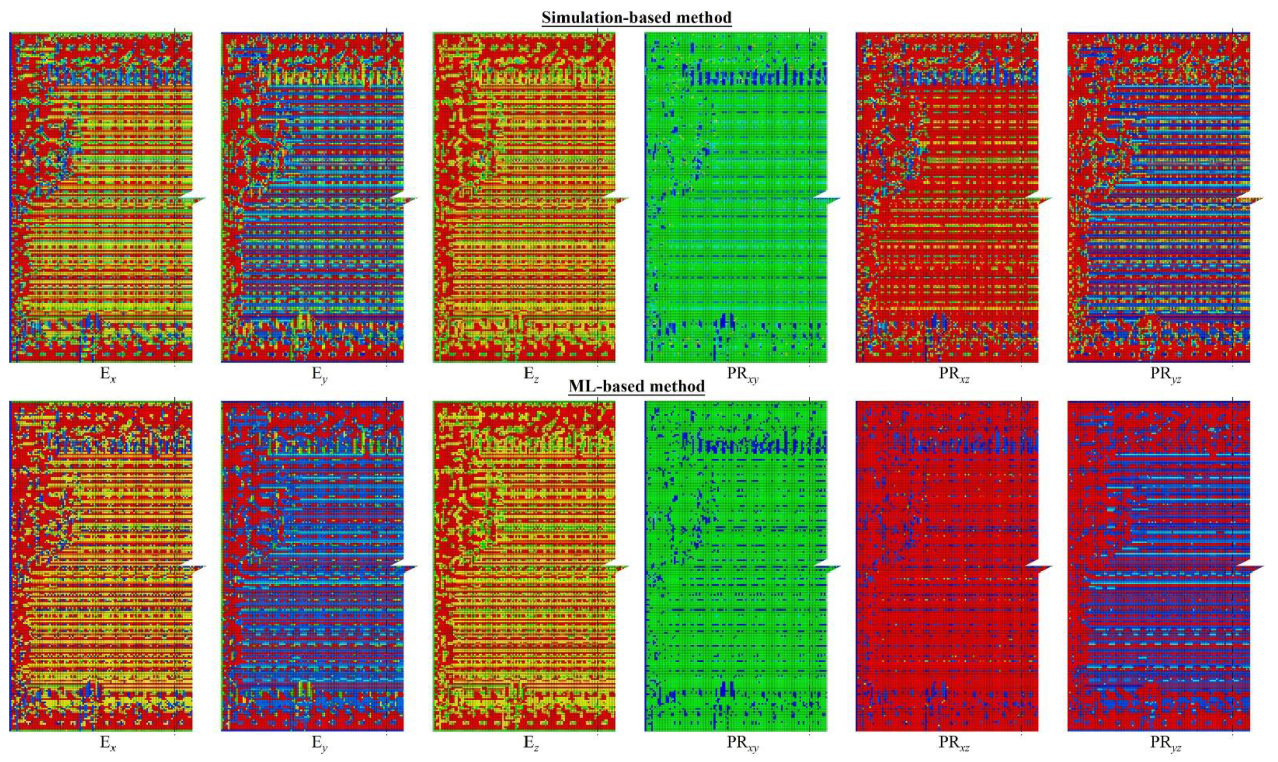
Figure 10.
Von Mises stress distribution of the proposed ML-based modeling method (The substrate thickness, TB = 50μm). (a) CaseP, (b) CaseV.
Figure 10.
Von Mises stress distribution of the proposed ML-based modeling method (The substrate thickness, TB = 50μm). (a) CaseP, (b) CaseV.
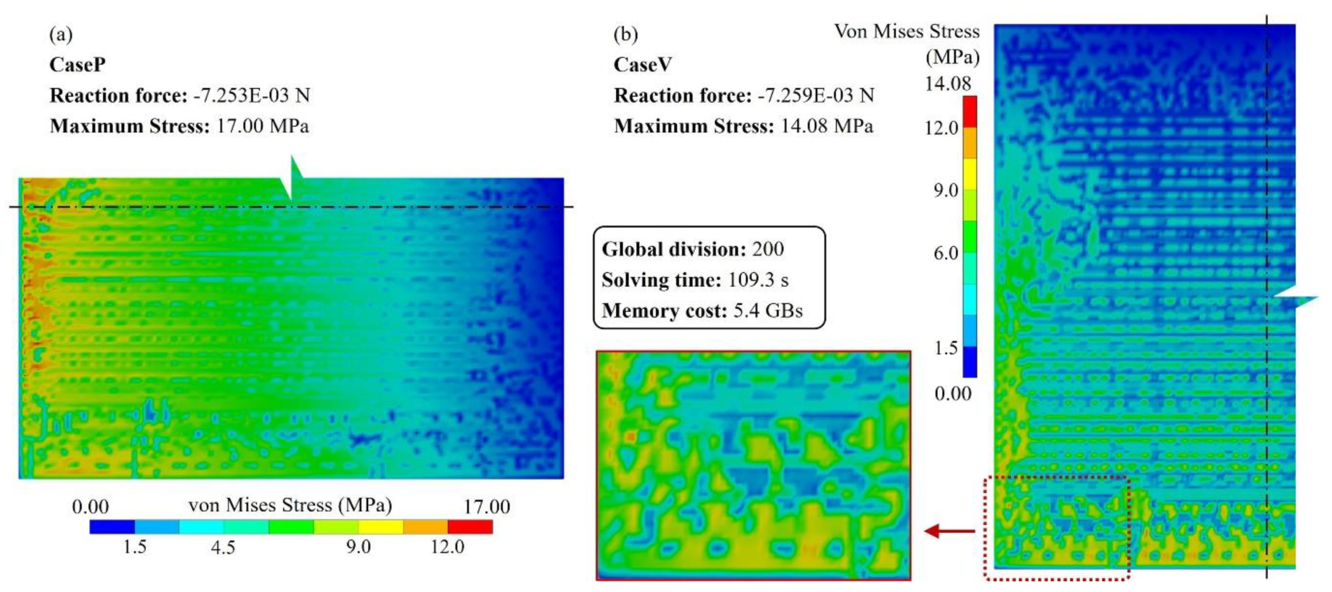
Figure 11.
Boundary conditions and loads for two-layered model warpage simulations.
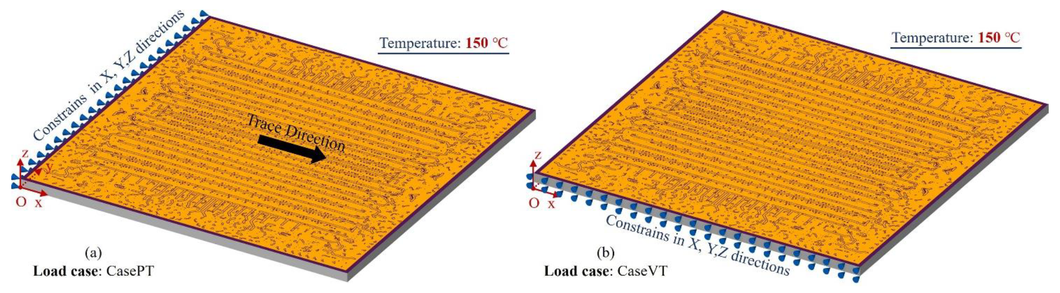
Figure 12.
Result of the parallel trace warpage case (CasePT). (a) Z-direction displacement distribution of the proposed ML-based method, (b) Z-direction displacement distribution of the detailed fine mesh model, (c) von Mises stress distribution of the proposed ML-based method, (d) von Mises stress distribution of the detailed fine mesh model.
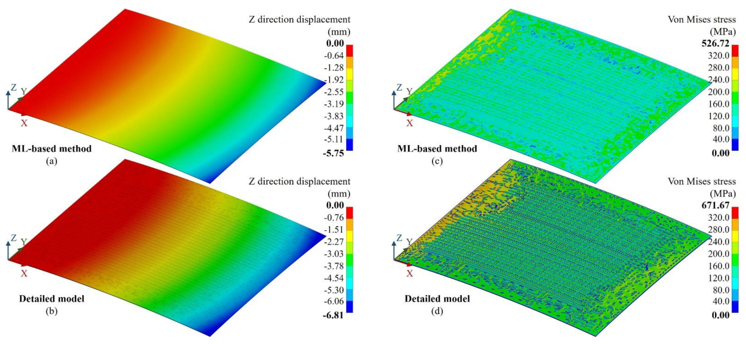
Figure 13.
Result of the vertical trace warpage case (CaseVT). (a) Z-direction displacement distribution of the proposed ML-based method, (b) Z-direction displacement distribution of the detailed fine mesh model, (c) von Mises stress distribution of the proposed ML-based method, (d) von Mises stress distribution of the detailed fine mesh model.
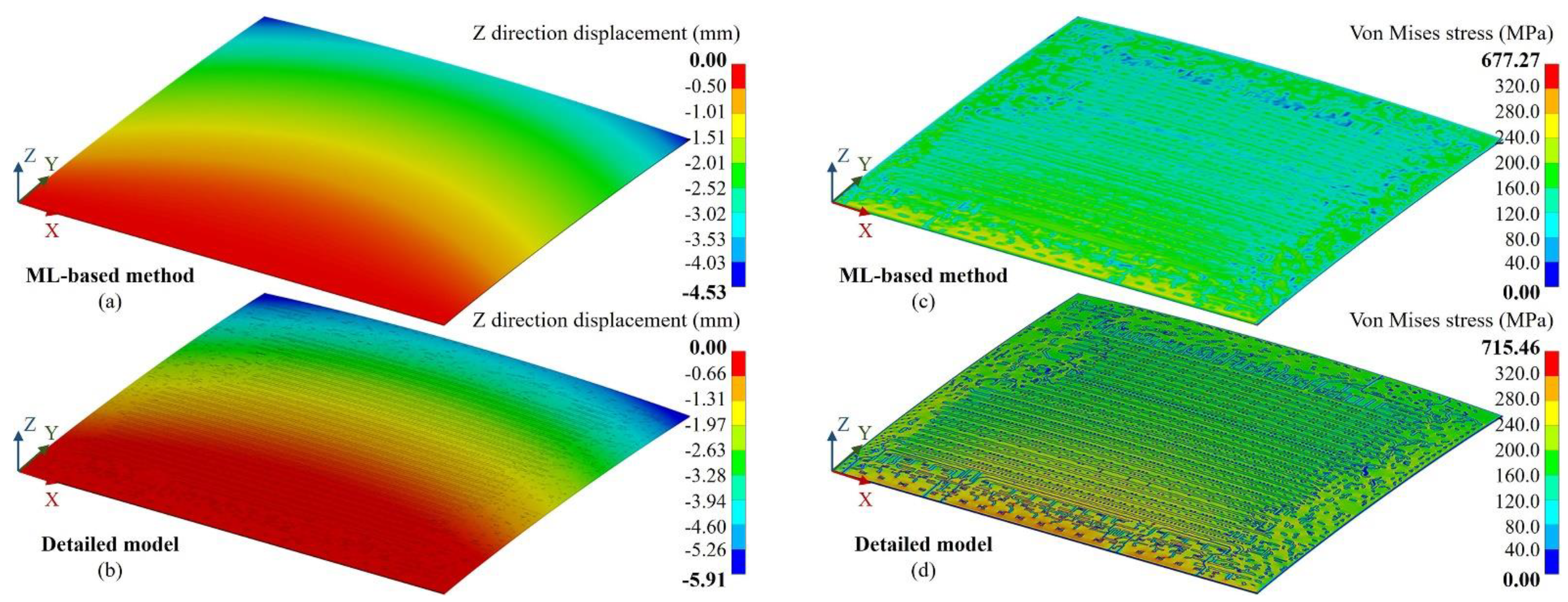
Figure 14.
Reaction force errors of CaseP and CaseV variation by substrate thickness for different modeling methods when global mesh division Q = 200.
Figure 14.
Reaction force errors of CaseP and CaseV variation by substrate thickness for different modeling methods when global mesh division Q = 200.
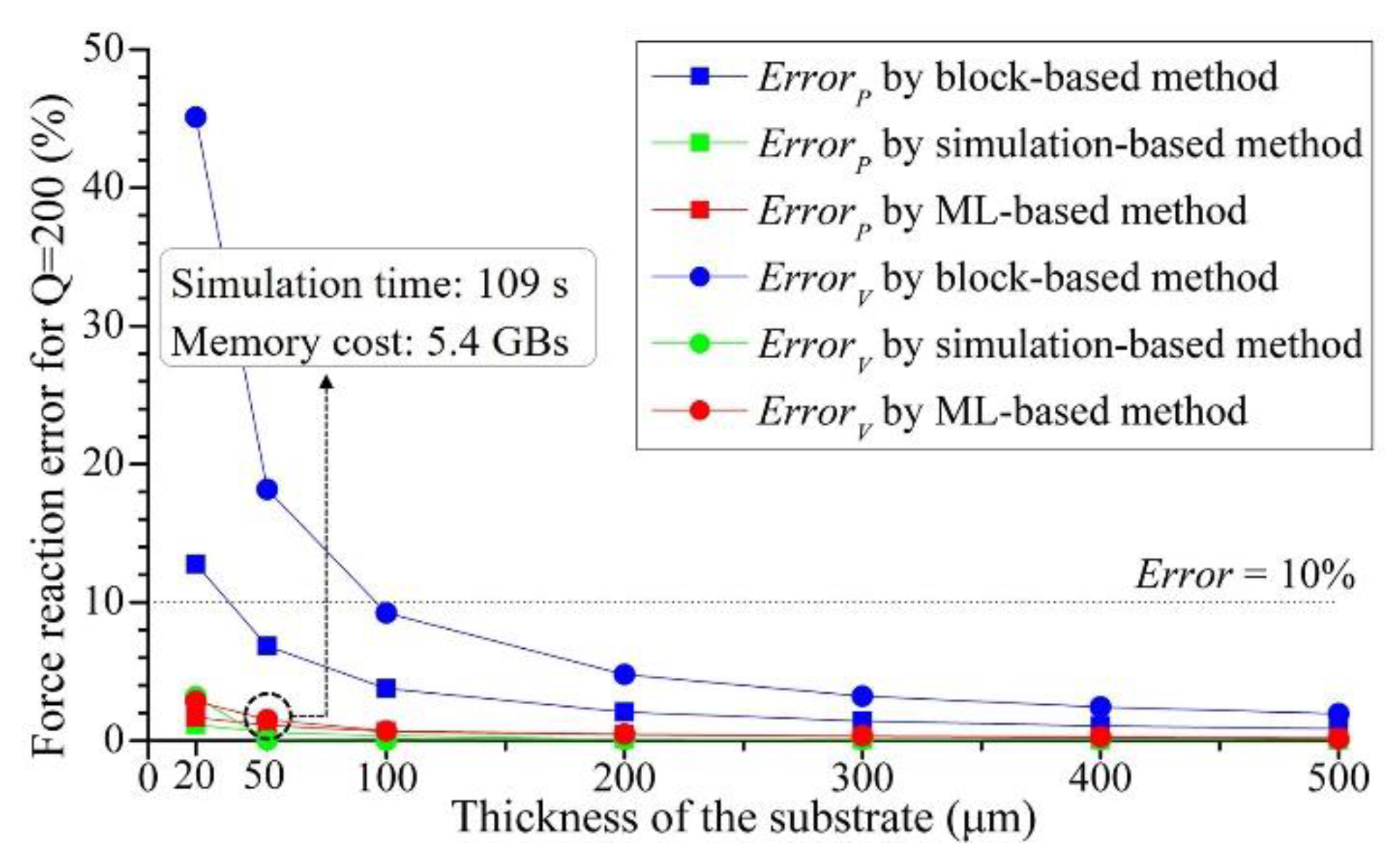
Figure 15.
Reaction force errors of CaseP and CaseV variation by substrate thickness for different global division values. (a) Q = 100, (b) Q = 300.
Figure 15.
Reaction force errors of CaseP and CaseV variation by substrate thickness for different global division values. (a) Q = 100, (b) Q = 300.
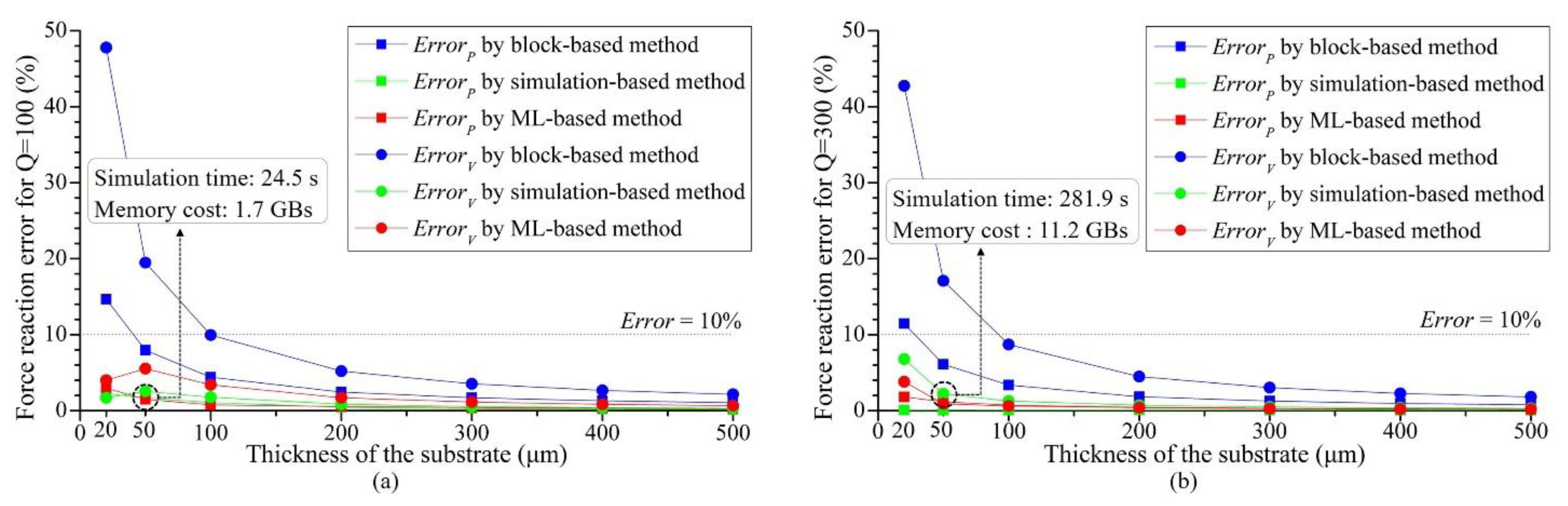
Figure 16.
Von Mises stress distribution of different global mesh division values (The substrate thickness, TB = 50μm). (a) Q = 100, (b) Q = 300.
Figure 16.
Von Mises stress distribution of different global mesh division values (The substrate thickness, TB = 50μm). (a) Q = 100, (b) Q = 300.
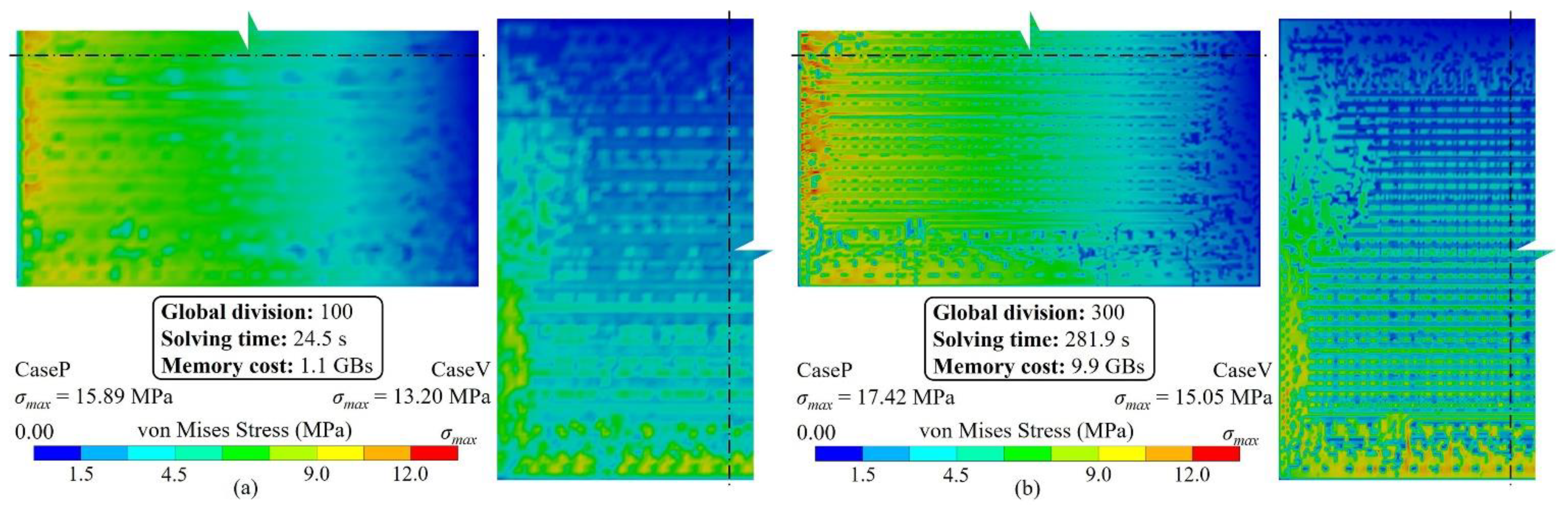
Figure 17.
Reaction force errors and simulation cost of different global mesh division values for the traditional layout neglecting block-based method when the thickness of the substrate equals 50μm.
Figure 17.
Reaction force errors and simulation cost of different global mesh division values for the traditional layout neglecting block-based method when the thickness of the substrate equals 50μm.
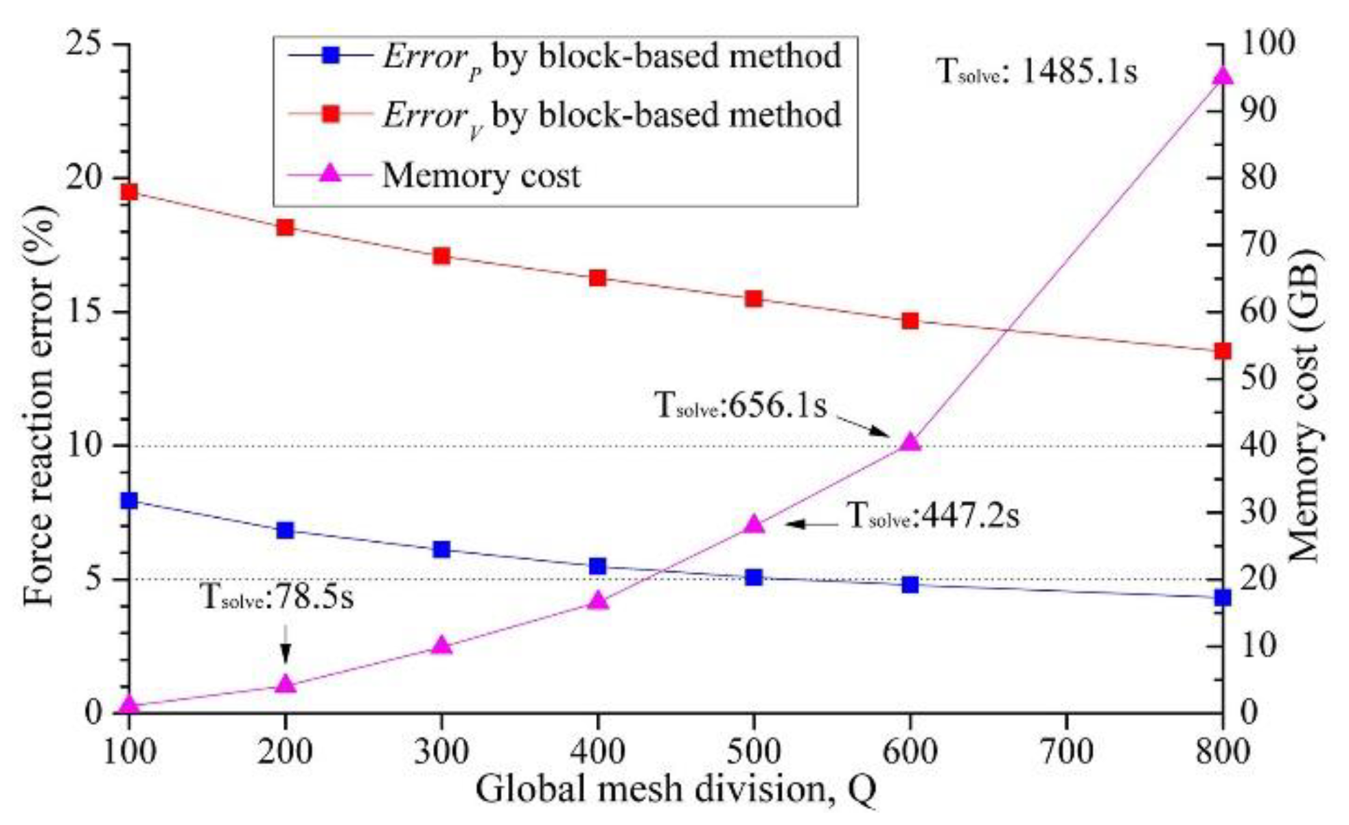
Figure 18.
Von Mises stress distribution of the traditional layout neglecting block-based modeling method of different global mesh division values (TB = 50μm). (a) Q = 200, (b) Q = 600.
Figure 18.
Von Mises stress distribution of the traditional layout neglecting block-based modeling method of different global mesh division values (TB = 50μm). (a) Q = 200, (b) Q = 600.
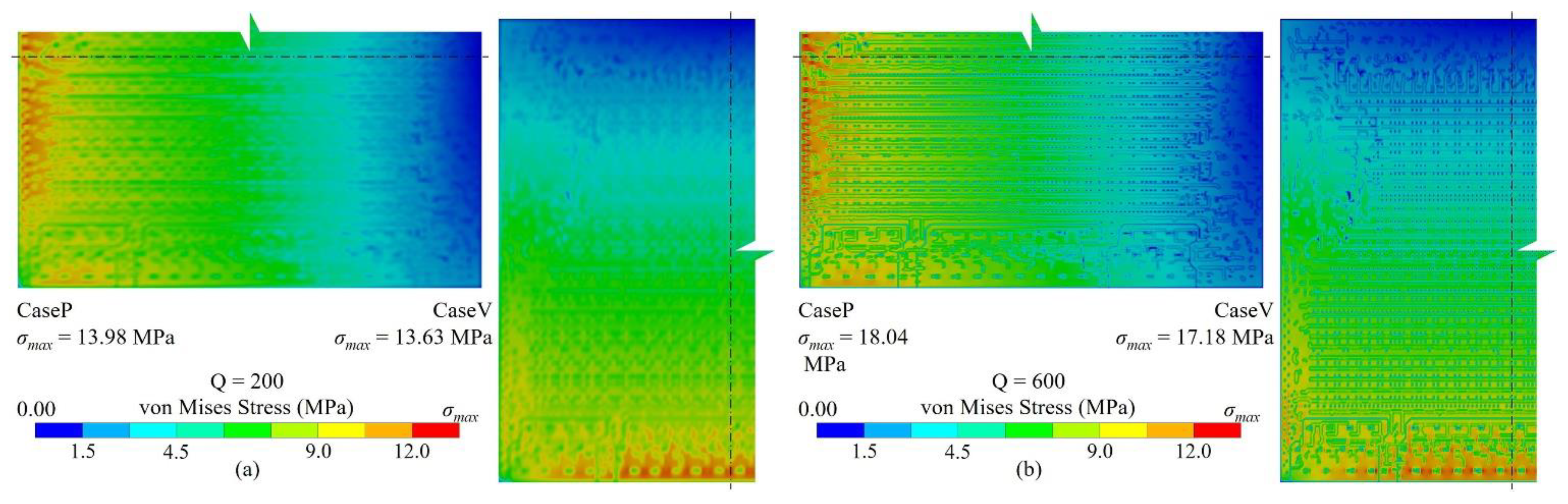
Figure 19.
Loss and training time for different training dataset sizes.
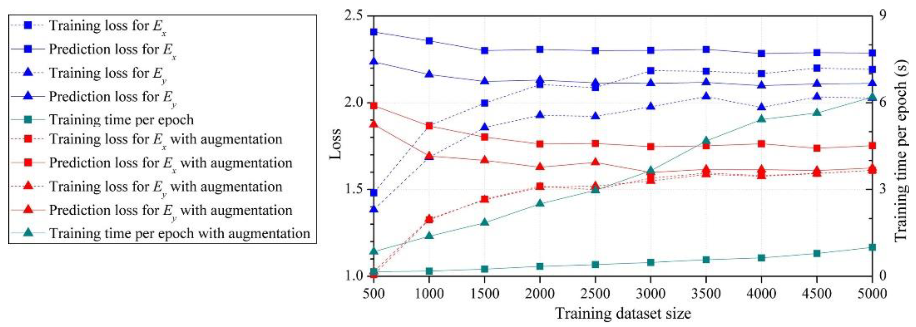
Figure 20.
The anisotropic material of the RDL predicted by the ML-based method with training dataset augmentation.
Figure 20.
The anisotropic material of the RDL predicted by the ML-based method with training dataset augmentation.
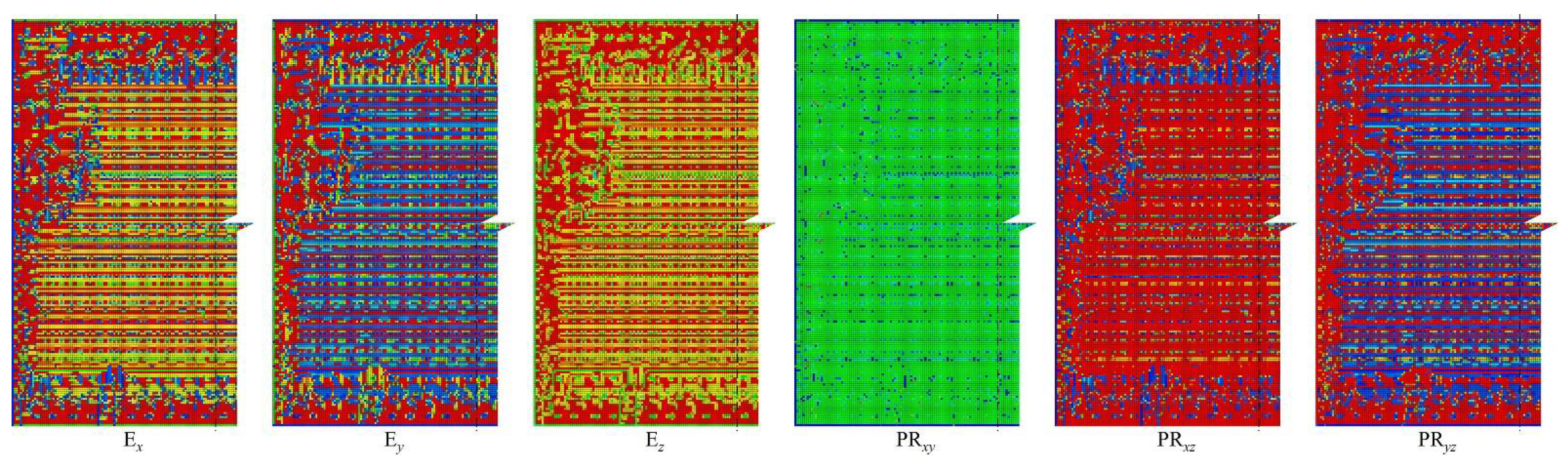
Figure 21.
Training and prediction results of FCNNs. (a) 2 hidden layers FCNNs, (b) 3 hidden layers FCNNs.
Figure 21.
Training and prediction results of FCNNs. (a) 2 hidden layers FCNNs, (b) 3 hidden layers FCNNs.
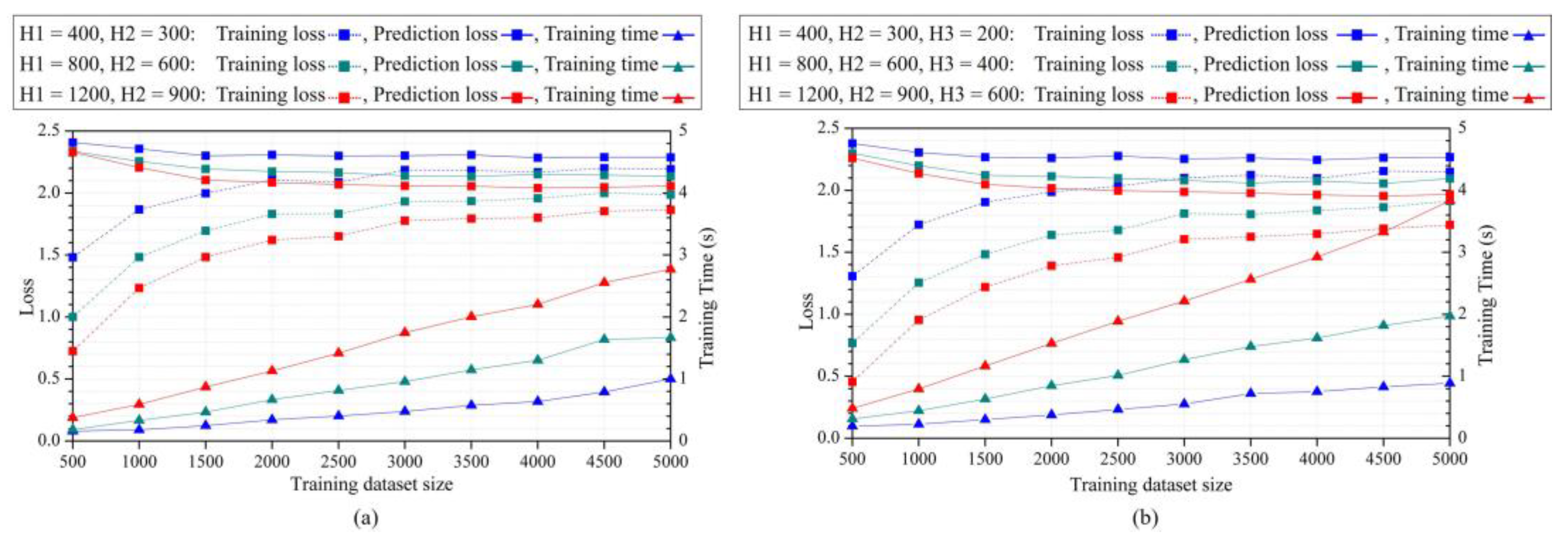
Figure 22.
Prediction and training results of different CNNs.
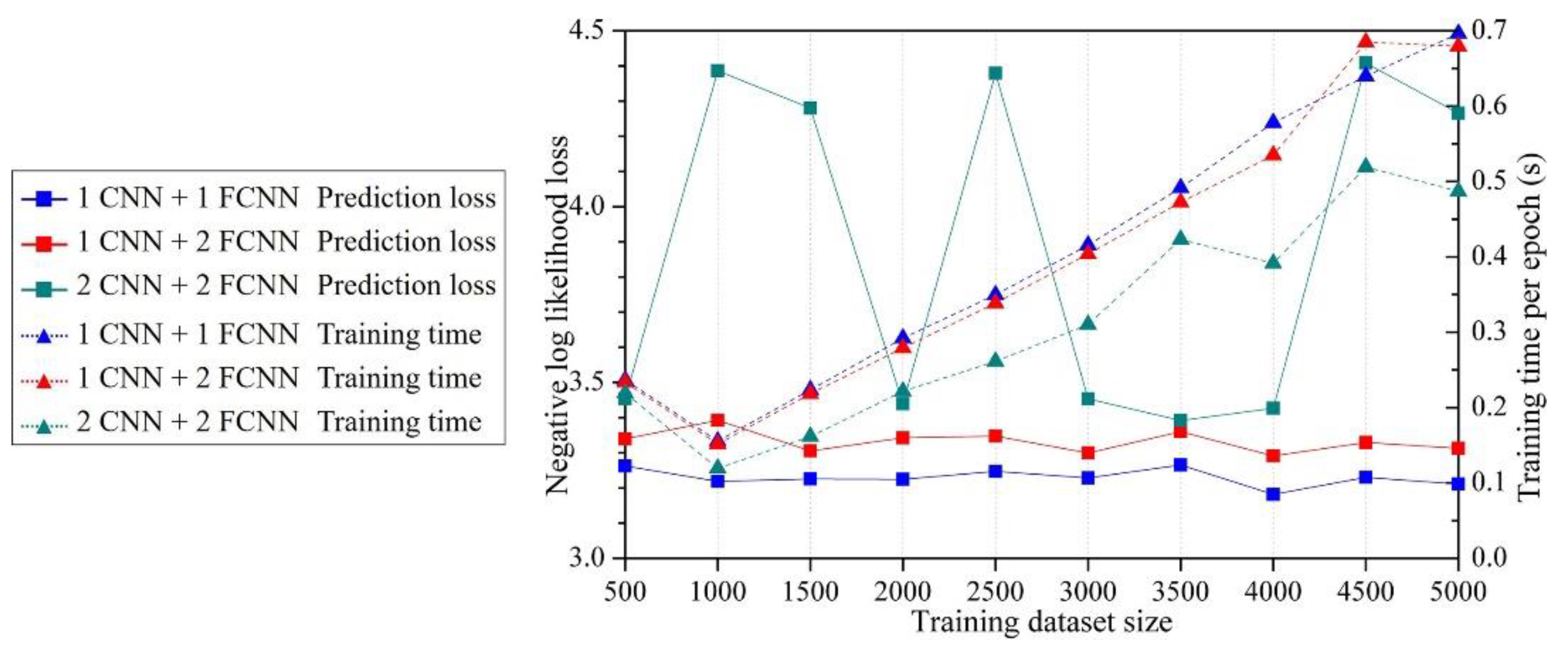
Figure 23.
Geometry model of the 2.5D integrated CPU chip as an application.
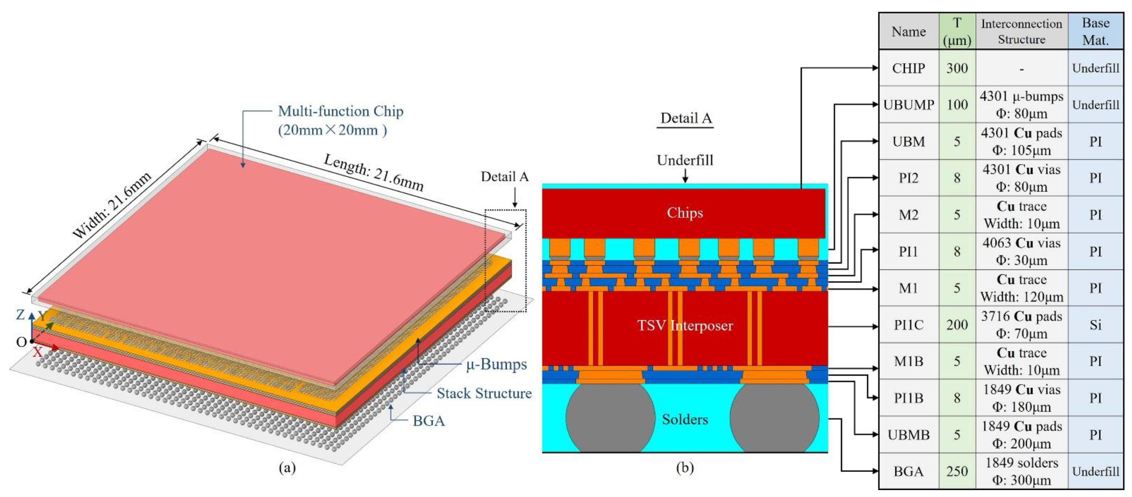
Figure 24.
The maximum temperature state in TCT for the 2.5D integrated CPU chip.
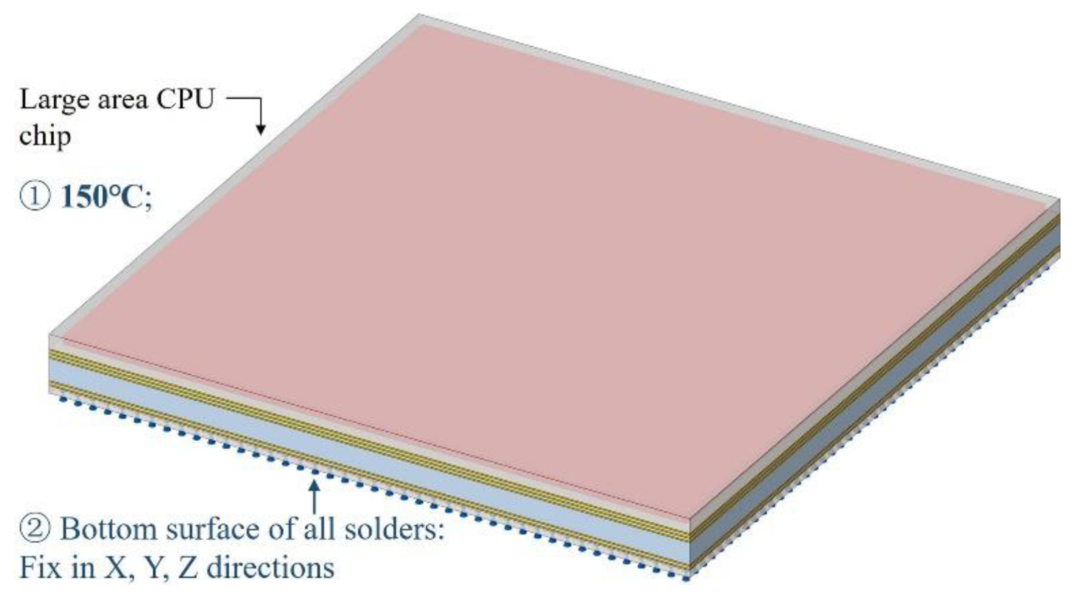
Figure 25.
Von Mises stress distribution of the maximum temperature state of the TCT of the 2.5D integrated CPU chip. (a) Key layers’ stress distributions, (b) M1 stress distribution backgrounded by the layout pattern, (c) Part of the M1 stress distribution, (d) Detail of the maximum stress region backgrounded by the M1 layout pattern and the vias and bumps in adjacent layers.

Disclaimer/Publisher’s Note: The statements, opinions and data contained in all publications are solely those of the individual author(s) and contributor(s) and not of MDPI and/or the editor(s). MDPI and/or the editor(s) disclaim responsibility for any injury to people or property resulting from any ideas, methods, instructions or products referred to in the content. |
© 2023 by the authors. Licensee MDPI, Basel, Switzerland. This article is an open access article distributed under the terms and conditions of the Creative Commons Attribution (CC BY) license (http://creativecommons.org/licenses/by/4.0/).
Copyright: This open access article is published under a Creative Commons CC BY 4.0 license, which permit the free download, distribution, and reuse, provided that the author and preprint are cited in any reuse.


