

Submitted:
30 September 2026
Posted:
01 October 2026
You are already at the latest version
Abstract
Ti₃C₂Tₓ MXene was synthesised via an optimised low-temperature molten salt method using ammonium bifluoride. Complete MAX (Ti3AlC2) phase etching was achieved within 5 minutes at a temperature of 150 °C. Structural and compositional characterisation of Ti₃C₂Tₓ MXene confirmed well-exfoliated Ti3C2Tx sheets with com-plete Al removal. The synthesised Ti₃C₂Tₓ MXene was integrated as the active switch-ing layer in lateral and vertical memristor geometries. Both geometries exhibited non-linear bipolar resistive switching. The vertical device exhibited an on-state current of ~10 mA and stable resistance retention of over 120 minutes. UV-Ozone treatment of lateral devices resulted in the I-V characteristics changing from bipolar to asymmetric with rectifying characteristics. These results establish a broadly accessible, low-cost prototyping framework for Ti₃C₂Tₓ MXene -based memristor devices.
Keywords:
neuromorphic computing
; memristor
; MXene
; 2D nanomaterials
; low-cost memristor fabrication
1. Introduction
Conventional von Neumann computing architectures face increasing challenges to meet the demands of modern artificial intelligence (AI) workloads. In these systems, the physical separation of memory and processing units creates a fundamental bottleneck, limiting both computational throughput and energy efficiency. Neuromorphic computing offers a promising alternative by emulating the parallel, event-driven processing of biological neural network. Within Neuromorphic computers, memristors are widely explored as candidate synaptic elements, owing to their programmable resistance states for encoding neural weights [1].
The building block of a memristor is an active switching layer, for which two-dimensional (2D) materials have emerged as a strong candidate. Among 2D emerging materials for neuromorphic hardware, 2D transition metal carbides and nitrides, collectively known as MXenes, have garnered significant attention. Their exceptional metallic conductivity, tunable surface chemistry, and compatibility with thin-film device architecture make them strong candidates for active device layers. MXenes are derived from ceramic MAX phase precursors. The MAX phases follow the general formula Mn+1AXn, with M being an early transition metal, A is an A-group element (typically Al or Si), and X is either carbon or nitrogen. MXenes are synthesised through the selective etching of the A layer from MAX phase. The resulting MXene follows the formula Mn+1XnTx, where Tx denotes surface terminations such as -OH, -O, and -F which are introduced during the etching process. This diverse elemental composition may allow the tunability of electrical and interfacial properties. The most extensively studied MXene is Ti₃C₂Tₓ which is derived from the Ti₃AlC₂ MAX phase by removal of the Al layer[2,3,4,5,6,7,8,9]. MXene high metallic conductivity and redox-active surface terminations facilitate ion migration and localised conductive filament formation under applied electric fields. These properties make Ti₃C₂Tₓ a promising active layer material for memristive devices.
MXene based memristors devices usually comprise two conductive electrodes sandwiching MXene in the vertical configuration or on the opposite ends of a MXene film for planar devices. The resistive switching in Ti3C2Tx-based memristor devices, for both configurations, have been attributed to the formation and rupture of conductive filaments through the MXene film. The filaments are either due to ion migration or localised redox processes at the electrode-MXene interface[10]. The surface termination chemistry of MXene plays a critical role in modulating the memristive operation. The termination groups (-O, -OH and -F) can act as defect and trap sites turning pristine Ti₃C₂Tₓ into a viable active switching layer without the need for hybridisation with secondary materials [11,12,13]. Hybridisation approaches adds fabrication complexity, introducing interfacial variability, and complicating device scalability. However, pristine Ti₃C₂Tₓ circumvents these limitations, offering a single-material active switching layer without the need for secondary phases. The surface terminations of pristine Ti₃C₂Tₓ can be altered using post-synthesis treatment, directly tuning its electrical properties and memristive performance [7,14].
Widespread adoption of MXenes for applications in devices is constrained by the challenges in their synthesis. Most established etching routes employ concentrated hydrofluoric acid (HF) [15]. This approach introduces severe handling hazards, stringent infrastructure requirements, significant environmental disposal concerns, batch to batch variability, and low yields. Alternative methods, such as hydrothermal etching using lithium fluoride and hydrochloric acid (LiF/HCl), reduce direct HF exposure by generating HF in situ. However, they typically require extended reaction times ~45 hours and elevated pressures, which limited scalability[16]. Lewis acid molten salt (LAMS) etching has emerged as a fluorine-free alternative for MXene synthesis, however, LAMS typically requires temperatures exceeding 550 °C and reaction durations of 24 hours or more[17]. In contrast, low-temperature molten salt (LTMS) synthesis using ammonium bifluoride (NH₄HF₂) reduces the need for direct handling of concentrated HF while enabling faster etching under lower-temperature conditions as reported by Wang et al.[18] They demonstrated that efficient MAX phase etching was achievable within minutes at lower temperatures, 130 °C, thus, significantly reducing both reaction time and hazards relative to previous methods [18].
Equally important to synthesis is the simplicity of memristor device fabrication. MXene thin film deposition for memristor applications has predominantly relied on spin coating, which provides controlled film thickness and high flake alignment. However, it requires precise parameter optimisation and yields films sensitive to substrate hydrophilicity. Electrode patterning has typically relied on shadow masking, which is equipment-minimal but limited in resolution, or conventional photolithography, which offers higher precision but requires cleanroom infrastructure and multi-step chemical processing[6,19]. Dry film photoresist (DFR) offers a compelling alternative: a solid polymer laminate that is applied by roller lamination without the need for spin coating, no requirement for a cleanroom environment, and is widely used in low-cost printed circuit board (PCB) and microfluidic device fabrication[20]. Despite its use in PCB and microfluidic fabrication, DFR remains underexplored as a low-cost patterning route for MXene-based memristor prototypes.
The choice of device geometry is a further key variable in memristor behaviour. In a lateral configuration, co-planar electrodes impose a horizontal current path along the MXene film, promoting lateral filament growth and offering simple, shadow-mask-compatible test architecture[21]. While in a vertical configuration, current is directed perpendicular to the film through a sandwiched electrode stack, confining filament formation to the film thickness. Comparing both geometries from a single material system under identical synthesis conditions enables direct assessment of how memristor architecture governs switching behaviour independently of material variability[22,23].
In this work, Ti₃C₂Tₓ MXene was synthesised via an adapted and optimised low-temperature molten salt method. The as-synthesised Ti₃C₂Tₓ MXene was then integrated as the active switching layer in two device geometries: lateral memristor and vertical memristor. The effect of surface termination engineering on the lateral memristor behaviour is investigated.
2. Materials and Methods
2.1. MXene Synthesis
The Ti₃C₂Tₓ MXene synthesis process as shown in Figure 1 comprises five main steps: ball milling, vacuum drying, molten salt etching, washing, and vacuum drying. Ti₃AlC₂ MAX phase powder (1.0 g; Nanochemazone, Canada) and anhydrous NH₄HF₂ flakes (6.0 g; Fisher Scientific, UK) were combined in a 1:6 mass ratio and loaded into a Teflon milling jar. The mixture was then milled using a Retsch CryoMill at room temperature at 20 Hz for 10 minutes. The homogeneous mixture enhances the interfacial contact between the MAX phase and NH4HF2. Due to the to the hygroscopic nature of NH4HF2, the milled mixture was dried under vacuum ~20 mbar for 12 hours, ensuring removal of any possible residual moisture The resulting Ti₃AlC₂/NH₄HF₂ mixture was transferred to a two-neck PTFE round bottom flask and purged with Ar for ~ 2 hours to establish inert conditions and mitigates against in-situ oxidation of the desired Ti₃C₂Tₓ MXene product.
The reaction setup as illustrated in Figure 1 comprises a PTFE flask and a PTFE reflux condenser as they are chemically inert to active fluoride species [23]. An oil bath is preheated to 150 °C prior to initiating the reaction, with continuous magnetic stirring prior to initiating the reaction.
The etching reaction proceeds as expressed in equation 1:
Ti3AlC2 + 3NH4HF2 → Ti3C2Tx + (NH4)3AlF6 + 1.5 H2
(1)
From equation (1), the reaction yields Ti₃C₂Tₓ MXene as the primary product, alongside (NH₄)₃AlF₆ as a soluble by-product salt and hydrogen (H₂) as a gaseous by-product which is removed by the inert carrier gas. The PTFE flask, with the reactants, is subsequently submerged in the hot oil bath. The reaction mixture with the flask rapidly transforms into a foam-like mixture with vigorous hydrogen evolution for 5 minutes. The release of gas evolution indicated the completed etching of the MAX phase. The flask was then removed from the oil bath to allow the reaction mixture to cool to room temperature. The resultant product was then washed repeatedly with DI water to remove the by-product salts, where each wash cycle consisted of dispersing the etched crude Ti₃C₂Tₓ. in DI water, centrifuging at 3500 rpm for 5 minutes, and decanting the supernatant. DI water washing continued until the pH of the supernatant reached approximately 7. Then further washing was performed with ethanol 5 times, using the same steps as with DI water, to displace any residual water to assist the drying process and remove any potential oxidative degradation of the Ti₃C₂Tₓ MXene sheets. The Ti₃C₂Tₓ MXene was then dried under vacuum at room temperature for ~12 hours.
2.3. Memristor Fabrication
Two memristor geometries were fabricated using the as-synthesised Ti₃C₂Tₓ MXene: a vertical stack and a lateral configuration. For MXene film deposition, the as-synthesised Ti₃C₂Tₓ MXene powder was redispersed in DI water at a concentration of 10 mg mL⁻¹. The dispersion was bath-sonicated for 60 minutes to promote homogeneity and delamination into individual or few-layer flakes, yielding a stable colloidal suspension. The resulting dispersion was used for both memristor geometries without further modification. MXene dispersion was drop-casted on to the substrate and spin-coated at 100 rpm for 300 seconds resulting in a continuous thin film.
For the lateral memristor, the Ti₃C₂Tₓ MXene dispersion was deposited directly onto a bare Si substrate, forming an active film area of approximately 6 mm². No attempt was made to remove SiO2 native layer. The MXene coated substrate was subsequently dried under ambient conditions to evaporate DI water. Pt and Ag electrodes were then deposited on either side of the Ti₃C₂Tₓ MXene film by magnetron sputtering, with an inter-electrode gap of approximately 1 mm. For the vertical memristor, the Si substrate was first coated with a 2 nm Ti adhesion layer followed by an 80 nm Pt bottom electrode via magnetron sputtering. Active memristor areas were then defined using a negative-tone dry film photoresist (DFR) patterning process. The DFR layer was laminated onto the Si/Ti/Pt substrate using an office roller laminator, applying uniform heat and pressure to achieve conformal adhesion across the substrate surface. The laminated substrate was subsequently placed beneath a photomask defining the desired memristor window geometry and exposed to UV light at 380 nm. Development was carried out by immersion in a 1% w/v potassium carbonate solution, which selectively dissolves the unexposed resist and reveals the underlying Pt surface within the patterned windows. The substrate was rinsed with DI water and dried prior to Ti₃C₂Tₓ MXene deposition.
The Ti₃C₂Tₓ MXene dispersion was then drop-cast into the patterned windows and dried under ambient conditions to form the active switching layer. An 80 nm Ag top contact was subsequently deposited by magnetron sputtering. The complete stacked structure bottom to top has the following configuration; Si/Ti/Pt/Ti3C2Tx/Ag. characterisation for both memristor geometries was performed using a Keithley 2400 source-measure unit (SMU) in a two-probe configuration.
3. Results and Discussion
3.1. Material Characterisation
The structural and compositional properties of the as-synthesised Ti₃C₂Tₓ MXene were characterised using a combination of scanning electron microscopy (SEM), X-ray diffraction (XRD), energy-dispersive X-ray spectroscopy (EDX), and Raman spectroscopy.
The XRD of the as-synthesised Ti₃C₂Tₓ MXene, and the corresponding MAX phase were collected over a 2θ range of 5° to 90° to examine the structural transformation following synthesis as shown in Figure 2(a). The Ti₃AlC₂ MAX phase, the black line in Figure 2(a), displays characteristic diffraction peaks at 9.54° and 39.06°, corresponding to the (002) and (104) reflections, respectively[15]. This confirms the MAX phase well-ordered layered structure. For Ti₃C₂Tₓ MXene XRD (red line), this reflection at (104) is absent, confirming the selective and complete etching of the Al layer hence loss of the MAX phase periodicity. The XRD pattern of Ti₃C₂Tₓ MXene is dominated by the (002) reflection. This peak shifts to a lower angle, from 9.54° 2θ for the MAX phase to 6.52° 2θ for the MXene. Interestingly, this (002) of MXene is also lower than the value of 6.94 reported for the standard LTMS method[18]. This may be attributed to greater interlayer expansion during the Al removal process due to the enhanced interfacial contact between the NH₄HF₂ salt and the MAX phase by ball milling, promoting a more efficient intercalation of reaction species between the MAX phase layers on reaction.
The interlayer spacing between MXene sheets, d-spacing. was calculated from the (002) peak position using Bragg's law. For these samples, the d-spacing was in the range of 13.3 Å.
To identify the bonding character of each material and confirm the structural transformation following synthesis, the Raman spectra of Ti₃AlC₂ MAX phase (black line) and Ti₃C₂Tₓ MXene (red line), as shown in Figure 2(b), were acquired. The MAX phase spectrum exhibits two broad features at wavenumbers of approximately 270 and 560 cm⁻¹, characteristic of Ti-Al-C vibrational modes [24], whilst the Ti₃C₂Tₓ MXene spectrum exhibited four distinct vibrational modes, labelled as ω₁ - ω₄ at 140, 236, 440, and 606 cm⁻¹ respectively.
The ω₁ mode at 140 cm⁻¹ is associated with Ti-C vibrations within the Ti₃C₂Tx layers [25]. The ω₂ mode at 236 cm⁻¹, accompanied by a notably enhanced intensity, is consistent with the influence of fluorine surface terminations introduced during etching [15]. The ω₃ mode at 440 cm⁻¹ is another intense peak in the Ti₃C₂Tₓ MXene spectrum that is absent in the MAX phase, confirms the formation of oxygen-containing surface terminations [26]. The ω₄ mode at 606 cm⁻¹ can be attributed to carbon layer vibrations, with secondary contributions from Ti-O and Ti-F stretching [27]. These modes are distinctly different to the MAX phase spectrum and confirm the successful transformation of Ti₃AlC₂ to Ti₃C₂Tₓ.
The surface morphology of the as-synthesised Ti₃C₂Tₓ MXene was observed using SEM as seen in Figure 3(a). The SEM image of Ti₃C₂Tₓ MXene on the Si substrate reveals accordion-like layered structure, characteristic of well exfoliated Ti₃C₂Tₓ MXene. MXene dispersed on a TEM grid, revealing thin translucent MXene sheets, with well-defined lateral dimensions and clear sheet-like contrast as shown in Figure 3(b). These features are characteristic of few-layer or single-layer MXene flakes and further confirm successful exfoliation of MXene. Figure 3(c) shows elemental maps of a single Ti₃C₂Tₓ MXene flake. The elemental composition of the Ti₃AlC₂ MAX phase and the synthesised Ti₃C₂Tₓ MXene are summarised in Table 1. The values in Table 1 were obtained by averaging measurements from multiple points on different flakes to improve compositional representativeness. For Ti₃AlC₂, EDX analysis gave Ti, Al, and C contents of 58.07%, 11.37%, and 30.56%, respectively, which is consistent with the expected MAX phase stoichiometry. The Ti₃C₂Tₓ MXene showed Ti, C, O, and F contents of 43.90%, 26.34%, 15.63%, and 14.13%, respectively. The Ti and C signals are consistent with the MXene lattice, while the O and F signals reflect surface terminations introduced during the etching process. The absence of Al confirms effective removal of the A-layer and successful conversion from Ti₃AlC₂ to Ti₃C₂Tₓ. No Al signal was detected in any of the elemental maps, confirming complete removal of the Al layer.
3.2. Electrical Measurements of Memristors
For all electrical measurements, the silver contacts were selected as the positive electrode. The lateral memristor exhibits a strongly non-linear, symmetric bipolar I-V characteristic. Current remains suppressed near zero bias, falling below 10⁻⁵ mA at approximately 100KΩ, and rises sharply and symmetrically in both voltage polarities beyond approximately 1–2 V, reaching ~1 mA at ±6 V. The smooth, continuous nature of the current onset, and the absence of any discrete SET or RESET transitions, is consistent with a field-driven conduction mechanism rather than abrupt filamentary switching [4]. The cycling stability of the device was evaluated by carrying out over 100 consecutive voltage sweeps. The overlaid I-V curves demonstrate excellent cycle-to-cycle uniformity, with the 100-sweep ensemble closely reproducing the first sweep across the full voltage range. This confirms the reproducibility and stability of the lateral memristor under repeated electrical stress.
The vertical Ag/Ti₃C₂Tₓ/Pt/Ti/Si memristor similarly exhibits a nonlinear, symmetric bipolar characteristic. The off-state resistance near zero bias is elevated at approximately 1 MΩ, whilst the on-state current at ±6 V reaches ~10 mA, exceeds that of the lateral memristor by approximately one order of magnitude. This enhanced on-state conductance is attributed to the vertical current path through the Ti₃C₂Tₓ MXene film thicknesses. The grey region in Figure 4(b) shows the 100 consecutive sweeps. The 100-sweep overlay shows moderate variation in the transition region. Resistance retention was monitored over 120 minutes following completion of the 100-sweep I-V. The device showed stable resistance over this period, as seen in the inset of Figure 4(b). The plotted resistance reflects the natural device state retained after repeated voltage sweeping. The device resistance was sampled at a read voltage of 0.1 V and remained stable at approximately 100 kΩ throughout the measurement window, with only minor fluctuations attributable to measurement noise.
3.3. Effect of UV-Ozone Treatment on Ti₃C₂Tₓ MXene Planar Memristors
To investigate the effect of controlled surface modification on memristor behaviour, the Ti₃C₂Tₓ MXene lateral memristor was subjected to UV-ozone (UV-O₃) treatment for 6 hours prior to electrode deposition. UV-ozone treatment generates reactive atomic oxygen species that selectively convert surface terminations, promoting the replacement of -F and -OH groups with -O terminations[7].
The Raman spectra of pristine (black curve) and UV-O₃-treated (red curve) Ti₃C₂Tₓ are shown in Figure 5(a). Following UV-O₃ treatment, a pronounced broadband attenuation of all Raman modes is observed. The ω₃(O/F) peak at ~440 cm⁻¹ and the ω₄(C) peak at ~606 cm⁻¹ are nearly fully suppressed, and the ω₁(Ti) and ω₂(Ti-C) modes are significantly attenuated. This intensity reduction across all modes reflects significant disruption to the near-surface Ti₃C₂Tₓ structure, consistent with extensive modification of the surface termination chemistry. As observed by the Raman spectra, the increased density of -O terminations introduced by UV-O₃ exposure is known to localize electrons at Ti sites, reducing the effective carrier density of the MXene and increasing its sheet resistance relative to the -F and -OH terminated pristine material[26,28]. The UV-O₃-treated spectra shows attenuation and shift of the existing Ti₃C₂Tₓ Raman modes, but no additional peaks attributable to crystalline TiO₂ are observed. This suggests that the treatment modifies the MXene surface and termination chemistry, rather than producing a clearly detectable TiO₂ phase.
The electrical response of the UV-O₃-treated MXene planar memristor (Figure 5(b)) in contrast to the pristine planar memristor, exhibits a strong asymmetric rectifying I-V characteristic over the ±8 V measurement range. The current through the device remains suppressed at approximately 10⁻⁶ mA across the entire negative voltage range. A sharp step increase in the current occurs close to 0 V as the positive voltage is swept. The current reaches a saturation value of ~10⁻¹ mA at +4 V. Increasing voltage beyond 4V gives rise to negligible current increase. This device exhibits a rectification ratio exceeding 10⁵.
The transition from bipolar memristive switching in the pristine planar memristor to rectifying behaviour following UV-O₃ treatment is attributed to the increased density of -O surface terminations. In the pristine memristor, the relatively high conductivity of the MXene film supports reversible filamentary switching under applied bias. The preferential introduction of -O terminations by UV-O₃ treatment suppresses the intrinsic metallic conductivity of Ti₃C₂Tₓ by electron localisation at Ti-O bonds, increasing the film resistance and altering the charge transport mechanism. This shift in surface chemistry modifies the interfacial energetics at the electrode contacts, driving the asymmetric, rectifying response observed. These results demonstrate that UV-O₃ treatment offers a simple and accessible post-processing route to tune the electrical behaviour of Ti₃C₂Tₓ memristors through deliberate surface termination engineering, without requiring additional material deposition or chemical modification.
5. Conclusions
This work demonstrates a rapid, low-cost fabrication framework for Ti₃C₂Tₓ MXene memristors, combining an adapted low-temperature molten salt synthesis route with accessible thin film deposition and patterning techniques. Complete MAX phase etching was achieved within minutes at 150 °C using NH₄HF₂, with XRD, Raman spectroscopy, SEM, and EDX collectively confirming the formation of high-purity, well-exfoliated Ti₃C₂Tₓ with no residual Al and characteristic -O, -OH, and -F surface terminations. The synthesised Ti₃C₂Tₓ MXene was integrated as the active switching layer in both lateral and vertical memristor geometries, demonstrating nonlinear bipolar resistive switching in both configurations. The vertical device exhibited an elevated on-state current of ~10 mA at ±6 V with stable resistance retention over 120 minutes, whilst the lateral device showed excellent cycle-to-cycle uniformity across 100 consecutive sweeps. UV-ozone treatment of the lateral Ti₃C₂Tₓ MXene film for 6 hours was shown to significantly modify the surface termination chemistry, suppressing all characteristic Raman modes and converting the bipolar memristive response to a strongly asymmetric rectifying characteristic with a rectification ratio exceeding 10⁵, demonstrating that surface termination engineering through UV-ozone treatment provides a simple post-processing route to tune device functionality without additional material deposition.
Author Contributions
For research articles with several authors, a short paragraph specifying their individual contributions must be provided. The following statements should be used “Conceptualization, Z.M and V.G.; methodology, Z.M and N.P.; writing—original draft preparation, Z.M; writing—review and editing, Z.G and J.B.; supervision, V.G, Z.G, and J.B; project administration, V.G; funding acquisition, J.B All authors have read and agreed to the published version of the manuscript.”.
Funding
This research was funded by The School of Engineering and Innovation at the Open University as part of a PhD program.
Institutional Review Board Statement
Not applicable.
Informed Consent Statement
Not applicable.
Data Availability Statement
All data generated or analyzed during this study are included in this article.
Acknowledgments
We gratefully acknowledge the use of Zeiss Crossbeam SEM and JEM1400 TEM at the Electron Microscopy Suite, STEM, Open University, and thank facility staff including Zeeshan Mughal and Matthew Kershaw for their support.
Conflicts of Interest
The authors declare no conflicts of interest.
References
- Schuman, C.D.; Kulkarni, S.R.; Parsa, M.; Mitchell, J.P.; Date, P.; Kay, B. Opportunities for neuromorphic computing algorithms and applications. Nat. Comput. Sci. 2022, 2022 2:1. 2, 10–19. [Google Scholar] [CrossRef]
- Dey, A.; Varagnolo, S.; Power, N.P.; Vangapally, N.; Elias, Y.; Damptey, L.; Jaato, B.N.; Gopalan, S.; Golrokhi, Z.; Sonar, P.; Selvaraj, V.; Aurbach, D.; Krishnamurthy, S. Doped MXenes—A new paradigm in 2D systems: Synthesis, properties and applications. Prog. Mater. Sci. 2023, 139, 101166. [Google Scholar] [CrossRef]
- Arole, K.; Pas, S.E.; Thakur, R.M.; Amiouny, L.A.; Kabir, M.H.; Dujovic, M.; Radovic, M.; Lutkenhaus, J.L.; Green, M.J.; Liang, H. Effects of Intercalation on ML-Ti3C2Tz MXene Properties and Friction Performance. ACS Appl. Mater. Interfaces. 2024, 16, 64156. [Google Scholar] [CrossRef]
- Wang, K.; Chen, J.; Yan, X. MXene Ti3C2 memristor for neuromorphic behavior and decimal arithmetic operation applications. Nano Energy 2021, 79. [Google Scholar] [CrossRef]
- Zhang, X.; Chen, H.; Cheng, S.; Guo, F.; Jie, W.; Hao, J. Tunable Resistive Switching in 2D MXene Ti3C2Nanosheets for Non-Volatile Memory and Neuromorphic Computing. ACS Appl. Mater. Interfaces. 2022, 14, 44614–44621. [Google Scholar] [CrossRef]
- Yan, X.; Wang, K.; Zhao, J.; Zhou, Z.; Wang, H.; Wang, J.; Zhang, L.; Li, X.; Xiao, Z.; Zhao, Q.; Pei, Y.; Wang, G.; Qin, C.; Li, H.; Lou, J.; Liu, Q.; Zhou, P. A New Memristor with 2D Ti3C2Tx MXene Flakes as an Artificial Bio-Synapse. Small 2019, 15, 1900107. [Google Scholar] [CrossRef]
- Yang, L.; Dall’Agnese, C.; Dall’Agnese, Y.; Chen, G.; Gao, Y.; Sanehira, Y.; Jena, A.K.; Wang, X.F.; Gogotsi, Y.; Miyasaka, T. Surface-Modified Metallic Ti3C2Tx MXene as Electron Transport Layer for Planar Heterojunction Perovskite Solar Cells. Adv. Funct. Mater. 2019, 29, 1905694. [Google Scholar] [CrossRef]
- Tahir, R.; Fatima, S.; Zahra, S.A.; Akinwande, D.; Li, H.; Jafri, S.H.M.; Rizwan, S. Multiferroic and ferroelectric phases revealed in 2D Ti3C2Tx MXene film for high performance resistive data storage devices. npj 2D Mater. Appl. 2023, 2023 7:1. 7, 1–8. [Google Scholar] [CrossRef]
- Khatun, N.; Roy, S.C. Optimization of etching and sonication time to prepare monolayer Ti3C2Tx MXene flakes: A structural, vibrational, and optical spectroscopy study. Micro Nanostructures 2022, 167, 207256. [Google Scholar] [CrossRef]
- Gosai, J.; Patel, M.; Liu, L.; Lokhandwala, A.; Thakkar, P.; Chee, M.Y.; Jain, M.; Lew, W.S.; Chaudhari, N.; Solanki, A. Control-Etched Ti3C2Tx MXene Nanosheets for a Low-Voltage-Operating Flexible Memristor for Efficient Neuromorphic Computation. ACS Appl. Mater. Interfaces. 2024, 16, 17821–17831. [Google Scholar] [CrossRef]
- Ling, S.; Zhang, C.; Zhang, C.; Teng, M.; Ma, C.; Gao, J.; Yan, X.; Pan, Y.; Jiang, Y.; Wu, Y.; Li, Y. Facile synthesis of MXene−Polyvinyl alcohol hybrid material for robust flexible memristor. J. Solid State Chem. 2023, 318, 123731. [Google Scholar] [CrossRef]
- Wang, Y.; Gong, Y.; Yang, L.; Xiong, Z.; Lv, Z.; Xing, X.; Zhou, Y.; Zhang, B.; Su, C.; Liao, Q.; Han, S.T. MXene-ZnO Memristor for Multimodal In-Sensor Computing. Adv. Funct. Mater. REQUESTEDJOURNAL:JOURNAL:16163028;WGROUP:STRING:PUBLICATION. 2021, 31, 2100144. [Google Scholar] [CrossRef]
- Zang, C.; Li, B.; Sun, Y.; Feng, S.; Wang, X.Z.; Wang, X.; Sun, D.M. Uniform self-rectifying resistive random-access memory based on an MXene-TiO2 Schottky junction. Nanoscale Adv. 2022, 4, 5062–5069. [Google Scholar] [CrossRef]
- Hart, J.L.; Hantanasirisakul, K.; Gogotsi, Y.; Taheri, M.L. Termination-Property Coupling via Reversible Oxygen Functionalization of MXenes. ACS Nanosci. Au. 2 2022, 433. [Google Scholar] [CrossRef]
- Naguib, M.; Kurtoglu, M.; Presser, V.; Lu, J.; Niu, J.; Heon, M.; Hultman, L.; Gogotsi, Y.; Barsoum, M.W. Two-dimensional nanocrystals produced by exfoliation of Ti 3AlC 2. Adv. Mater. 2011, 23, 4248–4253. [Google Scholar] [CrossRef]
- Ghidiu, M.; Lukatskaya, M.R.; Zhao, M.Q.; Gogotsi, Y.; Barsoum, M.W. Conductive two-dimensional titanium carbide ‘clay’ with high volumetric capacitance. Nature;516 2014, 516, 7529 78–81. [Google Scholar] [CrossRef]
- Li, Y.; Shao, H.; Lin, Z.; Lu, J.; Liu, L.; Duployer, B.; Persson, P.O.Å.; Eklund, P.; Hultman, L.; Li, M.; Chen, K.; Zha, X.H.; Du, S.; Rozier, P.; Chai, Z.; Raymundo-Piñero, E.; Taberna, P.L.; Simon, P.; Huang, Q. A general Lewis acidic etching route for preparing MXenes with enhanced electrochemical performance in non-aqueous electrolyte. Nat. Mater. 2020, 19:8. 19, 894–899. [Google Scholar] [CrossRef]
- Wang, Y.; Zhou, B.; Tang, Q.; Yang, Y.; Pu, B.; Bai, J.; Xu, J.; Feng, Q.; Liu, Y.; Yang, W. Ultrafast Synthesis of MXenes in Minutes via Low-Temperature Molten Salt Etching. Adv. Mater. 2024, 36, 2410736. [Google Scholar] [CrossRef]
- Zhang, Y.Z.; Wang, Y.; Jiang, Q.; El-Demellawi, J.K.; Kim, H.; Alshareef, H.N. MXene Printing and Patterned Coating for Device Applications. Adv. Mater. 2020, 32, 1908486. [Google Scholar] [CrossRef]
- Tsai, Y.C.; Jen, H.P.; Lin, K.W.; Hsieh, Y.Z. Fabrication of microfluidic devices using dry film photoresist for microchip capillary electrophoresis. J. Chromatogr. A. 2006, 1111, 267–271. [Google Scholar] [CrossRef]
- Homsi, R.; Anwer, S.; Abunahla, H.; Spyrou, T.; Bishnoi, R.; Hamdioui, S.; Mohammad, B.; Alazzam, A. Engineered Science Ti 3 C 2 T x-MXene Based Planar Memristors on Flexible Cyclic Olefin Copolymer with Voltage-Controlled Switching Behavior for Neuromorphic Applications. Eng. Sci. 2025, 38. [Google Scholar] [CrossRef]
- Liu, X.; Pan, Z.; Xia, Z.; Li, L.; Deng, Q.; Pan, Y.; Li, J.; Huo, N. Memristors Based on 2D Materials: Bridging Device Theory and Potential Applications. Adv. Funct. Mater. REQUESTEDJOURNAL:JOURNAL:16163028;WGROUP:STRING:PUBLICATION. 2025, 36, e20816. [Google Scholar] [CrossRef]
- Park, S.; Naqi, M.; Lee, N.; Park, S.; Hong, S.; Lee, B.H. Recent Advancements in 2D Material-Based Memristor Technology Toward Neuromorphic Computing. Micromachines 2024, 15, 1451. [Google Scholar] [CrossRef]
- Plaickner, J.; Petit, T.; Bärmann, P.; Schultz, T.; Koch, N.; Esser, N. Surface termination effects on Raman spectra of Ti3C2Tx MXenes: an in situ UHV analysis. Phys. Chem. Chem. Phys. 2024, 26, 20883–20890. [Google Scholar] [CrossRef]
- Presser, V.; Naguib, M.; Chaput, L.; Togo, A.; Hug, G.; Barsoum, M.W. First-order Raman scattering of the MAX phases: Ti2AlN, Ti 2AlC0.5N0.5, Ti2AlC, (Ti 0.5V0.5)2AlC, V2AlC, Ti 3AlC2, and Ti3GeC2. J. Raman Spectrosc. PAGE:STRING:ARTICLE/CHAPTER. 2012, 43, 168–172. [Google Scholar] [CrossRef]
- Hart, J.L.; Hantanasirisakul, K.; Lang, A.C.; Anasori, B.; Pinto, D.; Pivak, Y.; van Omme, J.T.; May, S.J.; Gogotsi, Y.; Taheri, M.L. Control of MXenes’ electronic properties through termination and intercalation. Nat. Commun. 2019, 10, 522. [Google Scholar] [CrossRef]
- Adomaviciute-Grabusove, S.; Popov, A.; Ramanavicius, S.; Sablinskas, V.; Shevchuk, K.; Gogotsi, O.; Baginskiy, I.; Gogotsi, Y.; Ramanavicius, A. Monitoring Ti3C2Tx MXene Degradation Pathways Using Raman Spectroscopy. ACS Nano 2024, 18, 13184–13195. [Google Scholar] [CrossRef]
- Plaickner, J.; Petit, T.; Bärmann, P.; Schultz, T.; Koch, N.; Esser, N. Surface termination effects on Raman spectra of Ti3C2Tx MXenes: an in situ UHV analysis. Phys. Chem. Chem. Phys. 2024, 26, 20883–20890. [Google Scholar] [CrossRef]
Figure 1.
LTMS synthesis route for Ti₃C₂Tₓ MXene. Starting from the Ti₃AlC₂ MAX phase, the process proceeds clockwise through: dry mixing with NH₄HF₂ via ball milling, reaction at 150 °C under argon (Ar) flow, vacuum drying, and washing with deionised (DI) water and ethanol to yield the final MXene powder. The central schematic illustrates the reaction setup, comprising a sealed flask in an oil bath with a condenser, Ar gas inlet, and flowmeter.
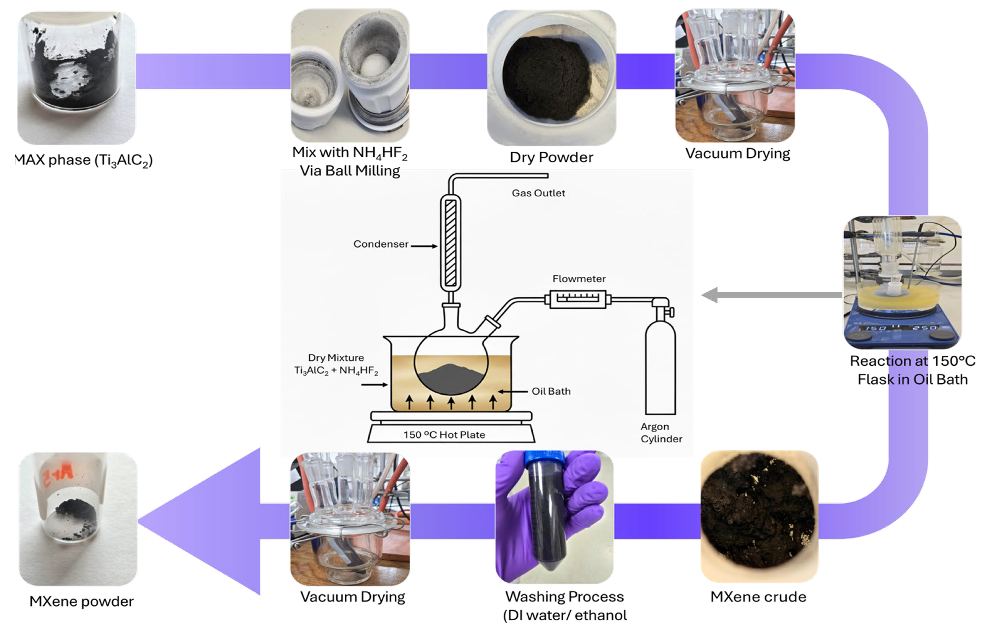
Figure 2.
(a) XRD patterns of Ti₃AlC₂ MAX phase (black) and Ti₃C₂Tₓ MXene (red). (b) Raman spectra of Ti₃AlC₂ (black) and Ti₃C₂Tₓ (red).
Figure 2.
(a) XRD patterns of Ti₃AlC₂ MAX phase (black) and Ti₃C₂Tₓ MXene (red). (b) Raman spectra of Ti₃AlC₂ (black) and Ti₃C₂Tₓ (red).
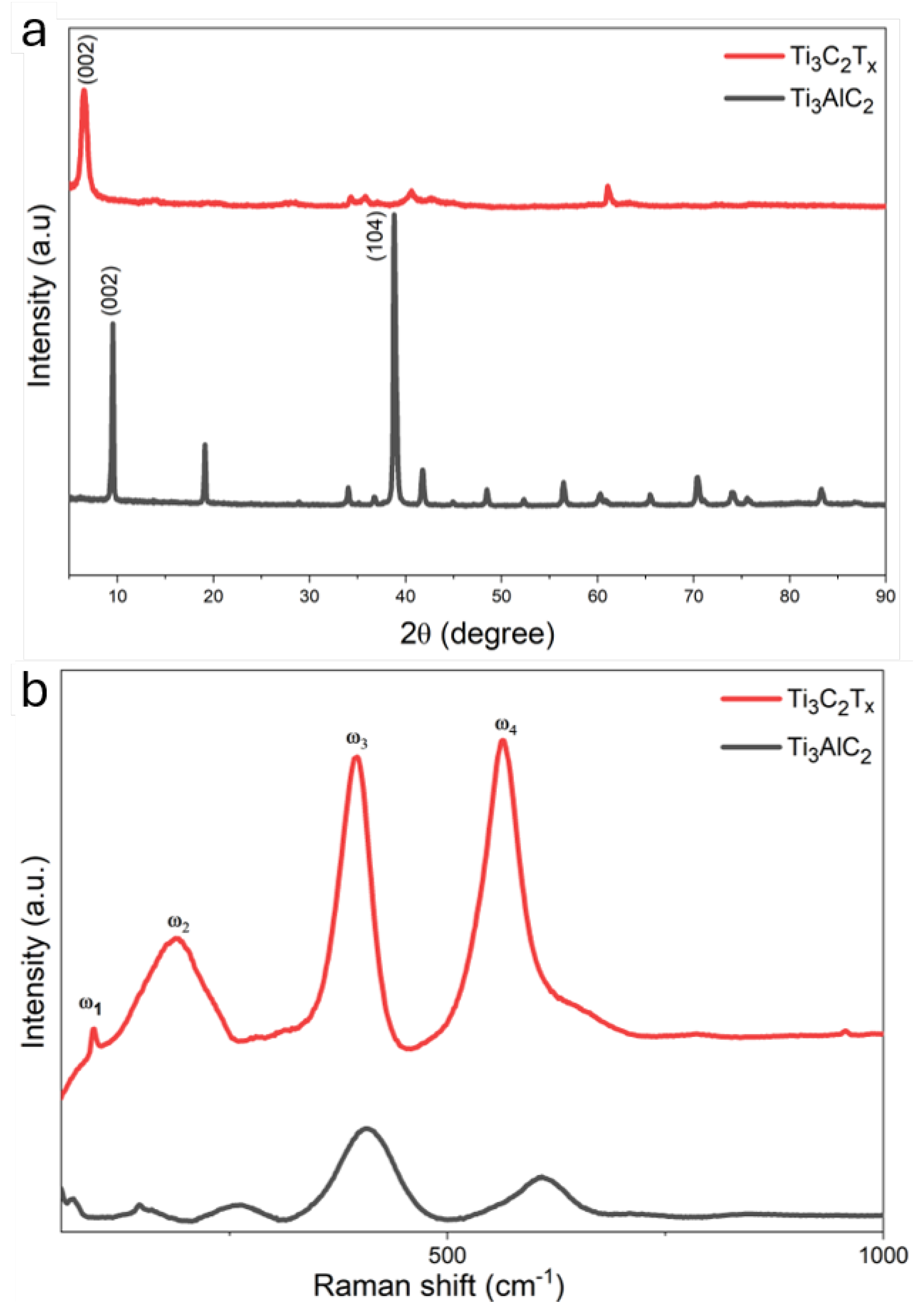
Figure 3.
(a) SEM image showing the exfoliated layered morphology of Ti3C2Tx sheets. (b) TEM image showing Ti3C2Tx single sheets (c) EDX elemental maps confirming the presence of Ti, C, O, and F surface terminations with no detectable Al.
Figure 3.
(a) SEM image showing the exfoliated layered morphology of Ti3C2Tx sheets. (b) TEM image showing Ti3C2Tx single sheets (c) EDX elemental maps confirming the presence of Ti, C, O, and F surface terminations with no detectable Al.
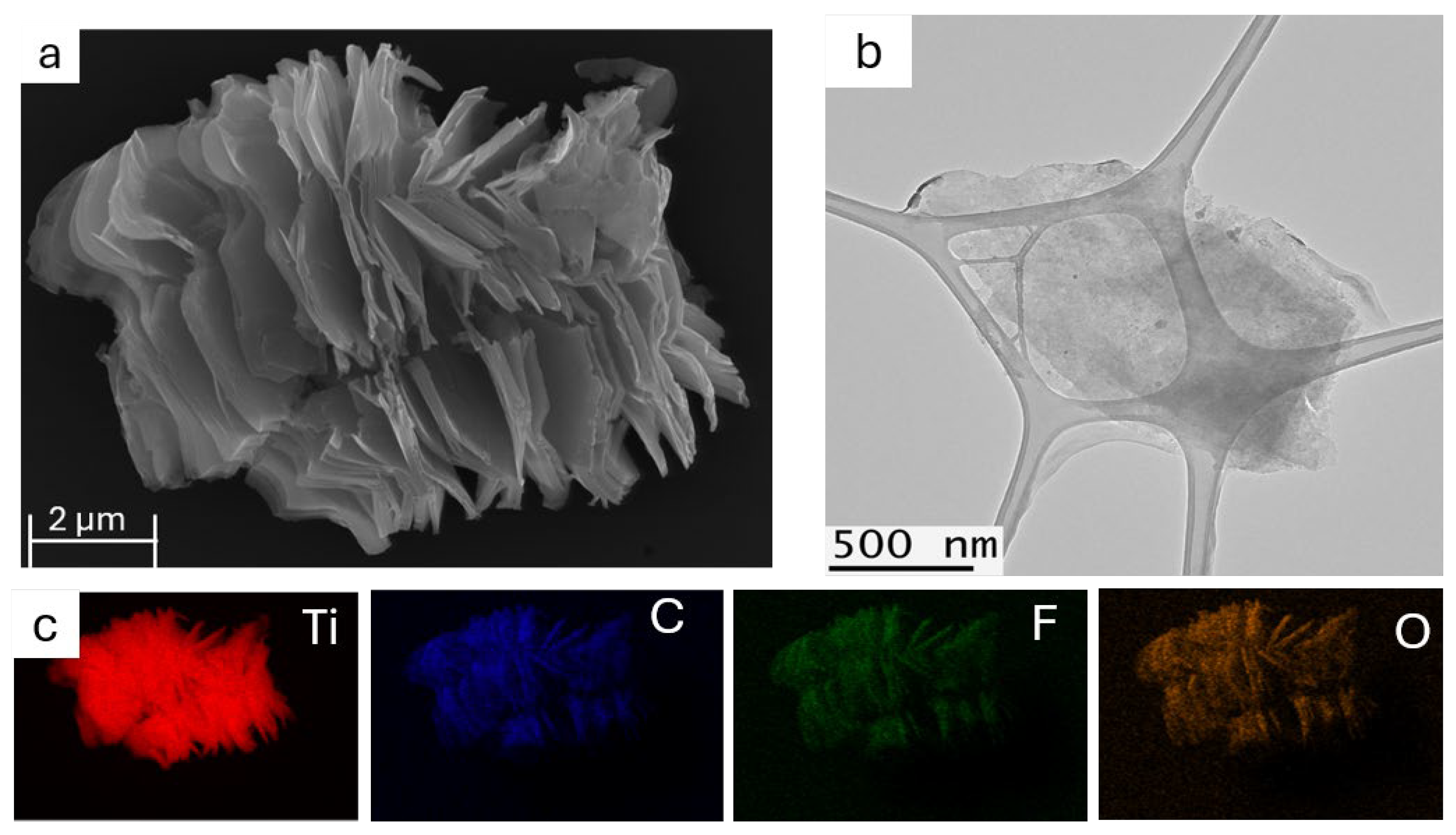
Figure 4.
Electrical characterisation of lateral and vertical Ti₃C₂Tₓ memristor devices. (a) I-V characteristics of the lateral memristor over -/+6 V with 100 cycles overlay. (b) I-V characteristics of the vertical Ag/Ti₃C₂Tₓ/Pt/Ti/Si memristor over ±6 V with 100-sweep overlay; inset shows resistance retention over 120 minutes.
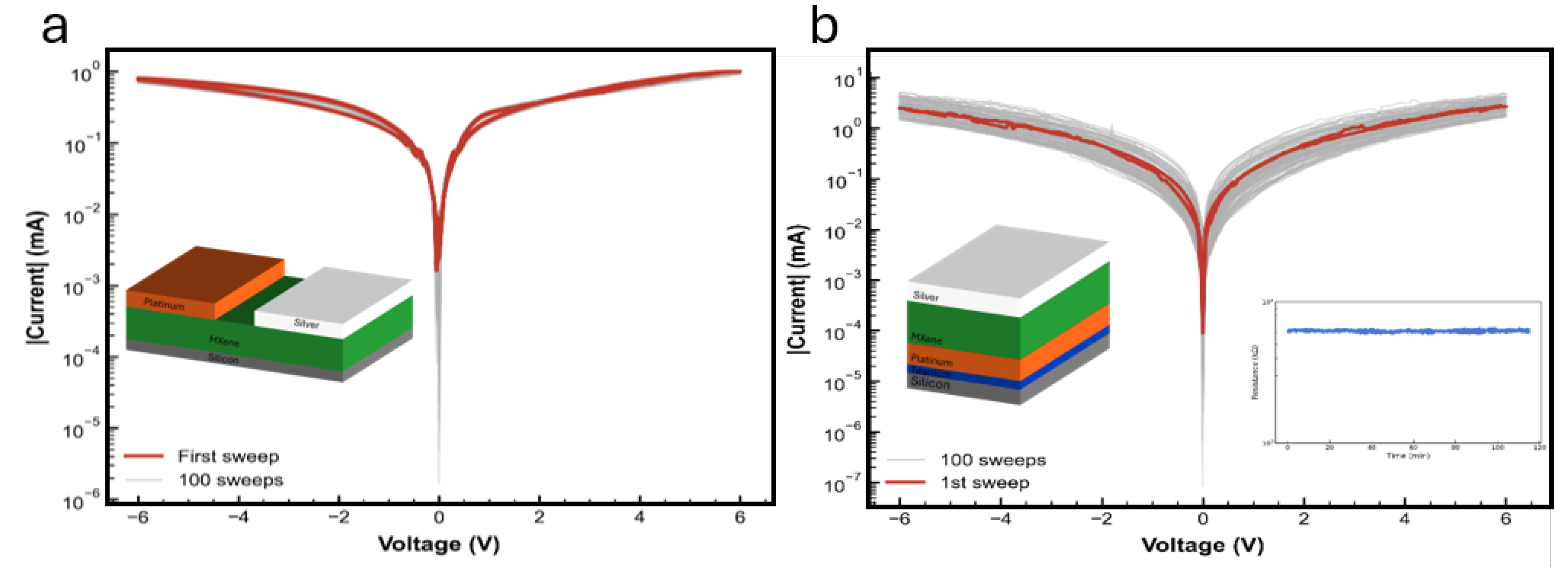
Figure 5.
Characterisation of UV-O₃-treated lateral Ti₃C₂Tₓ memristor. (a) Raman spectra of pristine (black) and UV-O₃-treated (red) Ti₃C₂Tₓ. (b) I-V characteristic of the UV-O₃-treated lateral memristor over ±8 V.
Figure 5.
Characterisation of UV-O₃-treated lateral Ti₃C₂Tₓ memristor. (a) Raman spectra of pristine (black) and UV-O₃-treated (red) Ti₃C₂Tₓ. (b) I-V characteristic of the UV-O₃-treated lateral memristor over ±8 V.
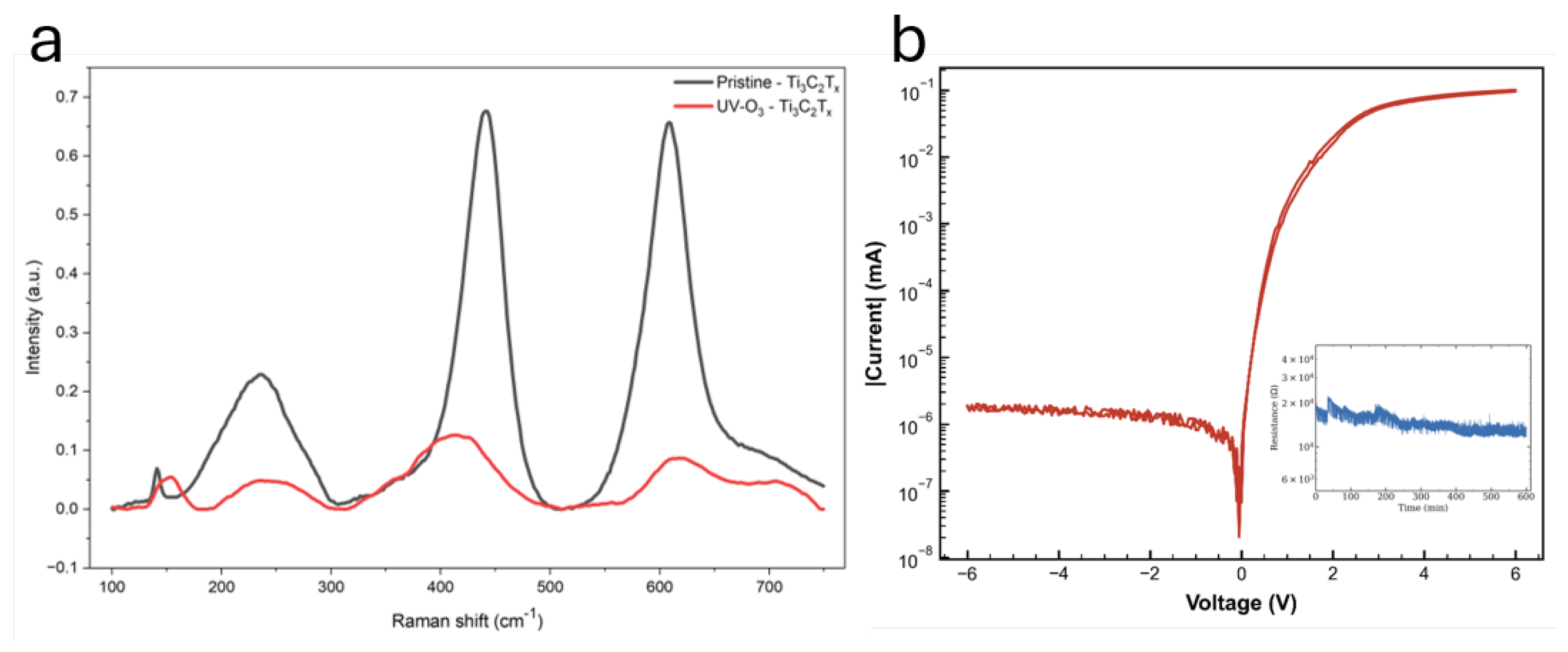

Table 1.
EDX Elemental composition of Ti3AlC2 MAX phase compared to Ti3C2Tx MXene.
| Sample | Ti (%) | Al (%) | C (%) | O (%) | F (%) |
|---|---|---|---|---|---|
| Ti3AlC2 (MAX) |
58.07 | 11.37 | 30.56 | - | - |
| Ti3C2Tx (MXene) |
43.90 | 0.00 | 26.34 | 15.63 | 14.13 |
Disclaimer/Publisher’s Note: The statements, opinions and data contained in all publications are solely those of the individual author(s) and contributor(s) and not of MDPI and/or the editor(s). MDPI and/or the editor(s) disclaim responsibility for any injury to people or property resulting from any ideas, methods, instructions or products referred to in the content. |
© 2026 by the authors. Licensee MDPI, Basel, Switzerland. This article is an open access article distributed under the terms and conditions of the Creative Commons Attribution (CC BY) license (http://creativecommons.org/licenses/by/4.0/).
Copyright: This open access article is published under a Creative Commons CC BY 4.0 license, which permit the free download, distribution, and reuse, provided that the author and preprint are cited in any reuse.