
Submitted:
28 August 2026
Posted:
01 September 2026
You are already at the latest version
Abstract
In this study, CdTe thin films were fabricated on soda-lime glass substrates via pulsed laser deposition and evaluated as immobilized semiconductor photocatalysts for the degradation of methylene blue under visible-light irradiation. XRD, AFM, SEM-EDS, photoluminescence, and photophysical characterization techniques were employed to elucidate the relationship between photocatalytic response and the structural, morphological, elemental, and optical characteristics of the fabricated thin films. Results show that increasing film thickness improves crystallinity, surface roughness, stoichiometry, optical absorption, and charge-carrier dynamics, while reducing the optical band gap from 1.71 to 1.37 eV. Among the fabricated samples, the 350 nm-thick CdTe film exhibited the highest photocatalytic performance, achieving 93.32% MB degradation after 220 minutes of visible-light irradiation, following pseudo-first-order kinetics with a rate constant of 0.0118 min⁻¹. Photocatalytic performance was strongly influenced by solution pH, with optimal degradation at pH 10. Furthermore, scavenger experiments demonstrated that reactive oxygen species, particularly superoxide radicals, played a dominant role in the overall degradation mechanism. These findings highlight CdTe thin films produced by PLD as promising immobilized photocatalysts for efficient wastewater treatment.
Keywords:
CdTe thin films
; pulsed laser deposition
; photocatalysis
; methylene blue degradation
; wastewater treatment
1. Introduction
Water pollution remains one of the most persistent environmental problems, especially due to synthetic organic contaminants associated with industrial activity, urbanization, and increasing freshwater demand [1]. Among these contaminants, synthetic dyes are particularly challenging in wastewater systems because even low dye concentrations can cause harmful effects, including intense coloration, reduced light penetration in aquatic environments, and disruption of biological balance. Also, industrial wastewater contaminated with dyes, pharmaceuticals, and other industrial contaminants is a crucial problem [2]. Accordingly, the design and optimization of experimental methods, theoretical models, and treatment systems are essential for improving strategies to mitigate water pollution.
With the rapid development of advanced oxidation and photo-assisted treatment technologies in recent decades, photocatalysis has attracted remarkable attention as an oxidation process driven by light, for the organic pollutant degradation under relatively mild conditions [2]. In a typical semiconductor photocatalytic process, incident photons with energy greater than or equal to the material’s band gap excite electrons from the valence band to the conduction band, leaving photogenerated holes. Subsequently, these charge carriers may migrate to the surface and participate in oxidation and reduction reactions with adsorbed water, hydroxide ions, oxygen, and pollutant molecules. Through these pathways, reactive oxygen species can be formed [3]. Therefore, the overall degradation efficiency depends not only on the optical absorption ability of the photocatalyst production, but also on the separation, migration, and lifetime of photo-generated electron-hole pairs[4].
Powder photocatalysts have been widely investigated [4]. Thin-film materials offer a practically important alternative as photocatalysts because the active material is immobilized on a solid substrate. This approach can limit catalyst loss during recovery and simplify post-treatment separations compared with those using suspended photocatalyst particles. Moreover, thin film photocatalysis provides its own designing opportunities (and challenges), since the photocatalytic response becomes highly sensitive to film thickness, crystallinity, surface roughness, grain structure, optical penetration depth, charge transfer behavior across the film or substrate interface, and all other physical features emerged after the manufacturing [5]. Therefore, the development of efficient thin-film photocatalysts requires careful correlation among deposition parameters, structural and morphological evolution, optical response, and photocatalytic activity and decolorization efficiency.
Most photocatalytic wastewater studies still focus on heavy oxide materials, especially TiO₂ and its modified derivatives [6]. Even though these systems are chemically stable and widely studied, their activity is often limited by insufficient visible-light utilization, charge-and-carrier recombination, and practical scaling-up difficulties. For this reason, there is a growing interest in alternative semiconductor thin films to find intrinsic optical and electronic properties that can support stronger light absorption and relatively more charge generation[7]. Chalcogenide semiconductors are especially attractive in this context because their band structures can be favorable for absorption in the visible region and for photoinduced charge transport. Recent thin-film studies employing calcogenides have shown that photocatalytic degradation of methylene blue (MB) is influenced by film composition, optical band gap, pH, and scavenger charge-transfer pathways. This emphasizes the importance of structure-property analysis in thin-film photocatalysis.
Cadmium telluride (CdTe) is a II–VI compound semiconductor material; commonly known for its direct band gap, high absorption coefficient, and strong optoelectronic functionality [8]. In a photocatalytic process, these same features make CdTe a promising material, since photocatalytic degradation itself is also governed by light absorption, electron–hole pair formation/lifetime, carrier transport mechanism, and surface redox reactions. Although CdTe has been widely studied for optoelectronic devices, its applications as an immobilized thin film have been less explored and have received relatively little attention. In particular, the relationship between its photocatalytic performance and the thin film’s structural, morphological, optical, and electrical properties has not been examined extensively.
On the other hand, the deposition technique is another essential decisive factor in determining the overall functional properties of CdTe thin films [9]. Pulsed laser deposition (PLD) is particularly well-suited for this purpose because it enables controlled material transfer from the target to the substrate. Also, PLD allows the thickness and surface morphology of the deposited film to be tuned by laser parameters, such as pulse number, laser energy, repetition rate, and deposition duration [10]. In our previous work on PLD-grown CdTe films, it has been shown that increasing the laser pulse number from 2400 to 9600 produced films with thicknesses from 185 to 437 nm, accompanied by systematic changes in crystallinity, surface morphology, stoichiometry, optical absorption, and band gap behavior of the overall system [11]. Thus, these results indicate that CdTe thin films produced by the PLD technique provide a tunable material system in which optical absorption, microstructure, and charge-carrier behavior can be adjusted by designing the deposition process.
In the present study, CdTe thin films produced by PLD on soda-lime glass (SLG) substrates were investigated as photocatalytic materials for MB degradation under visible and UV irradiation. Four CdTe thin-film designs with varying numbers of deposition pulses and corresponding thicknesses were first evaluated to assess the influence of film-growth conditions on photocatalytic performance. The photocatalytic process was monitored by collecting samples as solution aliquots at defined time intervals and analyzing the temporal evolution of MB absorbance using UV-Vis spectrophotometry. After identifying the most effective CdTe film design, additional photocatalytic experiments were performed under different additive and control conditions, including alkaline, acidic, additive-free, and scavenger conditions, to clarify the contributions of surface reactions and charge-transfer pathways to the overall degradation behavior.
The main purpose of this work is therefore not limited to demonstrating MB degradation using CdTe thin films, but also to establish a direct relationship between photocatalytic activity and the material properties produced by PLD growth. Using these methodologies and this context, this study aims to elucidate how CdTe film thickness, surface morphology, light absorption, and charge-transfer behavior govern the overall degradation process. In that way, as a more stable, immobilized opportunity, the work provides a much broader understanding of how thin-film design in semiconductors relates to photocatalytic performance in water-treatment applications.
2. Experimental
CdTe thin films were deposited on SLG substrates. The PLD technique was employed at room temperature using a 99.99% pure CdTe sputtering target, as shown in Figure 1. The target was ablated with laser pulses at 1064 nm. The laser had a pulse energy of 20 mJ, a 5 ns pulse duration, and a 10 Hz repetition rate. The distance between the target and the substrate was maintained at 52 mm throughout the deposition process. Before thin-film deposition, the vacuum chamber was evacuated to an approximate base pressure of 2 × 10⁻⁶ mbar to reduce contamination and to properly grow and align the plasma for depositing high-quality CdTe thin films. CdTe1, CdTe2, CdTe3, and CdTe4 thin-film samples with different thicknesses were obtained by varying the number of laser pulses (2400, 4800, 7200, and 9600) during ablation of the target CdTe material. Following the deposition, all samples were exposed to the annealing process at 500 °C temperature in a quartz tube furnace under vacuum conditions, as illustrated in Figure 1. The measured thicknesses of the CdTe1, CdTe2, CdTe3, and CdTe4 thin films were 185, 298, 350, and 437 nm, respectively. CdTe Thin films are shown in Figure 1a. CdTe thin films were comprehensively characterized in terms of their optical, crystalline, morphological, and elemental properties using UV-Vis spectroscopy, XRD, AFM, SEM, EDX and PL measurements were performed using a Renishaw inVia confocal Raman microscope with an excitation wavelength of 532 nm and a laser power of 5 mW.
The photocatalytic degradation of MB over CdTe thin-film photocatalysts was investigated under visible-light irradiation. Initially, 100 mL of MB aqueous solution was placed in a reaction vessel mounted on a magnetic stirrer to ensure continuous mixing throughout the experiment, as illustrated in Figure 1b. Each CdTe thin-film sample was immersed in 100 mL of MB solution and stirred under dark conditions for 20 min to attain adsorption–desorption equilibrium. Thereafter, a solution aliquot was withdrawn with a syringe and transferred into an Eppendorf tube for characterization. The photocatalytic degradation process was subsequently performed under visible-light irradiation from a 250 W metal-halide lamp (GE ARC250). During irradiation, solution aliquots were collected every 20 min until a total reaction time of 220 min. The absorption spectra of the MB aliquots collected in Eppendorf tubes were measured using a UV–Vis spectrophotometer.
3. Discussion
3.1. XRD Properties of CdTe Thin Films
The XRD patterns of the CdTe thin films in Figure 2 confirm the formation of a polycrystalline structure, where diffraction peaks corresponding to both cubic zinc blende (C) and the hexagonal (H) CdTe phases are observed. The strongest diffraction peak of the CdTe-1 ultrathin film appears at 2θ = 27.40°, corresponding to the (200)C plane, which is attributed to the preferential formation of this orientation owing to its relatively low crystallization energy. The diffraction peaks indexed to the overlapping (111)C/(002)H and (220)C/(110)H crystallographic planes at 2θ = 23.60° and 39.26°, respectively, exhibit the highest intensities in the CdTe3 and CdTe4 thin films [12,13]. The diffraction peak appearing at 2θ = 43.76° in all thin films is indexed to the (103) crystallographic plane of the hexagonal CdTe phase [14], whereas the peak located at 2θ = 46.40° is attributed to the (311) plane of the cubic phase. A diffraction peak appearing at 2θ = 38.16° is detected in the CdTe-1, CdTe-2, and CdTe-3 thin films and is assigned to the (102) crystallographic orientation of hexagonal Te [15]. The diffraction feature at 2θ = 50.9° (#) is most likely associated with elemental Te, consistent with previous studies, indicating that excess Te remained in the CdTe thin films after deposition [15,16].
3.2. Morphologic Properties of CdTe Thin Films
According to the AFM observations in Figure 3, increasing the number of laser pulses leads to the formation of larger particles. Based on the AFM results, the average roughness was measured as 6.66 nm for CdTe1, 10.69 nm for CdTe2, 12.58 nm for CdTe3, and 15.69 nm for CdTe4. Accordingly, the surface gradually became rougher as the number of pulses increased. This behavior may be related to the greater accumulation of adatoms on the substrate, which promotes grain growth and results in a less smooth film surface.
The crystallite sizes of the CdTe4, CdTe3, CdTe2, and CdTe1 samples were calculated as 48.54 nm, 49.63 nm, 47.37 nm, and 44.46 nm, respectively. The calculation was performed by using the Scherrer equation.
Figure 4a shows that the CdTe1 thin film exhibits a morphology of small particles, reflecting the relatively low amount of deposited material due to the low number of laser pulses [17]. The increased deposition of ablated species leads to a denser and more continuous particle distribution in the CdTe2 and CdTe3 thin films, as evidenced by the SEM images in Figure 4b and Figure 4c. The CdTe4 thin film deposited at 9600 laser pulses exhibits pronounced particle coalescence, resulting in the formation of island-like morphologies, as shown in Figure 4d. This behavior arises from the increased accumulation of ablated species and the enhanced grain growth at higher deposition levels.
EDX characterization in Figure 5 reveals that CdTe1, CdTe2, and CdTe3 thin films possess a tellurium-rich composition. An excess of Te favors the formation of Cd vacancies (VCd) [18] which can subsequently be occupied by Te atoms, resulting in TeCd antisite defects acting as deep native donor defects. Cd/Te values of CdTe1, CdTe2, CdTe3 ad CdTe4 thin films are 0.75, 0.81, 0.86, 1.11, respectively. As the number of laser pulses increases, the reduction in Te content shifts the Cd/Te ratio toward unity, resulting in a more stoichiometric CdTe4 thin film. The reduction in the intensity of the Te diffraction peaks with increasing film thickness, as observed in the XRD patterns, further supports this conclusion.
3.3. Optical Properties of CdTe Thin Films
Figure 6a shows that the CdTe4 thin film has the highest absorption property in the near infrared region owing to its large island textured morphology. By comparison, the CdTe1 thin film consists of relatively small particles and exhibits weaker absorption, with reduced absorption near 1200 nm. CdTe3 and CdTe4 thin films exhibit enhanced absorbance in both the short-wavelength and near-infrared regions as a result of increased film thickness, improved crystallinity, and better stoichiometric composition.
The optical band gap energies () were obtained by using the linear sections of the Tauc plots given in Figure 6b and extending them toward the photon energy axis, according to the following equation [19]:
where represents the measured optical absorbance, while denotes the photon energy. The band gaps of CdTe4, CdTe3, CdTe2, and CdTe1 thin films were determined as 1.37 eV, 1.50 eV, 1.59 eV, and 1.71 eV, respectively. The observed redshift in the absorption spectra indicates a reduction in the optical band gap of the thin films. The combination of increased light absorption and a reduced band gap enhances the generation of electron-hole pairs under illumination, thereby favoring photocatalytic reactions.
Figure 6c illustrates the PL spectra of the thin films, which exhibit a distinct emission peak located at 771 nm. The thinner CdTe1 film was characterized by lower crystallinity, which is associated with an increased density of grain-boundary-defects and trap states that act as recombination centers. With increasing film thickness, larger grains form, reducing the number of grain boundaries and suppressing the density of defect-related trap states. Increasing the film thickness promotes compositional uniformity by reducing Cd deficiency and excess Te, thereby driving the CdTe films toward stoichiometric composition. This improvement can reduce the likelihood of forming deep-level defects caused by Te, such as Te interstitials and antisites, thereby increasing the minority-carrier lifetime by suppressing defect-induced recombination. The higher PL emission at 771 nm observed for thicker CdTe films suggests more efficient photon recycling in the system, thereby increasing overall light harvesting and promoting photocatalytic performance.
3.4. Photodegradation Activity of MB Dye for CdTe Thin Film Catalyst
In this work, the catalytic effect of CdTe thin films on MB dye removal was investigated. The degradation percentage of MB was calculated according to the following expression[20]:
where C₀ denotes the initial MB concentration, and Ct represents the concentration measured after a radiation time of . The photocatalytic degradation performance of MB was systematically assessed using CdTe1 (185 nm), CdTe2 (298 nm), CdTe3 (350 nm), and CdTe4 (437 nm) ultrathin films, each with varying thicknesses, coated onto glass substrates. Before illumination, the photocatalyst and MB solution were allowed to equilibrate in the dark for 20 min to establish adsorption-desorption equilibrium. No measurable decrease in the MB concentration was detected before light irradiation. The results confirm that the adsorption of MB on the CdTe thin films is negligible[21]. Additionally, to evaluate the direct photolysis of MB, the dye solution was irradiated under visible light in the absence of the photocatalyst. Observing only 4.94% degradation after 220 min indicates that self-photodegradation was insignificant, as shown in Figure 7a.
The photocatalytic removal efficiencies of MB dye were determined as 84.19%, 89.48%, 93.32% and 90.76% with the samples of CdTe1, CdTe2, CdTe3 and CdTe4 thin film catalysts, respectively, as it can be seen in Figure 7a. Photocatalytic experimental sessions that are employing CdTe thin films of various thicknesses demonstrated that the degradation efficiency reached its maximum at a film thickness of 350 nm, followed by a slight decrease upon further increasing the thickness to 437 nm, unexpectedly but reasonably. The increase in crystallite size and the enhanced crystalline quality, accompanied by a reduction in grain-boundary density, facilitate efficient charge transport by suppressing recombination. An increase in film thickness improves optical absorption, thereby generating more photogenerated electron–hole pairs [22]. However, when the CdTe4 catalyst thickness was increased to 437 nm, the catalytic efficiency decreased slightly. This is because: i) Since sufficient light cannot diffuse into the substrate region of the thin film, e-h pair formation remains limited. ii) Photo-excited charge carriers formed within the thin film may not reach the surface and may not interact with the molecular structure of the MB dye solution. iii) Water, dissolved oxygen, and dye molecules may have more difficulty reaching the active sites, thus reducing the rate of surface reactions[23].
To elucidate the effect of film thickness on photocatalytic performance, the degradation kinetics were fitted using the model of Langmuir-Hinshelwood pseudo-first order [21]. Under the same photocatalytic conditions (pH = 10), but in the removal of a catalyst, the reaction rate constant for MB degradation was found to be only 0.0002 min⁻¹. The maximum photocatalytic degradation rate was achieved using the CdTe thin film of 350 nm thickness, for which the apparent first-order kinetic constant was determined to be 0.0118 min⁻¹. The corresponding kinetic constants for CdTe thin films at 185nm, 298nm, and 437 nm-thickness were 0.0083, 0.0101, and 0.0112 min⁻¹, respectively. The UV–Vis absorption spectra presented in Figure 7c reveal that the characteristic absorption peak of MB at approximately 664 nm gradually diminished under visible-light irradiation and became nearly undetectable at the end of the photocatalytic process. The gradual loss of the characteristic MB absorption peak confirms the remarkable photocatalytic degradation of the dye under visible-light irradiation in the presence of the CdTe thin-film photocatalyst, accompanied by its conversion into less complex degradation products.
The photocatalytic oxidation mechanism responsible for the decomposition of MB dye in the presence of the CdTe semiconductor is represented by the following equations: (3–8) [24]:
To understand the proposed mechanism, a conceptual schematic diagram illustrating the photocatalytic degradation process of organic dyes under visible light irradiation with the CdTe thin-film photocatalyst is provided in Figure 7d. The photocatalytic mechanism of the CdTe thin-films can be defimed as the photons with equal or greater energies than the band gap of the CdTe semiconductor is absorbed by the film, therefore promoting the formation of photo-induced e⁻–h⁺ pairs (in Eq. 3). The photo-induced electron and hole pairs either recombine, resulting in energy loss, or are effectively separated and transferred to the photocatalyst surface, where they initiate oxidation–reduction reactions. The photo-generated holes (h⁺) accumulated in the valence band oxidize surface-adsorbed water molecules, which is resulting in the formation of notably reactive hydroxyl radicals (*OH), as expressed in Eq. (4) and Eq. (5)[25]. The photo-generated electrons in the conduction band are transferred to adsorbed oxygen molecules on the photocatalyst surface, resulting in the formation of superoxide radical anions (•O₂⁻), as illustrated in Eq. (6). •O₂⁻ generated on the photocatalyst surface further reacts with water molecules, producing hydrogen peroxide (H₂O₂), which subsequently yields *OH, as illustrated in Eqs. (6) and (7). These highly oxidative •OH radicals are the primary reactive oxygen species, which are responsible for the efficient degradation of organic dye molecules [25,26]. The complete photocatalytic reaction pathway discussed above is illustrated schematically in the energy band diagram of the CdTe thin-film photocatalyst, as shown in Figure 7d.
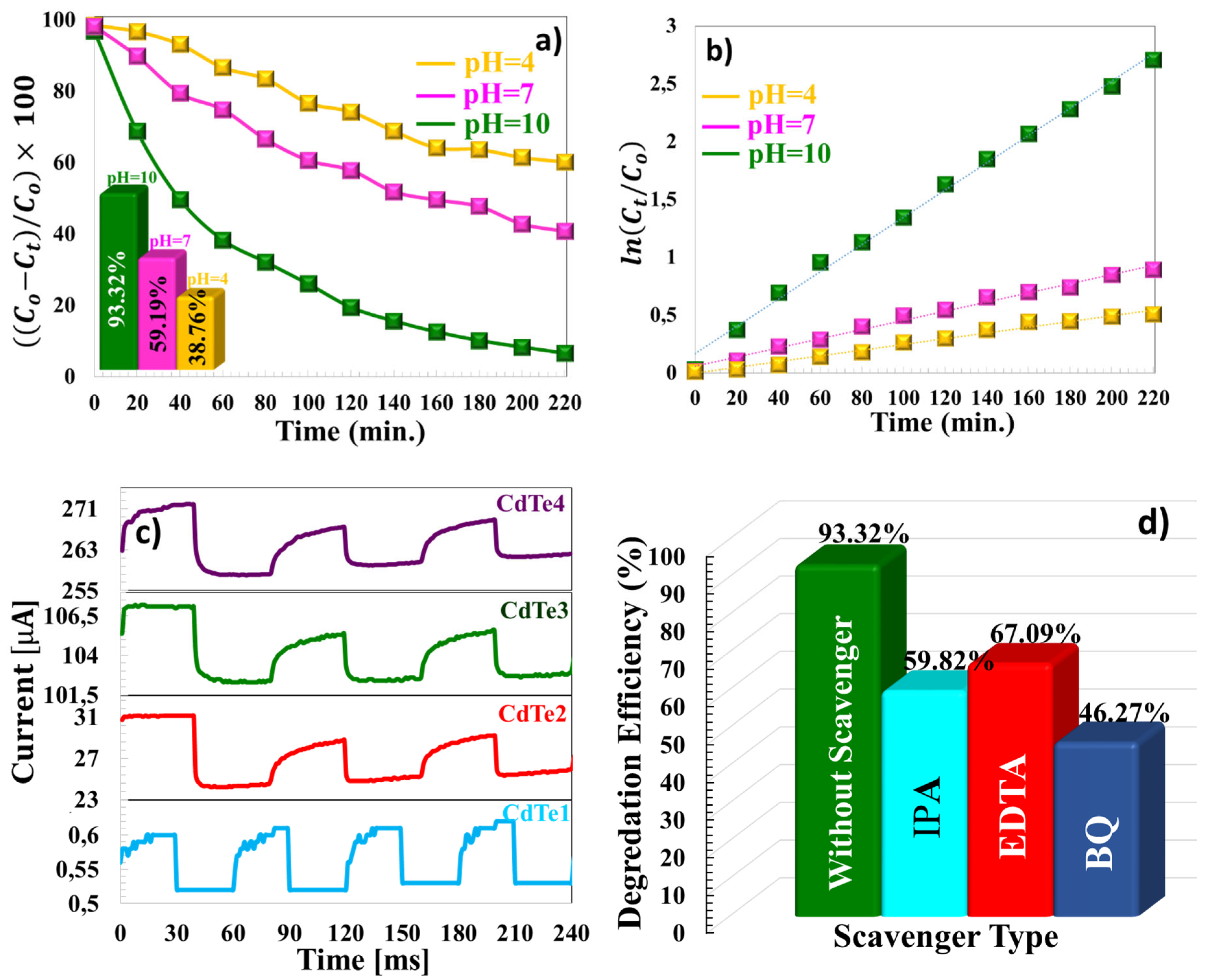
The photocatalytic degradation of organic dyes is strongly dependent on solution pH; additionally, pH determines both the adsorption dynamics and the surface charge characteristics of the photocatalyst thin film. Accordingly, three pH values were employed in this study to investigate their effects on MB dye removal. The pH of the MB solution was carefully adjusted to 4.0 (acidic), 7.0 (neutral), and 10.0 (basic) using 0.1 M HCl (acidic) and 0.1 M NaOH (basic) before the photocatalytic degradation tests. In the acidic environment (pH=4), the surface of the CdTe thin film becomes positively charged due to the high H⁺ ion concentration. Since MB dye is a cationic dye in aqueous solution, the electrostatic repulsion force between the CdTe surface and MB molecules reduces the adsorption of MB molecules to the catalyst surface and limits contact with the active sites[27]. Furthermore, the low concentration of OH⁻ ions reduces the formation of •OH radicals, resulting in the lowest possible photocatalytic degradation efficiency of 39.76% in Figure 8a. At neutral pH (7), the net electric charge on the CdTe surface decreases to zero. Therefore, the electrostatic effect, a repulsion between the MB molecules and the catalyst surface, is largely eliminated, allowing MB molecules to be adsorbed onto the surface more easily, and photocatalytic reactions occur more efficiently [28]. Thus, the photodegradation efficiency of 59.19% is significantly higher than in an acidic environment. In a cationic environment, the surface of the CdTe thin film becomes negatively charged due to the adsorbed OH⁻ ions. Since MB molecules are positively charged, a strong electrostatic attraction develops between the CdTe surface and MB, promoting greater adsorption of MB molecules onto the catalyst surface and enhancing the reaction at the active sites. Due to strong surface adsorption, efficient charge transfer, and high production of reactive oxygen species, the highest photocatalytic degradation efficiency of 93.32% is achieved at pH = 10. The kinetic constants for pH4, pH7, and pH10, which have been calculated to be 0.0028 min-1, 0.0045 min-1, and 0.0118 min-1, respectively, as seen in Figure 8b.
The time-dependent photocurrent density curves of the CdTe photocatalysts recorded under periodic visible light irradiation (light on and off cycles) are presented in Figure 8c. The measurement of photocurrent outputs of the CdTe1, CdTe2, CdTe3, and CdTe4 thin film photocatalysts was 0.512, 28.192, 101.516, and 166.68 µA, respectively. They showed that increasing the film thickness led to improved crystallinity, thus improving light-harvesting ability. In addition, the higher PL emission intensity indicates us a longer lifetime of photo-generated minority charge carriers. To elucidate the photocatalytic degradation mechanism under visible light radiation, ethylenediaminetetraacetic acid disodium salt (EDTA-2Na5 mmol L⁻¹), isopropanol (IPA5 mmol L⁻¹), and p-benzoquinone (BQ1 mmol L⁻¹) were employed as selective scavengers for h⁺, •OH, and •O₂⁻, respectively, in the presence of the CdTe thin films photocatalyst [28,29,30]. The addition of the BQ scavenger significantly suppressed the photocatalytic degradation efficiency to 46.27%, demonstrating that •O₂⁻ radicals are the primary reactive species responsible for the degradation of MB, as illustrated in Figure 8d. Compared with •O₂⁻ radicals, photogenerated holes (h⁺) showed a relatively lower contribution to the photocatalytic degradation of MB. Upon the addition of the EDTA-2Na scavenger, the degradation efficiency decreased to 67.09%, confirming the involvement of h⁺ in the photocatalytic reaction. In the presence of IPA, the photodegradation efficiency decreased to 59.82%, suggesting that radicals make a relatively smaller contribution to the photocatalytic degradation process than h⁺ radicals.
4. Conclusions
CdTe thin films with thicknesses of 185, 298, 350, and 437 nm were successfully deposited on soda-lime glass substrates using pulsed laser deposition and evaluated as visible-light photocatalysts for methylene blue (MB) degradation. Increasing the number of laser pulses significantly improved the structural, optical, and photocatalytic properties of the films. Crystallite size increased from 44.46 to 49.63 nm, while surface roughness rose from 6.66 to 15.69 nm, indicating enhanced grain growth and surface development. EDX analysis revealed that the Cd/Te ratio increased from 0.75 to 1.11 as thickness increased, approaching stoichiometric composition.
Optical characterization showed that the band gap decreased from 1.71 to 1.37 eV (CdTe1 to CdTe4), accompanied by enhanced visible-light absorption and stronger PL emission at 771 nm, indicating improved photon harvesting and prolonged charge-carrier lifetime. These improvements directly enhanced photocatalytic performance. The 350 nm-thick CdTe3 film achieved the highest activity with 93.32% MB degradation under visible light irradiation and a pseudo-first-order rate constant of 0.0118 min⁻¹, compared to 84.19%, 89.48%, and 90.76% for CdTe1, CdTe2, and CdTe4, respectively. The slight decline in CdTe4 (437 nm) was attributed to limited light penetration, longer carrier diffusion pathways, and reduced access to active surface sites. Photocatalytic performance strongly depended on solution pH, with degradation efficiencies of 39.76%, 59.19%, and 93.32% at pH 4, 7, and 10, respectively (rate constants: 0.0028, 0.0045, and 0.0118 min⁻¹). Alkaline conditions significantly improved degradation by enhancing electrostatic interactions and increasing the generation of reactive oxygen species. Photocurrent measurements confirmed improved charge separation, with photocurrent densities increasing from 0.512 μA (CdTe1) to 166.68 μA (CdTe4) under visible light.
Data availability statement
Data will be made available on reasonable request.
Conflicts of Interest
All authors declare they have no conflicts of interest.
Consent to Participate
Not applicable.
Consent for Publication
Not applicable.
References
- Weng, X.; et al. Beyond isolated capacity values: A multivariant framework for the evaluation of urea adsorption performance. 2026. [Google Scholar]
- Khader, E.H. Recent advances in photocatalytic advanced oxidation processes for organic compound degradation: A review . Desalination and Water Treatment 2024, 318, 100384. [Google Scholar] [CrossRef]
- Paiu, M. Heterogeneous photocatalysis for advanced water treatment: materials, mechanisms, reactor configurations, and emerging applications. Applied Sciences 2025, 15(10), 5681. [Google Scholar] [CrossRef]
- Lee, D.-E. State-of-the-art review on photocatalysis for efficient wastewater treatment: Attractive approach in photocatalyst design and parameters affecting the photocatalytic degradation. Catalysis Communications 2023, 183, 106764. [Google Scholar] [CrossRef]
- Dundar, I.; et al. Thickness effect on photocatalytic activity of TiO2 thin films fabricated by ultrasonic spray pyrolysi. Catalysts 2020, 10(9), 1058. [Google Scholar] [CrossRef]
- Chen, D.; et al. Photocatalytic degradation of organic pollutants using TiO2-based photocatalysts: A review. journal of cleaner production 2020, 268, 121725. [Google Scholar] [CrossRef]
- Šuligoj, A.; et al. Solar-driven photocatalytic films: synthesis approaches, factors affecting environmental activity, and characterization features. Topics in Current Chemistry 2022, 380(6), 51. [Google Scholar] [CrossRef] [PubMed]
- Bukhtiar, A.; Zou, B. Low-dimensional II–VI semiconductor nanostructures of ternary alloys and transition metal ion doping: synthesis, optical properties and application. Materials Advances 2024, 5(17), 6739–6795. [Google Scholar] [CrossRef]
- Romeo, A.; Artegiani, E. CdTe-based thin film solar cells: past, present and future. Energies 2021, 14(6), 1684. [Google Scholar] [CrossRef]
- Gezgin, S.Y.; Kepceoğlu, A.; Kılıç, H.Ş. An investigation of localised surface plasmon resonance (LSPR) of Ag nanoparticles produced by pulsed laser deposition (PLD) technique. In AIP Conference Proceedings; AIP Publishing LLC, 2017. [Google Scholar]
- Tuna, A. Photodetector properties of CdTe thin films and CdTe/Si heterojunctions produced by pulse laser ablation Optical and Quantum. Electronics 2026, 58(3), 126. [Google Scholar] [CrossRef]
- Adhikari, D.; et al. Glancing angle deposited CdTe: Nanostructured films and impact on solar cell performance Surface and Coatings. Technology 2020, 381, 125127. [Google Scholar] [CrossRef]
- Akbarnejad, E. Correlation between different CdTe nanostructures and the performances of solar cells based on CdTe/CdS heterojunction Journal of Electroanalytical. Chemistry 2019, 849, 113358. [Google Scholar] [CrossRef]
- Bindra, H.S. Controlled and selective growth of 1D and 3D CdTe nanostructures through a structurally engineered porous alumina template for enhanced optical application. Journal of The Electrochemical Society 2018, 165(4), H3061–H3068. [Google Scholar] [CrossRef]
- Hernandez-Vasquez, C. Influence of Te layer on CdTe thin films and their performance on CdS/CdTe solar cells. Superficies y vacío 2021, 34. [Google Scholar]
- Tang, G.; et al. Phosphate glass-clad tellurium semiconductor core optical fiber. Journal of Alloys and Compounds 2015, 633, 1–4. [Google Scholar] [CrossRef]
- Gezgin, S.Y. Modelling and investigation of the electrical properties of CIGS/n-Si heterojunction solar cell. Optical Materials 2022, 131, 112738. [Google Scholar] [CrossRef]
- Shepidchenko, A.; et al. Small hole polaron in CdTe: Cd-vacancy revisite. Scientific reports 2015, 5(1), 14509. [Google Scholar] [CrossRef] [PubMed]
- Kişnişci, Z.; et al. Optical characterization of Cu2ZnSnS4 nanocrystals thin film. Journal of Materials Science: Materials in Electronics 2016, 27(10), 10128–10135. [Google Scholar] [CrossRef]
- Olatunde, O.C.; Onwudiwe, D.C. Synth. Reduc. Graphene Oxide/copper Tin Sulfide (Cu2SnS3) composite for the photocatalytic degradation of tetracycline Journal of Inorganic and Organometallic. Polymers and Materials 2022, 32(7), 2578–2590. [Google Scholar]
- Gezgin, S.Y.; et al. Cu2Sn1− x Gd x S3 thin films for photocatalytic degradation of methylene blue. Nanoscale Advances 2025, 7(20), 6535–6550. [Google Scholar] [CrossRef] [PubMed]
- Hossain, R. Design, synthesis, and structural characterization of Fe2+-doped anatase TiO2 nanocrystals and its impact on electronic properties and photocatalytic activity. Materials Advances 2025. 6, 21, 7821–7836. [Google Scholar] [CrossRef]
- Zahoor, S. Advances in mesoporous nanomaterials for photocatalytic degradation of pollutants: fundamentals, material classifications, challenges and future prospect. Coordination Chemistry Reviews 2026, 217239. [Google Scholar]
- Maheskumar, V.; Vidhya, B. Investigation on the morphology and photocatalytic activity of Cu3SnS4 synthesized by ball milling and solvothermal metho. Journal of Photochemistry and Photobiology A: Chemistry 2018, 356, 521–529. [Google Scholar] [CrossRef]
- Wang, J. Photo-induced reactive oxygen species for selective oxidation of plastics and biomas. Journal of Photochemistry and Photobiology C: Photochemistry Reviews 2026, 100737. [Google Scholar]
- Abdullah, A.; et al. UV and visible light-driven production of hydroxyl radicals by reduced forms of N, F, and P codoped titanium dioxide. Molecules 2019, 24(11), 2147. [Google Scholar] [CrossRef] [PubMed]
- Hkiri, K. Experimental and theoretical insights into the adsorption mechanism of methylene blue on the (002) WO3. Surf. Sci. Rep. 2024, 14(1), 26991. [Google Scholar] [CrossRef] [PubMed]
- Khan, S.; et al. Photocatalytic degradation of organic dyes contaminated aqueous solution using binary CdTiO2 and ternary NiCdTiO2 nanocomposites. Catalysts 2022, 13(1), 44. [Google Scholar] [CrossRef]
- Pelaez, M.; et al. Use of selected scavengers for the determination of NF-TiO2 reactive oxygen species during the degradation of microcystin-LR under visible light irradiatio. Journal of Molecular Catalysis A: Chemical 2016, 425, 183–189. [Google Scholar] [CrossRef] [PubMed]
- Yao, S.; et al. Enhanced photocatalytic degradation of Rhodamine B by reduced graphene oxides wrapped-Cu2SnS3 flower-like architectures. Journal of Alloys and Compounds 2017, 704, 469–477. [Google Scholar] [CrossRef]
Figure 1.
a) Schematic illustration of the experimental procedure for the production of CdTe thin films and the photographs of the thin films and b) Schematic illustration of the photocatalytic degradation process of MB solution using CdTe thin-film photocatalysts.
Figure 1.
a) Schematic illustration of the experimental procedure for the production of CdTe thin films and the photographs of the thin films and b) Schematic illustration of the photocatalytic degradation process of MB solution using CdTe thin-film photocatalysts.
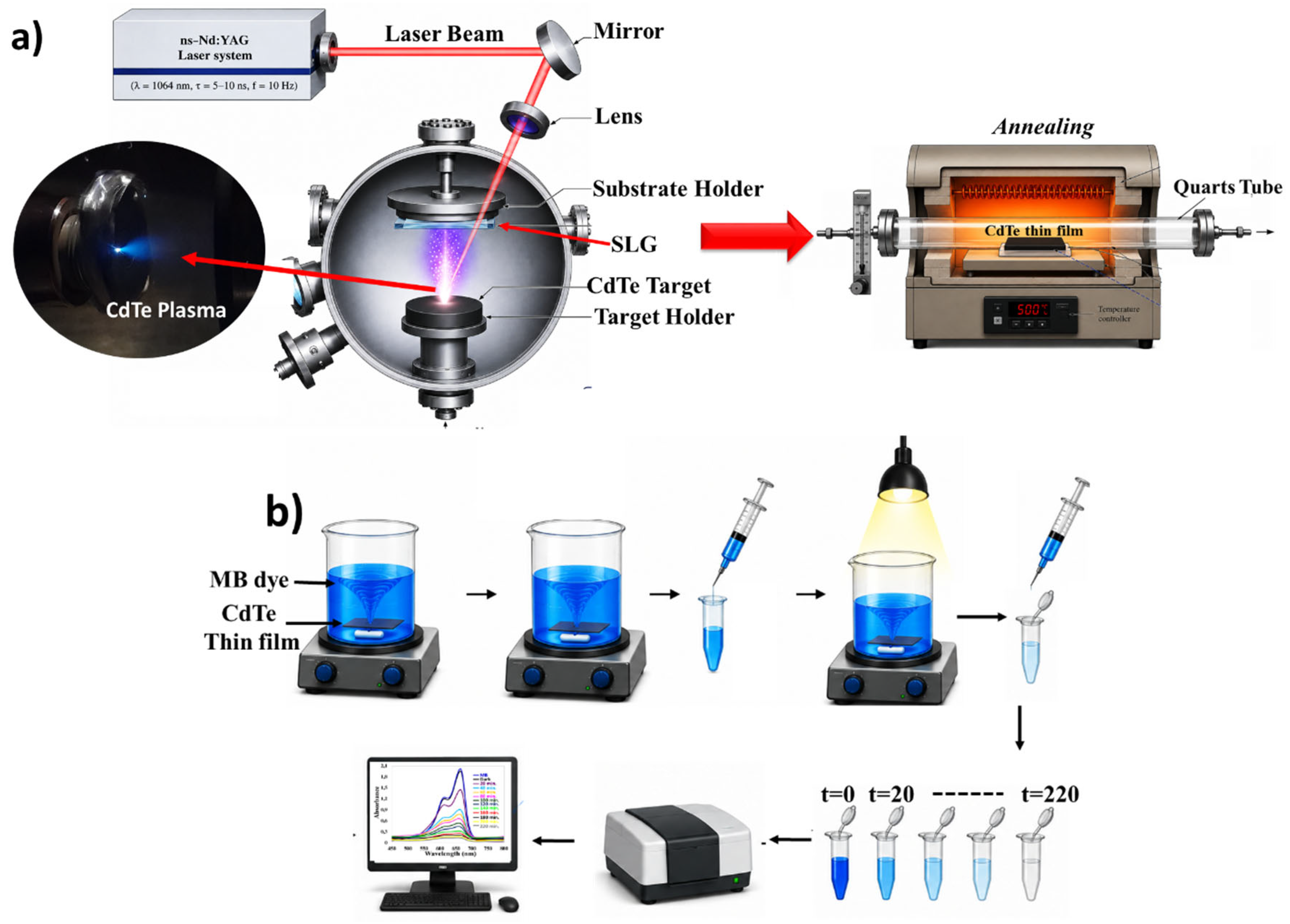
Figure 2.
X-ray diffraction patterns of the CdTe thin films.
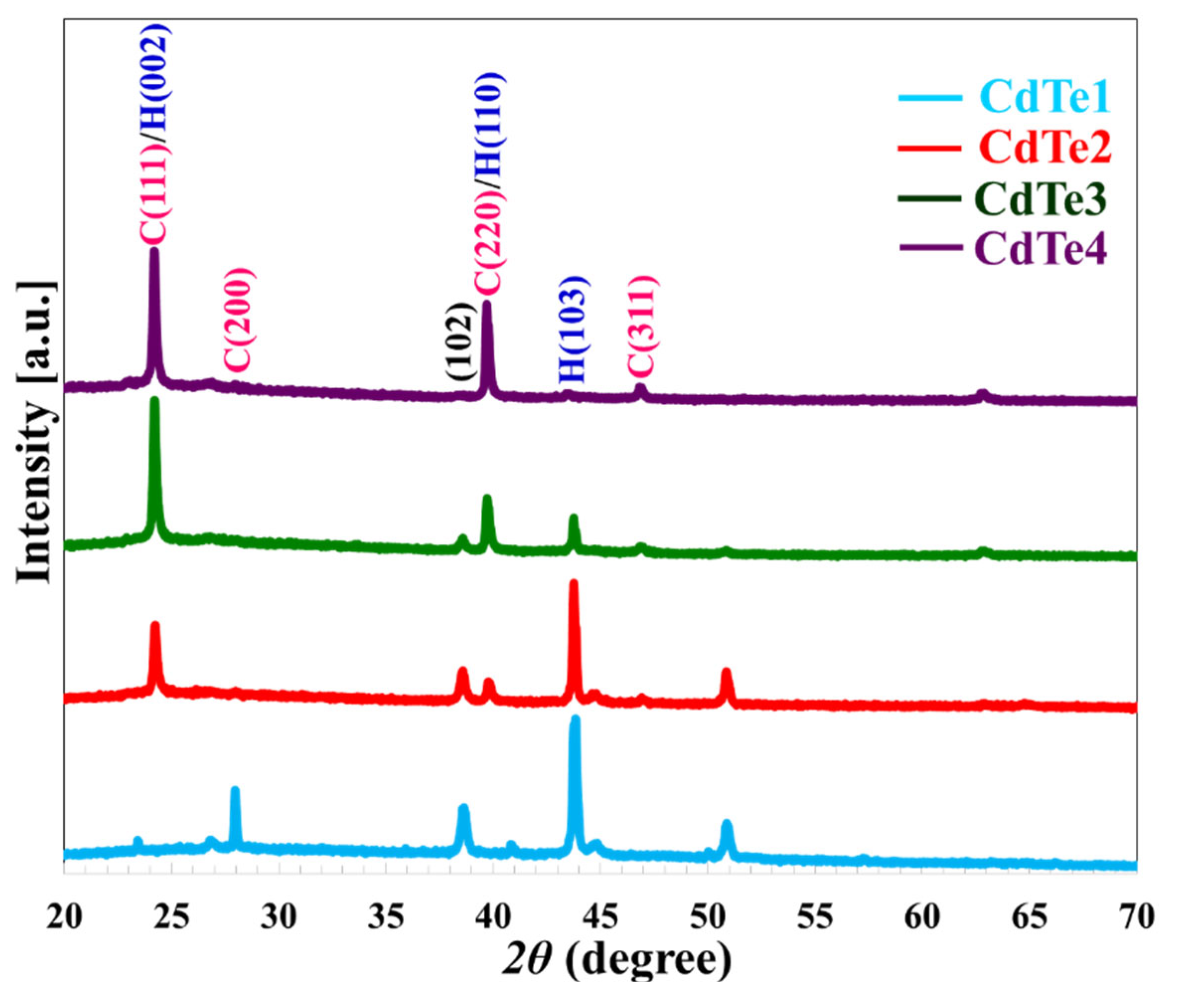
Figure 3.
Three-dimensional AFM topographical images (3 μm × 3 μm) of a) CdTe1, b) CdTe2, c) CdTe3, and d) CdTe4 thin films.
Figure 3.
Three-dimensional AFM topographical images (3 μm × 3 μm) of a) CdTe1, b) CdTe2, c) CdTe3, and d) CdTe4 thin films.
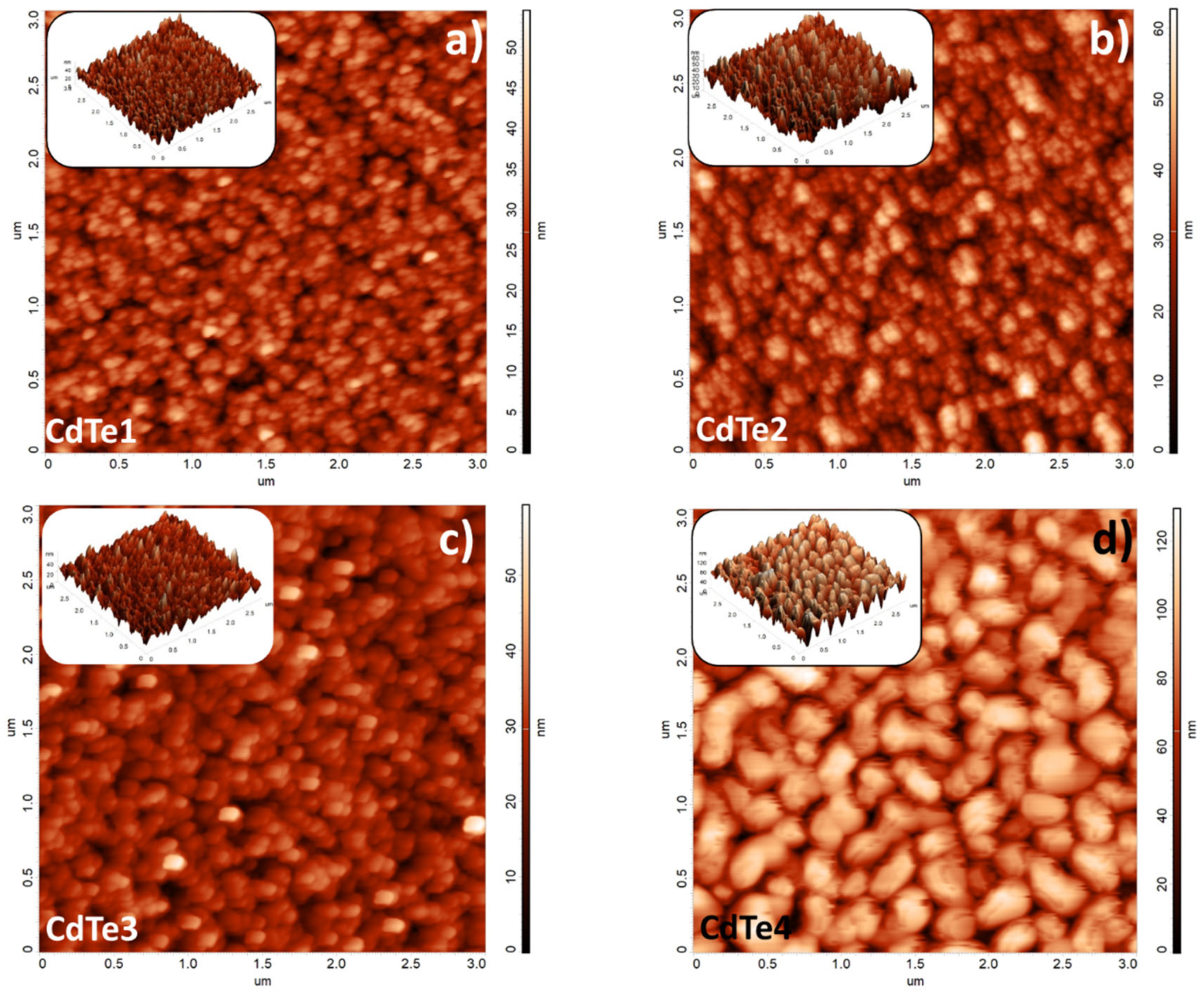
Figure 4.
Surface morphology of a) CdTe1, b) CdTe2, c) CdTe3, and d) CdTe4 thin films obtained by SEM analyses.
Figure 4.
Surface morphology of a) CdTe1, b) CdTe2, c) CdTe3, and d) CdTe4 thin films obtained by SEM analyses.
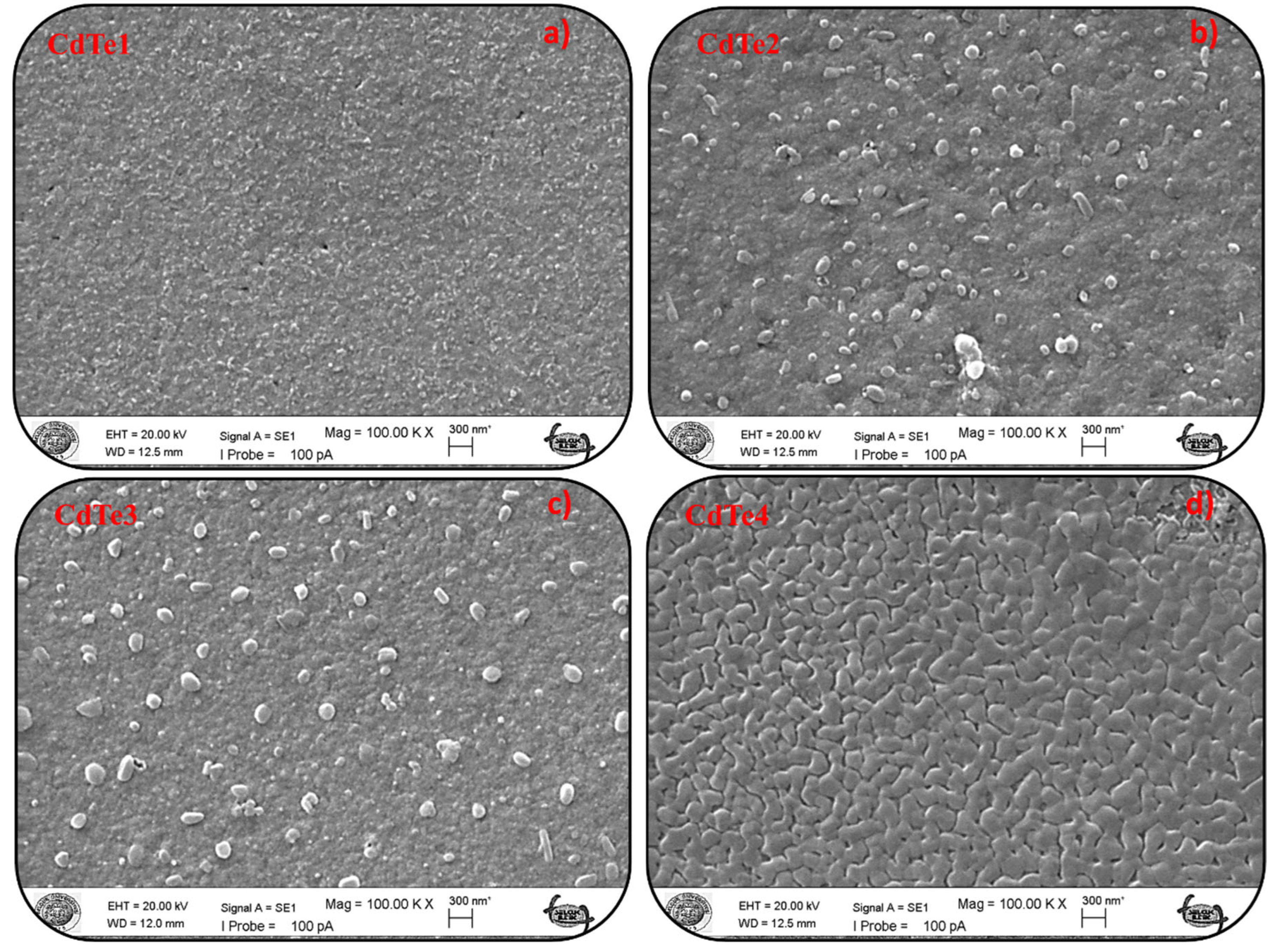
Figure 5.
EDX spectra together with corresponding elemental mapping images of a) CdTe1, b) CdTe2, c) CdTe3, and d) CdTe4 thin films. The elemental distributions are shown as Cd (red) and Te (green).
Figure 5.
EDX spectra together with corresponding elemental mapping images of a) CdTe1, b) CdTe2, c) CdTe3, and d) CdTe4 thin films. The elemental distributions are shown as Cd (red) and Te (green).
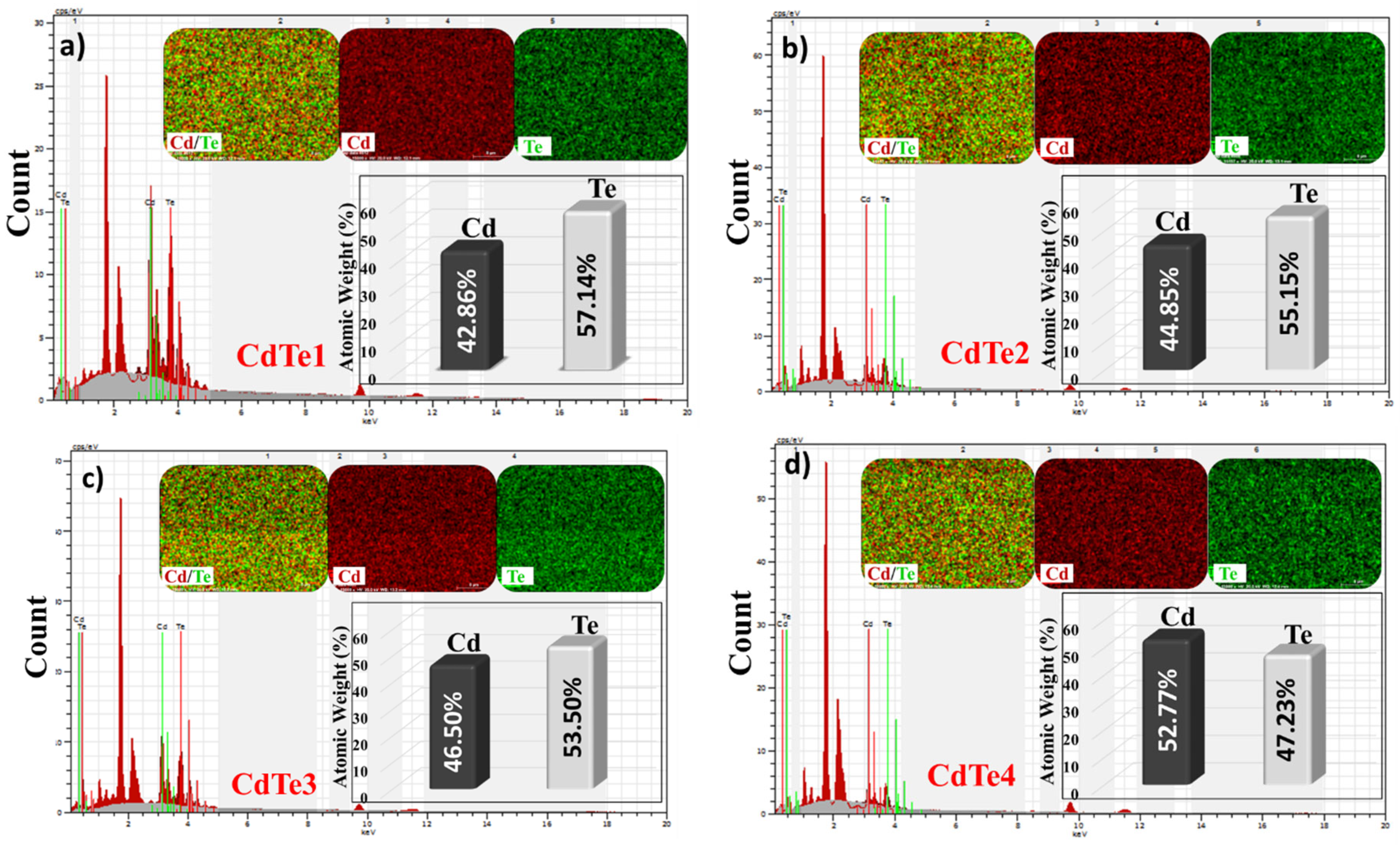
Figure 6.
Optical characterization of CdTe thin films: a) Absorbance spectra, b) Tauc plots for band-gap determination, and c) PL spectra.
Figure 6.
Optical characterization of CdTe thin films: a) Absorbance spectra, b) Tauc plots for band-gap determination, and c) PL spectra.
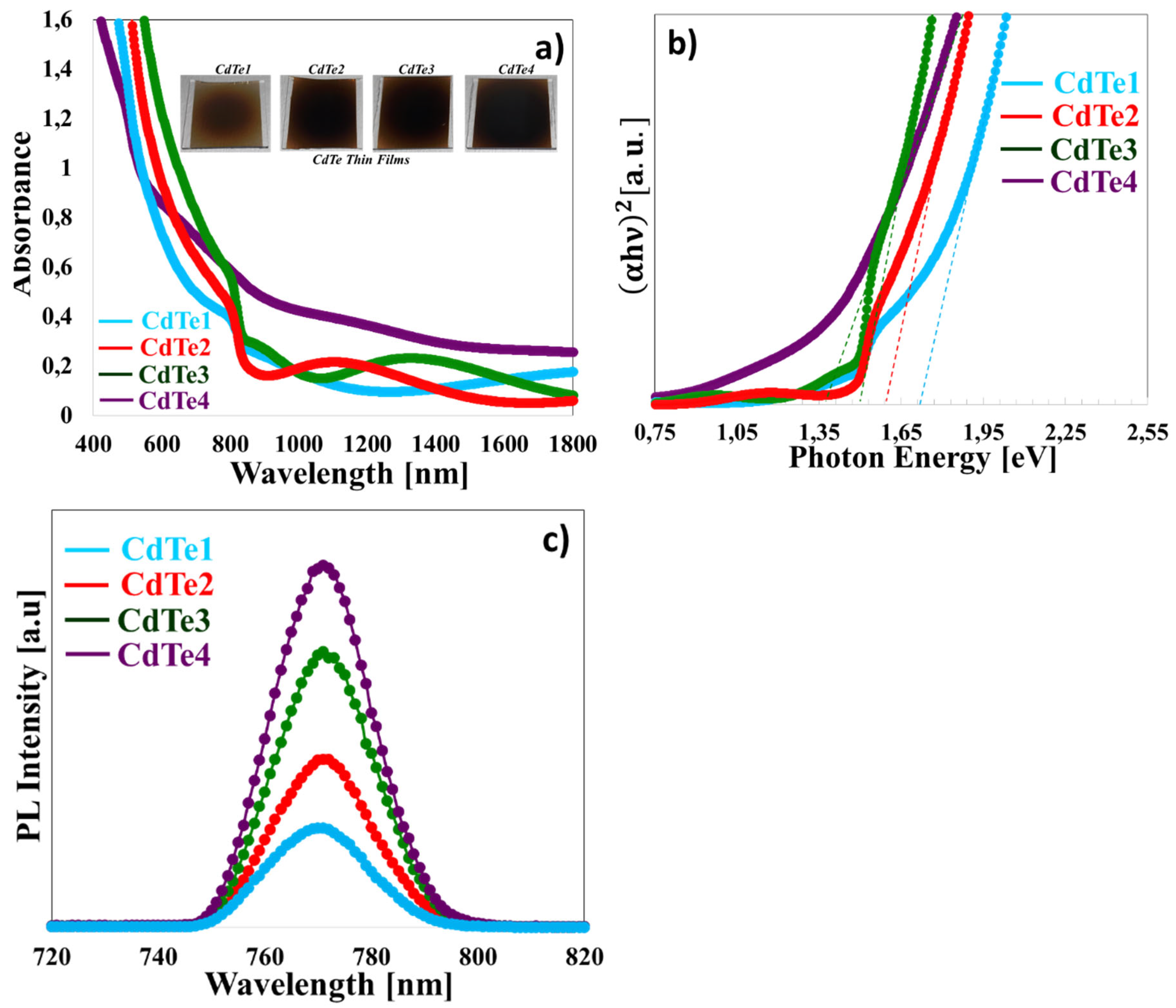
Figure 7.
a) Variation in the concentration ratio (C/C₀) of the MB dye solution under visible light irradiation in the presence of CdTe thin-film photocatalysts, b) pseudo-first-order kinetic plots for the photocatalytic degradation of MB under visible light irradiation, and c) temporal evolution of the UV-Vis absorption spectra of the MB solution during visible light photocatalysis using the CdTe3 thin film photocatalyst. d) Conceptual representation of the photocatalytic degradation of the MB dye solution driven by visible light using the CdTe3 thin-film photocatalyst.
Figure 7.
a) Variation in the concentration ratio (C/C₀) of the MB dye solution under visible light irradiation in the presence of CdTe thin-film photocatalysts, b) pseudo-first-order kinetic plots for the photocatalytic degradation of MB under visible light irradiation, and c) temporal evolution of the UV-Vis absorption spectra of the MB solution during visible light photocatalysis using the CdTe3 thin film photocatalyst. d) Conceptual representation of the photocatalytic degradation of the MB dye solution driven by visible light using the CdTe3 thin-film photocatalyst.
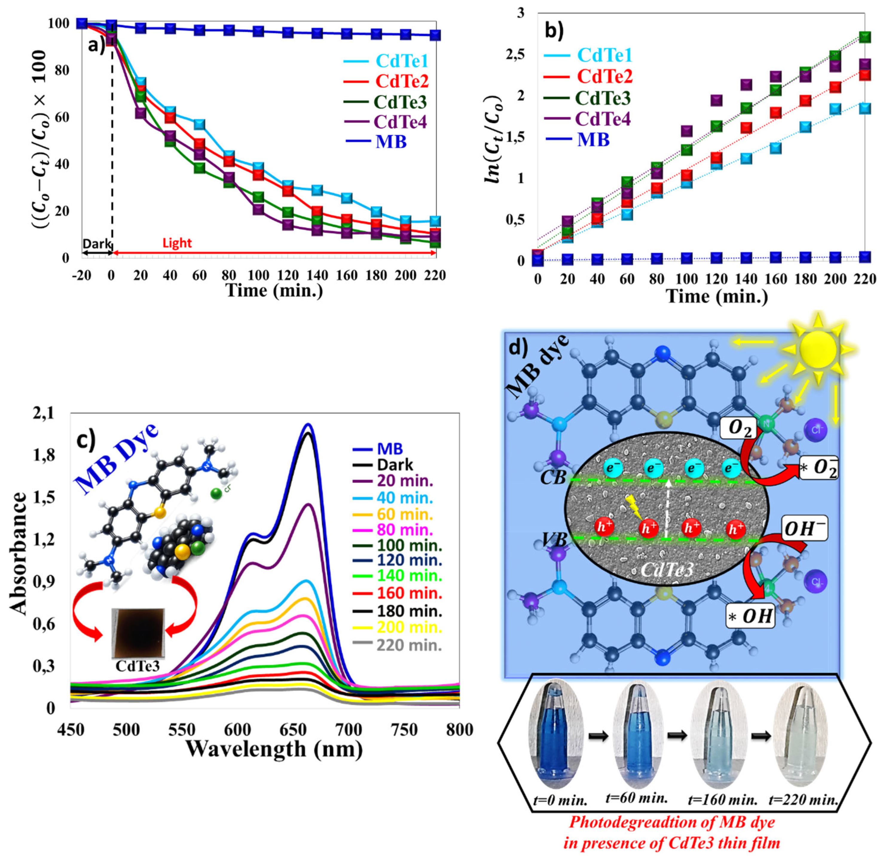
Figure 8.
a) Effect of solutions’ pH on the photodegradation concentration (C/C₀) of MB under visible light conditions with the CdTe thin films, and b) pseudo-first-order kinetic plots for the photocatalytic degradation of MB at different pH values under visible light c) Photocurrent response of CdTe thin films under visible-light irradiation using repeated light on/off cycles, and d) effect of radical scavengers (IPA, EDTA-2Na, and BQ) on the photocatalytic degradation of MB over the CdTe3 thin-film photocatalyst under visible-light irradiation.
Figure 8.
a) Effect of solutions’ pH on the photodegradation concentration (C/C₀) of MB under visible light conditions with the CdTe thin films, and b) pseudo-first-order kinetic plots for the photocatalytic degradation of MB at different pH values under visible light c) Photocurrent response of CdTe thin films under visible-light irradiation using repeated light on/off cycles, and d) effect of radical scavengers (IPA, EDTA-2Na, and BQ) on the photocatalytic degradation of MB over the CdTe3 thin-film photocatalyst under visible-light irradiation.
Disclaimer/Publisher’s Note: The statements, opinions and data contained in all publications are solely those of the individual author(s) and contributor(s) and not of MDPI and/or the editor(s). MDPI and/or the editor(s) disclaim responsibility for any injury to people or property resulting from any ideas, methods, instructions or products referred to in the content. |
© 2026 by the authors. Licensee MDPI, Basel, Switzerland. This article is an open access article distributed under the terms and conditions of the Creative Commons Attribution (CC BY) license (http://creativecommons.org/licenses/by/4.0/).
Copyright: This open access article is published under a Creative Commons CC BY 4.0 license, which permit the free download, distribution, and reuse, provided that the author and preprint are cited in any reuse.