Preprint
Article

This version is not peer-reviewed.

Structures Based on TiO2 and TiO2:Co Nanotubes: Electrical and Magnetic Behavior for Resistive Memories

Submitted:

24 August 2026

Posted:

26 August 2026

You are already at the latest version

Abstract

In this work, TiO2 and TiO2:Co nanotubes were fabricated via electrochemical anodization, using Ti (99.99% purity) and Ti/Co foils as the anode and cathode. Cobalt was deposited onto the Ti foils using the DC magnetron sputtering technique under a working pressure of 2.5×10⁻² Torr. The resulting nanotubes exhibited wall nodes and an average length of ~300 nm. The synthesized structures were characterized by X-ray diffraction (XRD), identifying anatase as the predominant phase, accompanied by an amorphous halo. Two types of MSM devices were fabricated to study bulk and surface conduction: a transverse configuration (TE/(TiO2, TiO2:Co)/Ti), with top electrodes (TE) Al or Au, and a coplanar configuration (Al/TiO2/Al). Topographic study was analyzed using Atomic Force Microscopy (AFM) and Kelvin Probe Force Microscopy (KPFM) in tapping mode. The device behavior is mainly governed by the TE/ TiO2 junction due to the absence of an energy barrier at the TiO2/Ti interface. All samples exhibit asymmetric I-V behavior with higher conduction under positive bias. The Au/ TiO2/Ti device showed the lowest resistance among Ti BE structures, displaying Schottky behavior with low reverse current leakage and a shift in the zero-current crossing depending on the scan direction. Barrier heights near the zero-current crossing, calculated via the thermionic emission model, were 0.91 eV and 0.70 eV for reverse and forward directions, respectively. Ideality factors and series resistance exceeded 6.8 and 40 kΩ, suggesting additional transport mechanisms. In addition, magnetization as a function of the applied field was realized to TiO2:Co nanotubes evidencing the ferromagnetic-like behavior.

Keywords: 
;  ;  ;  

1. Introduction

In 1996, DARPA introduced the term 'spintronics,' derived from SPIN TRansfer electrONICS, to spearhead the development of materials which use the degree of electron charge and spins of electrons [1]. Among spintronic materials, diluted magnetic semiconductors based on oxides (O-DMS) have emerged as a key component for integrating semiconducting and magnetic properties [2]. Notable properties of O-DMS include exhibiting ferromagnetic and antiferromagnetic behavior at room temperature [3], as well as the ability to control their resistive states (RS), making them promising candidates for non-volatile memory (NVM) applications [2].
TiO₂, a versatile wide-bandgap semiconductor, has emerged as a promising candidate in spintronic applications due to its exceptional structural and electronic properties. When doped with transition metal elements such as Co, Mn, or Fe, TiO₂ exhibits diluted magnetic semiconductor (DMS) behavior, enabling the integration of magnetic and semiconducting properties within a single material [3,4]. These dopants introduce localized magnetic moments and can mediate ferromagnetic or antiferromagnetic interactions, often observable at room temperature. Furthermore, the ability to tune its resistive switching (RS) properties through careful doping strategies positions TiO₂ as an ideal material for the development of multifunctional devices, such as magnetic-resistive random-access memories (MRAM). Therefore, TiO2 and doped TiO2, has emerged as a promising candidate in spintronic applications due to its exceptional structural and electronic properties [2,5].
However, understanding and controlling the interplay between its magnetic and resistive states remains a critical challenge, offering fertile ground for advancing spintronic technologies. The spintronic memristor, a magnetic memristor based on the spintronic effect of nanoelectrons, has emerged as a highly promising component in next-generation electronic and computational technologies [6,7]. By leveraging electron spin rather than solely relying on charge transport, this device overcomes several limitations of conventional memristors, particularly in terms of non-linearity arising from non-uniform doping and second-order effects [6,7,8]. It retains key advantages such as non-volatility, low power consumption, and ease of integration, while also exhibiting superior linearity, enhanced anti-interference performance, and improved reliability. These attributes make spintronic memristors highly attractive for applications in data storage, artificial intelligence, embedded systems [8], the Internet of Things (IoT) [9], and machine learning, where energy efficiency and stable performance are critical.
Furthermore, the continuously variable resistance of spintronic memristors, which is directly linked to charge variation over time, enables precise tunability and adaptability in real-time operational environments. As research continues to refine the material properties and device architectures, the development of spintronic memristors is expected to pave the way for more efficient, high-performance memory and computing technologies, reinforcing their role in the advancement of spintronic and quantum-based devices. Therefore, this work presents the fabrication and characterization of TiO2 and TiO2:Co nanotubes provide valuable insights into their structural, electronic, and transport properties, highlighting their potential for spintronic and resistive switching applications. The observed Schottky behavior, asymmetric I-V characteristics, and dependence on bias polarity suggest complex charge transport mechanisms, influenced by barrier heights and series resistance. These findings contribute to a deeper understanding of transition-metal-doped TiO2 nanostructures and their role in advanced electronic devices, paving the way for further studies on their integration into next-generation memory and spintronic systems.

2. Materials and Methods

The Materials and Methods should be described with sufficient details to allow others to replicate and build on the published results. Please note that the publication of your manuscript implicates that you must make all materials, data, computer code, and protocols associated with the publication available to readers. Please disclose at the submission stage any restrictions on the availability of materials or information. New methods and protocols should be described in detail while well-established methods can be briefly described and appropriately cited.
TiO2 and TiO2:Co nanotubes were fabricated via electrochemical anodization, using Ti foils (99.99% purity) with 50 µm and Ti/Co foils as the anode and Ti foils as cathode. Cobalt was deposited onto the Ti foils by the DC magnetron sputtering technique using a Cobalt target of 99.995% of purity, 50 W target power, under a working pressure of 2.5×10⁻² Torr and the deposition time was 30 min at room temperature. The electrochemical anodization process was carried out at room temperature in a solution containing 0.25 wt% ammonium fluoride (NH₄F), 2 wt% distilled water, and 97.75% ethylene glycol, the anodization process time was 12 min and the solution was maintaining to stirred a 250 rpm by 5 min. A square-wave voltage profile was applied (alternating voltage) characterized by 80 V for 1 min followed by 20 V during 5 minutes. The resulting nanotubes exhibited wall nodes and an average length of ~300 nm.
Al (99.99% of pure) and Au (99.99% of pure) top electrodes (TE) were vacuum-deposited onto the surface of the TiO2 and TiO2:Co via thermal evaporation. A tungsten boat was used at an evaporation temperature of 1473 K. Given the different mass and materials’ properties, the conditions for Al and Au evaporation were: 0.080g of Al wire held for 15s in a base pressure of 3.2 × 10⁻⁵ Torr, meanwhile 0.150g of Au pellets were held for 75s under a vacuum of 7.4 × 10⁻⁴ Torr.
Two types of devices were fabricated to evaluate bulk and surface conduction behavior. The first type was a transversal structure, where the bottom electrode (BE) consisted of the Ti film served as the substrate for the anodization process. The top electrode (TE) was either Au or Al, resulting in a TE/(TiO₂, TiO₂:Co)/Ti configuration. The second type was a coplanar structure with two aluminum electrodes (Al/TiO₂/Al). Electrical measurements were carried out using a Keithley 2460 SourceMeter picoammeter with Remote LAN 1588 Interlock, under ambient temperature and atmospheric pressure (see Figure 1). The voltage was scanned in the sequence: 0V→+3V→0→−3V→0V. Data analysis, including endurance measurements, was performed using computational tools.
The structural characterization of the synthesized samples was performed using X-ray diffraction (XRD) with a PANalytical X’Pert Pro diffractometer, equipped with a Cu-Kα radiation source (λ = 1.54 Å), operating at 40 kV and 40 mA, and an X’Celerator detector. The Rietveld refinement of the diffraction data was conducted using the X’Pert High Score Plus software. Morphological analysis was carried out using a Vega3 SB Scanning Electron Microscope (SEM) with a tungsten source, an XFlash Detector 410 M, and an acceleration voltage of 10 kV under high vacuum conditions (10⁻⁶ mbar). For SEM micrographs processing ImageJ software was used.
Magnetic measurements performed at room temperature using a superconducting quantum interference device (SQUID) (Quantum Design MPMS 3 SQUID in a Vibrating Sample Magnetometer (VSM) mode. The positive bias is defined as the current flowing from the BE to the TE. The films were evaluated by Atomic Force Microscopy (AFM) and Kelvin Probe Force Microscopy (KPFM) using a Cypher ES atomic force microscope (Asylum Research, USA) operating device/analyzer in tapping mode.

3. Results

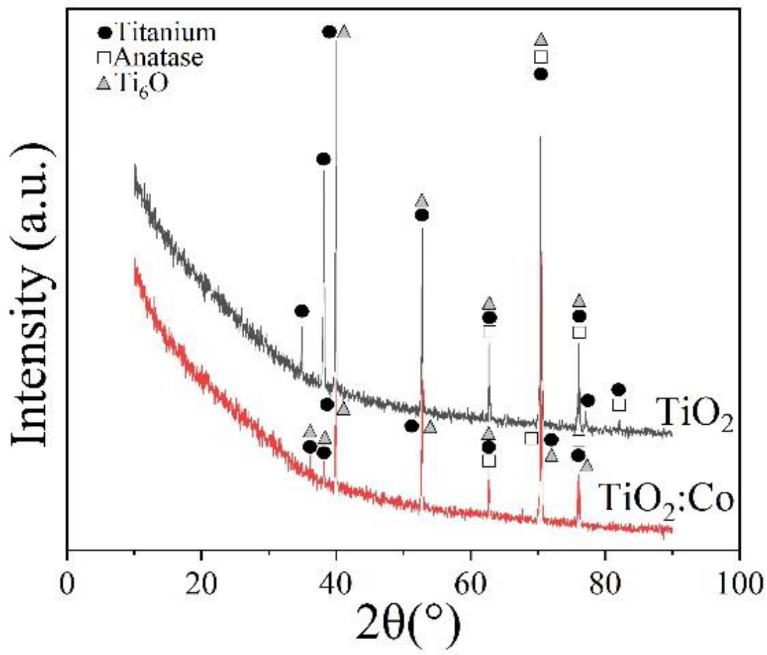
This section may be divided by subheadings. It should provide a concise and precise description of the experimental results, their interpretation, as well as the experimental conclusions that can be drawn. Figure 2 shows the XRD patterns for TiO2 and TiO2:Co nanotubes, synthesized with alternating voltage, at room temperature, without annealing process. It is evidenced the formation of anatase phase associated with the synthesis method and fabrication parameters, being the titanium the principal phase related to the substrate foil. Also, it is evidenced the presence of an amorphous halo without the formation of the Cobalt phases, it is linked the low concentration of Co (~0.04 ± 0.01 wt%) according to de EDXS measurements.
Under anodization conditions where oxygen availability is limited, or where the rate of oxide formation exceeds the rate of oxygen incorporation, substoichiometric phases of the Ti-O system can be generated. In particular, the Ti6O phase forms in locally reducing environments characterized by a high density of oxygen vacancies. This phase represents a titanium-rich structure, stabilized by the partial reduction of Ti4+ toward lower oxidation states (Ti3+ or Ti2+) importance of nanotube thickness in nonvolatile memory [10,11].
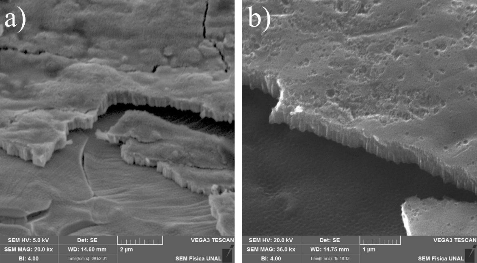
On the other hand, morphological characterization evidenced the formation of nanotubes with an average length of 92.63 ± 2.846 nm for TiO2:Co samples, whilst the TiO2 samples show a mean length of 308.6 ± 13.07 nm. These measurements were taken through SEM micrographs (see Figure 3) and with ImageJ software was realized the analysis of their sizes. Because the anodizing time is relatively short (12 min), close to the phase where the compact oxides are formed, and also due to the presence of Co that generates the formation of other complexes ([TiF6]2− and [CoF6]3− ) [2] within the electrolyte during anodizing, the attack is more difficult, which makes the difference in the size of the nanotubes in the samples.
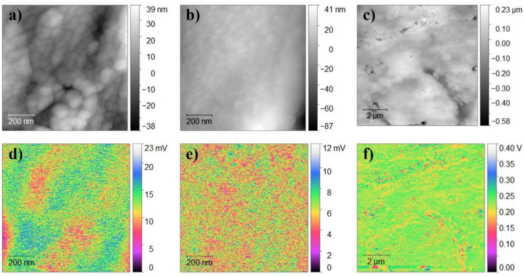
In addition, the analysis of the AFM micrographs reveals a textured surface characteristic of the nanotubular morphology of both TiO2 and TiO2:Co samples. However, the direct visualization of the inner diameters of the nanotubes is not feasible, as the AFM tip size is comparable to, or larger than, the inner diameters themselves. Consequently, the obtained topographic information primarily corresponds to the surrounding walls and external surface features of the nanotubes, rather than their hollow cores (see Figure 4a–c). This limitation must be considered when interpreting the surface morphology, as the AFM image reflects the convolution between the probe geometry and the sample topography. However, the KPFM maps present a slight correlation with the topography in areas deviated from the mean when the height range is about 0.8 μm (see Figure 4f). In a smaller height range (see Figure 4d,e), there is no evident correlation which indicates the absence of charge aggregates on the surface of the nanotubes in either TiO2 or TiO2:Co samples.
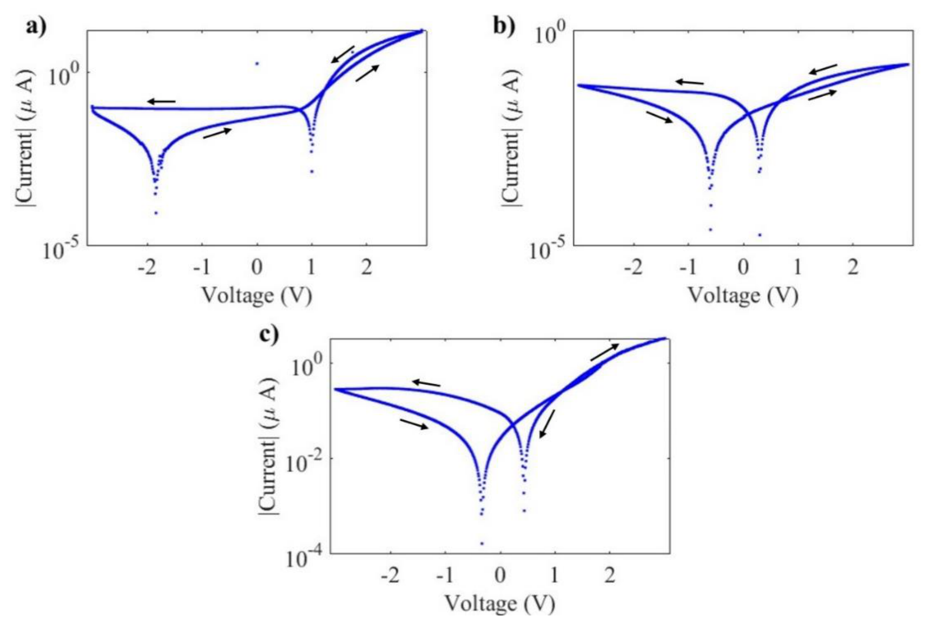
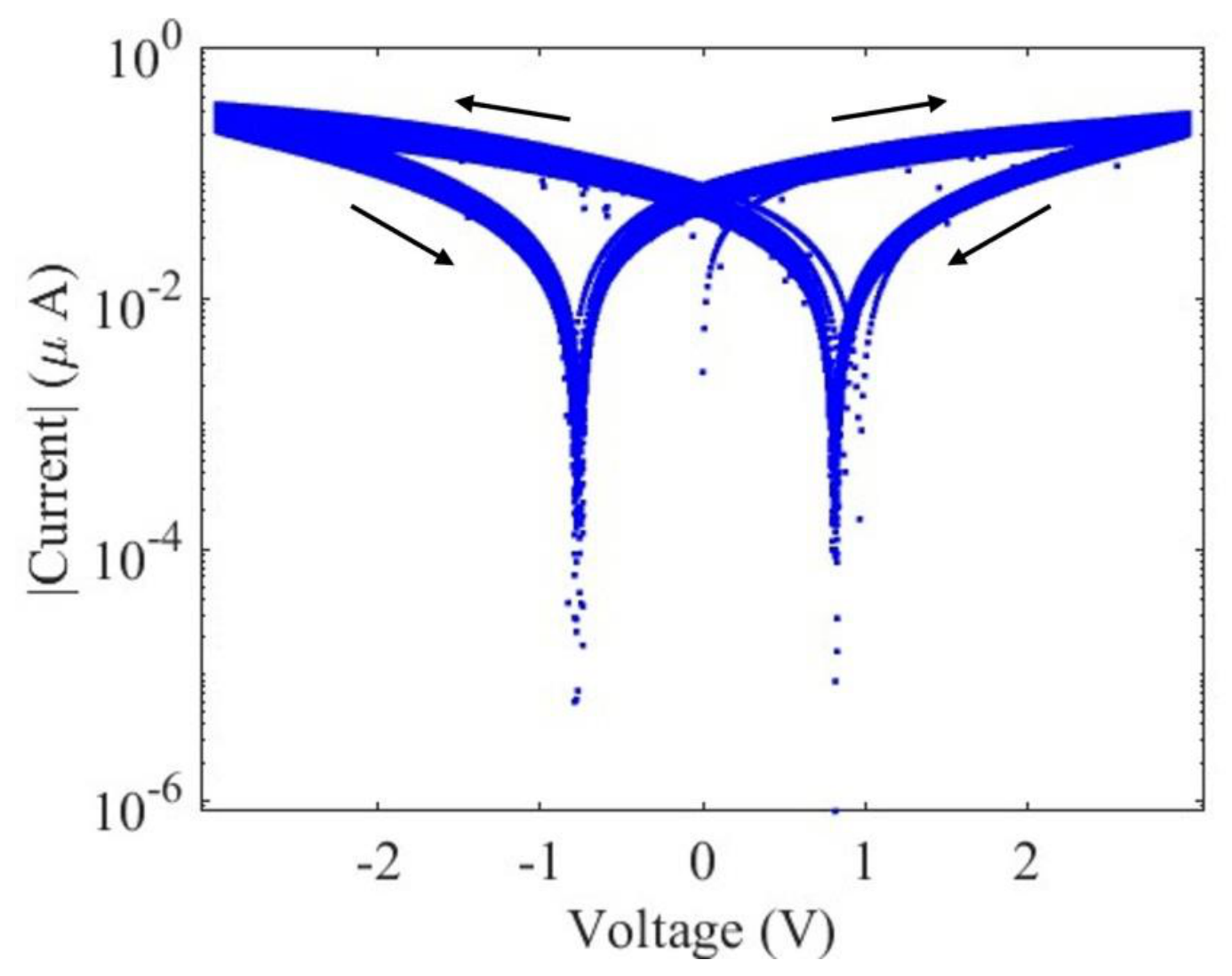
I-V characteristics of nanotubes obtained for the structures with Ti BE are shown in Figure 5 in semi logarithmic scale. The behavior is dominated by the TE and TiO2 junction given the zero-junction energy barrier in the TiO2/Ti interface [12]. All samples present asymmetrical I-V behavior with higher conduction at positive bias.
The Au/TiO2/Ti sample (see Figure 5a) has the least resistance among the Ti BE structures analyzed and it exhibits a Schottky behavior with low reverse current leakage and a shift of the zero current crossing in dependance on the scan direction, already seen in multiple Schottky junctions [13,14,15,16].
According to the thermionic emission, the electrical parameters obtained from the I-V curves and the method developed by Cheung and Cheung are presented in Table 1. The barrier heights were calculated near zero current, where the curves were still not deviated by other transport mechanisms such as trap assisted tunneling [15] and thermionic field emission [13], or local potential barriers [13], as indicated by the high ideality factors and large values of series resistances. Nevertheless, the calculated barrier heights are in good agreement with Au Work Function (5.1eV) and TiO2 electron affinity (4.33eV) reported in the literature [12,17], showing only small deviations attributable to the voltage scan direction.
Not Al TE devices can be explained merely with a Schottky barrier as there is a bipolar nonsymmetrical behavior (see Figure 5b, c), and a capacitive effect as a non-zero crossing point in the first quadrant [18]. Opposite to the increased conduction at positive bias, the hysteresis is stronger and more stable at negative bias. The asymmetry observed is consistent with the asymmetric layer stack.
The coplanar device (see Figure 6) exhibits purely capacitive behavior. This configuration lacks a Ti bottom electrode and instead includes two Al top electrodes. In contrast, the transversal devices with Al TE (see Figure 5b,c) display both capacitive and memristive characteristics, where the capacitive response originates from the Al/TiO₂ junction, while the memristive behavior is associated with the TiO₂/Ti interface. Additionally, the Al/TiO₂:Co junction exhibits a stronger capacitive response, as indicated by an increased crossing point compared to the TiO₂-based structure.
Compared to the Au junctions, the Al junctions exhibit a more complex behavior that cannot be explained solely by work function and electron affinity differences. The presence of interface states between Al and the nanotubes—possibly formed during the evaporation process—may account for the observed parasitic capacitance. Although the deposition was carried out under high-vacuum conditions, this may not have been sufficient to prevent Al from reacting with residual particles. Additionally, the annihilation or incomplete formation of conduction filaments, leading to the creation of a barrier region, has also been reported as a possible origin of capacitive effects in memristive devices [18].
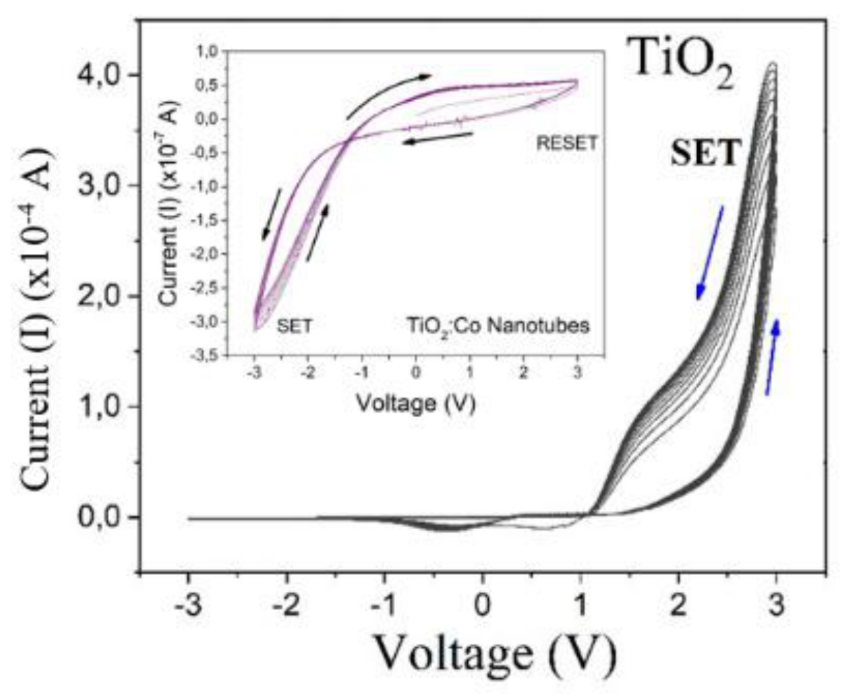
In the case of the transversal I-V measurements, TiO2 nanotubes presents a unipolar resistive switching behavior (see Figure 7). The SET state (High Resistance State (HRS)→Low Resistance State (LRS)) occurs in the positive region of the voltage, where there is an increase in current, and the RESET (LRS→ HRS) state at negative voltages. In the inset of the Figure 7, the I-V curves of the transversal section in the TiO2:Co nanotubes are presents. A bipolar resistive switching behavior can be observed evidenced by the RESET state occurs in the positive region of the voltage and the SET state occurs in the negative region of the voltage. During the SET state, the conductive filament is formed within the dielectric layer, whereas in the RESET state, this filament is either ruptured or redistributed, leading to a transition back to the high-resistance state [10].
The size of the nanotubes plays a critical role in memristive behavior. Thinner nanotube layers facilitate the formation of conductive filaments, enhancing the device’s switching performance. This filament formation underlies the resistive switching mechanism, enabling transitions between the high-resistance state (HRS) and the low-resistance state (LRS). The applied electric field and thermal effects induce the migration of free charge carriers—associated with amorphous TiO2 formation—and the generation of oxygen vacancies. When the density of these vacancies exceeds a critical threshold, they self-organize into a conductive filament. In TiO2-based resistive switching devices, the directionality and structural continuity of the nanotube walls further support and guide filament formation [2,19].
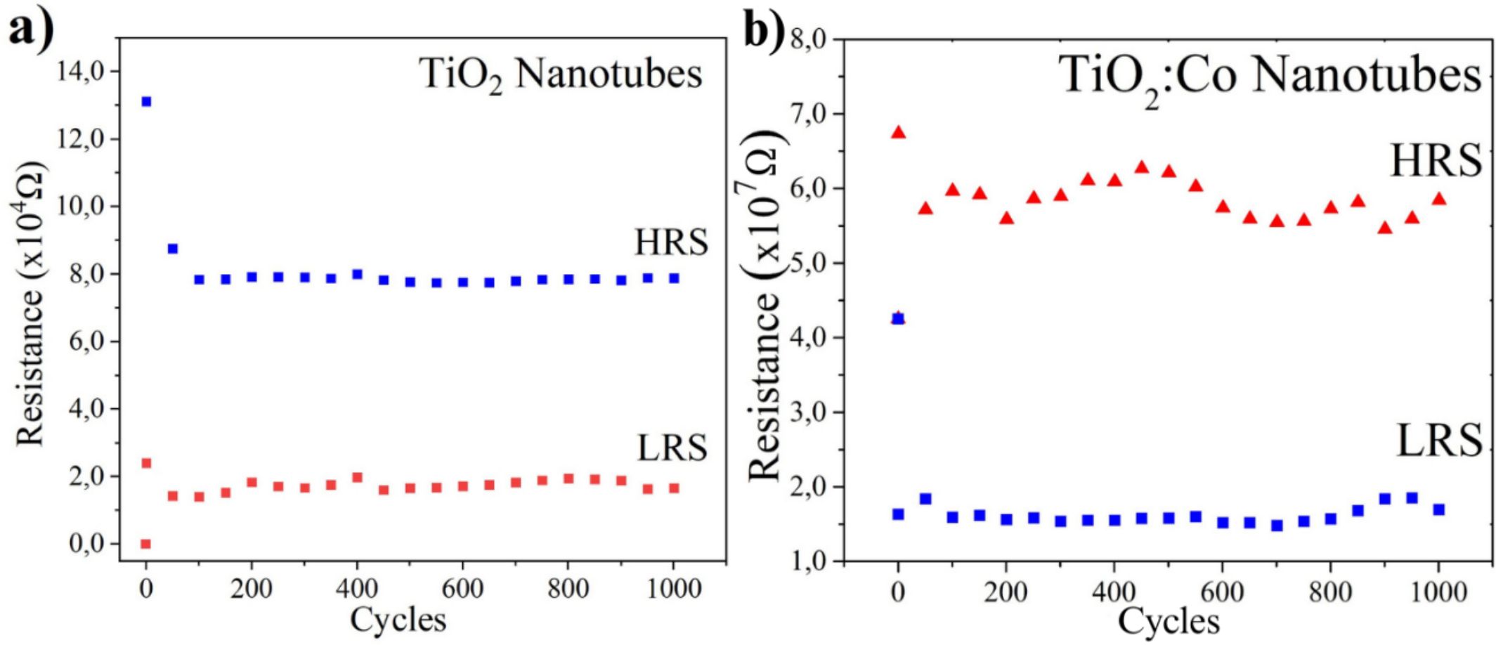
Otherwise, endurance performance measurements were also done to assess the repeatability of the high-resistance state (HRS) and low-resistance state (LRS) after 1000 sweep cycles (1200 data points per cycle), for both TiO2 and TiO2:Co nanotubes (see Figure 8). The repeatability of the resistive states (HRS and LRS) was established in the SET region, under a positive bias of 2.0 V for TiO2 nanotubes and in the RESET region under a positive bias of 0.5 V for TiO2:Co nanotubes.
As shown in Figure 8a for TiO₂ nanotubes, the first ~80 cycles exhibit the progressive formation of the conductive filament, followed by a stabilization of both the high-resistance state (HRS) and low-resistance state (LRS), likely due to the increased mobility of free electrons [2]. A similar trend is observed in the endurance test for TiO₂:Co nanotubes (Figure 8b), where the conductive filament formation also occurs during the initial cycles, after which the switching behavior stabilizes. In this case, the LRS values remain relatively stable, while the HRS shows minor fluctuations. The incorporation of Co into the TiO₂ matrix is believed to introduce defect states that enhance the operating voltage window and improve the endurance of the resistive switching process [2].
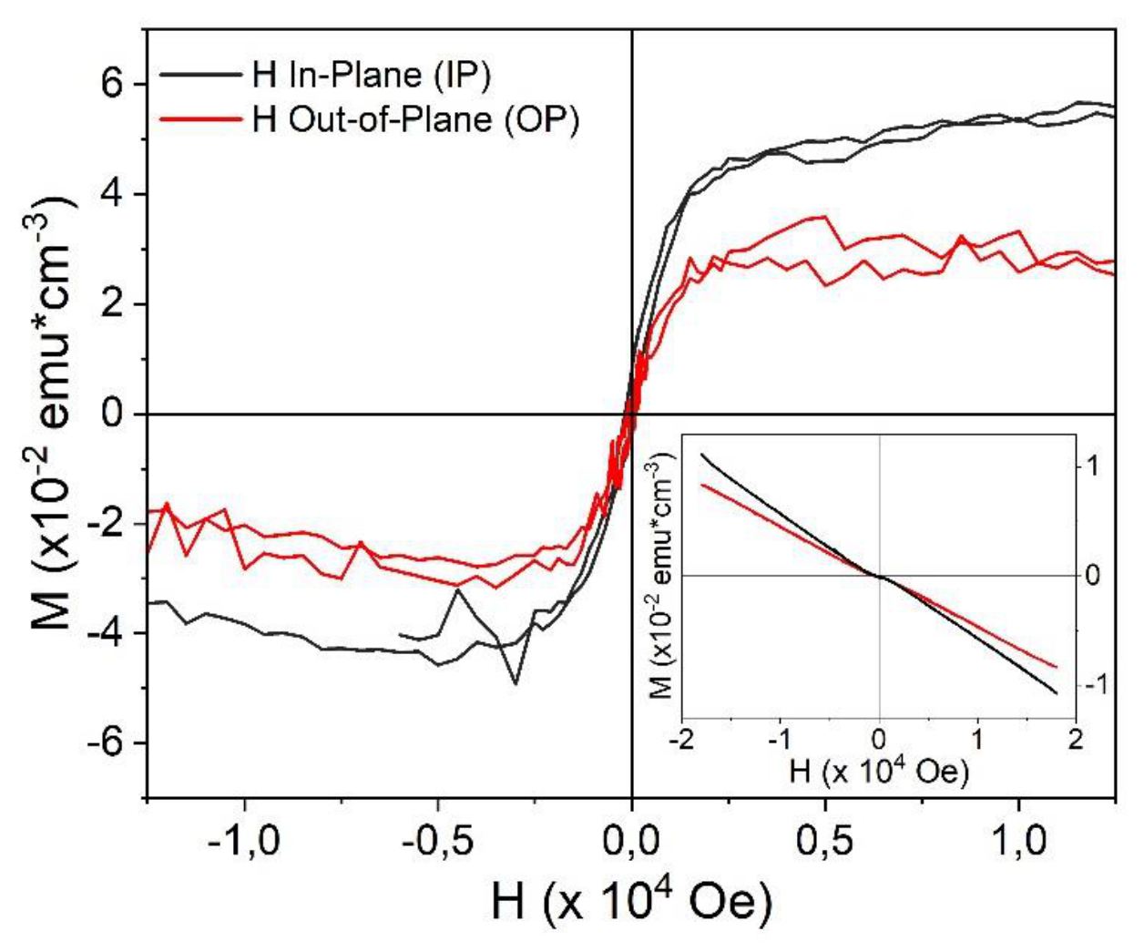
Other studies have demonstrated that these materials can obtain magnetic properties that can aid in the resistive processes of memristor-type memory by incorporating transition elements into the semiconductor oxide matrix [5,20,21]. According to reports, one mechanism that supports the existence of dipole moments and contributes to ferromagnetic-like behavior is the incorporation of Co atoms into the semiconductor matrix. In the Figure 9, it shows a magnetic behavior of the TiO2:Co nanotubes.
The magnetization (M) as a function of the applied magnetic field (H), measured with the field oriented in-plane (black line) and out-of-plane (red line), reveals the magnetic behavior of the TiO2:Co nanotubes. These measurements were corrected to remove the diamagnetic contributions from both the Ti substrate and the TiO2 matrix, thereby isolating the ferromagnetic-like response attributed to the system. This behavior is likely associated with weak exchange interactions between the magnetic moments of Co ions and the presence of structural defects within the TiO2 lattice [22,23]. The observed difference between the in-plane and out-of-plane magnetization curves suggests the presence of magnetocrystalline anisotropy [24], which may arise from the random spatial distribution of Co ions and their specific substitutional or interstitial positions within the semiconductor crystalline matrix. This observation is consistent with the Co concentration determined by EDXS analysis. The inset of Figure 9 shows the total magnetization, which includes the diamagnetic contribution from both the Ti foil substrate and the TiO2 semiconductor matrix.

4. Discussion

The structural, morphological, electrical, and magnetic results collectively demonstrate that the incorporation of Co into TiO₂ nanotubes significantly modifies the electronic transport mechanisms while preserving the anatase crystalline structure. XRD measurements revealed that anatase remains the dominant phase after Co incorporation, whereas no secondary cobalt-related crystalline phases were detected within the sensitivity limits of the technique. The absence of detectable Co clusters suggests that cobalt is either substitutionally incorporated into the TiO₂ lattice or distributed in highly dispersed defect-rich regions below the XRD detection threshold. Furthermore, the presence of an amorphous halo indicates a substantial degree of local structural disorder, which is expected to increase the density of defect states and oxygen-vacancy-related electronic levels. These defects play a crucial role in determining both the electrical conductivity and the magnetic response of oxide-based diluted magnetic semiconductors.
The SEM analysis revealed a pronounced reduction in nanotube length after cobalt incorporation, decreasing from approximately 309 nm in pure TiO₂ to about 93 nm in TiO₂:Co nanotubes. This behavior can be explained by the modification of the anodization kinetics induced by cobalt deposition prior to anodization. The formation of mixed fluoride complexes during electrochemical oxidation modifies the local dissolution and oxide growth rates, limiting nanotube elongation. Such morphological differences are expected to influence charge transport by modifying the effective conduction path and the density of structural defects distributed along the nanotube walls. Similar effects have been reported in transition-metal-doped TiO₂ systems, where dopants alter both nanotube growth dynamics and defect formation processes.
AFM and KPFM measurements provide additional insight into the surface electronic properties. Although the nanotubular morphology was clearly observed in the topographic images, no significant localized surface potential variations were detected. This observation suggests a relatively homogeneous distribution of charge across the nanotube surface and indicates that the dominant transport mechanisms are likely governed by bulk defect states and metal-semiconductor interfaces rather than by localized surface charge accumulation. The absence of large potential fluctuations is also consistent with the low cobalt concentration determined by EDXS measurements, which would not be expected to generate strong electronic phase segregation.
The electrical measurements indicate that charge transport is primarily controlled by the top metal/TiO₂ interface. The asymmetric current-voltage characteristics observed in both TiO₂ and TiO₂:Co devices are consistent with Schottky barrier formation at the top electrode, whereas the Ti/TiO₂ interface behaves closer to an ohmic contact due to the favorable alignment of the Ti work function with the TiO₂ conduction band. The lower resistance observed in Au/TiO₂/Ti structures compared with Al/TiO₂/Ti devices can be attributed to differences in work function and interface barrier formation. The extracted barrier heights near the zero-current crossing, together with the large ideality factors and series resistance values, indicate that pure thermionic emission cannot fully describe the transport behavior. Instead, conduction is likely assisted by defect-mediated mechanisms involving oxygen vacancies and localized electronic states distributed within the nanotube walls.
The magnetic measurements further support the role of defects in determining the physical properties of the system. The observed ferromagnetic-like response at room temperature in TiO₂:Co nanotubes is consistent with the behavior frequently reported in oxide-based diluted magnetic semiconductors [25]. Considering the low cobalt concentration and the absence of detectable cobalt-related crystalline phases, the magnetic response is likely associated with defect-assisted exchange interactions involving substitutional Co ions and oxygen-vacancy-related states. The coexistence of magnetic ordering and semiconducting transport makes TiO₂:Co nanotubes particularly attractive for multifunctional devices where electrical and magnetic properties can be simultaneously exploited.

5. Conclusions

TiO2 and TiO2:Co nanotubes were successfully synthesized through electrochemical anodization using pure Ti and Co-doped Ti foils. The proposed method led to the formation of amorphous structures as well as the anatase phase containing oxygen vacancies, which facilitate the incorporation of cobalt into the TiO2 lattice without the emergence of binary phases. This approach enabled the development of diluted magnetic semiconductors with nanotubular morphology. Furthermore, under anodization conditions with limited oxygen availability or where the oxide growth rate surpasses the oxygen incorporation rate, substoichiometric Ti–O phases such as Ti6O can be generated. Electrical response was evaluated showing the absence of charge aggregates in the surface. I-V curves were measured to evaluate bulk and surface conduction behavior. Bulk conduction exhibited two distinct behaviors depending on the top electrode material: Au TE formed a Schottky barrier as expected, while Al electrodes introduced an additional capacitive component, attributed to the Al/TiO₂ interface. Surface conduction was evaluated using two Al electrodes, where no memristive effect was observed—only purely capacitive behavior was detected. The resistive switching behavior exhibited by TiO2 and TiO2:Co nanotubes is associated with the formation of a conductive filament, generated by the migration of free charge carriers under an applied electric field. This mechanism enables the transition between a high-resistance state (HRS) and a well-defined low-resistance state (LRS). Endurance tests performed at room temperature demonstrated the reproducibility of the HRS and LRS, with stable switching observed at a positive bias of 2.0 V for TiO2 and 0.5 V for TiO2:Co nanotubes. Finally, the M vs H curves reveal that the magnetic response of the TiO2:Co nanotubes can be primarily governed by magnetocrystalline anisotropy, which originates from the structural and compositional characteristics of the Co-doped system and possibly related to defect-mediated ferromagnetism.

Author Contributions

For research articles with several authors, a short paragraph specifying their individual contributions must be provided. The following statements should be used Conceptualization, Jorge A. Calderón, Heiddy P. Quiroz, and A. Dussan; methodology, Jorge A. Calderón, Heiddy P. Quiroz, and A. Dussan.; software, Y. Porras Ramírez, D. Laverde Lizarazo, Jorge A. Calderón, Heiddy P. Quiroz, A. Dussan; validation, Jorge A. Calderón, Heiddy P. Quiroz, and A. Dussan.; formal analysis, Y. Porras Ramírez, D. Laverde Lizarazo, Jorge A. Calderón, Heiddy P. Quiroz, A. Dussan; investigation, Y. Porras Ramírez, D. Laverde Lizarazo, Jorge A. Calderón, Heiddy P. Quiroz, A. Dussan; resources, Y. Porras Ramírez, D. Laverde Lizarazo, Jorge A. Calderón, Heiddy P. Quiroz, A. Dussan; data curation, Y. Porras Ramírez, D. Laverde Lizarazo, Jorge A. Calderón, Heiddy P. Quiroz, A. Dussan; writing—original draft preparation, Y. Porras Ramírez, D. Laverde Lizarazo, Jorge A. Calderón, Heiddy P. Quiroz, A. Dussan; writing—review and editing, Jorge A. Calderón, Heiddy P. Quiroz, and A. Dussan; visualization, Y. Porras Ramírez, D. Laverde Lizarazo, Jorge A. Calderón, Heiddy P. Quiroz, A. Dussan; supervision, Jorge A. Calderón, Heiddy P. Quiroz, and A. Dussan; project administration, Jorge A. Calderón, Heiddy P. Quiroz, and A. Dussan; funding acquisition, Jorge A. Calderón, Heiddy P. Quiroz, and A. Dussan. All authors have read and agreed to the published version of the manuscript.

Funding

This research was funded by Universidad Nacional de Colombia through QUIPU 202010042199, and MinCiencias through Conv. 937.

Data Availability Statement

Data sets generated during the current study are available from the corresponding author on reasonable request.

Acknowledgments

The Universidad Nacional de Colombia supported this work via project QUIPU 202010042199, MinCiencias through Conv. 937. Special acknowledgment to Cluster in Convergent Sciences and Technologies of the Universidad Central for your support in this research.

Conflicts of Interest

The authors declare no conflicts of interest.

Abbreviations

The following abbreviations are used in this manuscript:
KPFM Kelvin Probe Force Microscopy
SEM Scanning Electron Microscopy
XRD X-Ray Diffraction
TE Top Electrode

References

  1. Bhardwaj, Pankaj; Singh, Jarnail; Verma, Vikram; Kumar, Ravi. Harnessing the duality of magnetism and conductivity: A review of oxide based dilute magnetic semiconductors. Phys. B Condens. Matter. 2025, 696, 416596. [Google Scholar] [CrossRef]
  2. Jaimes, Kimy S.; Quiroz, Heiddy P.; Calderón, Jorge A.; Dussan, A. Magnetic-resistive random access memories based on diluted Co-TiO2 nanotubes. Results Phys. 2024, 63, 107890. [Google Scholar] [CrossRef]
  3. Lee, Jaejun; Song, Kibum; Shin, Keun-Young; Lee, Woongkyu. Improved resistive switching characteristics of Au/TiO2/Au memristors on PDMS substrates with pyramid arrays. Mater. Sci. Eng. B. 2025, 314, 117986. [Google Scholar] [CrossRef]
  4. Chen. A review of emerging non-volatile memory (NVM) technologies and applications. Solid-State Electron. 2016, 125, 25–38. [Google Scholar] [CrossRef]
  5. Quiroz, Heiddy P.; Calderón, Jorge A.; Dussan, A. Magnetic switching control in Co/TiO2 bilayer and TiO2:Co thin films for Magnetic-Resistive Random Access Memories (M-RRAM). J. Alloy Compd. 2020, 840, 155674. [Google Scholar] [CrossRef]
  6. Wen, Changbao; Zhang, Xiaoxia; Guo, Xiaoding; Ru, Feng; Quan, Si. Flame intensity sensor based on the resistive and memory properties of spintronic memristor. Sens. Actuators A Phys. 2024, 377, 115722. [Google Scholar] [CrossRef]
  7. Wen, Changbao; Xu, Li; Zha, Jun; Zhou, Chenglong. A novel nuclear radiation cumulant sensor based on spintronic memristor. Sens. Actuators A Phys. 2022, 346, 113842. [Google Scholar] [CrossRef]
  8. Paulo, G.; Sun, K.; Di Muccio, G.; Gubbiotti, A.; Morozzo della Rocca, B.; Geng, J.; Maglia, G.; Chinappi, M.; Giacomello, A. Hydrophobically gated memristive nanopores for neuromorphic applications. Nat. Commun. 2023, 14, 8390. [Google Scholar] [CrossRef]
  9. Lin, Y.; Zhang, Q.; Gao, B.; Tang, J.; Yao, P.; Li, C.; Huang, S.; Liu, Z.; Zhou, Y.; Liu, Y.; Zhang, W.; Zhu, J.; Qian, H.; Wu, H. Uncertainty quantification via a memristor Bayesian deep neural network for risk-sensitive reinforcement learning. Nat. Mach. Intell. 2023, 5, 714–723. [Google Scholar] [CrossRef]
  10. Kornilov, I.I.; Vavilova, V.V.; Fykin, L.E.; Ozerov, R.P.; Solov'ev, S.P.; Smirnov, V.P. Neutron diffraction Investigation of Ordered Structures in the Titanium-Oxigen System. Metall. Trans. 1970, 1, 2569. [Google Scholar] [CrossRef]
  11. Bell, Crystal N.; Lee, Dong-Chan; Drexler, Matthew N.; Rouleau, Christopher M.; Sasaki, Kotaro; Senanayake, Sanjaya D.; Williams, Michael D.; Alamgir, Faisal M. Substoichiometric Tuning of the Electronic Properties of Titania. Thin Solid Films 2021, 717, 138437. [Google Scholar] [CrossRef]
  12. Hossein-Babaei, F.; Lajvardi, M. M.; Alaei-Sheini, N. The energy barrier at noble metal/TiO2 junctions. Appl. Phys. 2015, 106, 083503. [Google Scholar] [CrossRef]
  13. Splith, D.; Müller, S.; von Wenckstern, H.; Grundmann, M. Numerical Modeling of Schottky Barrier Diode Characteristics. Phys. Status Solidi A 2021, 218, 2100121. [Google Scholar] [CrossRef]
  14. Yu, S.; Zhang, C.; Yang, P.; et al. Effect of annealing temperature on structural and electrical properties of Al/Nb-doped TiO2 Schottky diodes on Pt–Si substrates. J. Mater. Sci. Mater. Electron. 2019, 30, 18287–18295. [Google Scholar] [CrossRef]
  15. Zhang, Y.; Mauze, A.; Alema, F.; Osinsky, A.; Speck, J. S. Near unity ideality factor for sidewall Schottky contacts on un-intentionally doped β-Ga2O3. Appl. Phys. Express 2019, 12, 044005. [Google Scholar] [CrossRef]
  16. Zhao, G.; Yin, Y.; Peng, Y.; et al. Effect of hydrogen ions in the adsorbed water layer on the resistive switching properties of hexagonal WO3 nanowire. J. Appl. Phys. 2019, 126, 054303. [Google Scholar] [CrossRef]
  17. Endo, Raimu; Siriwardena, Hirulak D.; Kondo, Atsuyoshi; Yamamoto, Chisato; Shimomura, Masaru. Structural and chemical analysis of TiO2 nanotube surface for dye-sensitized solar cells. Appl. Surf. Sci. 2018, 439, 954–962. [Google Scholar] [CrossRef]
  18. Qingjiang, L.; Khiat, A.; Salaoru, I.; et al. Memory Impedance in TiO2 based Metal-Insulator-Metal Devices. Sci. Rep. 2014, 4, 4522. [Google Scholar] [CrossRef]
  19. Quiroz, Heiddy P.; Serrano, J.E.; A. Dussan, A. Magnetic behavior and conductive wall switching in TiO2 and TiO2:Co self-organized nanotube arrays. J. Alloys Compd. 2020, 825, 154006. [Google Scholar] [CrossRef]
  20. Terán, Cristian L.; Calderón, Jorge A.; Quiroz, Heiddy P.; Dussan, A. Optical properties and bipolar resistive switching of ZnO thin films deposited via DC magnetron sputtering. Chin. J. Phys. 2021, 74, 1–8. [Google Scholar] [CrossRef]
  21. Quiroz, Heiddy P.; Galíndez, E. F.; Dussan, A.; Cardona-Rodriguez, A.; Ramirez, Juan Gabriel. Super-exchange interaction model in DMOs: Co doped TiO2 thin films. J. Mater. Sci. 2021, 56, 581–591. [Google Scholar] [CrossRef]
  22. Stiller, M. Defect Induced Magnetism in Titanium Dioxide. Doctoral thesis, University of Leipzig, Faculty of Physics and Earth Sciences, 2020. [Google Scholar]
  23. Kumar, Shalendra; Kumari, Kavita; Kumar, Akshay; Koo, B.H.; Kumar, Rajesh; Alvi, P.A.; Dalela, Saurabh. 24 - Magnetism of titanium dioxide. In Defect-Induced Magnetism in Oxide Semiconductors, United Kingdom; 2023; pp. 563–584. [Google Scholar]
  24. Hosseinpour, P.M.; Jiménez-Villacorta, F.; Liu, J.; Assaf, B.A.; McDonald, I.J.; Arena, D.; Heiman, D.; Menon, L.; Lewis, L.H. Fe-incorporated TiO2 nanotube arrays: Electronic structure and magnetic response. Phys. Rev. B 2018, 98, 195145. [Google Scholar] [CrossRef]
  25. Dussan, Heiddy P.; Quiroz; Calderón, Jorge A. Nanomateriales que revolucionan la tecnología: perspectivas y aplicaciones en espintrónica; Editorial UN, Colombia, 2020; pp. 53–77. [Google Scholar]
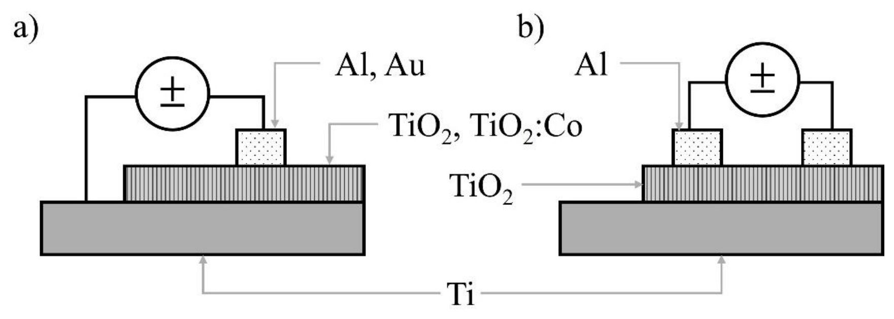
Figure 1. Schematic mechanism of a) transversal and b) coplanar structure of I-V measurements.
Preprints 229987 g001
Figure 2. XRD patterns for TiO2 nanotubes (black line) an TiO2:Co nanotubes (red line).
Preprints 229987 g002
Figure 3. SEM micrographs of a) TiO2 nanotubes and b) TiO2:Co nanotubes.
Preprints 229987 g003
Figure 4. Topography (top row, a–c) and Kelvin probe force microscopy (KPFM) surface potential maps (bottom row, d–f) for TiO₂-based samples. Images were acquired over scan areas of 1 μm² for TiO₂ (a, d), 1 μm² for TiO₂:Co (b, e), and 100 μm² for TiO₂ (c, f). KPFM maps are leveled to zero for comparison.
Preprints 229987 g004
Figure 5. I-V curves of the samples with transversal structures: a) Au/TiO2/Ti, b) Al/TiO2/Ti, and Al/TiO2:Co/Ti.
Preprints 229987 g005
Figure 6. I-V curve for 50 cycles of the coplanar structure Al/TiO2/Al.
Preprints 229987 g006
Figure 7. I-V curve for 10 cycles of the TiO2 nanotubes. Inset show I-V curve of TiO2:Co nanotubes.
Preprints 229987 g007
Figure 8. Endurance performance measurements for a) TiO2 nanotubes, and b) TiO2:Co nanotubes.
Preprints 229987 g008
Figure 9. Magnetization (M) as a function of external magnetic field (H) curves. Red line represents the measure obtained applying H parallel to sample surface, whilst, black line corresponds to the measure obtained when H is perpendicular to the sample surface.
Preprints 229987 g009
Table 1. Schottky barrier parameters in the transversal structure Au/TiO2/Ti.
Reverse direction Forward direction
Parameters ln I - V dV/dln(I) - V ln I - V dV/dln(I) – V
n 8.72 6.8 16.68 12.11
φ 0.91 eV - 0.70 eV -
Rs - 70 kΩ - 40 kΩ
Disclaimer/Publisher’s Note: The statements, opinions and data contained in all publications are solely those of the individual author(s) and contributor(s) and not of MDPI and/or the editor(s). MDPI and/or the editor(s) disclaim responsibility for any injury to people or property resulting from any ideas, methods, instructions or products referred to in the content.
Copyright: This open access article is published under a Creative Commons CC BY 4.0 license, which permit the free download, distribution, and reuse, provided that the author and preprint are cited in any reuse.